Note: Descriptions are shown in the official language in which they were submitted.
1
LIGHT SHAPING ASSEMBLY HAVING LIGHT SOURCES MOUNTED ON A PCB
VIA SUPPORTING PINS BENT FOR ORIENTING LIGHT TOWARD A PROJECTOR
LENS
FIELD
[01] The present technology relates to lighting control technologies. In
particular, various light
shaping assemblies having light sources mounted on a printed circuit board via
supporting pins
that are bent for orienting light toward a projector lens are disclosed.
BACKGROUND
[02] An innovative device projecting a two-dimensional (2D) pixel matrix, in
which each
"pixel" of the 2D matrix consists of an infrared (IR) digital data stream, is
described in US Patent
No. 8,628,198. Since the 2D pixel matrix is projected upon, for example,
members of an audience
in a stadium, it is possible to transmit different data to different locations
in the stadium, so the
data received in a particular location can be made specific to a pixel
projected to that location.
Since each IR digital data stream may be location dependent, various IR
digital data streams can
be programmed to be unique in content, so that each pixel may be given, if
desired, unique
instructions, particular to that pixel or stadium location. Receivers of this
IR digital data stream,
being worn by members of the audience, are thus provided with unique
instructions, commands,
or data, which may be made dependent upon which pixel, or physical location,
they occupy. A
movement of a receiver from one pixel location to another automatically
changes that receiver's
data stream to that transmitted to the new location. The IR digital data
stream, if programmed to
illuminate the receiver according to color and intensity information, can turn
the receivers into a
real time, moving light show. The technology described in US Patent No.
8,628,198 is thus capable
of transforming the audience into a 2D video screen.
[03] Even though the recent developments identified above may provide
benefits,
improvements are still desirable. In particular, empty spaces, or voids, may
be present between the
various pixels projected on the audience, potentially leaving some of the
members of the audience
unable to receive the IR digital data stream. Manufacturing costs of the
technology may also be a
Date Recue/Date Received 2021-09-09
2
cause for concern. Also, the potential of the technology may not have been
fully exploited for other
applications.
[04] The subject matter discussed in the background section should not be
assumed to be prior
art merely as a result of its mention in the background section. Similarly, a
problem mentioned in
the background section or associated with the subject matter of the background
section should not
be assumed to have been previously recognized in the prior art. The subject
matter in the
background section merely represents different approaches.
SUMMARY
[05] Embodiments of the present technology have been developed based on
developers'
appreciation of shortcomings associated with the prior art.
[06] In particular, such shortcomings may comprise the presence of voids
between the various
pixels, manufacturing costs related to the prior technology, and/or lack of
use of the full potential
of the prior technology.
[07] In a first aspect, various implementations of the present technology
provide a combination,
comprising:
at least one lens; and
at least one prism;
the at least one lens and the at least one prism being in an optical path of a
corresponding at least one light source, the combination being configured to
direct light
radiating from the at least one light source toward a projector lens.
[08] In some implementations of the present technology, the at least one light
source comprises
an array of light sources; and the combination is configured to direct light
radiating from the array
of light sources toward the projector lens.
[09] In some implementations of the present technology, the at least one lens
is a Fresnel lens
and the at least one prism is a Fresnel prism.
Date Recue/Date Received 2021-09-09
3
[10] In some implementations of the present technology, the at least one lens
has a positive
focus.
[11] In some implementations of the present technology, the combination shapes
the light
radiating from the at least one light source as a cone-shaped light radiation
pattern directed toward
the projector lens.
[12] In some implementations of the present technology, the combination is
positioned at a
given distance from the at least one light source; and a focussing distance of
the at least one lens
is determined at least in part according to the given distance.
[13] In some implementations of the present technology, an orientation of the
at least one prism
is determined at least in part to correct a bending angle of the light
radiating from the at least one
light source.
[14] In some implementations of the present technology, the at least one lens
and the at least
one prism are formed as a single piece.
[15] In some implementations of the present technology, the projector lens is
selected from a
fixed lens, a parfocal lens and a varifocal lens.
[16] In some implementations of the present technology, the light radiating
from the at least one
light source forms an image pixel.
[17] In some implementations of the present technology, the image pixel
contains infrared light
carrying a digital data stream.
[18] In some implementations of the present technology, the at least one lens
comprises a
plurality of lenses; the at least one prism comprises a plurality of prisms;
and the combination
comprises a plurality of pixel forming sub-combinations, each pixel forming
sub-combination
comprising one of the plurality of lenses and a corresponding one of the
plurality of prisms, each
pixel forming sub-combination being configured to direct light radiating from
a corresponding set
of one or more light sources toward the projector lens.
Date Recue/Date Received 2021-09-09
4
[19] In some implementations of the present technology, at least some of the
plurality of pixel
forming sub-combinations are formed into a single optical sheet.
[20] In some implementations of the present technology, the single optical
sheet is a plastic
sheet.
[21] In some implementations of the present technology, the plurality of
lenses and the plurality
of prisms are on a same side of the single optical sheet.
[22] In some implementations of the present technology, the plurality of
lenses is on a first side
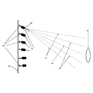
of the single optical sheet and the plurality of prisms on is a second side of
the single optical sheet,
the second side being opposite from the first side.
[23] In some implementations of the present technology, each of the plurality
of pixel forming
sub-combinations has specific optical properties determined at least in part
according to a specific
distance and a specific angle between the corresponding set of one or more
light sources and the
projector lens.
[24] In some implementations of the present technology, a focussing distance
of a given pixel
forming sub-combination is determined at least in part according to a distance
between the given
pixel forming sub-combination and the corresponding set of one or more light
sources.
[25] In some implementations of the present technology, the sets of one or
more light sources
corresponding to the plurality of pixel forming sub-combinations are
distributed over a first two-
dimensional area on a mounting support; the plurality of pixel forming sub-
combinations is
distributed over a second two-dimensional area of the combination; and the
specific optical
properties of a given pixel forming sub-combination are determined at least in
part according to a
distance, an angle and an angle of rotation between the given pixel forming
sub-combination and
the corresponding set of one or more light sources.
[26] In some implementations of the present technology, a first angle of
deflection of a first
pixel forming sub-combination located on an external edge of the second-two
dimensional area is
greater than a second angle of deflection of a second pixel forming sub-
combination located closer
to a center of the second two-dimensional area of the combination.
Date Recue/Date Received 2021-09-09
5
[27] In some implementations of the present technology, the plurality of sub-
combinations is
distributed over a two-dimensional (2D) array.
[28] In some implementations of the present technology, the 2D array forms a
rectangular
matrix.
[29] In some implementations of the present technology, the light radiating
from each
corresponding set of one or more light sources forms an image pixel.
[30] In some implementations of the present technology, each image pixel
contains infrared
light carrying a corresponding digital data stream.
[31] In a second aspect, various implementations of the present technology
provide a device,
comprising:
an enclosure having:
a rear opening adapted to receive a light beam from a light source,
a front opening adapted to emit a modified light beam, and
internal walls extending between the rear opening and the front opening;
the light beam being modified according to a perimeter of the front opening.
[32] In some implementations of the present technology, the perimeter of the
front opening
forms a rectangle.
[33] In some implementations of the present technology, an internal perimeter
of the enclosure
is rectangular.
[34] In some implementations of the present technology, the front opening of
the enclosure is a
plane of focus for the device.
[35] In some implementations of the present technology, the device further
comprises a
reflective material covering the internal walls of the enclosure.
Date Recue/Date Received 2021-09-09
6
[36] In some implementations of the present technology, the internal walls of
the enclosure are
made of a reflective material.
[37] In some implementations of the present technology, the enclosure further
comprises a rear
reflector plate, the rear opening being formed as a cut-out in the rear
reflector plate, a face of the
rear reflector plate on the inside of the enclosure being covered with a
reflective material.
[38] In some implementations of the present technology, the enclosure further
comprises a rear
reflector plate, the rear opening being formed as a cut-out in the rear
reflector plate, the rear
reflector plate being made of a reflective material.
[39] In some implementations of the present technology, a size of the cut-out
in the rear reflector
plate is selected to allow most of the light beam from the light source to
enter the enclosure.
[40] In some implementations of the present technology, the reflective
material is a textured
reflective material.
[41] In some implementations of the present technology, the rear opening is
centrally positioned
in an internal perimeter of the enclosure.
[42] In some implementations of the present technology, the device further
comprises a Fresnel
lens positioned in front of the enclosure so to receive the modified light
beam from the front
opening of the enclosure, a plane of focus of the device being located in
front of the Fresnel lens.
[43] In some implementations of the present technology, the device is adapted
to be positioned
at a distance from the light source so to leave an air gap between the light
source and the device.
[44] In some implementations of the present technology, the device further
comprises at least
one shade formed of a light absorbing material, the at least one shade being
adapted to attenuate
light emitted from the device outside of a main direction of the modified
light beam.
[45] In some implementations of the present technology, the light beam from
the light source is
an infrared light beam carrying a digital data stream; and the device is
configured to maintain
integrity of the digital data stream in the modified light beam.
Date Recue/Date Received 2021-09-09
7
[46] In a third aspect, various implementations of the present technology
provide a combination,
comprising:
the above described device and the light source;
a printed circuit board for mounting the light source; and
a reflective material covering a surface of the printed circuit board
surrounding the
light source.
[47] In a fourth aspect, various implementations of the present technology
provide a light
shaping assembly, comprising a two-dimensional (2D) array formed of a
plurality of devices as
defined above, each one of the plurality of devices being adapted to receive a
light beam from a
corresponding light source.
[48] In some implementations of the present technology, each device of the 2D
array is adapted
to emit a corresponding light pixel.
[49] In some implementations of the present technology, each light pixel
carries a respective
digital data stream.
[50] In some implementations of the present technology, the light shaping
assembly further
comprises a light absorbing hood positioned in front of the plurality of
devices and surrounding a
2D array formed by the modified light beams emitted by the plurality of
devices, the light
absorbing hood being adapted to attenuate light emitted from the light shaping
assembly outside
of a main direction of the modified light beams.
[51] In some implementations of the present technology, the 2D array forms a
rectangular
matrix.
[52] In some implementations of the present technology, the light shaping
assembly further
comprises a Fresnel lens positioned in front of the front openings of the
devices of the 2D array.
[53] In a fifth aspect, various implementations of the present technology
provide a method for
transmitting control instructions to a plurality of receivers, the method
comprising:
Date Recue/Date Received 2021-09-09
8
modulating a plurality of light sources to generate a plurality of
corresponding light
beams, each light source being modulated with a corresponding digital data
stream for
inducing corresponding control instructions in the corresponding light beam;
applying each of the plurality of light beams to a corresponding pixel shaper
element
of a pixel shaper assembly to produce a plurality of light pixels, each light
pixel carrying
the control instructions of the corresponding light beam, each light pixel
having a perimeter
defined by the corresponding pixel shaper element, the pixel shaper assembly
combining
the plurality of light pixels into an image without significant overlap and
without
significant voids between the light pixels; and
the plurality of light pixels being directed toward a projector lens, the
projector lens
transmitting the plurality of light pixels toward the plurality of receivers.
[54] In some implementations of the present technology, the light sources form
a first two-
dimensional (2D) array; the plurality of light beams form a second 2D array;
and the plurality of
image pixels form a third 2D array.
[55] In some implementations of the present technology, each of the first,
second and third 2D
arrays forms a respective rectangular matrix.
[56] In some implementations of the present technology, each light source is
an infrared light
source.
[57] In some implementations of the present technology, the method further
comprises
replacing each of the plurality of infrared light sources with a temporary
light source operable to
emit visible light; causing the temporary light sources to emit a plurality of
visible light pixels to
allow previewing a visible image formed combining the plurality of visible
light pixels; and after
the previewing the visible image, restoring the plurality of infrared light
sources.
[58] In some implementations of the present technology, each light source is
operable to emit
visible light and infrared light, the method further comprising causing the
plurality of light sources
to emit a plurality of visible light pixels to allow previewing a visible
image formed combining
the plurality of visible light pixels.
Date Recue/Date Received 2021-09-09
9
[59] In some implementations of the present technology, each light source is a
light emitting
diode (LED).
[60] In some implementations of the present technology, each light pixel is
directed toward one
or more receivers.
[61] In some implementations of the present technology, at least one of the
one or more
receivers is a movable receiver adapted to move between reception areas of
distinct light pixels.
[62] In some implementations of the present technology, at the least one of
the one or more
receivers is operable to interpret positional information received in the
distinct light pixels.
[63] In some implementations of the present technology, at least one of the
one or more
receivers includes a user operable switch configured to allow selection of one
of a plurality of
supported functions.
[64] In some implementations of the present technology, the control
instructions transmitted in
each light pixel are configured to control, in each of the one or more
receivers, a function selected
from operating a lighting element, operating a sound element, operating a
Bluetooth
communication unit, operating a WiFi communication unit, and a combination
thereof.
[65] In a sixth aspect, various implementations of the present technology
provide a receiver
adapted to receive a light pixel carrying control instructions transmitted
using the above-described
method, the receiver comprising:
a power source;
an optical receiver receiving power from the power source and being adapted to
detect
the light pixel; and
a controller receiving power from the power source and being operatively
connected
to the optical receiver, the controller being configured to:
decode the control instructions received in the detected light pixel, and
Date Recue/Date Received 2021-09-09
10
use the control instructions to control a function of the receiver selected
from
operating a lighting element, operating a sound element, operating a Bluetooth
communication unit, operating a WiFi communication unit, and a combination
thereof.
[66] In some implementations of the present technology, the power source
comprises a battery.
[67] In some implementations of the present technology, the sound element
comprises a
speaker.
[68] In some implementations of the present technology, the sound element
comprises an
electrical jack output.
[69] In some implementations of the present technology, the receiver is fitted
with one or more
attachments to allow attaching the receiver to a body part or to a piece of
clothing of a wearer.
[70] In some implementations of the present technology, the controller
comprises a processor
and a non-transitory storage medium containing instructions that, when
executed by the processor,
allow the controller to interpret and use the control instructions.
[71] In some implementations of the present technology, the receiver further
comprises at least
one user controllable switch or button allowing a user to select one of a
range of functions related
to the control instructions.
[72] In a seventh aspect, various implementations of the present technology
provide a light
shaping assembly, comprising:
a printed circuit board (PCB); and
a two-dimensional (2D) array formed of a plurality of rows, each row
comprising a
plurality of light sources mounted on the PCB, each light source comprising a
pair of
supporting pins for mounting the light source on the PCB;
the supporting pins of each light source being bent at an angle increasing as
a function
of a distance between each light source and a selected point on the PCB so
that light beams
emitted by the light sources are collectively directed toward a common target.
Date Recue/Date Received 2021-09-09
11
[73] In some implementations of the present technology, the selected point on
the PCB is a
center of the PCB.
[74] In some implementations of the present technology, the common target is a
projector lens.
[75] In some implementations of the present technology, the light sources are
light emitting
diodes (LED).
[76] In some implementations of the present technology, each LED is in a T-1
3/4 package.
[77] In some implementations of the present technology, each light source is
held above a top
surface of the PCB by its pair of supporting pins.
[78] In some implementations of the present technology, the supporting pins
are solder leads;
and the light sources are soldered on the PCB.
[79] In some implementations of the present technology, a number of rows of
the 2D array is
equal to a number of light sources in each row.
[80] In some implementations of the present technology, a number of rows of
the 2D array is
not equal to a number of light sources in each row.
[81] In some implementations of the present technology, each light beam has a
respective beam
width; an intensity of each light beam is at its maximum at a center of the
respective beam width;
and the supporting pins of each light sources are bent so that the center of
each respective beam
width is directed toward the common target.
[82] In some implementations of the present technology, the 2D array forms a
rectangular
matrix.
[83] In some implementations of the present technology, each light source is
adapted to emit a
corresponding light pixel.
[84] In some implementations of the present technology, each respective light
source is
connectable to a source of a respective digital data stream; and each
respective light pixel emitted
by the respective light source carries the respective digital data stream.
Date Recue/Date Received 2021-09-09
12
[85] In an eight aspect, various implementations of the present technology
provide a light
shaping assembly, comprising:
a printed circuit board (PCB);
a two-dimensional (2D) array formed of a plurality of rows, each row
comprising a
plurality of light sources mounted on the PCB; and
a Fresnel lens adapted to redirect a light beam emitted by each light source
at an angle
increasing as a function of a distance between each light source and a
selected point on the
PCB so that the light beams emitted by the light sources are collectively
directed toward a
common target.
[86] In some implementations of the present technology, the selected point on
the PCB is a
center of the PCB.
[87] In some implementations of the present technology, the common target is a
projector lens.
[88] In some implementations of the present technology, the light sources are
light emitting
diodes (LED).
[89] In some implementations of the present technology, each LED is in a T-1
3/4 package; and
each LED is mounted straight up on the PCB.
[90] In some implementations of the present technology, each LED is a surface
mount LED.
[91] In some implementations of the present technology, a number of rows of
the 2D array is
equal to a number of light sources in each row.
[92] In some implementations of the present technology, a number of rows of
the 2D array is
not equal to a number of light sources in each row.
[93] In some implementations of the present technology, each light beam has a
respective beam
width; an intensity of each light beam is at its maximum at a center of the
respective beam width;
and the supporting pins of each light sources are bent so that the center of
each respective beam
width is directed toward the common target.
Date Recue/Date Received 2021-09-09
13
[94] In some implementations of the present technology, the 2D array forms a
rectangular
matrix.
[95] In some implementations of the present technology, each light source is
adapted to emit a
corresponding light pixel.
[96] In some implementations of the present technology, each respective light
source is
connectable to a source of a respective digital data stream; and each
respective light pixel emitted
by the respective light source carries the respective digital data stream.
[97] In the context of the present specification, unless expressly provided
otherwise, a computer
system may refer, but is not limited to, an "electronic device", an "operation
system", a "system",
a "computer-based system", a "controller unit", a "monitoring device", a
"control device" and/or
any combination thereof appropriate to the relevant task at hand.
[98] In the context of the present specification, unless expressly provided
otherwise, the
expression "computer-readable medium" and "memory" are intended to include
media of any
nature and kind whatsoever, non-limiting examples of which include RAM, ROM,
disks (CD-
ROMs, DVDs, floppy disks, hard disk drives, etc.), USB keys, flash memory
cards, solid state-
drives, and tape drives. Still in the context of the present specification,
"a" computer-readable
medium and "the" computer-readable medium should not be construed as being the
same
computer-readable medium. To the contrary, and whenever appropriate, "a"
computer-readable
medium and "the" computer-readable medium may also be construed as a first
computer-readable
medium and a second computer-readable medium.
[99] In the context of the present specification, unless expressly provided
otherwise, the words
"first", "second", "third", etc. have been used as adjectives only for the
purpose of allowing for
distinction between the nouns that they modify from one another, and not for
the purpose of
describing any particular relationship between those nouns.
[100] Implementations of the present technology each have at least one of the
above-mentioned
object and/or aspects, but do not necessarily have all of them. It should be
understood that some
aspects of the present technology that have resulted from attempting to attain
the above-mentioned
object may not satisfy this object and/or may satisfy other objects not
specifically recited herein.
Date Recue/Date Received 2021-09-09
14
[101] Additional and/or alternative features, aspects and advantages of
implementations of the
present technology will become apparent from the following description, the
accompanying
drawings and the appended claims.
BRIEF DESCRIPTION OF THE DRAWINGS
[102] For a better understanding of the present technology, as well as other
aspects and further
features thereof, reference is made to the following description which is to
be used in conjunction
with the accompanying drawings, where:
[103] Figure 1 shows an embodiment of a wireless signal processor with the
enhancement of a
Zoom lens in accordance with an embodiment of the present technology;
[104] Figure 2 shows a typical pixel spacing for various zoom lens settings in
accordance with
an embodiment of the present technology;
[105] Figure 3A shows a printed circuit board layout used to improve infrared
light efficiency in
accordance with an embodiment of the present technology;
[106] Figure 3B shows an expanded view of the printed circuit board layout of
Figure 3A in
accordance with an embodiment of the present technology;
[107] Figure 4 shows an infrared LED orientation for improved infrared light
efficiency in
accordance with an embodiment of the present technology;
[108] Figure 5 shows the use of a lens/prism combination to increase infrared
light efficiency for
surface mounted LEDs in accordance with an embodiment of the present
technology;
[109] Figure 6 shows useful properties of the lens/prism combination in
accordance with an
embodiment of the present technology;
[110] Figure 7 shows a geometry of the light infrared beams relative to the
projector lens in
accordance with an embodiment of the present technology;
[111] Figures 8A and 8B show how the lens/prism combination of Figure 7 may be
simplified
for ease of manufacturing in accordance with an embodiment of the present
technology;
Date Recue/Date Received 2021-09-09
15
[112] Figure 9A shows a non-ideal pixel pattern and shape;
[113] Figure 9B shows an ideal pixel pattern and shape in accordance with an
embodiment of the
present technology;
[114] Figure 10 shows useful shapes to generate the ideal pixel pattern of
Figure 9B in
accordance with an embodiment of the present technology;
[115] Figure 11 shows a beam shaper for producing the ideal pixel pattern of
Figure 9B in
accordance with an embodiment of the present technology;
[116] Figure 12 shows details of a method for full coverage of a pixel area in
accordance with an
embodiment of the present technology;
[117] Figure 13 shows an optical shade installed to reduce optical noise and
flare in accordance
with an embodiment of the present technology;
[118] Figure 14 shows the use of a Fresnel lens to increase infrared intensity
in accordance with
an embodiment of the present technology;
[119] Figure 15 shows an embodiment of a receiver module with light, sound,
and RF wireless
capabilities in accordance with an embodiment of the present technology;
[120] Figure 16 shows a typical block diagram of a receiver module in
accordance with an
embodiment of the present technology;
[121] Figures 17A and 17B show two variants of a reflector plate design for a
pixel shaper in
accordance with an embodiment of the present technology;
[122] Figure 18 shows a pixel shaper combined with a Fresnel lens in
accordance with an
embodiment of the present technology; and
[123] Figure 19 is a sequence diagram showing operations of a method for
transmitting control
instructions to a plurality of receivers in accordance with an embodiment of
the present technology.
Date Recue/Date Received 2021-09-09
16
[124] It should also be noted that, unless otherwise explicitly specified
herein, the drawings are
not to scale.
DETAILED DESCRIPTION
[125] The examples and conditional language recited herein are principally
intended to aid the
reader in understanding the principles of the present technology and not to
limit its scope to such
specifically recited examples and conditions. It will be appreciated that
those skilled in the art may
devise various arrangements that, although not explicitly described or shown
herein, nonetheless
embody the principles of the present technology.
[126] Furthermore, as an aid to understanding, the following description may
describe relatively
simplified implementations of the present technology. As persons skilled in
the art would
understand, various implementations of the present technology may be of a
greater complexity.
[127] In some cases, what are believed to be helpful examples of modifications
to the present
technology may also be set forth. This is done merely as an aid to
understanding, and, again, not
to define the scope or set forth the bounds of the present technology. These
modifications are not
an exhaustive list, and a person skilled in the art may make other
modifications while nonetheless
remaining within the scope of the present technology. Further, where no
examples of modifications
have been set forth, it should not be interpreted that no modifications are
possible and/or that what
is described is the sole manner of implementing that element of the present
technology.
[128] Moreover, all statements herein reciting principles, aspects, and
implementations of the
present technology, as well as specific examples thereof, are intended to
encompass both structural
and functional equivalents thereof, whether they are currently known or
developed in the future.
Thus, for example, it will be appreciated by those skilled in the art that any
block diagrams herein
represent conceptual views of illustrative circuitry embodying the principles
of the present
technology. Similarly, it will be appreciated that any flowcharts, flow
diagrams, state transition
diagrams, pseudo-code, and the like represent various processes that may be
substantially
represented in non-transitory computer-readable media and so executed by a
computer or
processor, whether or not such computer or processor is explicitly shown.
Date Recue/Date Received 2021-09-09
17
[129] The functions of the various elements shown in the figures, including
any functional block
labeled as a "processor", may be provided through the use of dedicated
hardware as well as
hardware capable of executing software in association with appropriate
software. When provided
by a processor, the functions may be provided by a single dedicated processor,
by a single shared
processor, or by a plurality of individual processors, some of which may be
shared. In some
embodiments of the present technology, the processor may be a general-purpose
processor, such
as a central processing unit (CPU) or a processor dedicated to a specific
purpose, such as a digital
signal processor (DSP). Moreover, explicit use of the term a "processor"
should not be construed
to refer exclusively to hardware capable of executing software, and may
implicitly include, without
limitation, application specific integrated circuit (ASIC), field programmable
gate array (FPGA),
read-only memory (ROM) for storing software, random access memory (RAM), and
non-volatile
storage. Other hardware, conventional and/or custom, may also be included.
[130] Software modules, or simply modules which are implied to be software,
may be
represented herein as any combination of flowchart elements or other elements
indicating
performance of process operations and/or textual description. Such modules may
be executed by
hardware that is expressly or implicitly shown. Moreover, it should be
understood that module
may include for example, but without being limitative, computer program logic,
computer program
instructions, software, stack, firmware, hardware circuitry or a combination
thereof which provides
the required capabilities.
[131] In an aspect of the present technology, the innovation described in US
Patent No. 8,628,198
is enhanced with new features and capabilities, including for example and
without limitation the
capability to provide sound, WiFi connections, and Bluetooth connections in a
digital data stream
contained in a light pixel, or image pixel. The present technology also
presents improvements such
as a brighter and more efficient use of light emission, comprising for example
and without
limitation infrared (IR) emission, a production friendly lighting system, and
an improved pixel
pattern. A two-dimensional (2D) array of pixels, for example and without
limitation a rectangular
pixel matrix, contains a digital data stream in transmitted image pixel. The
2D array of pixels may
have any size from a single pixel to an array of pixels having 'm' rows and
'n' columns, in which
values for 'm' and for 'n' have no a priori limitation.
Date Recue/Date Received 2021-09-09
18
[132] In the context of the present technology, each light pixel or image
pixel may be sized
according to a conventional definition of the term "pixel". Alternatively,
each light pixel or image
pixel may cover a broader area of a scene on which it is projected. In a non-
limiting example, a
size of the light pixels in the 2D array of pixels may be selected so that
each pixel will reach a
distinct member of the audience. In another non-limiting example, the size of
the light pixels in
the 2D array of pixels may be selected so that each pixel will reach a small
group of members of
the audience.
[133] In some embodiments of the present technology, a light pixel may carry a
digital data
stream and, as a result, the term "pixel" may be interpreted in a manner that
departs from its
conventional definition.
[134] In another aspect of the present technology, the array of pixels is made
both more efficient
in brightness, and is more precisely located through a more precise boundary
definition for each
element of the 2D array of pixels. The optional use of a varifocal or "zoom"
(parfocal) type
projector lens may provide additional versatility in the deployment of the
lighting system. The
transmitted data may for example be expanded to contain sound data in addition
to the previous
multicolor lights. In an embodiment, receivers worn by members of an audience
in a target space
may be equipped with sound output devices, such as audio speakers and/or
earphone jacks, and
with volume controls. Optionally, WiFi, Bluetooth, and other supplementary
connection
technologies may be used to enhance the overall performance capabilities of
the lighting system.
Several new embodiments of projectors and receivers having improved
performance are described
herein.
[135] The location and size of each light element, also called image pixel or
simply pixel, of the
2D array of pixels may be planned and determined before the actual emission of
digital data
streams. Consequently, the transmitted data may be used by each receiver to
locate its own position
within an illumination pattern formed by the 2D array of pixels. As such, the
receiver "knows" its
position within the 2D array of pixels, thus knowing its physical location as
well. The receiver
may make use of its precise location data, for navigation, mapping, movement
logging, and so
forth, in a variety of user software applications. Also, by including a "where
are you" flag in the
transmitted pixel, the receiver may ping back its location, or use that
location data for other uses
Date Recue/Date Received 2021-09-09
19
such as for communication or video games. If the lighting system is deployed
upon a playing field,
such as in a laser tag studio, any number of new features becomes available to
the game
programmer.
[136] The transmitted data may also contain sound data, so that each pixel of
the 2D array of
pixels may carry its own sound channel. In this manner, every pixel in the 2D
array of pixels may
form a separate sound channel. In a non-limiting example, a 128 X 256 matrix
may be equivalent
to a 32,768-channel surround sound system. The surround sound effect of an
entire orchestra may
thus be formed such that each instrument appears to be located at its correct
spatial location. Each
member of the audience may thus hear the sound as if they were actual
performers in the orchestra.
[137] Some non-limiting examples presented hereinbelow will specifically refer
to the use of IR
light. IR being invisible, it becomes possible to transmit digital data
streams without altering the
visual perception of the audience. However, the present technology is not so
limited and
transmitting digital data streams in pixels containing visible light is also
contemplated.
[138] With these fundamentals in place, we will now consider some non-limiting
examples to
illustrate various implementations of aspects of the present technology.
[139] Figure 1 shows an IR light emitting diode (LED) matrix being part of a
lighting system.
The IR LED matrix is usable to project an image onto an audience. Figure 2
shows a pulsed IR
projected image displayed on an audience of people wearing reactive circuits.
Figure 1 modifies a
technique introduced in US Patent No. 8,628,198, to reflect the new
innovations of the present
technology. Figure 1 shows an array of IR LEDs 12, the LEDs 12 being mounted
on a flat printed
circuit board (PCB) 11. The LEDs 12 project their IR emissions using a
projector lens 13, which
may be a varifocal length or a "zoom" lens having zoom and focusing
capabilities. Use of a
conventional lens without zoom capabilities is also contemplated. The use of
the projector lens 13
with zoom and focussing capabilities allows the distance of the projector lens
13 to be a fixed
distance from a plane of focus 15 of the projector lens 13 at the front of the
array of LEDs 12. This
allows the projector to have a fixed configuration while adjusting variously
sized targets and
distances. Thus, a projected image 14, aimed at target receivers, such as
members of an audience
in stadium stands, as shown on Figure 2, may be adjusted for size and
placement as desired, without
modifications to the projector design and construction.
Date Recue/Date Received 2021-09-09
20
[140] Figure 2 shows three projected pixels 23, which are pixels 23 of an
overall IR image 20
being projected into space. Only three pixels 23 are shown, out of an entire
matrix that may contain
hundreds of pixels 23, in order to simplify the illustration. The pixels 23
are illustrated showing a
typical size (noting that the image is not to scale). By comparing the pixels
23 and other pixels 25,
the effect of "zooming" the projector lens can 13 (Figure 1) change the sizes
of the "pixels", from
the size of the pixels 23, to the size of the pixels 25, by adjusting the
projector lens 13 to a longer
"zoomed" focal length. Although Figure 2 is not to scale, the drawing
illustrates typical differences
in sizes between the pixels 23 and the pixels 25. This gives an operator of
the lighting system a
flexibility to select pixel sizes and locations, for example by defining wider
or narrower field of
coverage than in previous technologies. Members of the audience are wearing
receivers 21 that
decode the IR data transmission of their particular pixel 23, 25. In an aspect
of the present
technology, each receiver 21 in the area of a particular pixel 23, 25 may
receive a unique data
stream, specific to that particular pixel location. Thus each audience member
may receive a unique
data stream defined by their unique location. Some of the pixel locations may
have more than one
audience member; alternatively a given location may be empty. The sizes and
shapes of the pixels
23, 25 projected upon the stadium stands may be designed and determined by
choice of projector
lens design and setting, and by the number and spacing of the LEDs 12 within
the projector. The
larger the number of pixels 23, 25 in the matrix, the larger the coverage area
can be for the same
pixel spacing. Alternatively or in addition, a large number of pixels 23, 25
may provide a high
resolution in the pixel distribution for the same total area of coverage. In
an embodiment, a
traditional lens without "zoom" capability may be used, if the lens is
properly selected for the
appropriate size, resolution and distance placement of the projector.
[141] As the lens 13 is "zoomed" or adjusted in focal length, the image size
and placement of the
pixels 23 changes to reach the size and placement of the pixels 25. Evidently,
the light emitted
from the projector is IR, which is invisible to humans. Embodiments of the
present technology
allow an operator or installer of the lighting system to preview the actual
placement and size of
the pixels.
[142] In one embodiment shown on Figure 1, the projector may be equipped with
an easily
swapped PCB 11. The PCB 11 may be temporarily swapped with a PCB emitting
visible light, for
example red light. In the resultant image being projected upon the audience,
the pixels 23 and 25
Date Recue/Date Received 2021-09-09
21
are visible to the operator or installer, who can then adjust settings of the
projector lens 13 and
adjust the projector placement for a desired result and effect. Since the
pixels 23 and 25 may have
empty spaces between them, a method of obtaining coverage in these in-between
areas is to slightly
de-focus the projector lens 13, resulting in the pixels 23, 25 forming blurred
circles that overlap
each other. By swapping a LED PCB 11 with a visible light LED PCB, or by
enabling the visible
light on a multi color LED, the expected IR illumination may be previewed by
the operator or
installer. Although there may be a slight focus shift in lenses, between IR
and red light, due to
optical properties, these effects are usually less than 1% of the focal
length. Optionally, the
manufacturer of the projector lens 13 may mark this slight focussing change on
a focussing ring
of the projector lens 13. The operator or installer may configure the lighting
system with the red
light in view of obtained the desired effects. Otherwise stated, the operator
or installer may
configure the projector by using the visible red light, then install the PCB
11 with the LEDs 12
that emit IR light, then adjusting the focus as specified by the manufacturer
of the projector lens
13. When a chromatically corrected true zoom lens is used, the effective focal
length and other
adjustments are not affected by focusing shift between red and IR light.
Consequently, the focusing
distance is also unchanged when changing the focal length of a chromatically
corrected true zoom
lens.
[143] In another embodiment, multicolor LEDs 12, being for example adapted for
emitting red
and IR light, can be used on the PCB 11. The red color of the LED may be
activated for previewing
the image and, later, the IR image may be activated when the lighting system
is in actual operation.
[144] Figure 1 illustrates an embodiment in which the projector lens 13 is
more or less directly
centrally located in view of the PCB 11. Other configurations may be
contemplated. To this end,
Figure 3A shows a layout of pin insertions on PCBs when LEDs with solder leads
are used to
orient light beams emitted by the LEDs. Figure 3B shows an expanded view of
the PCB layout of
Figure 3A. On Figure 3A, a PCB 31 is populated by a matrix 33 of 2-pin LEDs
35, the center of
the PCB 31 being indicated by a marker 37. In a non-limiting embodiment, the
matrix 33 is a
rectangular matrix. It may be noted that this marker 37 may not actually
appear on the PCB 31, as
it is used herein only to denote the center position on the PCB 11 for
illustration purposes. The
matrix 33 of Figure 3A is an 8 x 10 matrix for illustration purposes. In a
particular embodiment,
the matrix 33 may be much larger than this, being for example a 128 by 256
matrix. Figure 3A
Date Recue/Date Received 2021-09-09
22
therefore only has a small number of individual LEDs 35, whereas in the 128 by
256 example,
32,768 LEDs 35 would correspond to 32,768 individual pixels.
[145] In a non-limiting embodiment, the LEDs 35 may be supplied in the form of
a lead
packaging, for example T-1 3/4 packages 41 or a similar package. In that
format, each LED 35
includes two pins (also called wire leads). Figure 4 illustrates LED pins 42
being bent to angles to
allow light beams emitted by the LEDs 35 a projector lens 47. The T-1 3/4 LED
packages 41 have
small lenses 43 at the top of the LEDs 35. The two pins 42 of the T 1-3/4
packages 41 may easily
be bent in an axis 39 (Figure 3B) of the PCB 31, perpendicular to a pair of
leads 36 (Figure 3B).
A PCB 49 is assembled with the LED packages 41, which are raised up and not
flush to the PCB
49, in order that the pins 42 can be bent. Bending the pins 42 of the LED
packages 41 towards the
center of the projector lens 47 allows the maximum illumination of the
projector lens 47, by any
particular LED 35, as this places a central beam 45 of the LED 35 to fall upon
the center of the
projector lens 47. It may be observed that the further the distance of a given
LED package 41 from
a center line of the PCB 49, the greater the bended angle of the pins 42, as
seen by comparing the
various row of LEDs packages 41 on Figure 4. Since the LEDs packages 41 are
bent towards a
center line, directly pointing towards the projector lens 47, the contacts on
the PCB 49 are
configured to be at 90 degrees from the bending direction. Figure 3A shows the
PCB 31, with the
matrix 33 of LEDs 35, the contacts for the 2-pin LEDs 35.
[146] LEDs packages 41 that are equidistant from the center 37 form a circle
having a particular
radius and their leads 36 are bent at substantially equal angles, with
respective orientations
allowing their central light beams 45 to reach the center of the projector
lens 47.
[147] Hence, by providing a bend or tilt of the pins 42, the center of the LED
beam's emission is
directed at the center of the projector lens 47, where the center of the LED
beam is the maximum
intensity of the beam spread. This provides the maximum transmission of LED
illumination to the
target, for this embodiment of the PCB. LED beams have a fairly narrow beam,
down to +/-15
degrees (arrows 44) from center (arrow 45), +/- 7.5 degrees (arrows 46) from
center (arrow 45).
However, as can be seen on Figure 4, a significant portion of the light beams
from the LEDs 35
fail to reach projector lens 47. This leads to a significant loss of lighting
efficiency. Also, installers
of the lighting system may find cumbersome to bend the pins 42 of the T-1 3/4
LED packages.
Date Recue/Date Received 2021-09-09
23
[148] In another embodiment, Figure 5 shows a LED spread captured and directed
to a lens. This
embodiment uses surface mount LEDs 53, which are mounted on the surface of a
PCB 51. The
surface mount LEDs 53 have a wider beam spread 55 when compared to the LEDs
packages 41.
The surface mount LED packages cannot be "bent" towards a projector lens 59,
as were the T-1
3/4 packaging of Figure 4. Therefore, an optical plastic or glass cover
forming an optical sheet 54
is provided in order to efficiently capture most of the light energy radiated
by each surface mounted
LED 53. In an embodiment of the present technology, an optical Fresnel lens
and prism
combination 56 includes a positive focus (+ diopters) lens and a prism, to
both focus and redirect
the light radiation 57 towards the projector lens 59. It may be noted that
each one of the surface
mount LEDs 53 may have a corresponding area of the plastic/glass capture sheet
so that each
surface mounted LED 53 may have a corresponding capture area in the Fresnel
lens and prism
combinations 56. Each of the Fresnel lens and prism combinations 56 may have
specific optical
properties due to the specific distance and angle of each surface mount LED 53
relative to the
projector lens 59. In a non-limiting embodiment, the Fresnel lens and prism
combinations 56 may
be constructed in the form of a sheet, for example a plastic sheet or a sheet
made of a similar optical
material, using an automated process similar to processes used in lens
crafting for eyeglasses.
Alternatively, the Fresnel lens and prism combinations 56 may be constructed
using numeric
controlled machining or 3D printing.
[149] Figure 6 shows how optical lenses concentrate light from LEDs toward a
projector lens.
Figure 6 illustrates optical properties of individual shaped optical lenses
66, which altogether form
an optical sheet 62. The optical sheet 62 may for example be constructed as a
lens board made of
plastic. Surface mounted LEDs 64, mounted on a PCB 61, radiate their energy in
a cone shaped
light radiation pattern 65, toward the shaped optical lenses 66, shown on
Figure 6 and, similarly,
on Figure 5. The optical properties of the shaped optical lenses 66 allow to
focus as much as
possible of the light radiation pattern 65 onto the projector lens 68, as
shown with arrows 67 on
Figure 6. It may be noted that there is a spacing between the PCB 61, and the
optical sheet 62. This
spacing allows adjusting the proper focussing distance for the shaped optical
lenses 66 while also
providing an air space for cooling the surface mounted LEDs 64. Of course,
since each surface
mounted LED 64 is at a different distance and angle from the projector lens
68, each of the shaped
optical lenses 66, may be designed to provide a unique focusing distance and a
corresponding
prism orientation to provide the correct bending angle of the light.
Date Recue/Date Received 2021-09-09
24
[150] Figure 7 illustrates various angles and distances for each of a
plurality of LEDs. As can be
seen on Figure 7, the LEDs 74 on the PCB 72 radiate their light beams directly
forward, i.e.
perpendicularly from the PCB 72. A lens is provided in front of each LED 74 in
order to focus
their light beams into a spot converging on a projector lens 78. A resulting
angle of deflection 71
may be different for each location, the angle being also rotated at a
different horizontal and vertical
axes relative to the PCB 72. Three parameters are thus accommodated for each
LED 74, including
a distance from the projector lens 78, a deflection angle 71, and a rotation
of the deflection angle.
The LEDs 74 that are closer to corners of the PCB 72 at larger deflection
angles than those closer
to the center of the PCB 72. The LEDs 74 with the larger deflection angles are
also at longer
distances to the projector lens 78. In an embodiment, the lenses mounted on
the most distant LEDs
74 may have a longer focussing distance to bring the light beams 76 of those
LEDs 74 into focus
at the projector lens 78. Since the distance and angle of deflection 71 from
the projector lens 78
may differ for each LED 74, each lens may have a different magnification power
and a different
deflection angle. Depending on the position of a given LED 74, the angle of
deflection may be in
both axes of the PCB 72, so that the light beam from a LED 74 positioned in a
corner of the PCB
72 may be deflected both vertically (up/down) as well as horizontally
(left/right) at the same time.
For example, the orientation of the deflection may be rotated by 45 degrees
when a LED 74 is
positioned on a corner of a square PCB.
[151] Figure 8A and 8B show how the lens/prism combination of Figure 7 may be
simplified for
ease of manufacturing. The combinations shown on Figures 8A and 8B show how
deflection and
focusing may be accomplished using Fresnel lenses and a prism.
[152] Considering Figure 8A, radiation from a LED 81 should ideally be
captured by a lens/prism
combination 84 that, without any deflection, would come to focus at a
projector lens located in an
ideal position 82 directly in line with the LED 81. When "in focus", an image
of the illuminated
junction of the LED 81 is projected onto the surface of the projector lens
located in the ideal
position 82. This captures the maximum amount of light from the LED 81 and
delivers it to the
projector lens located in the ideal position 82. However, an angle of
deflection is usually
implemented because the LED 81 may not directly be in line with a real
position 83 of the projector
lens. In fact, in a 2D array of LEDs 81, at most one centrally positioned LED
81 could occupy this
central sweet spot in front of the ideal position 82 of the projector lens. In
practice, for an even
Date Recue/Date Received 2021-09-09
25
number of rows or columns in the 2D matrix, no LED 81 might be located in that
sweet spot.
Therefore, a prism 89 is included in the lens/prism combination 84. This prism
89 deflects the light
beam from the LED 81, in this case downwards, towards the real position 83 of
the projector lens,
which is in an offset location relative to the ideal position 82 of the
projector lens. The light beam
is now travelling the hypotenuse of a triangle formed by the prism 89 and the
ideal and real
positions of the projector lens. A distance from the lens/prism combination 84
to the real position
83 of the projector lens is longer than a distance than from the lens/prism
combination 84 to the
ideal position 82 of the projector lens. Consequently, the lens/prism
combination 84 may be
designed to have this longer focussing distance.
[153] It may be noted that the LED 81 may transmit data in the form of pixel
carrying a digital
data stream within a pixel. The light beam from the LED 81 may actually be an
IR light beam that
does not carry an image pixel. Therefore, any astigmatic or other optical
distortions or loss of
resolution that might be caused by the lens/prism combination 84 would have no
consequence.
[154] The lens and prism may be combined in a single piece in order to
facilitate their installation.
On Figure 8B, the lens/prism combination 84 of Figure 8A has been optically
modified into an
equivalent lens/prism combination 85. On Figure 8B, a front surface of the
lens/prism combination
85 may be formed to be twice as strong as each single side of the lens/prism
combination 84 of
Figure 8A, to compensate for the flat side (flat having zero optical strength)
of the lens in the
lens/prism combination 85. Also, the prism 89 of the lens/prism combination 84
has been replaced
by the prism in the lens/prism combination 85, which has a steeper angle on
the rear of the prism,
to compensate for the first surface angle on the prism of the lens/prism
combination 84. In an
embodiment, the lens/prism combination 85 may thus have the same basic
resultant strength as the
design of the lens/prism combination 84.
[155] The lens prism/combination 85 may introduce some added distortion to the
light beam, due
to its more radical optical angles. Regardless, as previously stated, these
distortions do not affect
the transmission of the digital data stream. It may also be noted that the
change from the lens/prism
combination 84 into the lens prism combination 85 can be made less radical in
shape by using a
plastic of higher refractive index (values of over 1.8 are available, whereas
normal glass is around
1.3). An optical plastic sheet with the individual lens/prism combination 85
may be used, where
Date Recue/Date Received 2021-09-09
26
each LED 81 may have its own specified lens power, prism power, and prism
orientation built into
the sheet.
[156] In an embodiment where the LED 81 spacing is close, each lens/prism
combination 85 may
be made using a reasonably thin optical plastic. With high refractive index
plastic, the optical
plastic sheet may be produced using standard numerically controlled (NC)
machining.
[157] In another embodiment where the spacing between the LEDs 81 of the 2D
matrix is larger,
a larger diameter of lens/prism 85 may be used. A Fresnel lens 86 and a
Fresnel prism 87 may be
implemented, at the front and back surfaces of an optical plate 88
respectively, to form the
equivalent of a Fresnel lens/prism combination. This Fresnel lens/prism
combination may be made
part of the optical sheet 62 (Figure 6) and of the optical sheet 54 (Figure
5). By using the Fresnel
technology, a larger diameter lens/prism may be made while keeping the optical
sheet reasonably
thin. The angle of the Fresnel prism 87 may rotated at any angle towards the
center of a projector
lens. The focussing strength of the Fresnel Lens 86 may be designed to
compensate for the
calculated distance from the LED 81 to the real position 83 of the projector
lens (Figure 8A).
[158] Figures 9A and 9B illustrate two different patterns of a pulsed IR image
projected onto an
audience of people wearing reactive circuits according to another embodiment.
Figure 9A shows
a pattern projected upon the audience in the embodiment described on Figure 2,
which shows the
pixels 23 and 25. Projected pixels 91, eight of which are shown with typical
sizes for illustration
purposes, have spaces 92 between them. The IR signal is weaker in the spaces
92 than within the
main beam or center of the pixels 91. The IR signal quality depends on the
light scattering within
the lighting system. De-focusing of the projector lens may have purposely
created a blurred image,
allowing at least some IR signal reception in the spaces 92. Poor reception in
the spaces 92 is not
sharply defined. When moving from the coverage of one pixel 91 to another,
reception transition
is gradual and not sharply defined. As each pixel 91 may carry a different
digital data stream, a
noisy and ambiguous signal may be detected in the spaces 92.
[159] Figure 9B shows pixels 94 that are formed according to an ideal pixel
pattern. The
rectangular shapes fit together from one pixel to the next without noise,
scatter, or other poor signal
problems. There are no weak reception areas between the pixels 94, and the
rectangular shapes fit
together tightly between any two adjacent pixels 94. It is contemplated that
pixels having
Date Recue/Date Received 2021-09-09
27
triangular, square or hexagonal shapes may also be produced, as it is possible
to configure such
pixels so that they fit together with no overlap and without leaving any gap
therebetween. The
examples presented herein, which show rectangular pixels, are for illustration
purposes and should
not be construed as limiting the generality of the present disclosure.
[160] Figure 10 illustrates a technique for projection of rectangular pixels.
Figure 10 shows a
focussing plane 1012 of a rectangular 2D matrix pattern 1008 being projected
upon the audience.
The rectangular 2D matrix pattern 1008 is an embodiment of the ideal pattern
of the pixels 94 of
Figure 9B. To produce a sharp, well defined image at the level of the
audience, the rectangular
pattern created at the focussing plane 1012 of a projector lens 1010 is made
by adjusting the
projector lens 1010 to focus the focussing plane 1012 onto a plane of the
rectangular 2D matrix
pattern 1008. By creating such a pattern, a typical pixel 1003, rectangular in
shape, is projected as
a rectangular pixel 1005 at the level of the audience, thus achieving the
desired projection pattern
of the pixels 94 of Figure 9B. It may be noted that there is no space between
the projected pixels,
as the rectangular pixels touch each other flat side to flat side. As a
result, there is no area of poor
signal reception between the pixels. When a member of the audience moves from
a first pixel to a
second, adjacent pixel, there is a sharp transition between the digital data
stream received in the
first pixel and the digital data stream received in the second pixel, with no
or very limited
ambiguity between the received data streams.
[161] Figure 11 illustrates a pixel shaper assembly. Figure 12 describes
operation details of the
pixel shaper assembly of Figure 11. Figure 11 shows the method used to shape
the rectangular
pixels. A pixel shaper assembly 1101, which may for example be formed of a
metallic structure,
is placed above the LEDs of a transmitting LED PCB 1105. The pixel shaper
assembly 1101 shapes
the light from each pixel into a rectangular shape. An expanded view of one
element of the pixel
shaper assembly 1101, is shown on Figure 12. It may be noted that there is a
corresponding shaper
piece 1107 dedicated to each individual LED on the PCB 1105, being placed in a
central relation
thereto. Figure 11 shows that the pixel shaper assembly 1101 may be made of
metallic parts that
"point" towards a projector lens 1109. Since the front opening of the pixel
shaper assembly 1001
is purposely flat and rectangular, it forms the desired rectangular pixel
shape and becomes the
plane of focus 1114 to be projected toward the audience. The projector lens
1109 is focused to
Date Recue/Date Received 2021-09-09
28
produce a sharp rectangular image, at a focussing distance 1112, upon the
audience, as per the
pixels 94 of Figure 9B.
[162] In alternative embodiments, each individual shaper piece 1107 may have a
triangular,
square, or hexagonal shape, the pixel shaper assembly 1101 being used to shape
the light from
each pixel into a corresponding shape.
[163] Figure 12 details the illumination of one shaper element 1203 of the
pixel shaper assembly,
which is adapted to shape a single pixel. Each LED 1201 on a PCB has its own
corresponding
shaper element 1203, which may have a rectangular shape in a non-limiting
embodiment. Because
the shaper element 1203 is oriented towards a projector lens 1211, and because
the shaper element
1203 is rectangular, it forms the desired shape of the projected rectangular
pixel, as in the case of
the pixels 1003 and 1005 shown on Figure 10. The rectangle may be viewed by
the projector lens
1211 as being "filled" with light in order for each projected pixel to be
filled with data coverage,
the entirety of the projected image also being filled with data coverage. The
inside of the shaper
element 1203 is fully illuminated with light, as seen from any angle in the
direction towards the
projector lens 1211, in order to fill the rectangular pixel with light. The
shaper element 1203 may
be located anywhere on the 2D matrix of LEDs and may therefore be at various
angles from the
centerline, as expressed in the description of Figure 4. On Figure 12, the
spread of the light beam
from the LED 1201 is shown entering a shaper cage of the shaper element 1203
through a cut-out
in a reflector plate 1202. A part of the light beam that is most perpendicular
to the LED 1201,
shown as a direct light ray 1207, finds its way directly to the projector lens
1211. However,
significant parts of the light beam are radiated at various angles. Hence,
some light rays 1206
impinge on internal sides of the shaper cage. Internal walls 1205 of the
shaper cage are coated with
a textured reflective surface, for example a textured metallic surface, that
reflects but also spreads
most of the light of the light rays 1206. Alternatively, the entire shaper
cage may be made of a
reflective metallic material. The front surface of the reflector plate 1202,
other than the above-
mentioned cut-out, is also coated with the reflective surface. Thus, the light
rays 1206 bounce
around within the shaper cage until resulting rays 1208 find their way out of
the front exit of the
shaper element 1203 and reach the projector lens 1211. Since the inside of the
walls 1205 of the
shaper element 1203 and the front of the reflector plate 1202 have reflective
textured surfaces, the
projector lens 1211 sees the inside of the shaper element 1203 as being fully
illuminated. It may
Date Recue/Date Received 2021-09-09
29
be noted that the bouncing of the light within the shaper element 1203 has no
significant impact
on the digital data stream: for example, the length of the shaper element 1203
may be about 2
centimeters, so 10 reflections would only cause a delay of 20 cm, or less than
0.7 nanoseconds at
the speed of light.
[164] From the point of view of the projector lens 1211, the inside surfaces
of the shaper element
1203 are fully illuminated by the LED emissions and are fully visible. Thus,
the projected image,
including the pixels 94 (Figure 9B) and the rectangular pixels 1005 (Figure
10), is fully illuminated
by the IR light. Because the focus of the projector lens 1109 (Figure 11) is
set to the front edge of
the pixel shaper assembly 1101 that forms the plane of focus 1114, sharp
rectangular pixels are
projected.
[165] Some portion of the light emitted by the shaper elements 1203 may not
reach the projector
lens 1211. Misdirected light rays 1213 are at a sharper angle and will not
reach the projector lens
1211. The light rays 1213 may be absorbed by shades 1209 and 1210, or hoods,
made of light
absorbing material positive around the pixel shaper assembly 1101. As a
result, the misdirected
light rays 1213 are prevented from bouncing around the inside of the projector
housing and are
prevented from causing optical "flare or "noise" in the desired signal, which
might otherwise lower
the signal to noise (S/N) ratio of the digital data stream.
[166] The efficiency of the pixel shaper assembly 1101 described in relation
to Figures 11 and
12 may be improved by the use of a "faster" i.e. lower f/stop projector lens.
[167] Figure 13 illustrates a light absorbing hood 1307 positioned between a
PCB 1312 and a
projector lens 1304. On Figure 13, a reflector plate 1308 and a pixel shaper
assembly 1301 are
slightly separated from the PCB 1312. This leaves an air gap 1305, for the
cooling of LEDs 1303
and other components mounted on the PCB 1312. A plane of focus 1311, in front
of the pixel
shaper assembly 1301, is at a focussing distance 1315 from the projector lens
1304. Cut-outs (not
shown) on the reflector plate 1308 as well as the separation distance of the
air gap 1305, are all
calculated and shaped to allow nearly all the light to enter the shaper
element 1203 (Figure 12) and
the pixel shaper assembly 1301. That is, the beam spread of each LED 1303 is
used to determine
the size of the cut-out in the reflector plate 1308, for the required air gap
1305, as per the LED
manufacturer's specifications regarding the beam spread.
Date Recue/Date Received 2021-09-09
30
[168] The projector lens 1304 "sees" the inside edges of shaper elements in
the pixel shaper
assembly 1301, so the projected rectangle is filled to the edges with light
radiation. Thus, no
significant portion of the projected rectangular pixels is left without
coverage. It may be noted that
the projector lens 1304 may be focussed at the front edge of the pixel shaper
assembly 1301, in
order to project rectangular pixels with substantially complete and non-
overlapping coverage upon
the receivers in the audience.
[169] Figure 14 illustrates a simple Fresnel lens. Figure 14 shows a simple
method to increase
the LED illumination at the projector lens without having to bend the leads of
T-1 3/4 LEDs. The
same technique may also be used along with surface mounted LEDs. A large
Fresnel lens 1413,
which may be made of plastic, is placed in front of LEDs 1401 mounted on a PCB
1415. The focal
length of the Fresnel lens 1413 is chosen to be equal to the distance from
this Fresnel lens 1413 to
a first surface of a projector lens 1411. Some light beams 1403 that are
coming straight out from
the LEDs 1401 are focused by the Fresnel lens 1413 onto the lens surface of
the projector lens
1411. Other light beams that deviate at small angles from this
perpendicularity, are redirected by
the Fresnel lens 1413 and also reach the projector lens 1411, depending on its
diameter. Still other
light beams 1405 further out from the center miss the projector lens 1411 and
do not contribute to
the transmitting digital data streams. The light beams 1405 are lost and may
be absorbed by a
shade similar to the light absorbing hood 1307 (Figure 13). The embodiment of
Figure 14 may for
example be used where a simple low-cost method of improving performance is
desired, when
using surface mounted LEDs or when it is desired not to bend the leads of T-1
3/4 LEDs.
[170] Figure 15 shows a packaging for a typical receiver for the lighting
system. A receiver 1501
is packaged for wearing on the wrist of a member of the audience. Other
embodiments may
include, without limitation, packages adapted to be worn as necklaces, clip-on
items, hats, and the
like. Figure 15 shows how the receiver 1501 may be controlled using one or
more switches, for
example an ON/OFF switch 1519 and a function selection switch 1521. An optical
receiver 1505
receives the pixel 1005 (Figure 10) defining a data "channel" for its location
in the rectangular 2D
matrix pattern 1008. Each rectangular pixel of the 2D Matrix is effectively a
distinct
communication download channel specifically for the display location of the
pixel. The clearly
marked rectangular boundaries of the rectangular 2D matrix pattern 1008 of
Figure 10, and of the
pixels 94 of Figure 9B, allow the pixels or channels to be separated and
isolated from the adjacent
Date Recue/Date Received 2021-09-09
31
and other pixels or channels. Thus, there is effectively the same number of
distinct channels as
there are pixels. For a 128 X 256-pixel matrix, 32768 distinct channels are
thus defined. The actual
pixel or channel which is received depends on the physical location of the
receiver 1501 within
the pixel matrix. In the example of Figure 10, the channel being communicated
is the rectangular
pixel 1005 within the rectangular 2D matrix pattern 1008. All other rectangles
within the
rectangular 2D matrix pattern 1008 have their own unique communication
channels, because the
LEDs 12 (Figure 1) that create the digital data streams of the rectangular 2D
matrix pattern 1008
are all individually controlled and encoded. The data streamed in the IR
digital data signal from
the projector lens 1010, may consist of any kind of data. For example, color
and intensity data for
a LED display 1503, or sound, outputted onto a speaker 1511 or onto an
earphone jack 1513, the
speaker 1511 and the earphone jack 1513 being operatively connected to volume
controls 1515.
Also, since each channel or pixel of the pixel matrix is separate and unique,
the data could include
the actual position of the data. For example, on Figure 10, a receiver 1501
within the rectangular
pixel 1005 would receive "002,002", meaning that the user is in the second
row, second column
of the 2D matrix pattern 1008. Other messages and data may be sent
simultaneously, allowing a
large variety of video games which would take advantage of this feature. This
is especially true
since the receiver 1501 may be provided with both WiFi capabilities 1507 and
Bluetooth
capabilities 1509. The digital data stream being received over an optical
signal, it may have
extremely high data rates.
[171] The present technology provides the speaker 1511 with an immensely
complex surround
sound capability. While, for example, Dolby 6 defines 6 channels, a 128 X 256-
pixel matrix may
support 32768 channels; larger matrices may actually be defined. An entire
symphonic orchestra
may be reproduced, instrument by instrument, using this surround sound
feature.
[172] There is no limitation to the forms of sound and light effects that may
be carried out.
Moving from one pixel area to another means the wearer of the receiver 1501
may automatically
start receiving the data for the newly occupied pixel. Since each receiver
1501 is aware of its
location within the pixel matrix, all manners of games and video games, such
as extensive laser
tag type games, may be created using this feature.
Date Recue/Date Received 2021-09-09
32
[173] The receiver 1501 may log in real time its movements within the pixel
matrix in an internal
memory. Other uses of the present technology may be contemplated, for example
by covering the
floor of a trade show with a pixel matrix to allow visitors to be tracked,
data mine their interests,
and provide audio information to the visitors as they move from one exhibit to
another. The WiFi
and Bluetooth capabilities of the receiver 1501 may enable all manners of
applications, for
example localized interactions for visitors in an exhibit hall.
[174] Figure 16 shows a simplified block diagram of the receiver of Figure 15
according to an
embodiment. A device 1601 that combines a central processing unit (CPU) and a
memory device
is central to the operation of the receiver 150, and controls the other
functions of the embodiment,
except for a power on/off circuitry 1623, which is manually accessed by the
user via the ON/OFF
switch 1519. The device 1601 is operatively connected, directly or indirectly,
to tricolor LEDs
1609, to a WiFi receiver 1603, to a Bluetooth receiver 1605, to LED drivers
1607, to a speaker
and/or an earphone 1613, to sound drivers with digital to analog (D/A)
conversion 1611, to one or
more optical receiver element 1615, to an optical signal amplifier 1617, to an
analog to digital
(A/D) converter 1619, to other electronic devices 1625, to a battery and/or
other power source
1621, to volume switches 1629, to an input/output (I/O) interface 1627, and to
other function
switches 1631. Various embodiments of the receiver may comprise all or various
subsets of this
list of components.
[175] Figures 17A and 17B show two variants of a reflector plate design for a
pixel shaper.
Figures 17A and 17B shows the detail of two methods of providing reflection
from the back of a
shaper unit. On Figure 17A, a reflector plate 1703 (only a small section is
shown on Figure 17A),
which has a non-reflective back 1711, is the reflector plate 1202 (Figure 12).
A LED 1709 is
mounted on a PCB 1701 (only a small section of the PCB 1701 is shown on Figure
17A). A cut-
out 1705 in the reflector plate 1703 is larger than a radiation surface of the
LED 1709 in order to
allow most of the light 1713 emitted by the LED 1709 to pass through
unobstructed and to spread
at a fairly wide angle. Light reflecting backwards from the textured walls
1205 of the shaper
element 1203 (Figure 12), would reflect once more off reflective areas 1707 of
the reflector plate
1703, and be sent forwards towards the projector lens (not shown on Figure
17A). The shown
section of the reflector plate 1703 is for the radiation surface of one LED
1709. For the entire
matrix of LEDs 1709, there is a large reflector plate 1703 with dedicated cut-
outs 1705 for each
Date Recue/Date Received 2021-09-09
33
corresponding LED 1709. Figure 17B shows an alternative to the reflector sheet
of Figure 17A.
Textured reflective paint 1725 is applied to the areas of a PCB 1721 (only a
small section is
shown), around each LED 1723. This has the effect of providing reflection at
the back of the shaper
assembly, without requiring a reflector plate. It should be noted that this
technique might cause
some optical noise, as some of the energy of the reflections off the paint
could cross over to the
adjacent shaper element 1203. The choice using the configuration of Figure 17A
or 17B may
depend upon the specification requirement for any specific application.
[176] Figure 18 shows an embodiment using a pixel shaper assembly combined
with a Fresnel
lens. This embodiment combines some of the features of Figures 13 and 14. The
performance of a
pixel shaper assembly 1801, which forms substantially ideal rectangular pixel
shapes, is improved
by the addition of a Fresnel lens 1819, which provides a brighter, more
powerful signal by the
concentration of shaped beams that converge towards a projector lens 1809. It
may be noted that
a focusing plane 1811, at a focussing distance 1815 of the projector lens
1809, is moved to the
front of the Fresnel lens 1819. The Fresnel lens 1819 is positioned directly
in front of the 2D pixel
array and has the correct optical power useful to concentrate the optical
signal outputs of the pixel
shaper assembly 1801, these optical signal outputs being directed toward the
projector lens 1809
[177] As in the case of Figure 13, Figure 18 shows an air gap 1805 for cooling
of LEDS 1803
mounted on a PCB 1812 and a light absorbing hood 1807 positioned between the
PCB 1812 and
the projector lens 1309. An optional reflector plate 1808 may be mounted on
the pixel shaper
assembly 1801.
[178] Figure 19 is a sequence diagram showing operations of a method for
transmitting control
instructions to a plurality of receivers 1501. On Figure 19, a sequence 2000
comprises a plurality
of operations, some of which may be performed in a different order, some of
which may be
optional. At operation 2010 a plurality of light sources, for example the LEDs
1201 or 1303, are
modulated to generate a plurality of corresponding light beams, each light
source being modulated
with a corresponding digital data stream for inducing corresponding control
instructions in the
corresponding light beam. Each of the plurality of light beams is applied to a
corresponding pixel
shaper element (e.g. 1203) of the pixel shaper assembly 1101 or 1301 at
operation 2020 to produce
a plurality of light pixels (e.g. 94), each light pixel carrying the control
instructions of the
Date Recue/Date Received 2021-09-09
34
corresponding light beam, each light pixel having a perimeter defined by the
corresponding pixel
shaper element 1203, the pixel shaper assembly combining the plurality of
light pixels into an
image without significant overlap and without significant voids between the
light pixels. At
operation 2030, the light pixels are directed toward a projector lens (e.g.
1109, 1211), the projector
lens transmitting the plurality of light pixels toward the plurality of
receivers 1501.
[179] While the above-described implementations have been described and shown
with reference
to particular operations performed in a particular order, it will be
understood that at least some of
these operations may be combined, sub-divided, or re-ordered without departing
from the
teachings of the present technology. At least some of the operations may be
executed in parallel
or in series. Accordingly, the disclosed order and grouping of the operations
is not a limitation of
the present technology.
[180] It should be expressly understood that not all technical effects
mentioned herein need to be
enjoyed in each and every embodiment of the present technology.
[181] Modifications and improvements to the above-described implementations of
the present
technology may become apparent to those skilled in the art. The foregoing
description is intended
to be exemplary rather than limiting. The scope of the present technology is
therefore intended to
be limited solely by the scope of the appended claims.
Date Recue/Date Received 2021-09-09