Note: Descriptions are shown in the official language in which they were submitted.
CA 031.31807 2021-08-27
Quantum Control Devices and Methods
[0001]
BACKGROUND
[0002] The following description relates to quantum control devices and
methods for
operating quantum control devices.
[0003] Electric fields can be applied to materials to produce useful devices.
For
example, an electric field can be applied to a ferroelectric material to
produce a capacitor
that is able to store electrical energy. In another example, an electrical
field can be applied
to a piezo-electric material to produce an actuator that is capable of
displacing an object.
At present, electrical fields are used primarily in devices that are based on
the classical
properties of materials. These classical properties may result properties of
the materials
that emerge at macroscopic scale lengths (e.g., greater than 10 Jim). The
ability of electric
fields to interact with quantum properties of materials, however, may bring
about new
types of useful devices.
DESCRIPTION OF DRAWINGS
[0004] FIG. 1A is a schematic diagram of an example quantum control device
having a
substrate and a projection;
[0005] FIG. 1B is a schematic diagram of the example quantum control device of
FIG. 1A,
but in which an enclosed space is entirely filled by dielectric material;
[0006] FIG. 1C is a schematic diagram of the example quantum control device of
FIG. 1A,
but in which a field-responsive layer includes a target layer and an
intermediate layer;
[0007] FIG. 2A presents four contour plots showing the simulated influence of
an
electric field on an example 200-nm graphene flake having armchair boundaries;
1
Date Recue/Date Received 2021-08-27
CA 03131807 2021-08-27
WO 2020/181362 PCT/CA2020/050291
[0008] FIG. 2B presents four contour plots showing the simulated influence of
an
electric field and a 12 T magnetic field on an example 200-nm graphene flake
having
armchair boundaries;
[0009] FIG. 3A is a schematic diagram, in perspective view, of an example
quantum
control device that includes a plurality of projections disposed on a
substrate;
[0010] FIG. 3B is a schematic diagram, in cross-section, of the example
quantum control
device of FIG. 3A;
[0011] FIG. 4A is a schematic diagram, in top view, of a plurality of
projections
extending from a substrate into respective cavities of an insulator layer to
define a
rectilinear array;
[0012] FIG. 4B is a schematic diagram, in top view, of a plurality of
projections
extending from a substrate into respective cavities of an insulator layer to
define a
hexagonal array;
[0013] FIG. 4C is a schematic diagram, in top view, of a plurality of
projection subsets
extending from a substrate into respective cavities of an insulator layer to
define a
rectilinear array;
[0014] FIG. SA is a schematic diagram, in cross-section, of an example quantum
control
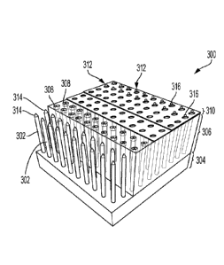
device having an array of diffractive patterns formed into a substrate;
[0015] FIG. 5B is a schematic diagram, in bottom view, of the example quantum
control
device of FIG. 5A;
[0016] FIG. 6A is a schematic diagram, in cross-section, of an example quantum
control
device having an array of lenses formed onto a substrate;
[0017] FIG. 6B is a schematic diagram, in bottom view, of the example quantum
control
device of FIG. 6A;
[0018] FIG. 7A is a schematic diagram, in cross-section, of an example quantum
control
device having a conductive layer that includes a plurality of voids;
2
CA 03131807 2021-08-27
WO 2020/181362 PCT/CA2020/050291
[0019] FIG. 7B is a schematic diagram, in bottom view, of the example quantum
control
device of FIG. 7A; and
[0020] FIG. 8 is a schematic diagram, in cross-section, of two instances of
the example
quantum control device of FIG. 3A, but in which the instances face each other
and share a
field-responsive layer in common.
DETAILED DESCRIPTION
[0021] In some aspects of what is described here, quantum control devices are
presented for interacting with quantum states using an electric field. In
particular, a
quantum control device may include a substrate having a substrate surface. An
insulator
layer is disposed over the substrate surface and defines a cavity. The
insulator layer
includes an insulator surface that defines an opening to the cavity. The
quantum control
device also includes a field-responsive layer over the insulator surface. The
field-
responsive layer includes a target region that resides over the opening to the
cavity. The
quantum control device additionally includes a projection extending from the
substrate
into the cavity and terminating at a tip. The projection is configured to
produce an electric
field that interacts with a quantum state in the target region. The tip
resides in the cavity
and is configured to concentrate the electric field produced by the
projection.
[0022] In some aspects of what is described here, a quantum control device may
include
a substrate and an insulator layer that defines an array of cavities. A field-
responsive layer
is disposed over the insulator layer and includes an array of target regions,
each aligned
with a corresponding cavity. The quantum control device may also include a
projection
extending from the substrate into a respective cavity. The projection is
configured to
produce an electric field that: [1] interacts with a quantum state of a target
region adjacent
the projection, and [2] controls quantum coupling between the quantum state of
the target
region and a quantum state of a neighboring target region. The array of
projections may
allow the quantum control device to correlate the quantum states of each
target region,
thereby establishing one or more collective quantum states.
[0023] Now referring to FIG. 1A, a schematic diagram is presented, in cross-
section, of
an example quantum control device 100 having a substrate 102 and a projection
104
3
CA 03131807 2021-08-27
WO 2020/181362 PCT/CA2020/050291
extending therefrom. The substrate 102 includes a substrate surface 106, which
may be a
planar surface, as shown in FIG. 1A. The substrate 102 may be formed of a
semiconductor
material such as silicon, germanium, a silicon-germanium alloy, and gallium
arsenide.
Other materials, however, are possible (e.g., insulator or metallic
materials). The
projection 104 extends from the substrate surface 106 into a cavity 108 and
may define a
pillar-shaped structure. However, other shapes are possible (e.g., pyramidal,
hemispherical, wedge-shaped, etc.). The projection 104 may be part of the
substrate 102,
as shown in FIG. 1A, or alternatively, be a separate structure coupled to the
substrate 102.
The projection 104 may be formed of the same material as the substrate 102 or
formed of a
material different than the substrate 102. For example, the projection 104 may
be formed
of a metallic material (e.g., Mo, W, Cu, etc.), a semiconductor material
(e.g., Si, Ge, Si-Ge
alloy, GaN, GaAs, etc.), a carbonaceous material (e.g., diamond, carbon
nanotubes, carbon
nanorods, etc.), or a ceramic material (e.g., hexagonal boron nitride,
metallic oxides, etc.).
Other materials are possible.
[0024] The example quantum control device 100 includes an insulator layer 110
disposed over the substrate surface 106 and defining the cavity 108. The
insulator layer
110 includes an insulator surface 112 that defines an opening 114 to the
cavity 108. The
insulator surface 112 may be a planar surface and may also be parallel to the
substrate
surface 106. The insulator layer 110 may be in contact with the substrate
surface 106, such
as shown in FIG. 1A, or alternatively, be coupled to the substrate 102 through
one or more
intermediate layers. Such intermediate layers may improve a coupling of the
insulator
layer 110 to the substrate 102.
[0025] In some implementations, the cavity 108 is disposed entirely through
the
insulator layer 110. In these implementations, the cavity 108 may be defined
by a
longitudinal axis and a cross-sectional area. The longitudinal axis may be
straight, curved,
or some combination thereof. The cross-sectional area may be bounded by any
type of
perimeter (e.g., a circle, a hexagon, an oblong, a parallelogram, etc.). The
cross-sectional
area may also remain constant along the longitudinal axis or vary with
distance through
the insulator layer 110. For example, the cavity 108 may be a cylindrical
cavity that is
defined by a straight longitudinal axis and a circular cross-sectional area of
constant radius.
4
CA 03131807 2021-08-27
WO 2020/181362 PCT/CA2020/050291
In another example, the cavity 108 may have a frustrum shape that is defined
by a straight
longitudinal axis and a cross-sectional area that decreases in size with
distance from the
insulator surface 112. Other shapes for the cavity 108 are possible.
[0026] In some implementations, the insulator layer 110 is formed of a
material having
an electrical resistivity equal to or greater than 1 x 10⁸ .cm. Examples of
such materials
include aluminum oxide (e.g., Al2O3), silicon oxide (e.g., S102, SiOx, etc.),
silicon nitride (e.g.,
S13N4), silicon oxynitride (e.g., SiOxNy), hafnium oxide (e.g., Hf02),
titanium nitride (e.g., TiN)
and so forth. In some implementations, the material has an electrical
resistivity equal to or
greater than 1 x 10100.cm at room temperature. In some implementations, the
material
has an electrical resistivity equal to or greater than 1 x 10¹² n=cm at room
temperature. In
some implementations the material has an electrical resistivity equal to or
greater than 1 x
1014 f2-cm at room temperature.
[0027] The example quantum control device 100 also includes a field-responsive
layer
116 disposed over the insulator surface 112 and including a target region 118.
The target
region 118 resides over the opening 114 to the cavity 108, which may be at a
position
centered over the opening 114 and opposite the projection 104. However, other
positions
of the target region 118 are possible (e.g., off-center, offset relative to
the projection 104,
etc.) In some instances, the field-responsive layer 116 is a patterned layer,
which may be
formed of two or more materials. In some instances, the field-responsive layer
116
includes a plurality of layers. The plurality of layers may include a
ferromagnetic layer, and
antiferromagnetic layer, a superconducting layer, or any combination thereof.
Other types
of layers are possible. Moreover, the plurality of layers may define a
sandwiched structure
having one or more of a ferromagnetic layer, an antiferTomagnetic layer, and a
superconducting layer sandwiched between other layers (e.g., ferromagnetic
layers,
antiferromagnetic layers, superconducting layers, etc.).
[0028] The field-responsive layer 116 may have one or more quantum states
associated
with the target region 118 that change in response to the electric field.
Examples of the one
or more quantum states include those based on an electronic band structure, an
electronic
spin, a nuclear spin, a magnetic ordering, a magnetic moment, a ferroelectric
ordering, a
ferroelectric moment, an atomic ordering, an optical transition, a phonon
dispersion, one
CA 03131807 2021-08-27
WO 2020/181362 PCT/CA2020/050291
or more discrete energy levels, and so forth. Other types of quantum states
are possible,
including those based on a superposition of quantum states and an entanglement
of
quantum states.
[0029] The target region 118 may include a feature in the atomic structure of
the field-
responsive layer 116 that allows the one or more quantum states to emerge
within the
target region 118, enhances an interaction between the one or more quantum
states and
the electric field, or both. The atomic structure may be a two-dimensional
atomic
structure, a three-dimensional atomic structure, an amorphous atomic
structure, or some
combination thereof. For example, the field-responsive layer 116 may include a
layer of
graphene, which corresponds to a two-dimensional atomic structure. Examples of
other
two-dimensional atomic structures include a layer of hexagonal boron nitride
(e.g., h-BN), a
layer of molybdenum sulfide (e.g., MoS2), and a layer of tungsten sulfide
(e.g., WS2). In
another example, the field-responsive layer 116 may include a three-
dimensional island
formed of diamond, such as on an exterior or interior surface of the field-
responsive layer
116. The three-dimensional island may also be partially or wholly embedded
within the
field responsive layer. In yet another example, the field-responsive layer 116
may include a
nanoparticle formed of metallic glass (e.g., gold, silver, an amorphous alloy
of iron and
boron). The metallic glass may have a magnetic moment.
[0030] In some implementations, the target region 118 includes an inclusion
in the
atomic structure of the field-responsive layer 116. The inclusion may result
from an atom
(or group of atoms) occupying an interstitial space in the atomic structure.
In some
implementations, the target region 118 includes a substitution in the atomic
structure of
the field-responsive layer 116. The substitution may result from a chemical or
isotopic
substitution of one or more atoms for others in the atomic structure. In some
implementations, the target region 118 includes a vacancy in the atomic
structure of the
field-responsive layer 116.
[0031] In some implementations, the target region 118 includes an atom or
molecule on
a surface of the field-responsive layer 116. The atom or molecule may include
a plurality of
atoms or molecules, and as such, may be an individual atom, a cluster of
atoms, a chemical
functional group, a nanoparticle, one or more molecules, a two-dimensional
island of atoms
6
CA 03131807 2021-08-27
WO 2020/181362 PCT/CA2020/050291
or molecules, a stacked heterostructure based on an ordered arrangement of
atom, a
patterned overlayer of atoms, and so forth. The atom or molecule may be
disposed on an
exterior surface, of the field-responsive layer 116. The atom or molecule may
also be
disposed on an interior surface of the field-responsive layer 116. In some
instances, both
the exterior surface and the interior surface of the field-responsive layer
116 have an atom
or molecule disposed thereon.
[0032] The example quantum control device 100 additionally includes the
projection
104, which terminates at a tip 120. In some variations, multiple instances of
the projection
104 may extend from the substrate 102 into the cavity 108 (i.e., a plurality
of projections
104). The projection 104 may have a height-to-width ratio in a range of 2:1 to
10000:1. In
some instances, the projection 104 may have a height-to-width ratio in a range
of 20:1 to
200:1. The projection 104 is configured to produce an electric field that
interacts with a
quantum state in the target region 118. The tip 120 resides in the cavity 108
and is
configured to concentrate the electric field produced by the projection 104.
In some
instances, the tip 120 is configured to concentrate the electric field to a
magnitude of at
least lx 105 V/m in the target region 118. In some instances, the tip 120 is
configured to
concentrate the electric field to a magnitude of at least 1 x 10⁹ V/m in the
target region 118.
In some instances, the tip 120 is configured to concentrate the electric field
to a magnitude
of at least 1 x 10¹⁰ V/m in the target region 118. In some instances, the tip
120 is
configured to concentrate the electric field to a magnitude of at least lx
1011V/m in the
target region 118. In some instances, the tip 120 is configured to concentrate
the electric
field to a magnitude of at least 1 x 10¹² V/m in the target region 118.
[0033] Concentration of the electric field may be aided by a shape of the tip
120 and a
placement of the tip 120 relative to the target region 118. For example, the
tip 120 may
have a conical shape whose narrowing taper allows the electric field to
emanate from a
substantially reduced surface. The tip 120 may also include one or both of a
textured
surface and a nanoparticle to help concentrate the electric field. The tip 120
may
additionally include a substructure, such as a grating coupler, to help
concentrate the
electric field. In another example, the tip 120 may reside in the cavity 108
less than 100
nm from the target region 118. Such placement may allow the target region 118
to
7
CA 03131807 2021-08-27
WO 2020/181362 PCT/CA2020/050291
experience a high of electric field (e.g., a magnitude at least 1 x 10⁵ Vim).
In some
instances, the tip 120 resides in the cavity 108 less than 20 nm from the
target region 118.
In some instances, the tip 120 resides in the cavity 108 less than 15 nm from
the target
region 118. In some instances, the tip 120 resides in the cavity 108 less than
10 nm from
the target region 118. In some instances, the tip 120 resides in the cavity
108 less than 5
nm from the target region 118. In some instances, the tip 120 resides in the
cavity 108 less
than 1 nm from the target region 118.
[0034] In some implementations, the projection 104 is formed of a material
resistant to
electron emission under high electric fields (or strong applied voltages). For
example, the
projection 104 may be formed of a material having a work function of at least
4.0 eV.
Examples of such materials include semiconductor materials (e.g., Si, Ge, and
Si-Ge alloys),
metallic materials (e.g., Mo, W, and Cu), ceramic materials (e.g., h-BN, W0x,
and Mo0x), and
carbonaceous materials (e.g., diamond, carbon nanotubes, and carbon nanorods).
In some
instances, the projection 104 is formed of a material having a work function
of at least 4.2
eV. In some instances, the projection 104 is formed of a material having a
work function of
at least 4.4 eV. In some instances, the projection 104 is formed of a material
having a work
function of at least 4.6 eV. In some instances, the projection 104 is formed
of a material
having a work function of at least 4.8 eV. In some instances, the projection
104 is formed of
a material having a work function of at least 5.0 eV.
[0035] When formed of a semiconductor material, the projection 104 may include
a
doping profile that defines a spatial distribution of p-type dopants, n-type
dopants, or both,
within the projection 104. The spatial distribution may be simple (e.g., a
uniform
distribution) or complex (e.g., a distribution establishing one or more p-n
junctions along
the projection 104). In some instances, the projection 104 is formed of a
conductive
material. The conductive material may have an electrical resistivity less than
100 SI-cm at
room temperature. For example, the conductive material may be a doped silicon
material
having a room-temperature electrical resistivity in the range of 2-50 .cm. In
further
instances, the conductive material may have an electrical resistivity less
than 1 x 10⁴ )cm.
In some variations, the projection 104 is formed of a material that becomes
conductive
when activated (e.g., when a voltage is applied to the projection 104). The
material may
8
CA 03131807 2021-08-27
WO 2020/181362 PCT/CA2020/050291
transition to an electrical resistivity below 100 L2-cm when activated. In
some instances,
the projection 104 may include a coated outer surface. For example, the
projection 104
may be formed of a first material (e.g. Si) and coated with a second material
(e.g., Pt) having
a higher work function than the first material. In some variations, the second
material may
be a superconducting material.
[0036] In some implementations, the substrate 102, the insulator layer 110,
and the
field-responsive layer 116 define an enclosed space 122 in the cavity 108
(e.g., see dashed
line in FIG. 1A). The enclosed space 122 includes a first clearance volume 124
between the
projection and the insulator layer. The first clearance volume 124 may include
a volume
between a side of the projection 104 and a side wall of the cavity 108. In
some instances,
the enclosed space 122 may also include a second clearance volume 126 between
the
projection 104 and the field-responsive layer 116. The second clearance volume
126 may
include a volume between a tip 120 of the projection 104 and an interior
surface of the
field-responsive layer 116. The enclosed space 122 is operable to electrically
isolate the
projection 104 from the insulator layer 110. The enclosed space 122 may also
assist the
insulator layer 110 in electrically-isolating the projection 104 from other
projections in
respective cavities of the insulator layer 110 (e.gõ if the quantum control
device is part of
an array of quantum control devices).
[0037] The enclosed space 122 may include a vacuum in any portion thereof,
including
an entire portion. In some instances, the enclosed space 122 contains a vacuum
pressure
no greater than 10-5 Torr. In some instances, the enclosed space 122 contains
a vacuum
pressure no greater than 10-8 Torr. The enclosed space 122 may also be filled
at least
partially with a dielectric material. Such filling may partition the enclosed
space 122 into
one or more internal chambers, or alternatively, filled the enclosed space 122
entirely. FIG.
113 presents a schematic diagram of the example quantum control device 100 of
FIG. 1A,
but in which the enclosed space 122 is entirely filled by dielectric material.
The dielectric
material may be a material having a dielectric constant ranging from 1 to 10.
In some
instances, the dielectric material has a dielectric constant greater than 10.
In some
instances, the dielectric material has a dielectric constant greater than 100.
The dielectric
material may also have a dielectric strength greater than 0.05 V/nm, and in
many
9
CA 03131807 2021-08-27
WO 2020/181362 PCT/CA2020/050291
variations, greater than 1 V/nm. Examples of such materials include silicon
oxide (e.g.,
SiO2), silicon nitride (e.g., Si3N4), boron nitride (e.g. h-BN), and diamond.
In some instances,
the dielectric material may be formed of the same material as the insulator
layer 110.
[0038] In some implementations, the insulator layer 110 includes an
interior sidewall
134 surrounding the projection 104 that defines at least a portion of the
cavity 108. The
interior sidewall 134 may meet the insulator surface 112 at the opening 114 to
the cavity
108. In some instances, the interior sidewall 134 is displaced from the
projection 104 to
create a gap (e.g., see FIGS. 1A-1C). The gap may contribute to the first
clearance volume
124 of the projection 104. In some instances, the interior sidewall 134 may
contact the
projection 104 along at least a portion of a surface of the projection 104.
Such contact may
embed the projection 104 within the insulator layer 110.
[0039] In further implementations, the opening 114 is a first opening 114 of
the cavity
108 and the insulator surface 112 is a first insulator surface 112 of the
insulator layer 110.
The insulator layer 110 includes a second insulator surface 136 coupled to the
substrate
surface 106 and opposite the first insulator surface 112. Such coupling may
include direct
contact between the second insulator surface 136 and the substrate surface
106, or
alternatively, occur through one or more intermediate layers. The one or more
intermediate layers may improve a coupling of the insulator layer 110 to the
substrate 102.
In some instances, the substrate surface 106, the first insulator surface 112
and the second
insulator surface 136 are planar surfaces. In these embodiments, the interior
sidewall 134
extends through a thickness of the insulator layer 110 and meets the second
insulator
surface 106 at a second opening 138 of the cavity 108. The projection 104
extends from
the substrate 102 through the second opening 138 of the cavity 108 and extends
to a height
from the substrate 102 that is less than the thickness of the insulator layer
110.
[0040] The example quantum control device 100 may include an addressing layer
128
below the substrate 102 that includes an electrical contact 130 opposite a
base 132 of the
projection 104. The addressing layer 128 may be in contact with the substrate
102, such as
shown in FIG 1A, or alternatively, be coupled to the substrate 102 through one
or more
intermediate layers. Such intermediate layers may improve a coupling of the
addressing
layer 128 to the substrate 102. The electrical contact 130 may be configured
to deliver a
CA 03131807 2021-08-27
WO 2020/181362 PCT/CA2020/050291
voltage to the substrate 102. The electrical contact 130 may also be
configured to receive
an electrical signal from the substrate 102 that represents a quantum state of
the target
region 118. In this capacity, the electrical contact 130 may be used to
characterize a
quantum state of the target region 118.
[0041] In implementations having the addressing layer 128, the substrate 102
may be
configured to transfer the voltage to the projection 104 to produce the
electric field and
transfer the electrical signal from the projection 104 to the electrical
contact 130. A voltage
potential of the substrate 102 may be controlled independently of a voltage
potential of the
tip 120 of the projection 104. Such independent control may be assisted by the
addressing
layer 128 and the electrical contact 130.
[0042] In operation, the example quantum control device 100 experiences a
voltage
potential between the substrate 102 (or electrical contact 130, if present)
and the field-
responsive layer 116 (or a layer above). In particular, a voltage may be
applied to the
substrate 102 (or electrical contact 130), which then transfers to the
projection 104 to
establish the voltage potential. The voltage may be applied continuously or
through
voltage pulses. The voltage pulses may have a time duration less than or equal
to 1
millisecond. In some instances, the time duration is less than or equal to 1
picosecond. In
some instances, the time duration is less than or equal to 100 femtoseconds
(e.g., 10-40
femtoseconds).
[0043] The voltage may be supplemented by a laser to establish the voltage
potential.
For example, the laser may generate a coherent beam of elect' magnetic
radiation that is
received by the target region 118, the projection 104 (or multiple instances
thereof), or
both. Upon receipt, an electric field component of the coherent beam of
electromagnetic
radiation may alter the voltage potential (e.g., increase the voltage
potential) between the
projection 104 (or multiple instances thereof) and the target region 118. The
voltage
potential may include pulses having a time duration. In some instances, the
time duration
of the pulses is less than or equal to 1 picosecond. In some instances, the
time duration of
the pulses is less than or equal to 100 femtoseconds (e.g., 10-40
femtoseconds).
11
CA 03131807 2021-08-27
WO 2020/181362 PCT/CA2020/050291
[0044] In response, the electric field is generated, during which, the
electric field
extends from the tip 120 of the projection 104 to penetrate the target region
118. The tip
120 functions, in part, to concentrate the electric field to high magnitudes,
and as such, the
target region 118 may receive the electric field at a magnitude of at least 1
x 105 V/m. In
many instances, the magnitude is greater than 1 x 10⁹ V/m. Upon receiving the
electric
field, the one or more quantum states of the target region 118 may emerge or
be altered in
characteristic (e.g., altered in number, occupancy, spin, energy, size,
spatial distribution,
coupling to other quantum states, etc.). In this manner, the voltage potential
may allow
manipulation of the one or more quantum states of the target region 118, and
in some
instances, may also allow manipulation of quantum states of the field-
responsive layer 116.
[0045] Control of the electric field - such as by altering a magnitude or
frequency of the
voltage, or by applying voltage pulses - may allow for interaction with the
one or more
quantum states. Such interaction may change a property of the target region
118 (or field-
responsive layer 116) and allow for storing and manipulating information
represented by
the one or more quantum states. Examples of such properties include an optical
property
(e.g., an optical transmission, an optical reflection, an optical emission, a
polarization, a
phase, etc.), a magnetic property (e.g., a magnetic moment, a magnetic
ordering, an
inductance, etc.), a thermal property (e.g., a specific heat, a thermal
conductance, etc.), an
electrical property (e.g., a resistivity, a capacitance, etc.), and
combinations thereof (e.g., an
optoelectronic effect, a magnetocaloric effect, etc.). Other properties are
possible, such
quantum properties based on a correlation of two or more quantum states.
[0046] In some implementations, control of the electric field may establish an
electrostatic potential well in the target region 118 that results in the one
or more quantum
states each having a plurality of discrete energy levels. The plurality of
discrete energy
levels may be manipulated by the electric field to induce the target region
118 to function
as an artificial atom. In this capacity, the target region 118 may include a
discrete number
of electrons that populate a corresponding discrete spectrum of energy levels.
As such, the
target region 118 may operate analogously to an atom having an effective
nuclear charge
controlled by the electric field. Such operation may be allowed, controlled,
or enhanced by
12
a quantum system on the surface of the target region 118, or alternatively,
embedded in the
target region 118 (e.g., an inclusion). The quantum system may include an
individual atom,
a cluster of atoms, a chemical functional group, a nanopaiticle, one or more
molecules, a
two-dimensional island of atoms or molecules, a stacked heterostructure based
on an
ordered arrangement of atoms, a patterned overlayer of atoms, and so forth. In
some
instances, the electric field may induce the target region 118 to operate as a
Rydberg atom.
In these instances, one or more of electrons of the target region 118 may be
excited to high
energies, creating an artificial atom that has a high principal quantum
number.
[0047] In some implementations, control of the electric field may be used to
manipulate
a quantum system on the surface of the target region 118 (e.g., control a
position, change
an order or configuration, alter a quantum state, etc.). The quantum system
may include an
individual atom, a cluster of atoms, a chemical functional group, a
nanoparticle, one or
more molecules, a two-dimensional island of atoms or molecules, a stacked
heterostructure
based on an ordered arrangement of atoms, a patterned over layer of atoms, and
so forth
The quantum system may have quantum states, each having a plurality of
discrete energy
levels. Moreover, the target region 118 may include a discrete number of
electrons that
populate a corresponding discrete spectrum of energy levels associated with
the quantum
system. In these instances, one or more of electrons of the target region 118
may be
excited to high energies, creating an atom (or artificial atom) that has a
high principal
quantum number. In some instances, the quantum system includes a Rydberg atom
(e.g.,
an ionized Cs atom), molecules with Rydberg-like states (e.g., homopolar
diatomic
molecules such as H2, P2, C12, acetylene, etc.), or matter with Rydberg-like
states on the
surface of the target region 118.
[0048] In some implementations, the field-responsive layer 116 includes a
plurality of
layers that comprises a target layer 140 and an intermediate layer 142, as
shown in FIG. 1C.
The target layer 140 contains the target region 118 and the intermediate layer
142 is
disposed between the insulator layer 110 and the target layer 140. A thickness
144 of the
intermediate layer 142 is part of a distance 146 between the tip 120 of the
projection 104
and the target region 118 of the field-responsive layer 116. The distance 146
may be less
13
Date Recue/Date Received 2023-04-13
CA 03131807 2021-08-27
WO 2020/181362 PCT/CA2020/050291
than 100 nm. In some instances, the distance 146 is less than 20 nm from the
target region
118. In some instances, the distance 146 is less than 15 nm from the target
region 118. In
some instances, the distance 146 is less than 10 nm from the target region
118. In some
instances, the distance 146 is less than 5 nm from the target region 118. In
some instances,
the distance 146 is less than 1 nm from the target region 118.
[0049] In some implementations, the insulator layer 110 includes a first
insulator layer
over the substrate surface 106 and a second insulator layer between the first
insulator
layer and the field-responsive layer 116, In some implementations, the example
quantum
control device 100 includes a second insulator layer over the field-responsive
layer 116.
The second insulator layer may include a hole opposite the opening 114 of the
cavity 108.
In further implementations, the example quantum control device 100 includes a
conductive
layer over the second insulator layer. The hole of the second insulator layer
may propagate
through the conductive layer.
[0050] The example quantum control device 100 may utilize optical stimulation
of the
projection 104 to generate, or assist in generating the electric field. In
some
implementations, the substrate surface 106 is a first substrate surface and
the substrate
102 includes a second substrate surface opposite the first substrate surface.
The first
substrate surface, the second substrate surface, and the insulator surface (or
first insulator
surface) are planar surfaces. The substrate also includes an optical focusing
structure
formed on the second substrate surface opposite the base 132 of the projection
104. The
optical focusing structure is configured to guide light to the projection 104.
Examples of
the optical focusing structure include a diffractive pattern formed on the
second substrate
and a lens formed on the substrate surface. These structures may be defined by
the second
substrate surface, or alternatively, be defined by a distinct structure
coupled to the second
substrate surface.
[0051] The example quantum control device 100 may also utilize optical
stimulation of
the target region 118 to assist the projection 104 in generating the electric
field. In some
implementations, the target region 118 of the field-responsive layer 116
includes a
nanoparticle disposed thereon. The nanoparticle may be operable to enhance an
electric-
14
CA 03131807 2021-08-27
WO 2020/181362 PCT/CA2020/050291
field component associated with a beam of light (e.g., laser light) that
impinges upon the
target region 118. The enhanced electric-field component may add to a
magnitude of the
electric field generated by the projection 104. The nanoparticle may be
disposed on an
interior surface or an exterior surface of the field-responsive layer 116. In
some instances,
the target region 118 is embedded within the field-responsive layer 116 along
with the
nanoparticle. In these instances, the nanoparticle and target region 118 may
define an
inclusion in the field-responsive layer 116.
[0052] In some implementations, the example quantum control device 100
includes a
laser configured to direct a beam of light onto the target region 118. The
beam of light may
include one or more types of laser beams. The beam of light may also include
one or more
frequencies of electromagnetic radiation (e.g., frequencies of ultraviolet
light). The laser
may be operable to eject one or more electrons from the target region 118 by
processes of
photoemission. The example quantum control device 100 also includes an
electron
spectrometer configured to receive electrons emitted from the target region
118 in
response to receiving the beam of light. The electron spectrometer may be able
to
determine characteristics of the one or more quantum states of the target
region 118 by
measuring properties of the electrons (e.g., an energy of the electrons). In
further
implementations, the example quantum control device 100 may include an optical
spectrometer configured to determine characteristics of one or more quantum
states of the
target region 118 by measuring properties of photons.
[0053] In some implementations, the example quantum control device 100 is
configured to operate in a cryogenic environment. For example, the example
quantum
control device 100 may be disposed within a cryostat. The cryogenic
environment may
have any temperature below about 123 K (e.g., 77 K, 4 K, less than 1 K, etc.).
In some
implementations, the example quantum control device 100 is configured to
operate in a
vacuum environment. For example, the example quantum control device 100 may be
disposed in a sealable vacuum chamber coupled to one or more vacuum pumps
(e.g, rotary
vane pumps, turbomolecular pumps, cryogenic pumps, etc.). The vacuum
environment
may be any partial pressure of gas below 10-1 torr (e.g., 10-3 torr, 10-6
torr, 10 torr, etc.).
CA 03131807 2021-08-27
WO 2020/181362 PCT/CA2020/050291
In some implementations, the example quantum control device 100 is configured
to
operate in a magnetic field (i.e., For example, the example quantum control
device may
be disposed in a magnetic field of a superconducting coil. The magnetic field
may be an
applied magnetic field greater than 10 mT. In some variations, the applied
magnetic field is
greater than 100 mT (e.g., 300 mT). In some variations, the applied magnetic
field is
greater than 500 mT (e.g., 1 T, 3 T, 4 T, etc.).
[0054] FIG. 2A presents four contour plots 200, 202, 204, 206 showing the
simulated
influence of an electric field on an example 200-nm graphene flake having
armchair
boundaries. The four contour plots are generated from a computer simulation of
the
electric field on the example 200-nm graphene flake using a Pybinding library.
A density of
states of the example 200-nm graphene flake is shown to respond to the
electric field,
which increases sequentially from contour plot 200 to contour plot 206. A
magnitude of
the electric field is represented by /3, which increases from 0.0, to 0.4, to
0.8, and to 1.2
when going, respectively, from contour plot 200, to contour plot 202, to
contour plot 204,
and to contour plot 206. The density of states is represented in FIG. 2A by
shades of gray,
which form the basis for the contours of each contour plot. Grayscale legends
to the right
of FIG. 2A match each shade of gray with a corresponding magnitude of the
density of
states. The density of states in the grayscale legends ranges from 10-3 to 10-
1 eV-1=nm-2.
[0055] The abscissa of each contour plot shows a distance, in nanometers, from
a center
(i.e., r = 0 nm) of the example 200-nm graphene flake. The example 200-nm
graphene flake
may define a field-responsive layer, such as the field-responsive layer 116
described in
relation to FIGS. 1A-1C. A portion of the example 200-nm graphene flake at or
immediately
adjacent of the center may also define a target region, such as the target
region 118
described in relation to FIGS. 1A-1C. The ordinate of each contour plot shows
an energy
level, in electron-volts (eV), that may be associated with an energy of the
density of states.
A dashed line 208 indicates a band profile for electrons that responds to the
presence of
the electric field. For non-zero electric fields (i.e., 13 > 0), the band
profile may define an
electrostatic potential well around the center of the 200-nm graphene flake
(or the target
region thereof), as will be described in relation to contour plots 200, 202,
204, 206.
16
CA 03131807 2021-08-27
WO 2020/181362 PCT/CA2020/050291
[0056] As shown by contour plot 200, the density of states at/3 = 0 is
constant when
traversing a horizontal distance from r = -30 nm to r = 30 nm. A band interval
with a low
density of states (e.g., about 10-3 eV-1-nm-2 or less) straddles the energy
level of 0 eV from r
= -30 nm to r = 30 nm. In contour plot 200, no electric field is present
(i.e., fl = 0) and the
dashed line 208 is a horizontal along an energy level of about 0 eV. However,
the presence
of an electric field (i.e., > 0) can alter a profile of this band interval and
form an
electrostatic potential well. The electric field may be generated by one or
more sources.
For example, a projection (or tip thereof) may reside adjacent of the center
of example 200-
nm graphene flake. A voltage applied to the projection (or tip thereof)
establishes a voltage
potential relative to the example 200-nm graphene flake. This voltage
potential may cause
an electric field to emanate from the projection (or tip thereof) towards the
center of the
example 200-nm graphene flake. Other examples of the source include an
inclusion in an
atomic structure of the example 200-nm graphene flake, a substitution in an
atomic
structure of the example 200-nm graphene flake, a vacancy in an atomic
structure of the
example 200-nm graphene flake, and an atom or molecule on a surface of the
example 200-
nm graphene flake.
[0057] At (1 = 0.4, the electric field (or voltage) alters the profile of the
band interval and
induces the formation of the electrostatic potential well, as shown by contour
plot 202. The
electric field also increases the density of states at approximately r = 0 nm,
which is
concentrated at energy levels at or above 0 eV. The density of states at
approximately r = 0
nm corresponds to a local density of states. Increasing the electric field to
fl = 0.8 widens
the electrostatic potential well and increases its bending, as shown by
contour plot 204.
The local density of states continues to increase in magnitude and extends to
energy levels
below 0 eV. At f3 = 1.2, the local density of states has increased notably in
magnitude,
especially at energy levels below 0 eV as shown by contour plot 206. It will
be appreciated
that the electric field (or voltage), by inducing the formation of the
electrostatic potential
well and increasing the local density of states, may confine one or more
electrons in the
target region of the example 200-nm graphene flake. Such localization of
electrons may
allow the target region to have quantum states that can be controlled by one
or both of the
electric field and a magnetic field.
17
CA 03131807 2021-08-27
WO 2020/181362 PCT/CA2020/050291
[0058] For example, the presence of a magnetic field may cause the local
density of
states to split into a plurality of discrete energy levels (or Landau levels)
that can define
one or more quantum states. The one or more quantum states may be associated
with the
target region of the 200-nm graphene flake. FIG. 28 presents four contour
plots 210, 212,
214, 216 showing the simulated influence of an electric field and a 12 T
magnetic field on
an example 200-nm graphene flake having armchair boundaries. The four contour
plots
are generated from a computer simulation of the electric and 12 T magnetic
fields on the
example 200-nm graphene flake using a Pybinding library. The contour plots
210, 212,
214, 216 are analogous to the contour plots 200, 202, 204, 206 of FIG. 2A,
except that the
example 200-nm graphene flake is simulated in the further presence of the 12 T
magnetic
field. For fl = 0, the density of states is again constant when traversing the
horizontal
distance from r = -30 nm to r = 30 nm. However, the presence of the 12 T
magnetic field
causes two band intervals to emerge where only one was present with no
magnetic field
(compare to contour plot 200 of FIG. 2A), In particular, a first band interval
resides below
0 eV and a second band interval resides above 0 eV. The first and second band
intervals are
separated by a narrow band interval at approximately 0 eV having a density of
states of
about 10-2 eV-I-nm-2. The dashed line 208 is a horizontal along an energy
level of about 0
eV and disposed within the narrow band interval.
[0059] At 13 = 0.4, the electric field (or voltage) alters the profile of
the first band
interval, the second band interval, and the narrow band interval, and induces
the formation
of the electrostatic potential well, as shown by contour plot 212. The
electric field also
increases a magnitude of the local density of states (i.e., at approximately r
= 0 nm), which
is concentrated at energy levels above the second band interval. Increasing
the electric
field to fi = 0.8 causes a splitting of the narrow band interval into two
portions, one portion
in the first band interval and one portion in the second band interval as
shown by contour
plot 214. Increasing the electric field also widens the electrostatic
potential well and
increases its bending. The local density of states continues to increase in
magnitude and
extends to energy levels below 0 eV. Moreover, the local density of states is
split into a
plurality of discrete energy levels 218, which may correspond to Landau
levels. The
plurality of discrete energy levels 218 may define one or more quantum states.
Further
18
CA 03131807 2021-08-27
WO 2020/181362 PCT/CA2020/050291
increasing the electric field to f3 = 1.2 may cause additional splitting of
the plurality of
discrete energy levels 218. However, the increased electric field may also
increase the
magnitude of the local density of states, especially at energy levels below 0
eV, as shown by
contour plot 216. The increased local density of states may allow one or more
electrons to
become increasingly confined at the target region of the example 200-nm
graphene flake.
[0060] As shown by contour plots 210, 212, 214, and 216, control of the
electric field
allows the localization of electrons within the target region of the example
200-nm
graphene flake. But due to the presence of the 12 T magnetic field, such
control also allows
the localized electrons to be distributed among the plurality of discrete
energy levels 218.
The electrons, the plurality of discrete energy levels 218, or both may be
manipulated by
altering a magnitude of the electric field, which may manipulate respective
quantum states
of the electrons and the plurality of discrete energy levels 218. Such
manipulation may
allow a property of the target region (or the example 200-nm graphene flake)
to be created
or altered. Such manipulation may also allow for storing and manipulating
information
represented by the quantum states. Although the contour plots 210, 212,
214,216 present
the simulation in the context of a constant magnetic field, the magnetic field
may also be
altered in magnitude to manipulate one or both of the electrons and the
plurality of
discrete energy levels 218.
[0061] Now referring back to FIGS. 1A-1C, in some implementations, the example
quantum control device 100 includes an optical waveguide associated with the
target
region 118. The optical waveguide may be defined by the insulator layer 110
(or a portion
thereof), the field-responsive layer 116 (or a portion thereof), the cavity
108 (or a portion
thereof), or any combination thereof. In some instances, the optical waveguide
may
include one or more sublayers of the insulator layer 110, one or more
sublayers of the
field-responsive layer 116, or both. The optical waveguide may be configured
to propagate
photons in-plane within one or both of the insulator layer 110 and the field-
responsive
layer 116. The optical waveguide may also be configured to propagate photons
out-of-
plane of the insulator layer 110 or the field-responsive layer 116. For
example, the optical
waveguide may include surfaces associated with the cavity 108 - e.g., an end
surface, a
19
CA 03131807 2021-08-27
WO 2020/181362 PCT/CA2020/050291
sidewall surface, and so forth ¨ that allow reflection of the photons along a
longitudinal axis
of the projection 104 (or plurality of projections).
[0062] The optical waveguide may have an active volume for propagating (or
resonating) photons therein. These photons may be frequency-shaped or pulse-
shaped to
optimize a nature and a purity of desired, discrete quantum states. The
photons may have
wavelengths that correspond to microwave wavelengths, infrared wavelengths,
visible
light wavelengths, or ultraviolet wavelengths. Other wavelengths are possible.
During
operation, photons within the active volume may couple to a quantum state of
the target
region 118 associated with the optical waveguide. The optical waveguide may
thus be used
to select or control a quantum state of the target region 118. The optical
waveguide may
also be used to induce a new quantum state in the target region 118. Coupling
between the
photons and the quantum state may modify an energy of the quantum state. Such
coupling
may also establish a quantum system whose behavior is governed by cavity
quantum
electrodynamics.
[0063] A quantum control method may be used to operate the quantum control
device
100 described in relation to FIGS. 1A-1C, according to an illustrative
example. The
quantum control method includes generating an electric field from a projection
on a
substrate. The projection extends from a substrate surface of the substrate
into a cavity
defined by an insulator layer. Moreover, the insulator layer is disposed over
the substrate
surface and comprises an insulator surface that defines an opening to the
cavity. The
quantum control method also includes receiving the electric field at a target
region of a
field-responsive layer. The field-responsive layer is disposed over the
insulating layer, and
the target region resides over the opening of the cavity. The quantum control
method
additional includes controlling the electric field to interact with a quantum
state in the
target region of the field-responsive layer. In some instances, the quantum
control method
includes transferring no electrons from the projection to the target region of
the field-
responsive layer while generating the electric field. In some instances, the
quantum
control method includes transferring an electron from the projection to the
target region of
the field-responsive layer while generating the electric field.
CA 03131807 2021-08-27
WO 2020/181362 PCT/CA2020/050291
[0064] In some implementations, generating the electric field at the
projection includes
concentrating the electric field with a tip of the projection. In these
implementations,
receiving the electric field at the target region includes receiving the
concentrated electric
field at the target region. The concentrated electric field may have a
magnitude of at least 1
x 105 V/m. In some instances, the concentrated electric field has a magnitude
of at least 1 x
109 V/m. In some instances, the concentrated electric field has a magnitude of
at least 1 x
1010 V/m. In some instances, the concentrated electric field has a magnitude
of at least lx
1011 V/m. In some instances, the concentrated electric field has a magnitude
of at least 1 x
1012 Vim
[0065] In some implementations, generating the electric field from the
projection
includes applying a voltage to an electrical contact below the substrate and
opposite a base
of the projection. Generating the electric field from the projection also
includes
transferring the voltage through the substrate to the projection. In some
implementations,
the quantum control method includes transferring an electrical signal from the
projection
to an electrical contact below the substrate and opposite a base of the
projection. The
electrical signal can be used to characterize the quantum state of the target
region.
[0066] In some implementations, the substrate surface is a first substrate
surface and
the substrate includes a second substrate surface opposite the first substrate
surface. In
these implementations, generating the electric field from the projection
includes receiving
a beam of light at an optical focusing structure opposite a base of the
projection. The
optical focusing structure is formed on the second substrate surface.
Generating the
electric field from the projection also includes guiding light to the
projection with the
optical focusing structure.
[0067] In some implementations, the quantum control method includes receiving
a
beam of light at the target region of the field-responsive layer. For example,
the beam of
light may be received by a nanoparticle disposed on a metallic surface of the
field-
responsive layer. The nanoparticle and metallic surface may define an
inclusion in the
target region of the field-responsive layer. In another example, the beam of
light may eject
one or more electrons from the target region by processes of photoemission. In
further
21
CA 03131807 2021-08-27
WO 2020/181362 PCT/CA2020/050291
implementations, the quantum control method includes receiving, at an electron
spectrometer, electrons emitted from the target region in response to the beam
of light.
[0068] In some implementations, controlling the electric field to interact
with the
quantum state includes altering a magnitude of the electric field to alter the
quantum state
in the target region of the field-responsive layer.
[0069] In some implementations, the tip resides in the cavity less than 100 nm
from the
target region. In some implementations, the tip resides in the cavity less
than 20 nm from
the target region. In some implementations, the tip resides in the cavity less
than 15 nm
from the target region. In some implementations, the tip resides in the cavity
less than 10
nm from the target region. In some implementations, the tip resides in the
cavity less than
nm from the target region. In some implementations, the tip resides in the
cavity less
than 1 nm from the target region.
[0070] In some implementations, the projection is formed of a material having
a work
function at least 4.0 eV. In some implementations, the projection is formed of
a material
having a work function at least 4.2 eV. In some implementations, the
projection is formed
of a material having a work function at least 4.4 eV. In some implementations,
the
projection is formed of a material having a work function at least 4.6 eV. In
some
implementations, the projection is formed of a material having a work function
at least 4.8
eV. In some implementations, the projection is formed of a material having a
work function
at least 5.0 eV. In some implementations, the projection has a height-to-width
ratio in a
range of 2:1 to 10000:1. In some implementations, the projection has a height-
to-width
ratio in a range of 20:1 to 200:1.
[0071] In some implementations, the target region includes an inclusion in an
atomic
structure of the field-responsive layer. In some implementations, the target
region includes
a substitution in an atomic structure of the field-responsive layer. In some
implementations, the target region includes a vacancy in an atomic structure
of the field-
responsive layer. In some implementations, the target region includes an atom
or molecule
on a surface of the field-responsive layer. The atom or molecule may include a
plurality of
22
CA 03131807 2021-08-27
WO 2020/181362 PCT/CA2020/050291
atoms or molecules, and as such, may be an individual atom, a cluster of
atoms, a chemical
functional group, a nanoparticle, one or more molecules, a two-dimensional
island of atoms
or molecules, a stacked heterostructure based on an ordered arrangement of
atom, a
patterned overlayer of atoms, and so forth. The atom or molecule may be
disposed on an
exterior surface of the field-responsive layer. The atom or molecule may also
be disposed
on an interior surface of the field-responsive layer. In some instances, both
the exterior
and interior surfaces of the field-responsive layer have an atom or molecule
disposed
thereon.
[0072] Now referring to FIG. 3A, a schematic diagram is presented, in
perspective view,
of an example quantum control device 300 that includes a plurality of
projections 302
disposed on a substrate 304. Certain features of the example quantum control
device 300
have portions omitted to allow other features to be visible in FIG. 3A. FIG.
3B presents a
schematic diagram, in cross-section, of the example quantum control device 300
of FIG. 3A.
One or more of plurality of projections in FIGS. 3A and 3B may be associated
with
individual instances of the example quantum control device 100 described in
relation to
FIGS. 1A-1C.
[0073] The example quantum control device 300 includes the substrate 304 and
an
insulator layer 306 that defines an array of cavities 308. The example quantum
control
device 300 also includes a field-responsive layer 310 that is disposed over
the insulator
layer 306 and includes an array of target regions 312. In FIGS. 3A & 3B, the
field-
responsive layer 310 is depicted as having two layers. However, other numbers
of layers
are possible for the field-responsive layer 310 (e.g., 1, 5, etc.). Each
target region 312 is
aligned with a corresponding cavity 308. Projections 302 extend from the
substrate 304
into respective cavities 308 and each is configured to produce an electric
field. The electric
field interacts with a quantum state of a target region adjacent the
projection and controls
quantum coupling between the quantum state of the target region and a quantum
state of a
neighboring target region.
[0074] In many implementations, the plurality of projections 302 defines a two-
dimensional array. For example, as shown in FIG. 4A, a plurality of
projections 400 may
23
CA 03131807 2021-08-27
WO 2020/181362 PCT/CA2020/050291
extend from a substrate 402 to define a rectilinear array 404. One projection
400 is
associated with each respective cavity 406 in an insulator layer 408. In
another example,
as shown in FIG. 4B, a plurality of projections 420 may extend from a
substrate 422 to
define a hexagonal array 424. One projection 420 is associated with each
respective cavity
426 in an insulator layer 428.
[0075] The plurality of projections 302 may also define a two-dimensional
array
different than that defined by the array of cavities 308. In some
implementations, at least
one projection 302 includes a subset of projections 302, each producing a
respective
electric field that defines part of the electric field. For example, as shown
in FIG. 4C, a
plurality of projection subsets 440 may define a rectilinear array 442. Each
projection
subset 440 is associated with a corresponding cavity 444 in an insulator layer
446 and has
five projections 448 that extend from a substrate 450 into the corresponding
cavity 444.
However, other numbers and arrangements of projections are possible for each
projection
subset 440. Moreover, the projection subsets 440 may define a two-dimensional
array
other than a rectilinear array.
[0076] The plurality of projections 302 may be ordered to determine a distance
between neighboring target regions 312. In some implementations, the distance
may be
less than or equal to 10 m. The distance may be the same for all neighboring
target
regions 312. For example, a distance between neighboring target regions 312
may be less
than or equal to 1000 nm for all neighboring target regions 312. The distance
may also be
different between portions of neighboring target regions 312. For example, the
neighboring target regions 312 may include a first portion having a distance
equal to or
less than 700 nm and a second portion having a distance equal to or less than
300 nm.
Other combinations of portions and distances are possible.
[0077] In some instances, a distance between neighboring target regions 312 is
less
than or equal to 1000 nm. In some instances, a distance between neighboring
target
regions 312 is less than or equal to 900 nm. In some instances, a distance
between
neighboring target regions 312 is less than or equal to 800 nm. In some
instances, a
distance between neighboring target regions 312 is less than or equal to 700
nm. In some
24
CA 03131807 2021-08-27
WO 2020/181362 PCT/CA2020/050291
instances, a distance between neighboring target regions 312 is less than or
equal to 600
rim. In some instances, a distance between neighboring target regions 312 is
less than or
equal to 500 nm. In some instances, a distance between neighboring target
regions 312 is
less than or equal to 400 nm. In some instances, a distance between
neighboring target
regions 312 is less than or equal to 300 nm. In some instances, a distance
between
neighboring target regions 312 is less than or equal to 200 nm.
[0078] Each projection 302 may have a height-to-width ratio in the range of
2:1 to
10000:1. In some instances, each projection 302 has a height-to-width ratio in
a range of
20:1 to 200:1. Each projection 302 may also be formed of a material having a
work
function of at least 4.0 eV. In some instances, each projection 302 is formed
of a material
having a work function of at least 4.2 eV. In some instances, each projection
302 is formed
of a material having a work function of at least 4.4 eV. In some instances,
each projection
302 is formed of a material having a work function of at least 4.6 eV. In some
instances,
each projection 302 is formed of a material having a work function of at least
4.8 eV. In
some instances, each projection 302 is formed of a material having a work
function of at
least 5.0 eV.
[0079] Each projection 302 may also terminate at a tip 314 that resides in
the
respective cavity 308. The tip 314 may end at a distance from the target
region 312
adjacent the projection 302. In many variations, the distance is the same for
all tips 314
associated with the plurality of projections 302. In some instances, the tip
314 resides in
the respective cavity 308 less than 100 nm from the adjacent target region
312. In some
instances, the tip 314 resides in the respective cavity 308 less than 20 nm
from the
adjacent target region 312. In some instances, the tip 314 resides in the
respective cavity
308 less than 15 nm from the adjacent target region 312. In some instances,
the tip 314
resides in the respective cavity 308 less than 10 nm from the adjacent target
region 312. In
some instances, the tip 314 resides in the respective cavity 308 less than 5
nrn from the
adjacent target region 312. In some instances, the tip 314 resides in the
respective cavity
308 less than 1 nm from the adjacent target region 312.
CA 03131807 2021-08-27
WO 2020/181362 PCT/CA2020/050291
[0080] In some implementations, each projection 302 terminates in a tip
configured to
concentrate the electric field produced by the projection. The tip may be
configured to
concentrate the electric field to a magnitude of at least 1 x 10⁵ V/m in the
target region
adjacent the projection. In some instances, the tip is configured to
concentrate the electric
field to a magnitude of at least 1 x 10⁸ V/m in the target region adjacent the
projection. In
some instances, the tip is configured to concentrate the electric field to a
magnitude of at
least 1 x 10¹⁰ V/m in the target region adjacent the projection. In some
instances, the tip is
configured to concentrate the electric field to a magnitude of at least 1 x
1011 V/m in the
target region adjacent the projection. In some instances, the tip is
configured to
concentrate the electric field to a magnitude of at least 1 x 10¹² V/m in the
target region
adjacent the projection.
[0081] In some implementations, the substrate 304, the insulator layer 306,
and the
field-responsive layer 310 define an enclosed space in each cavity 308. The
enclosed space
includes a first clearance volume between a respective projection 302 and the
insulator
layer 306. In some variations, the enclosed space may also include a second
clearance
volume between a tip of the respective projection 302 and field-responsive
layer 310. The
enclosed space may contain a vacuum pressure no greater than 10-5 Torr. In
some
instances, the enclosed space contains a vacuum pressure no greater than 10-8
Torr. In
some instances, the enclosed space is filled at least partially with a
dielectric material.
[0082] In some implementations, at least one target region 312 includes an
inclusion in
an atomic structure of the field-responsive layer 310. In some
implementations, each
target region 312 includes an inclusion in an atomic structure of the field-
responsive 310.
The inclusions collectively define an array of inclusions aligned with the
array of target
regions 312. In some implementations, at least one target region 312 includes
a
substitution in an atomic structure of the field-responsive layer 310. In some
implementations, each target region 312 includes a substitution in an atomic
structure of
the field-responsive 310. The substitutions collectively define an array of
inclusions
aligned with the array of target regions 312. In some implementations, at
least one target
region 312 includes a vacancy in an atomic structure of the field-responsive
layer 310. In
26
CA 03131807 2021-08-27
WO 2020/181362 PCT/CA2020/050291
some implementations, each target region 312 includes a vacancy in an atomic
structure of
the field-responsive 310. The vacancies collectively define an array of
vacancies aligned
with the array of target regions 312.
[0083] In some implementations, at least one target region 312 includes an
atom or
molecule on a surface of the field-responsive layer 310. The atom or molecule
may be
disposed on an exterior surface of the field-responsive layer 310. The atom or
molecule
may also be disposed on an interior surface of the field-responsive layer 310.
In some
instances, both the exterior and interior surfaces of the field responsive
layer 310 have an
atom or molecule disposed thereon. In some implementations, each target region
312
includes an atom or molecule on a surface of the field-responsive 310. The
atoms or
molecules collectively define an array of atoms or molecules aligned with the
array of
target regions 312. FIGS. 2A and 2B depict the example quantum control device
300 as
having an array of atoms or molecules 316 on an exterior surface of the field-
responsive
layer 310. In particular, each target region 312 includes an atom or molecule
on the
exterior surface of the field-responsive layer 310. The atom or molecule may
include an
individual atom, a cluster of atoms, a chemical functional group, a
nanoparticle, one or
more molecules, a two-dimensional island of atoms or molecules, a stacked
heterostructure
based on an ordered arrangement of atoms, a patterned overlayer of atoms, and
so forth.
[0084] In some implementations, such as shown in FIG. 3B, the example quantum
control device 300 includes an addressing layer 318 below the substrate 304
that includes
electrical contacts 320 configured to receive voltage signals. Each electrical
contact 320 is
aligned with a respective projection 302. In some variations, each electrical
contact 320 is
configured to deliver a respective voltage signal to the substrate 304
independent of the
other electrical contacts. The substrate 304 is configured to transfer the
respective voltage
signal to a projection aligned with the electrical contact 320 to produce a
respective
electrical field. In some variations, each electrical contact 320 is
configured to receive an
electrical signal from the substrate 304 independent of the other electrical
contacts. The
electrical signal can be used to characterize a quantum state of a target
region 312 adjacent
27
a projection aligned with the electrical contact. The substrate 304 is
configured to transfer the
electrical signal from the aligned projection to the electrical contact.
[0085] In some implementations, the projection 302 includes a subset of
projections
and the example quantum control device 300 includes an addressing layer 318
below the
substrate 304 that includes a plurality of electrical contacts 320. Each
electrical contact
320 is aligned with a respective subset of projections and configured to
receive a voltage
signal for the respective subset of projections. In some variations, each
electrical contact
320 is configured to deliver a respective voltage signal to the substrate 304
independent
of the other electrical contacts. The substrate 304 is configured to transfer
the respective
voltage signal to a subset of projections aligned with the electrical contact
to produce a
respective electrical field. In some variations, each electrical contact 320
is configured to
receive an electrical signal from the substrate 304 independent of the other
electrical
contacts. The electrical signal can be used to characterize a quantum state of
a target
region 312 adjacent a projection aligned with the electrical contact. The
substrate 304 is
configured to transfer the electrical signal from the aligned projection to
the electrical
contact.
[0086] In operation, the example quantum control device 300 receives a
voltage signal
at one or more electrical contacts 320. The substrate 304 transfers the
voltage signal(s) to
one or more corresponding projections 302 (or subsets of projections) to
establish a voltage
potential, which may be an electrostatic voltage potential. The voltage
potential may be
between the one or more corresponding projections 302 (or subsets of
projections) and their
respective target regions 312. The voltage signal may be applied continuously
or through
voltage pulses. The voltage pulses may have a time duration less than or equal
to 1
millisecond. In some instances, the time duration is less than or equal to 1
picosecond. In
some instances, the time duration is less than or equal to 100 femtoseconds
(e.g., 10-40
femtoseconds).
[0087] The voltage signal from the one or more electrical contacts may be
supplemented by a laser to establish the voltage potential. For example, the
laser may
generate a coherent beam of electromagnetic radiation that is received by one
or more
28
Date Regue/Date Received 2023-08-04
CA 03131807 2021-08-27
WO 2020/181362 PCT/CA2020/050291
target regions 312, one or more projections 302 (or subset or projections), or
both. Upon
receipt, an electric field component of the coherent beam of electromagnetic
radiation may
alter the voltage potential (e.g., increase the voltage potential) between the
one or more
corresponding projections 302 (or subset of projections) and their respective
target
regions 312. The voltage potential may include pulses having a time duration.
In some
instances, the time duration of the pulses is less than or equal to 1
picosecond. In some
instances, the time duration of the pulses is less than or equal to 100
femtoseconds (e.g.,
10-40 femtoseconds).
[0088] In response, an electric field is generated by each of the one or more
corresponding projections 302 (or subsets of projections), during which, the
electric
field(s) extends from respective tips 314 of the one or more corresponding
projections 302
to penetrate respective target regions 312. The tips 314 assist, in part, to
concentrate the
electric field(s) to high magnitudes, and as such, the respective target
regions 312 may
receive electric fields having a magnitude of at least 1 x 10⁵ V/m. In many
instances, the
magnitude is greater than 1 x 10⁹ V/m. Upon receiving the electric field(s), a
quantum
state associated with each target region 312 may emerge or be altered in
characteristic
(e.g., altered in number, occupancy, spin, energy, size, spatial distribution,
coupling to other
quantum states, etc.). The electric field(s) may be varied, e.g., by changing
the voltage
signal(s) received by the one or more electrical contacts 320, to control
quantum coupling
between the quantum states of neighboring target regions.
[0089] During operation, the electrical contacts 320 may also receive
electrical signals
from respective projections 302 that are used to characterize one or more
quantum states
of each target region 312 adjacent the respective projections 302. The
electrical signals are
transferred through the substrate 304 from the respective projections 302. The
addressing
layer 318 is configured such that the electric contacts 320 may receive
electrical signals
from one target region 312 independent of the other target regions 312.
Similarly, the
electrical contacts may also apply voltages to generate (or vary) the
electrical fields for one
target region 312 independent of other target regions 312. Such configuration
of the
addressing layer 318 allows the example quantum control device 300 to
manipulate the
29
quantum states of any combination of target regions 312 and control the
quantum coupling
between any combination of target regions 312.
[0090] In some implementations, the quantum state associated with each target
region 312
is a discrete, localized quantum state. In these implementations, the tips 314
of the
projections 302 may be positioned sufficiently close that the discrete,
localized quantum
states overlap. A degree of overlap may be further altered by changing one or
more of the
electric fields generated by the projections 302 (or subset of projections).
Such overlap
may induce a new collective quantum state supported by the array of target
regions 312 in
the field-responsive layer. This collective quantum state may itself have one
or more
discrete states, and some instances, may also have a band structure. The
electric fields
generated by the projections 302 (or subset of projections), which may include
an
electrostatic voltage potential between the tips 314 and their respective
target regions 312,
can be used to control and modify the properties of these collective quantum
states.
[0091] In some implementations, the example quantum control device 300
includes an
optical waveguide associated with at least one target region 312 of the array
of target
regions 312. The optical waveguide may be defined by the insulator layer 306
(or a portion
thereof), the field-responsive layer 310 (or a portion thereof), one or more
cavities 308 (or
a portion thereof), or any combination thereof. In some instances, the optical
waveguide
may include one or more sublayers of the insulator layer 306, one or more
sublayers of the
field-responsive layer 310, or both. The optical waveguide may be configured
to propagate
photons in-plane within one or both of the insulator layer 306 and the field-
responsive layer
310. The optical waveguide may also be configured to propagate photons out-of-
plane of
the insulator layer 306 or the field-responsive layer 310. For example, the
optical
waveguide may include surfaces associated with a cavity 308 - e.g., an end
surface, a
sidewall surface, and so forth - that allow reflection of the photons along a
longitudinal
axis of the projection 302 (or subset of projections).
[0092] The optical waveguide may have an active volume for propagating (or
resonating)
photons therein. These photons may be frequency-shaped or pulse-shaped to
optimize a
nature and a purity of desired, discrete quantum states. The photons may have
Date Regue/Date Received 2023-08-04
CA 03131807 2021-08-27
WO 2020/181362 PCT/CA2020/050291
wavelengths that correspond to microwave wavelengths, infrared wavelengths,
visible
light wavelengths, or ultraviolet wavelengths. Other wavelengths are possible.
During
operation, photons within the active volume may couple to a quantum state of
the at least
one target region 312 associated with the optical waveguide. The optical
waveguide may
thus be used to select or control a quantum state of the at least one target
region 312. The
quantum state may be associated with a single target region. If multiple
target regions 312
are associated with the optical waveguide, the quantum state may be associated
with two
or more target regions. The optical waveguide may also be used to induce a new
quantum
state in the at least one target region 312. The new quantum state may be
associated with
a single target region. If multiple target regions 312 are associated with the
optical
waveguide, the new quantum state may be associated with two or more target
regions.
Coupling between the photons and the quantum state may modify an energy of the
quantum state. Such coupling may also establish a quantum system whose
behavior is
governed by cavity quantum electrodynamics.
[0093] The example quantum control device 300 may include a plurality of such
quantum systems. The addressing layer 318 may allow the quantum systems to be
manipulated individually or allow the quantum systems to be manipulated in
subgroups
(e.g., neighboring groups). In implementations having the plurality of quantum
systems,
the corresponding optical waveguides may act as a complex photonic waveguide
that
operates throughout the quantum control device 300 to interact with the array
of target
regions 312.
[0094] In some implementations, the example quantum control device 300
includes a
laser system configured to direct a laser signal to the array of target
regions 312. The laser
may be operable to eject one or more electrons from one or more target regions
312 by
processes of photoemission. The example quantum control device 300 also
includes an
electron spectrometer configured to receive electrons emitted from the array
of target
regions 312 in response to the laser system. The electron spectrometer may be
able to
determine characteristics of one or more quantum states associated with each
target
region 312 by measuring properties of respective electrons emitted therefrom
(e.g., an
energy of the respective electrons). In further implementations, the example
quantum
31
CA 03131807 2021-08-27
WO 2020/181362 PCT/CA2020/050291
control device 300 may include an optical spectrometer configured to determine
characteristics of one or more quantum states associated with each target
region 312 by
measuring properties of photons.
[0095] The example quantum control device 300 may utilize optical stimulation
of the
plurality of projections 302 to generate, or assist in generating, the
respective electric
fields. In some implementations, the example quantum control device 300
includes an
array of optical focusing structures below the substrate, each aligned
opposite a respective
cavity 308 and configured to guide light to a projection associated with the
respective
cavity 308. The optical focusing structures may include diffractive patterns,
lenses, or
mirrors. Other optical focusing structures are possible.
[0096] For example, FIG. 5A presents a schematic diagram, in cross-section, of
an
example quantum control device 500 having an array of diffractive patterns 502
formed
into a substrate 504. FIG. 5B presents a schematic diagram, in bottom view, of
the example
quantum control device 500 of FIG. 5A. The array of diffractive patterns 502
are aligned
with an array of projections 506 extending from the substrate 504 into a
corresponding
array of cavities 508 in an insulating layer 510. In another example, FIG. 6A
presents a
schematic diagrarn, in cross-section, of an example quantum control device 600
having an
array of lenses 602 formed onto a substrate 604. FIG. 6B presents a schematic
diagram, in
bottom view, of the example quantum control device 600 of FIG. 6A. The lenses
may be
part of the substrate 604, or alternatively, be coupled to the substrate 604
(e.g, fabricated
on the substrate 604 by microelectronics manufacturing processes). The array
of lenses
602 are aligned with an array of projections 606 extending from the substrate
604 into a
corresponding array of cavities 608 in an insulating layer 610.
[0097] The example quantum control device 300 may also use plasmonic process
with
optical stimulation to induce the plurality of projections 302 to generate, or
assist in
generating, the respective electric fields. In some implementations, the
example quantum
control device 300 includes a conductive layer that comprises voids arranged
along a
periodic lattice. The periodic lattice has first sites occupied by voids and
second sites not
occupied by voids. The second sites are aligned opposite the array of cavities
308, and in
32
CA 03131807 2021-08-27
WO 2020/181362 PCT/CA2020/050291
some variations, the second sites are aligned opposite a subset of cavities in
the array of
cavities 308. The conductive layer may be below the substrate 304, or
alternatively, over
the field-responsive layer 310. In some variations, a first instance of the
conductive layer
may be below the substrate 304 and a second instance the conductive layer may
be below
over the field-responsive layer 310.
[0098] FIG. 7A presents a schematic diagram, in cross-section, of an example
quantum
control device 700 having a conductive layer 702 that includes a plurality of
voids 704.
FIG. 7B presents a schematic diagram, in bottom view, of the example quantum
control
device 700 of FIG. 7A. The conductive layer 702 is disposed below a substrate
706 of the
example quantum control device 700. The plurality of voids 704 are arranged on
a periodic
lattice having first sites 706, where voids are present, and second sites 708,
where voids
are absent. The second sites 708 are aligned with an array of projections 710
extending
from the substrate 706 into a corresponding array of cavities 712 in an
insulating layer
714. During operation, light is received by the conductive layer 702, inducing
the
migration of electric charges to the second sites 708 via plasmonic processes.
Concentration of the electric charges at the second sites 708 creates high
electric fields that
propagate through the substrate 706 and corresponding projections 710 to
subsequently
emerge from tips of the corresponding projections 710. The high electric
fields may be in
addition to the electric field generated by the plurality of projections 710
(e.g., in response
to an applied voltage).
[0099] In some implementations, the example quantum control device 300
includes a
plurality of trenches formed into the substrate 304 and arranged to isolate
individual
projections 302 extending from the substrate 304. Such isolation may be
electrical
isolation. In some implementations, a plurality of trenches is formed into the
substrate 304
and arranged to isolate a subset of projections 302 extending from the
substrate 304. Such
isolation may be electrical isolation. Each subset of projections 302 is
associated with a
single cavity 308.
[00100] The quantum control devices described herein may be configured such
that each
target region receives an electric field from two, opposing projections. Such
a
33
CA 03131807 2021-08-27
WO 2020/181362 PCT/CA2020/050291
configuration may increase an electric-field magnitude experienced by each
target region
and may also improve a uniformity of the electric field within each target
region (e.g., in-
plane). FIG. 8 presents a schematic diagram of two instances 800, 802 of the
example
quantum control device 300 of FIG. 3A, but in which the instances face each
other and
share a field-responsive layer 804 in common. Opposing pairs of projections
806, 808 are
aligned to generate corresponding electric fields, each received by a target
region 810
shared in common.
[00101] In some implementations, the example quantum control device 300 is
configured to operate in a cryogenic environment. For example, the example
quantum
control device 300 may be disposed within a cryostat. The cryogenic
environment may
have any temperature below about 123 K (e.g., 77 K, 4 K, less than 1 K, etc.).
In some
implementations, the example quantum control device 300 is configured to
operate in a
vacuum environment. For example, the example quantum control device 300 may be
disposed in a sealable vacuum chamber coupled to one or more vacuum pumps
(e.g, rotary
vane pumps, turbomolecular pumps, cryogenic pumps, etc.). The vacuum
environment
may be any partial pressure of gas below 10-1 ton- (e.g., 10-3 torr, 10-6
torr, 10-9 torr, etc.).
In some implementations, the example quantum control device 300 is configured
to
operate in a magnetic field (i.e., For example, the example quantum control
device may
be disposed in a magnetic field of a superconducting coil. The magnetic field
may be an
applied magnetic field greater than 10 mT. In some variations, the applied
magnetic field is
greater than 100 mT (e.g., 300 mT). In some variations, the applied magnetic
field is
greater than 500 mT (e.g, 1 T, 3 T, 4 T, etc.).
[00102] A quantum control method may be used to operate the quantum control
device
300 described in relation to FIGS. 3A-8. The quantum control method includes
generating
one or more electric fields from an array of projections on a substrate. Each
electrical field
is generated by one or more projections extending from the substrate into a
respective
cavity of an insulator layer. The respective cavity is part of an array of
cavities defined by
the insulator layer, and the insulator layer is disposed over the substrate
and below a field-
responsive layer.
34
CA 03131807 2021-08-27
WO 2020/181362 PCT/CA2020/050291
[00103] The quantum control method also includes receiving the one or more
electric
fields at respective target regions in the field-responsive layer. The
respective target
regions are part of an array of target regions in the field-responsive layer,
each target
region of which, has a quantum state and is aligned with a corresponding
cavity in the
array of cavities. The method additionally includes controlling the one or
more electric
fields to cause a first quantum state of a first target region to interact
with at least a second
quantum state of a second target region.
[00104] In some implementations, generating the one or more electric fields
includes
concentrating the one or more electric fields with respective tips of the one
or more
projections associated with each electric field. In these implementations,
receiving the one
or more electric fields at respective target regions includes receiving the
one or more
electric fields at their respective target regions after concentration. The
one or more
electric fields after concentration may each have a magnitude of at least 1 x
105 V/m. In
some instances, the one or more electric fields after concentration may each
have a
magnitude of at least 1 x 10⁹ Vim. In some instances, the one or more electric
fields after
concentration may each have a magnitude of at least 1 x 10¹⁰ V/m. In some
instances, one
or more electric fields after concentration may each have a magnitude of at
least 1 x 10¹¹
V/m. In some instances, the one or more electric fields after concentration
may each have a
magnitude of at least 1 x 10¹² V/m.
[00105] In some implementations, receiving the one or more electric fields
includes
establishing discrete energy levels in a quantum state for at least one of the
respective
target regions. In some instances, all of the respective target regions have
quantum states
with discrete energy levels. In some instances, the discrete energy levels
include electron
energy levels. In some instances, the discrete energy levels include photon
energy levels.
[00106] In some implementations, controlling the one or more electric fields
includes
altering a quantum coupling between the first quantum state of the first
target region and
the second quantum state of the second target region. In some implementations,
the first
target region neighbors the second target region. In some implementations, a
distance
between neighboring target regions is less than or equal to 700 nm.
CA 03131807 2021-08-27
WO 2020/181362 PCT/CA2020/050291
[00107] In some implementations, each projection of the array of projections
terminates
at a tip that resides in a cavity less than 100 nm from a target region
associated with the
cavity. In some implementations, each projection of the array of projections
terminates at a
tip that resides in a cavity less than 20 nm from a target region associated
with the cavity.
In some implementations, each projection of the array of projections
terminates at a tip
that resides in a cavity less than 15 nm from a target region associated with
the cavity. In
some implementations, each projection of the array of projections terminates
at a tip that
resides in a cavity less than 10 nm from a target region associated with the
cavity. In some
implementations, each projection of the array of projections terminates at a
tip that resides
in a cavity less than 5 nm from a target region associated with the cavity. In
some
implementations, each projection of the array of projections terminates at a
tip that resides
in a cavity less than 1 nm from a target region associated with the cavity.
[00108] In some implementations, each projection of the array of projections
is formed of
a material having a work function at least 4.0 eV. In some implementations,
each
projection of the array of projections is formed of a material having a work
function at least
4.2 eV. In some implementations, each projection of the array of projections
is formed of a
material having a work function at least 4.4 eV. In some implementations, each
projection
of the array of projections is formed of a material having a work function at
least 4.6 eV. In
some implementations, each projection of the array of projections is formed of
a material
having a work function at least 4.8 eV. In some implementations, each
projection of the
array of projections is formed of a material having a work function at least
5.0 eV. In some
implementations, each projection of the array of projections has a height-to-
width ratio in
the range of 2:1 to 10000:1. In some implementations, each projection of the
array of
projections has a height-to-width ratio in a range of 20:1 to 200:1.
[00109] In some implementations, at least one target region includes an
inclusion in an
atomic structure of the field-responsive layer. In some implementations, each
target region
includes an inclusion in an atomic structure of the field-responsive layer. In
these
implementations, the inclusions collectively define an array of inclusions
aligned with the
array of target regions. In some implementations, at least one target region
includes a
substitution in an atomic structure of the field-responsive layer. In some
implementations,
36
CA 03131807 2021-08-27
WO 2020/181362 PCT/CA2020/050291
each target region includes a substitution in an atomic structure of the field-
responsive
layer. In these implementations, the substitutions collectively define an
array of
substitutions aligned with the array of target regions. In some
implementations, at least
one target region comprises a vacancy in an atomic structure of the field-
responsive layer.
In some implementations, each target region comprises a vacancy in an atomic
structure of
the field-responsive layer. In these implementations, the vacancies
collectively define an
array of vacancies aligned with the array of target regions.
[00110] In some implementations, at least one target region comprises an atom
or
molecule on a surface of the field-responsive layer. The atom or molecule may
be disposed
on an exterior surface of the field-responsive layer. The atom or molecule may
also be
disposed on an interior surface of the field-responsive layer. In some
instances, both the
exterior and interior surfaces of the field-responsive layer have an atom or
molecule
disposed thereon. In some implementations, each target region comprises an
atom or
molecule on a surface of the field-responsive layer. In these implementations,
the atoms or
molecules collectively define an array of atoms or molecules aligned with the
array of
target regions.
[00111] A quantum control device may also be described by the following
examples:
Example 1. A quantum control device comprising:
a substrate comprising a substrate surface;
an insulator layer over the substrate surface and defining a cavity, the
insulator layer
comprising an insulator surface that defines an opening to the cavity;
a field-responsive layer over the insulator surface and comprising a target
region that
resides over the opening to the cavity; and
a projection that extends from the substrate into the cavity and terminates at
a tip, the
projection configured to produce an electric field that interacts with a
quantum
state in the target region, the tip residing in the cavity and configured to
concentrate
the electric field produced by the projection.
37
CA 03131807 2021-08-27
WO 2020/181362 PCT/CA2020/050291
Example 2. The quantum control device of example 1, wherein the tip resides in
the cavity
less than 100 nm from the target region.
Example 3. The quantum control device of example 1, wherein the tip resides in
the cavity
less than 20 nm from the target region.
Example 4. The quantum control device of example 1 or any of examples 2-3,
wherein the
projection is formed of a material having a work function of at least 4.0 eV.
Example 5. The quantum control device of example 1 or any of examples 2-4,
wherein the
projection has a height-to-width ratio in a range of 2:1 to 10000:1.
Example 6. The quantum control device of example 1 or any of examples 2-5,
wherein the
tip of the projection is configured to concentrate the electric field to a
magnitude of at
least 1 x 10⁵ V/m in the target region.
Example 7. The quantum control device of example 1 or any of examples 2-5,
wherein the
tip of the projection is configured to concentrate the electric field to a
magnitude of at
least 1 x 10⁹ V/m in the target region.
Example 8. The quantum control device of example 1 or any of examples 2-7,
wherein the
substrate, the insulator layer and the field-responsive layer define an
enclosed space in
the cavity, the enclosed space comprising a first clearance volume between the
projection and the insulator layer.
Example 9. The quantum control device of example 8, wherein the enclosed space
comprises a second clearance volume between the projection and the field-
responsive
layer.
Example 10. The quantum control device of example 8 or 9, wherein the enclosed
space
contains a vacuum pressure no greater than 10-5 Torr.
Example 11. The quantum control device of example 8 or any of examples 9-10,
wherein the
enclosed space is filled at least partially with a dielectric material.
38
CA 03131807 2021-08-27
WO 2020/181362 PCT/CA2020/050291
Example 12. The quantum control device of example 1 or any of examples 2-11,
wherein the
substrate surface and the insulator surface are planar surfaces.
Example 13. The quantum control device of example 1 or any of examples 2-12,
wherein the
tip of the projection has a conical shape.
Example 14. The quantum control device of example 1 or any of examples 2-13,
wherein the
tip of the projection comprises a textured surface.
Example 15. The quantum control device of example 1 or any of examples 2-14,
wherein the
tip of the projection comprises a nanoparticle.
Example 16. The quantum control device of example 1 or any of examples 2-15,
wherein the
tip of the projection comprises a coated outer surface.
Example 17. The quantum control device of example 1 or any of examples 2-16,
wherein the
target region comprises an inclusion in an atomic structure of the field-
responsive
layer.
Example 18. The quantum control device of example 1 or any of examples 2-17,
wherein the
target region comprises a substitution in an atomic structure of the field-
responsive
layer.
Example 19. The quantum control device of example 1 or any of examples 2-18,
wherein the
target region comprises a vacancy in an atomic structure of the field-
responsive layer.
Example 20. The quantum control device of example 1 or any of examples 2-19,
wherein the
target region comprises an atom or molecule on a surface of the field-
responsive layer.
Example 21. The quantum control device of example 20, wherein the atom or
molecule is
disposed on an exterior surface of the field-responsive layer.
Example 22. The quantum control device of example 20, wherein the atom or
molecule is
disposed on an interior surface of the field-responsive layer.
39
CA 03131807 2021-08-27
WO 2020/181362 PCT/CA2020/050291
Example 23. The quantum control device of example 1 or any of examples 2-22,
wherein the
field-responsive layer is a patterned layer.
Example 24. The quantum control device of example 23, wherein the patterned
layer is
formed of two or more materials.
Example 25. The quantum control device of example 1 or any of examples 2-22,
wherein the
field-responsive layer comprises a plurality of layers.
Example 26. The quantum control device of example 25, wherein the plurality of
layers
comprises a patterned layer.
Example 27. The quantum control device of example 25 or 26, wherein the
plurality of
layers comprises:
a target layer containing the target region; and
an intermediate layer disposed between the insulator layer and the target
layer;
wherein a thickness of the intermediate layer is part of a distance between
the tip of the
projection and the target region of the field-responsive layer.
Example 28. The quantum control device of example 27, wherein the distance is
less than
100 nm.
Example 29. The quantum control device of example 27, wherein the distance is
less than
20 nm.
Example 30. The quantum control device of example 1 or any of examples 2-29,
wherein the
field-responsive layer comprises a layer of graphene.
Example 31. The quantum control device of example 1 or any of examples 2-30,
comprising
a plurality of projections, each extending from the substrate into the cavity
and
terminating at a tip.
CA 03131807 2021-08-27
WO 2020/181362 PCT/CA2020/050291
Example 32. The quantum control device of example 1 or any of examples 2-31,
wherein the
substrate and the projection (or the plurality of projections) are formed of
different
materials.
Example 33. The quantum control device of example 1 or any of examples 2-31,
wherein the
projection (or the plurality of projections) is part of the substrate.
Example 34. The quantum control device of example 1 or any of examples 2-33,
wherein the
insulator layer comprises:
a first insulator layer over the substrate surface; and
a second insulator layer between the first insulator layer and the field-
responsive layer.
Example 35. The quantum control device of example 1 or any of examples 2-34,
comprising
a second insulator layer over the field-responsive layer.
Example 36. The quantum control device of example 35, wherein the second
insulator
layer comprises a hole opposite the opening of the cavity.
Example 37. The quantum control device of example 35 or 36, comprising a
conductive
layer over the second insulator layer.
Example 38. The quantum control device of example 1 or any of examples 2-37,
comprising:
an addressing layer below the substrate that cornprises an electrical contact
opposite a
base of the projection.
Example 39. The quantum control device of example 38, wherein the electrical
contact is
configured to deliver a voltage to the substrate, and the substrate is
configured to
transfer the voltage to the projection to produce the electric field.
Example 40. The quantum control device of example 38 or 39, wherein the
electrical
contact is configured to receive an electrical signal from the substrate, the
electrical
signal characterizing the quantum state of the target region, the substrate
configured to
transfer the electrical signal from the projection to the electrical contact.
41
CA 03131807 2021-08-27
WO 2020/181362 PCT/CA2020/050291
Example 41. The quantum control device of example 1 or any of examples 2-40,
wherein the
insulator layer comprises an interior sidewall surrounding the projection that
defines
at least a portion of the cavity.
Example 42. The quantum control device of example 41, wherein the interior
sidewall
meets the insulator surface at the opening to the cavity.
Example 43. The quantum control device of example 41 or 42, wherein:
the opening is a first opening of the cavity and the insulator surface is a
first insulator
surface of the insulator layer;
the insulator layer comprises a second insulator surface coupled to the
substrate
surface and opposite the first insulator surface;
the interior sidewall extends through a thickness of the insulator layer and
meets the
second insulator surface at a second opening of the cavity;
the projection extends from the substrate through the second opening of the
cavity; and
the projection extends to a height from the substrate that is less than the
thickness of
the insulator layer.
Example 44. The quantum control device of example 43, wherein the substrate
surface, the
first insulator surface, and the second insulator surface are planar surfaces.
Example 45. The quantum control device of example 1 or any of examples 2-44,
wherein the substrate surface is a first substrate surface and the substrate
comprises:
a second substrate surface opposite the first substrate surface; and
an optical focusing structure formed on the second substrate surface opposite
a
base of the projection, the optical focusing structure configured to guide
light to
the projection.
Example 46. The quantum control device of example 45, wherein the optical
focusing
structure is a diffractive pattern formed on the second substrate surface,
42
CA 03131807 2021-08-27
WO 2020/181362 PCT/CA2020/050291
Example 47. The quantum control device of example 45, wherein the optical
focusing
structure is a lens formed on the second substrate surface.
Example 48. The quantum control device of example 45, wherein the first
substrate
surface, the second substrate surface, and the insulator surface are planar
surfaces.
Example 49. The quantum control device of example 1 or any of examples 2-48,
comprising:
a laser configured to direct a beam of light onto the target region; and
an electron spectrometer configured to receive electrons emitted from the
target region
in response to receiving the beam of light
Example 50. The quantum control device of example 49, comprising an optical
spectrometer configured to receive photons from the target region.
Example 51, The quantum control device of example 1 or any of examples 2-50,
comprising:
an optical waveguide defined by the insulator layer, the field-responsive
layer, the
cavity, or any combination thereof; and
wherein the optical waveguide is configured to propagate photons that couple
to the
quantum state of the target region.
[00112] A quantum control method may also be described by the following
examples:
Example 52. A quantum control method comprising:
generating an electric field from a projection on a substrate, the projection
extending
from a substrate surface of the substrate into a cavity defined by an
insulator layer,
the insulator layer disposed over the substrate surface and comprising an
insulator
surface that defines an opening to the cavity;
receiving the electric field at a target region of a field-responsive layer,
the field-
responsive layer disposed over the insulating layer, the target region
residing over
the opening of the cavity; and
43
CA 03131807 2021-08-27
WO 2020/181362 PCT/CA2020/050291
controlling the electric field to interact with a quantum state in the target
region of the
field-responsive layer.
Example 53. The quantum control method of example 52, comprising:
wherein generating the electric field at the projection comprises
concentrating the
electric field with a tip of the projection; and
wherein receiving the electric field at the target region comprises receiving
the
concentrated electric field at the target region.
Example 54. The quantum control method of example 53, wherein the concentrated
electric field has a magnitude of at least 1 x 10⁵ V/m.
Example 55. The quantum control method of example 53, wherein the concentrated
electric field has a magnitude of at least 1 x 10⁹ V/m in the target region.
Example 56. The quantum control method of example 52 or any of examples 53-55,
wherein
generating the electric field from the projection comprises:
applying a voltage to an electrical contact below the substrate and opposite a
base of
the projection; and
transferring the voltage through the substrate to the projection.
Example 57. The quantum control method of example 52 or any of examples 53-56,
comprising:
transferring an electrical signal from the projection to an electrical contact
below the
substrate and opposite a base of the projection, the electrical signal
characterizing
the quantum state of the target region.
Example 58. The quantum control method of example 52 or any of examples 53-57,
wherein the substrate surface is a first substrate surface and the substrate
comprises a
second substrate surface opposite the first substrate surface; and
wherein generating the electric field from the projection comprises:
44
CA 03131807 2021-08-27
WO 2020/181362 PCT/CA2020/050291
receiving a beam of light at an optical focusing structure opposite a base of
the
projection, the optical focusing structure formed on the second substrate
surface; and
guiding light to the projection with the optical focusing structure.
Example 59. The quantum control method of example 52 or any of examples 53-58,
comprising:
receiving a beam of light at the target region of the field-responsive layer.
Example 60. The quantum control method of example 59, comprising:
receiving, at an electron spectrometer, electrons emitted from the target
region in
response to the beam of light.
Example 61. The quantum control method of example 52 or any of examples 53-60,
wherein
controlling the electric field to interact with the quantum state comprises
altering a
magnitude of the electric field to alter the quantum state in the target
region of the
field-responsive layer.
Example 62. The quantum control method of example 52 or any of examples 53-61,
comprising:
while generating the electric field, transferring an electron from the
projection to the
target region of the field-responsive layer.
Example 63. The quantum control method of example 52 or any of examples 53-62,
wherein
the tip resides in the cavity less than 100 nm from the target region.
Example 64. The quantum control method of example 52 or any of examples 53-62,
wherein
the tip resides in the cavity less than 20 nm from the target region.
Example 65. The quantum control method of example 52 or any of examples 53-64,
wherein
the projection is formed of a material having a work function at least 4.0 eV.
CA 03131807 2021-08-27
WO 2020/181362 PCT/CA2020/050291
Example 66. The quantum control method of example 52 or any of examples 53-65,
wherein
the projection has a height-to-width ratio in a range of 2:1 to 10000:1.
Example 67. The quantum control method of example 52 or any of examples 53-66,
wherein
the target region comprises an inclusion in an atomic structure of the field-
responsive
layer.
Example 68. The quantum control method of example 52 or any of examples 53-67,
wherein
the target region comprises a substitution in an atomic structure of the field-
responsive
layer.
Example 69. The quantum control method of example 52 or any of examples 53-68,
wherein
the target region comprises a vacancy in an atomic structure of the field-
responsive
layer.
Example 70. The quantum control method of example 52 or any of examples 53-69,
wherein
the target region comprises an atom or molecule on a surface of the field-
responsive
layer.
Example 71. The quantum control method of example 70, wherein the atom or
molecule is
disposed on an exterior surface of the field-responsive layer.
Example 72. The quantum control method of example 70, wherein the atom or
molecule is
disposed on an interior surface of the field-responsive layer.
Example 73. The quantum control method of example 52 or any of examples 53-79,
comprising:
propagating photons in an optical waveguide defined by the insulator layer,
the field-
responsive layer, the cavity, or any combination thereof; and
coupling the photons to the quantum state of the target region.
[00113] A quantum control device including an array of projections may also be
described by the following examples:
46
CA 03131807 2021-08-27
WO 2020/181362 PCT/CA2020/050291
Example 74. A quantum control device comprising:
a substrate;
an insulator layer that defines an array of cavities;
a field-responsive layer over the insulator layer and comprising an array of
target
regions, each aligned with a corresponding cavity; and
projections extending from the substrate into respective cavities, each
projection
configured to produce an electric field that:
interacts with a quantum state of a target region adjacent the projection, and
controls quantum coupling between the quantum state of the target region and a
quantum state of a neighboring target region.
Example 75. The quantum control device of example 74, wherein a distance
between
neighboring target regions is less than or equal to 700 nm.
Example 76. The quantum control device of example 74 or 75, wherein at least
one
projection comprises a subset of projections, each producing a respective
electric field
that defines part of the electric field.
Example 77. The quantum control device of example 74 or any of examples 75-76,
wherein
each projection terminates at a tip that resides in the respective cavity less
than 100 nm
from the adjacent target region.
Example 78. The quantum control device of example 74 or any of examples 75-76,
wherein
each projection terminates at a tip that resides in the respective cavity less
than 20 nm
from the adjacent target region.
Example 79. The quantum control device of example 74 or any of examples 75-78,
wherein
each projection is formed of a material having a work function at least 4.0
eV.
Example 80. The quantum control device of example 74 or any of examples 75-79,
wherein
each projection has a height-to-width ratio in the range of 2:1 to 10000:1.
47
CA 03131807 2021-08-27
WO 2020/181362 PCT/CA2020/050291
Example 81. The quantum-control device of example 74 or any of examples 75-80,
wherein
each projection terminates in a tip configured to concentrate the electric
field produced
by the projection.
Example 82. The quantum control device of example 81, wherein the tip
concentrates the
electric field to a magnitude of at least 1 x 10⁵ V/m in the target region
adjacent the
projection.
Example 83. The quantum control device of example 81, wherein the tip
concentrates the
electric field to a magnitude of at least 1 x 10⁹ V/m in the target region
adjacent the
projection.
Example 84. The quantum control device of example 74 or any of examples 75-83,
wherein
the substrate, the insulator layer and the field-responsive layer define an
enclosed
space in each cavity, the enclosed space comprising a first clearance volume
between a
respective projection and the insulator layer.
Example 85. The quantum control device of example 84, wherein the enclosed
space
comprises a second clearance volume between a tip of the respective projection
and the
field-responsive layer.
Example 86. The quantum control device of example 84 or 85, wherein the
enclosed space
contains a vacuum pressure no greater than 10-5 Torr.
Example 87. The quantum control device of example 84 or any of examples 85-86,
wherein
the enclosed space is filled at least partially with a dielectric material.
Example 88. The quantum control device of example 74 or any of examples 75-87,
wherein
at least one target region comprises an inclusion in an atomic structure of
the field-
responsive layer.
Example 89. The quantum control device of example 74 or any of examples 75-87,
wherein
each target region comprises an inclusion in an atomic structure of the field-
responsive
48
CA 03131807 2021-08-27
WO 2020/181362 PCT/CA2020/050291
layer, the inclusions collectively defining an array of inclusions aligned
with the array of
target regions.
Example 90. The quantum control device of example 74 or any of examples 75-89,
wherein
at least one target region comprises a substitution in an atomic structure of
the field-
responsive layer.
Example 91. The quantum control device of example 74 or any of examples 75-89,
wherein
each target region comprises a substitution in an atomic structure of the
field-
responsive layer, the substitutions collectively defining an array of
substitutions aligned
with the array of target regions.
Example 92. The quantum control device of example 74 or any of examples 75-9/,
wherein
at least one target region comprises a vacancy in an atomic structure of the
field-
responsive layer.
Example 93. The quantum control device of example 74 or any of examples 75-91,
wherein
each target region comprises a vacancy in an atomic structure of the field-
responsive
layer, the vacancies collectively defining an array of vacancies aligned with
the array of
target regions.
Example 94. The quantum control device of example 74 or any of examples 75-93,
wherein
at least one target region comprises an atom or molecule on a surface of the
field-
responsive layer.
Example 95. The quantum control device of example 94, wherein the atom or
molecule is
disposed on an exterior surface of the field-responsive layer.
Example 96. The quantum control device of example 94, wherein the atom or
molecule is
disposed on an interior surface of the field-responsive layer.
Example 97. The quantum control device of example 74 or any of examples 75-93,
wherein
each target region comprises an atom or molecule on a surface of the field-
responsive
49
CA 03131807 2021-08-27
WO 2020/181362 PCT/CA2020/050291
layer, the atoms or molecules collectively defining an array of atoms or
molecules
aligned with the array of target regions.
Example 98. The quantum control device of example 74 or any of examples 75-97,
wherein
the field-responsive layer comprises a layer of graphene.
Example 99. The quantum control device of example 74 or any of examples 75-98,
comprising:
an addressing layer below the substrate comprising electrical contacts
configured to
receive voltage signals, each electrical contact aligned with a respective
projection.
Example 100. The quantum control device of example 99, wherein each electrical
contact
is configured to deliver a respective voltage signal to the substrate
independent of the
other electrical contacts, the substrate configured to transfer the respective
voltage
signal to a projection aligned with the electrical contact to produce a
respective electric
field.
Example 101. The quantum control device of example 99 or 98, wherein each
electrical
contact is configured to receive an electrical signal from the substrate
independent of
the other electrical contacts, the electrical signal characterizing a quantum
state of a
target region adjacent a projection aligned with the electrical contact, the
substrate
configured to transfer the electrical signal from the aligned projection to
the electrical
contact.
Example 102. The quantum control device of example 74 or any of examples 75-
101,
wherein at least one projection comprises a subset of projections (or the
subset of
projections of example 76); and
wherein the quantum control device comprises an addressing layer below the
substrate
that comprises a plurality of electrical contacts, each aligned with a
respective
subset of projections and configured to receive a voltage signal for the
respective
subset of projections.
CA 03131807 2021-08-27
WO 2020/181362 PCT/CA2020/050291
Example 103. The quantum control device of example 102, wherein each
electrical contact
is configured to deliver a respective voltage signal to the substrate
independent of the
other electrical contacts, the substrate configured to transfer the respective
voltage
signal to a subset of projections aligned with the electrical contact to
produce a
respective electric field (Or the respective electric field of example 76).
Example 104. The quantum control device of example 74 or any of examples 75-
103,
comprising:
a laser system configured to direct a laser signal to the array of target
regions; and
an electron spectrorneter configured to receive electrons emitted from the
array of
target regions in response to the laser signal.
Example 105. The quantum control device of example 74 or any of examples 75-
104,
comprising:
an array of optical focusing structures below the substrate, each aligned
opposite a
respective cavity and configured to guide light to a projection associated
with the
respective cavity.
Example 106. The quantum control device of example 74 or any of examples 75-
105,
comprising:
a conductive layer comprising voids arranged along a periodic lattice, the
periodic
lattice having first sites occupied by voids and second sites not occupied by
voids,
the second sites aligned opposite the array of cavities.
Example 107. The quantum control device of example 106, wherein the conductive
layer is
below the substrate.
Example 108. The quantum control device of example 106, wherein the conductive
layer is
over the field-responsive layer.
51
CA 03131807 2021-08-27
WO 2020/181362 PCT/CA2020/050291
Example 109. The quantum control device of example 74 or any of examples 75-
108,
comprising a plurality of trenches formed into the substrate and arranged to
isolate
individual projections extending from the substrate.
Example 110. The quantum control device of example 74 or any of examples 75-
108,
comprising a plurality of trenches formed into the substrate and arranged to
isolate a
subset of projections extending from the substrate (or the subset of
projections of
examples 76 or 102), each subset associated with a single cavity.
Example 111. The quantum control device of example 74 or any of examples 75-
110,
comprising:
an optical waveguide defined by the insulator layer, the field-responsive
layer, one or
more cavities, or any combination thereof; and
wherein the optical waveguide is associated with at least one target region
and is
configured to propagate photons that couple to a quantum state of the at least
one
target region.
[00114] A quantum control method based on an array of projections may also be
described by the following examples:
Example 112. A quantum control method, the method comprising:
generating one or more electric fields from an array of projections on a
substrate, each
electrical field generated by one or more projections extending from the
substrate
into a respective cavity of an insulator layer, the respective cavity part of
an array of
cavities defined by the insulator layer, the insulator layer disposed over the
substrate and below a field-responsive layer;
receiving the one or more electric fields at respective target regions in the
field-
responsive layer, the respective target regions part of an array of target
regions in
the field-responsive layer, each target region of which, has a quantum state
and is
aligned with a corresponding cavity in the array of cavities; and
52
CA 03131807 2021-08-27
WO 2020/181362 PCT/CA2020/050291
controlling the one or more electric fields to cause a first quantum state of
a first target
region to interact with at least a second quantum state of a second target
region.
Example 113. The quantum control method of example 112, wherein receiving the
one or
more electric fields comprises establishing discrete energy levels in a
quantum state for
at least one of the respective target regions.
Example 114. The quantum control method of example 113, wherein all of the
respective
target regions have quantum states with discrete energy levels.
Example 115. The quantum control method of example 113 or 114, wherein the
discrete
energy levels comprise electron energy levels.
Example 116. The quantum control method of example 113 or any of examples 114-
115,
wherein the discrete energy levels comprise photon energy levels.
Example 117. The quantum control method of example 112, wherein controlling
the one
or more electric fields comprises altering a quantum coupling between the
first
quantum state of the first target region and the second quantum state of the
second
target region
Example 118. The quantum control method of example 112 or any of examples 113-
117,
wherein the first target region neighbors the second target region.
Example 119. The quantum control method of example 112 or any of examples 113-
118,
wherein a distance between neighboring target regions is less than or equal to
700 nm.
Example 120. The quantum control method of example 112 or any of examples 113-
119,
wherein each projection of the array of projections terminates at a tip that
resides in a
cavity less than 100 nm from a target region associated with the cavity.
Example 121. The quantum control method of example 112 or any of examples 113-
119,
wherein each projection of the array of projections terminates at a tip that
resides in a
cavity less than 20 nm from a target region associated with the cavity.
53
CA 03131807 2021-08-27
WO 2020/181362 PCT/CA2020/050291
Example 122. The quantum control method of example 112 or any of examples 113-
121,
wherein each projection of the array of projections is formed of a material
having a
work function at least 4.0 eV.
Example 123. The quantum control method of example 112 or any of examples 113-
122,
wherein each projection of the array of projections has a height-to-width
ratio in the
range of 2:1 to 10000:1.
Example 124. The quantum control method of example 112 or any of examples 113-
123,
wherein at least one target region comprises an inclusion in an atomic
structure of the
field-responsive layer.
Example 125. The quantum control method of example 112 or any of examples 113-
123,
wherein each target region comprises an inclusion in an atomic structure of
the field-
responsive layer, the inclusions collectively defining an array of inclusions
aligned with
the array of target regions.
Example 126. The quantum control method of example 112 or any of examples 113-
125,
wherein at least one target region comprises a substitution in an atomic
structure of the
field-responsive layer.
Example 127. The quantum control method of example 112 or any of examples 113-
125,
wherein each target region comprises a substitution in an atomic structure of
the field-
responsive layer, the substitutions collectively defining an array of
substitutions aligned
with the array of target regions.
Example 128. The quantum control method of example 112 or any of examples 113-
127,
wherein at least one target region comprises a vacancy in an atomic structure
of the
field-responsive layer.
Example 129. The quantum control method of example 112 or any of examples 113-
127,
wherein each target region comprises a vacancy in an atomic structure of the
field-
responsive layer, the vacancies collectively defining an array of vacancies
aligned with
the array of target regions.
54
CA 03131807 2021-08-27
WO 2020/181362 PCT/CA2020/050291
Example 130. The quantum control method of example 112 or any of examples 113-
129,
wherein at least one target region comprises an atom or molecule on a surface
of the
field-responsive layer.
Example 131. The quantum control method of example 130, wherein the atom or
molecule
is disposed on an exterior surface of the field-responsive layer.
Example 132. The quantum control method of example 130, wherein the atom or
molecule
is disposed on an interior surface of the field-responsive layer.
Example 133. The quantum control method of example 112 or any of examples 113-
130,
wherein each target region comprises an atom or molecule on a surface of the
field-
responsive layer, the atoms or molecules collectively defining an array of
atoms or
molecules aligned with the array of target regions.
Example 134. The quantum control method of example 112 or any of examples 113-
133,
comprising:
propagating photons in an optical waveguide defined by the insulator layer,
the field-
responsive layer, a cavity of the array of cavities, or any combination
thereof; and
coupling the photons to a quantum state of at least one target region of the
array of
target regions.
[00115] While this specification contains many details, these should not be
understood
as limitations on the scope of what may be claimed, but rather as descriptions
of features
specific to particular examples. Certain features that are described in this
specification or
shown in the drawings in the context of separate implementations can also be
combined.
Conversely, various features that are described or shown in the context of a
single
implementation can also be implemented in multiple embodiments separately or
in any
suitable sub-combination.
[00116] Similarly, while operations are depicted in the drawings in a
particular order,
this should not be understood as requiring that such operations be performed
in the
particular order shown or in sequential order, or that all illustrated
operations be
CA 03131807 2021-08-27
WO 2020/181362 PCT/CA2020/050291
performed, to achieve desirable results. In certain circumstances,
multitasking and parallel
processing may be advantageous. Moreover, the separation of various system
components
in the implementations described above should not be understood as requiring
such
separation in all implementations, and it should be understood that the
described program
components and systems can generally be integrated together in a single
product or
packaged into multiple products.
[00117] A number of embodiments have been described. Nevertheless, it will be
understood that various modifications can be made. Accordingly, other
embodiments are
within the scope of the following claims.
56