Note: Descriptions are shown in the official language in which they were submitted.
BIOSENSORS FOR BIOLOGICAL OR CHEMICAL ANALYSIS AND
METHODS OF MANUFACTURING THE SAME
CROSS-REFERENCE TO RELATED APPLICATIONS
[0001] The present application claims priority to U.S. Provisional Application
No.
61/914,275, filed on December 10, 2013 and having the same title.
BACKGROUND
[0002] Embodiments of the present disclosure relate generally to biological or
chemical
analysis and more particularly to systems and methods using detection devices
for
biological or chemical analysis.
[0003] Various protocols in biological or chemical research involve performing
a large
number of controlled reactions on local support surfaces or within predefined
reaction
chambers. The designated reactions may then be observed or detected and
subsequent
analysis may help identify or reveal properties of chemicals involved in the
reaction. For
example, in some multiplex assays, an unknown analyte having an identifiable
label (e.g.,
fluorescent label) may be exposed to thousands of known probes under
controlled
conditions. Each known probe may be deposited into a corresponding well of a
microplate. Observing any chemical reactions that occur between the known
probes and
the unknown analyte within the wells may help identify or reveal properties of
the analyte.
Other examples of such protocols include known DNA sequencing processes, such
as
sequencing-by-synthesis (SBS) or cyclic-array sequencing.
[0004] In some conventional fluorescent-detection protocols, an optical system
is used
to direct an excitation light onto fluorescently-labeled analytes and to also
detect the
fluorescent signals that may emit from the analytes. However, such optical
systems can be
relatively expensive and require a larger benchtop footprint. For example, the
optical
system may include an arrangement of lenses, filters, and light sources. In
other proposed
detection systems, the controlled reactions occur immediately over a solid-
state imager
(e.g., charged-coupled device (CCD) or a complementary
metal¨oxide¨semiconductor
-1-
Date Recue/Date Received 2021-10-07
[0005] In an embodiment, a biosensor is provided that includes a flow cell and
a
detection device having the flow cell coupled thereto. The flow cell and the
detection
device form a flow channel that is configured to have biological or chemical
substances
therein that generate light emissions in response to an excitation light. The
detection
device may include a device base having a sensor array of light sensors and a
guide array
of light guides. The light guides are configured to receive the excitation
light and the light
emissions from the flow channel. Each of the light guides extends into the
device base
along a central longitudinal axis from an input region of the light guide
toward a
corresponding light sensor of the sensor array. The light guides include a
filter material
that is configured to filter the excitation light and permit the light
emissions to propagate
therethrough toward the corresponding light sensors. The device base includes
device
circuitry that is electrically coupled to the light sensors and configured to
transmit data
signals based on photons detected by the light sensors. The device base
includes
peripheral crosstalk shields located therein that surround corresponding light
guides of the
guide array. The crosstalk shields at least partially surround the
corresponding light guides
about the respective longitudinal axis to reduce optical crosstalk between
adjacent light
sensors. The detection device also includes a shield layer extending between
the flow
channel and the device base. The shield layer has apertures that are
positioned relative to
the input regions of corresponding light guides of the guide array. The
apertures permit the
light emissions to propagate therethrough into the input regions. The shield
layer extends
between adjacent apertures and is configured to block the excitation light and
the light
emissions incident on the shield layer between the adjacent apertures.
[0006] In an embodiment, a method of manufacturing a biosensor is provided.
The
method includes providing a device base having a sensor array of light sensors
and device
circuitry that is electrically coupled to the light sensors and configured to
transmit data
signals based on photons detected by the light sensors. The device base has an
outer
surface. The method also includes applying a shield layer to the outer surface
of the device
base and forming apertures through the shield layer. The method also includes
forming
guide cavities that extend from corresponding apertures toward a corresponding
light
-2-
Date Recue/Date Received 2021-10-07
sensor of the sensor array and depositing filter material within the guide
cavities. A
portion of the filter material extends along the shield layer. The method also
includes
curing the filter material and removing the filter material from the shield
layer. The filter
material within the guide cavities forms light guides. The method also
includes applying a
passivation layer to the shield layer such that the passivation layer extends
directly along
the shield layer and across the apertures.
[0007] In an embodiment, a biosensor is provided that includes a device base
having a
sensor array of light sensors and a guide array of light guides. The device
base has an
outer surface. The light guides have input regions that are configured to
receive excitation
light and light emissions generated by biological or chemical substances
proximate to the
outer surface. The light guides extend into the device base from the input
regions toward
corresponding light sensors and have a filter material that is configured to
filter the
excitation light and permit the light emissions to propagate toward the
corresponding light
sensors. The device base includes device circuitry electrically coupled to the
light sensors
and configured to transmit data signals based on photons detected by the light
sensors.
The biosensor also includes a shield layer that extends along the outer
surface of the device
base. The shield layer has apertures that are positioned relative to the input
regions of
corresponding light guides such that the light emissions propagate through the
apertures
into the corresponding input regions. The shield layer extends between
adjacent apertures
and is configured to block the excitation light and the light emissions
incident on the shield
layer between the adjacent apertures.
[0008] In an embodiment, a biosensor is provided that includes a device base
having a
sensor array of light sensors and a guide array of light guides. The device
base has an
outer surface. The light guides are configured to receive excitation light and
light
emissions generated by biological or chemical substances proximate to the
outer surface.
Each of the light guides extends into the device base along a central
longitudinal axis from
an input region of the light guide toward a corresponding light sensor of the
sensor array.
The light guide includes a filter material that is configured to filter the
excitation light and
permit the light emissions to propagate therethrough toward corresponding
light sensors.
-3-
Date Recue/Date Received 2021-10-07
The device base includes device circuitry electrically coupled to the light
sensors and
configured to transmit data signals based on photons detected by the light
sensors. The
device base includes peripheral crosstalk shields located therein that
surround
corresponding light guides of the guide array. The crosstalk shields at least
partially
surrounding the corresponding light guides about the respective longitudinal
axis to at least
one of block or reflect errant light rays to reduce optical crosstalk between
adjacent light
sensors. The biosensor also includes a shield layer extending along the outer
surface of the
device base. The shield layer has apertures that are positioned relative to
the input regions
of corresponding light guides such that the light emissions propagate through
the apertures
into the corresponding input regions. The shield layer extends between
adjacent apertures
and is configured to block the excitation light and the light emissions
incident on the shield
layer between the adjacent apertures.
[0009] According to an aspect of this invention, there is provided a device
comprising: a
flow cell; and a detection device having the flow cell coupled thereto, the
flow cell and the
detection device forming a flow channel that is configured to have biological
or chemical
substances therein that generate light emissions in response to an excitation
light, the
detection device including: a device base having a sensor array of light
sensors and a guide
array of light guides, the device base having an outer surface, the light
guides configured to
receive the excitation light and the light emissions from the flow channel,
each of the light
guides extending into the device base along a central longitudinal axis from
an input region
of the light guide toward a corresponding light sensor of the sensor array,
the light guides
including a filter material that is configured to filter the excitation light
and permit the light
emissions to propagate therethrough toward the corresponding light sensors,
the device
base including device circuitry that is electrically coupled to the light
sensors and
configured to transmit data signals based on photons detected by the light
sensors; a
passivation layer that extends over the outer surface of the device base and
forms an array
of reaction recesses above the light guides; wherein the device base includes
peripheral
crosstalk shields located therein that at least partially surround
corresponding light guides
of the guide array, the crosstalk shields at least partially surrounding the
corresponding
-4-
Date Recue/Date Received 2021-10-07
light guides about the respective longitudinal axis to reduce optical
crosstalk between
adjacent light sensors.
[0010] In another aspect, there is provided a method of manufacturing a
device, the
method comprising: forming guide cavities in a device base, the device base
having a
sensor array of light sensors and device circuitry that is electrically
coupled to the light
sensors and to transmit data signals based on photons detected by the light
sensors, the
device base having an outer surface and peripheral crosstalk shields extending
from the
outer surface toward the light sensors; wherein the guide cavities extend from
corresponding apertures toward a corresponding light sensor of the sensor
array, such that
the guide cavities are separated by the peripheral crosstalk shields;
depositing filter
material within the guide cavities, the filter material within the guide
cavities forming light
guides; curing the filter material; and applying a passivation layer over the
device base that
extends over the light guides.
[0011] While multiple embodiments are described, still other embodiments of
the
described subject matter will become apparent to those skilled in the art from
the following
detailed description and drawings, which show and describe illustrative
embodiments of
disclosed inventive subject matter. As will be realized, the inventive subject
matter is
capable of modifications in various aspects, all without departing from the
spirit and scope
of the described subject matter. Accordingly, the drawings and detailed
description are to
be regarded as illustrative in nature and not restrictive.
BRIEF DESCRIPTION OF THE DRAWINGS
[0012] Figure 1 is a block diagram of an exemplary system for biological or
chemical
analysis formed in accordance with one embodiment.
[0013] Figure 2 is a block diagram of an exemplary system controller that may
be used
in the system of Figure 1.
[0014] Figure 3 is a block diagram of an exemplary workstation for biological
or
chemical analysis in accordance with one embodiment.
-5-
Date Recue/Date Received 2021-10-07
[0015] Figure 4 is a perspective view of an exemplary workstation and an
exemplary
cartridge in accordance with one embodiment.
[0016] Figure 5 is a front view of an exemplary rack assembly that includes a
plurality
of the workstations of Figure 4.
[0017] Figure 6 illustrates internal components of an exemplary cartridge.
[0018] Figure 7 illustrates a cross-section of a biosensor formed in
accordance with one
embodiment.
[0019] Figure 8 is an enlarged portion of the cross-section of Figure 7
illustrating the
biosensor in greater detail.
[0020] Figure 9 is another enlarged portion of the cross-section of Figure 7
illustrating
the biosensor in greater detail.
[0021] Figure 10 is a schematic cross-section of a detection device formed in
accordance
with another embodiment.
[0022] Figure 11 is a flowchart illustrating a method of manufacturing a
biosensor in
accordance with an embodiment.
[0023] Figures 12A and 12B illustrate different stages of manufacturing the
biosensor of
Figure 11.
DETAILED DESCRIPTION
[0024] Embodiments described herein may be used in various biological or
chemical
processes and systems for academic or commercial analysis. More specifically,
embodiments described herein may be used in various processes and systems
where it is
desired to detect an event, property, quality, or characteristic that is
indicative of a
designated reaction. For example, embodiments described herein include
cartridges,
biosensors, and their components as well as bioassay systems that operate with
cartridges
and biosensors. In particular embodiments, the cartridges and biosensors
include a flow
cell and one or more light sensors that are coupled together in a
substantially unitary
structure.
-6-
Date Recue/Date Received 2021-10-07
[0025] The bioassay systems may be configured to perform a plurality of
designated
reactions that may be detected individually or collectively. The biosensors
and bioassay
systems may be configured to perform numerous cycles in which the plurality of
designated reactions occurs in parallel. For example, the bioassay systems may
be used to
sequence a dense array of DNA features through iterative cycles of enzymatic
manipulation and image acquisition. As such, the cartridges and biosensors may
include
one or more microfluidic channels that deliver reagents or other reaction
components to a
reaction site. In some embodiments, the reaction sites are randomly
distributed across a
substantially planer surface. For example, the reaction sites may have an
uneven
distribution in which some reaction sites are located closer to each other
than other reaction
sites. In other embodiments, the reaction sites are patterned across a
substantially planer
surface in a predetermined manner. Each of the reaction sites may be
associated with one
or more light sensors that detect light from the associated reaction site. Yet
in other
embodiments, the reaction sites are located in reaction chambers that
compaiimentalize the
designated reactions therein.
[0026] The following detailed description of certain embodiments will be
better
understood when read in conjunction with the appended drawings. To the extent
that the
figures illustrate diagrams of the functional blocks of various embodiments,
the functional
blocks are not necessarily indicative of the division between hardware
circuitry. Thus, for
example, one or more of the functional blocks (e.g., processors or memories)
may be
implemented in a single piece of hardware (e.g., a general purpose signal
processor or
random access memory, hard disk, or the like). Similarly, the programs may be
stand
alone programs, may be incorporated as subroutines in an operating system, may
be
functions in an installed software package, and the like. It should be
understood that the
various embodiments are not limited to the arrangements and instrumentality
shown in the
drawings.
[0027] As used herein, an element or step recited in the singular and
proceeded with the
word "a" or "an" should be understood as not excluding plural of said elements
or steps,
unless such exclusion is explicitly stated. Furthermore, references to "one
embodiment"
-7-
Date Recue/Date Received 2021-10-07
are not intended to be interpreted as excluding the existence of additional
embodiments
that also incorporate the recited features. Moreover, unless explicitly stated
to the
contrary, embodiments "comprising" or "having" an element or a plurality of
elements
having a particular property may include additional elements whether or not
they have that
property.
[0028] As used herein, a "designated reaction" includes a change in at least
one of a
chemical, electrical, physical, or optical property (or quality) of an analyte-
of-interest. In
particular embodiments, the designated reaction is a positive binding event
(e.g.,
incorporation of a fluorescently labeled biomolecule with the analyte-of-
interest). More
generally, the designated reaction may be a chemical transformation, chemical
change, or
chemical interaction. The designated reaction may also be a change in
electrical
properties. For example, the designated reaction may be a change in ion
concentration
within a solution. Exemplary reactions include, but are not limited to,
chemical reactions
such as reduction, oxidation, addition, elimination, rearrangement,
esterification,
amidation, etherification, cyclization, or substitution; binding interactions
in which a first
chemical binds to a second chemical; dissociation reactions in which two or
more
chemicals detach from each other; fluorescence; luminescence; bioluminescence;
chemiluminescence; and biological reactions, such as nucleic acid replication,
nucleic acid
amplification, nucleic acid hybridization, nucleic acid ligation,
phosphorylation, enzymatic
catalysis, receptor binding, or ligand binding. The designated reaction can
also be addition
or elimination of a proton, for example, detectable as a change in pH of a
surrounding
solution or environment. An additional designated reaction can be detecting
the flow of
ions across a membrane (e.g., natural or synthetic bilayer membrane), for
example as ions
flow through a membrane the current is disrupted and the disruption can be
detected.
[0029] In particular embodiments, the designated reaction includes the
incorporation of
a fluorescently-labeled molecule to an analyte. The analyte may be an
oligonucleotide and
the fluorescently-labeled molecule may be a nucleotide. The designated
reaction may be
detected when an excitation light is directed toward the oligonucleotide
having the labeled
nucleotide, and the fluorophore emits a detectable fluorescent signal. In
alternative
-8-
Date Recue/Date Received 2021-10-07
embodiments, the detected fluorescence is a result of chemiluminescence or
bioluminescence. A designated reaction may also increase fluorescence (or
Forster)
resonance energy transfer (FRET), for example, by bringing a donor fluorophore
in
proximity to an acceptor fluorophore, decrease FRET by separating donor and
acceptor
fluorophores, increase fluorescence by separating a quencher from a
fluorophore or
decrease fluorescence by co-locating a quencher and fluorophore.
[0030] As used herein, a "reaction component" or "reactant" includes any
substance that
may be used to obtain a designated reaction. For example, reaction components
include
reagents, enzymes, samples, other biomolecules, and buffer solutions. The
reaction
components are typically delivered to a reaction site in a solution and/or
immobilized at a
reaction site. The reaction components may interact directly or indirectly
with another
substance, such as the analyte-of-interest.
[0031] As used herein, the term "reaction site" is a localized region where a
designated
reaction may occur. A reaction site may include support surfaces of a
substrate where a
substance may be immobilized thereon. For example, a reaction site may include
a
substantially planar surface in a channel of a flow cell that has a colony of
nucleic acids
thereon. Typically, but not always, the nucleic acids in the colony have the
same
sequence, being for example, clonal copies of a single stranded or double
stranded
template. However, in some embodiments a reaction site may contain only a
single
nucleic acid molecule, for example, in a single stranded or double stranded
form.
Furthermore, a plurality of reaction sites may be randomly distributed along
the support
surface or arranged in a predetermined manner (e.g., side-by-side in a matrix,
such as in
microarrays). A reaction site can also include a reaction chamber that at
least partially
defines a spatial region or volume configured to compaiimentalize the
designated reaction.
As used herein, the term "reaction chamber" includes a spatial region that is
in fluid
communication with a flow channel. The reaction chamber may be at least
partially
separated from the surrounding environment or other spatial regions. For
example, a
plurality of reaction chambers may be separated from each other by shared
walls. As a
more specific example, the reaction chamber may include a cavity defined by
interior
-9-
Date Recue/Date Received 2021-10-07
surfaces of a well and have an opening or aperture so that the cavity may be
in fluid
communication with a flow channel. Biosensors including such reaction chambers
are
described in greater detail in international application no.
PCT/US2011/057111, filed on
October 20, 2011.
[0032] In some embodiments, the reaction chambers are sized and shaped
relative to
solids (including semi-solids) so that the solids may be inserted, fully or
partially, therein.
For example, the reaction chamber may be sized and shaped to accommodate only
one
capture bead. The capture bead may have clonally amplified DNA or other
substances
thereon. Alternatively, the reaction chamber may be sized and shaped to
receive an
approximate number of beads or solid substrates. As another example, the
reaction
chambers may also be filled with a porous gel or substance that is configured
to control
diffusion or filter fluids that may flow into the reaction chamber.
[0033] In some embodiments, light sensors (e.g., photodiodes) are associated
with
corresponding reaction sites. A light sensor that is associated with a
reaction site is
configured to detect light emissions from the associated reaction site when a
designated
reaction has occurred at the associated reaction site. In some cases, a
plurality of light
sensors (e.g. several pixels of a camera device) may be associated with a
single reaction
site. In other cases, a single light sensor (e.g. a single pixel) may be
associated with a
single reaction site or with a group of reaction sites. The light sensor, the
reaction site, and
other features of the biosensor may be configured so that at least some of the
light is
directly detected by the light sensor without being reflected.
[0034] As used herein, the term "adjacent" when used with respect to two
reaction sites
means no other reaction site is located between the two reaction sites. The
term "adjacent"
may have a similar meaning when used with respect to adjacent detection paths
and
adjacent light sensors (e.g., adjacent light sensors have no other light
sensor therebetween).
In some cases, a reaction site may not be adjacent to another reaction site,
but may still be
within an immediate vicinity of the other reaction site. A first reaction site
may be in the
immediate vicinity of a second reaction site when fluorescent emission signals
from the
first reaction site are detected by the light sensor associated with the
second reaction site.
-10-
Date Recue/Date Received 2021-10-07
More specifically, a first reaction site may be in the immediate vicinity of a
second
reaction site when the light sensor associated with the second reaction site
detects, for
example crosstalk from the first reaction site. Adjacent reaction sites can be
contiguous
such that they abut each other or the adjacent sites can be non-contiguous
having an
intervening space between.
[0035] As used herein, a "substance" includes items or solids, such as capture
beads, as
well as biological or chemical substances. As used herein, a "biological or
chemical
substance" includes biomolecules, samples-of-interest, analytes-of-interest,
and other
chemical compound(s). A biological or chemical substance may be used to
detect,
identify, or analyze other chemical compound(s), or function as intermediaries
to study or
analyze other chemical compound(s). In particular embodiments, the biological
or
chemical substances include a biomolecule. As used herein, a "biomolecule"
includes at
least one of a biopolymer, nucleoside, nucleic acid, polynucleotide,
oligonucleotide,
protein, enzyme, polypeptide, antibody, antigen, ligand, receptor,
polysaccharide,
carbohydrate, polyphosphate, cell, tissue, organism, or fragment thereof or
any other
biologically active chemical compound(s) such as analogs or mimetics of the
aforementioned species.
[0036] In a further example, a biological or chemical substance or a
biomolecule
includes an enzyme or reagent used in a coupled reaction to detect the product
of another
reaction such as an enzyme or reagent used to detect pyrophosphate in a
pyrosequencing
reaction. Enzymes and reagents useful for pyrophosphate detection are
described, for
example, in U.S. Patent Publication No. 2005/0244870 Al.
[0037] Biomolecules, samples, and biological or chemical substances may be
naturally
occurring or synthetic and may be suspended in a solution or mixture within a
spatial
region. Biomolecules, samples, and biological or chemical substances may also
be bound
to a solid phase or gel material. Biomolecules, samples, and biological or
chemical
substances may also include a pharmaceutical composition. In some cases,
biomolecules,
samples, and biological or chemical substances of interest may be referred to
as targets,
probes, or analytes.
-11 -
Date Recue/Date Received 2021-10-07
[0038] As used herein, a "biosensor" includes a structure having a plurality
of reaction
sites that is configured to detect designated reactions that occur at or
proximate to the
reaction sites. A biosensor may include a solid-state imaging device (e.g.,
CCD or CMOS
imager) and, optionally, a flow cell mounted thereto. The flow cell may
include at least
one flow channel that is in fluid communication with the reaction sites. As
one specific
example, the biosensor is configured to fluidicly and electrically couple to a
bioassay
system. The bioassay system may deliver reactants to the reaction sites
according to a
predetermined protocol (e.g., sequencing-by-synthesis) and perform a plurality
of imaging
events. For example, the bioassay system may direct solutions to flow along
the reaction
sites. At least one of the solutions may include four types of nucleotides
having the same
or different fluorescent labels. The
nucleotides may bind to corresponding
oligonucleotides located at the reaction sites. The bioassay system may then
illuminate the
reaction sites using an excitation light source (e.g., solid-state light
sources, such as light-
emitting diodes or LEDs). The excitation light may have a predetermined
wavelength or
wavelengths, including a range of wavelengths. The excited fluorescent labels
provide
emission signals that may be detected by the light sensors.
[0039] In alternative embodiments, the biosensor may include electrodes or
other types
of sensors configured to detect other identifiable properties. For example,
the sensors may
be configured to detect a change in ion concentration. In another example, the
sensors may
be configured to detect the ion current flow across a membrane
[0040] As used herein, a "cartridge" includes a structure that is configured
to hold a
biosensor. In some embodiments, the cartridge may include additional features,
such as
the light source (e.g., LEDs) that are configured to provide excitation light
to the reactions
sites of the biosensor. The cartridge may also include a fluidic storage
system (e.g.,
storage for reagents, sample, and buffer) and a fluidic control system (e.g.,
pumps, valves,
and the like) for fluidically transporting reaction components, sample, and
the like to the
reaction sites. For example, after the biosensor is prepared or manufactured,
the biosensor
may be coupled to a housing or container of the cartridge. In some
embodiments, the
biosensors and the cartridges may be self-contained, disposable units.
However, other
-12-
Date Recue/Date Received 2021-10-07
embodiments may include an assembly with removable parts that allow a user to
access an
interior of the biosensor or cartridge for maintenance or replacement of
components or
samples. The biosensor and the cartridge may be removably coupled or engaged
to larger
bioassay systems, such as a sequencing system, that conducts controlled
reactions therein.
[0041] As used herein, when the terms "removably" and "coupled" (or "engaged")
are
used together to describe a relationship between the biosensor (or cartridge)
and a system
receptacle or interface of a bioassay system, the term is intended to mean
that a connection
between the biosensor (or cartridge) and the system receptacle is readily
separable without
destroying or damaging the system receptacle and/or the biosensor (or
cartridge).
Components are readily separable when the components may be separated from
each other
without undue effort or a significant amount of time spent in separating the
components.
For example, the biosensor (or cartridge) may be removably coupled or engaged
to the
system receptacle in an electrical manner such that the mating contacts of the
bioassay
system are not destroyed or damaged. The biosensor (or cartridge) may also be
removably
coupled or engaged to the system receptacle in a mechanical manner such that
the features
that hold the biosensor (or cartridge) are not destroyed or damaged. The
biosensor (or
cartridge) may also be removably coupled or engaged to the system receptacle
in a fluidic
manner such that the ports of the system receptacle are not destroyed or
damaged. The
system receptacle or a component is not considered to be destroyed or damaged
if, for
example, only a simple adjustment to the component (e.g., realignment) or a
simple
replacement (e.g., replacing a nozzle) is required.
[0042] As used herein, the term "fluid communication" or "fluidicly coupled"
refers to
two spatial regions being connected together such that a liquid or gas may
flow between
the two spatial regions. For example, a microfluidic channel may be in fluid
communication with a reaction chamber such that a fluid may flow freely into
the reaction
chamber from the microfluidic channel. The terms "in fluid communication" or
"fluidicly
coupled" allow for two spatial regions being in fluid communication through
one or more
valves, restrictors, or other fluidic components that are configured to
control or regulate a
flow of fluid through a system.
- 1 3 -
Date Recue/Date Received 2021-10-07
[0043] As used herein, the term "immobilized," when used with respect to a
biomolecule or biological or chemical substance, includes substantially
attaching the
biomolecule or biological or chemical substance at a molecular level to a
surface. For
example, a biomolecule or biological or chemical substance may be immobilized
to a
surface of the substrate material using adsorption techniques including non-
covalent
interactions (e.g., electrostatic forces, van der Waals, and dehydration of
hydrophobic
interfaces) and covalent binding techniques where functional groups or linkers
facilitate
attaching the biomolecules to the surface. Immobilizing biomolecules or
biological or
chemical substances to a surface of a substrate material may be based upon the
properties
of the substrate surface, the liquid medium carrying the biomolecule or
biological or
chemical substance, and the properties of the biomolecules or biological or
chemical
substances themselves. In some cases, a substrate surface may be
functionalized (e.g.,
chemically or physically modified) to facilitate immobilizing the biomolecules
(or
biological or chemical substances) to the substrate surface. The substrate
surface may be
first modified to have functional groups bound to the surface. The functional
groups may
then bind to biomolecules or biological or chemical substances to immobilize
them
thereon. A substance can be immobilized to a surface via a gel, for example,
as described
in US Patent Publ. No. US 2011/0059865 Al.
[0044] In some embodiments, nucleic acids can be attached to a surface and
amplified
using bridge amplification. Useful bridge amplification methods are described,
for
example, in U.S. Patent No. 5,641,658; WO 07/010251, U.S. Pat. No. 6,090,592;
U.S.
Patent Publ. No. 2002/0055100 Al; U.S. Patent No. 7,115,400; U.S. Patent Publ.
No.
2004/0096853 Al; U.S. Patent Publ. No. 2004/0002090 Al; U.S. Patent Publ. No.
2007/0128624 Al; and U.S. Patent Publ. No. 2008/0009420 Al. Another useful
method
for amplifying nucleic acids on a surface is rolling circle amplification
(RCA), for
example, using methods set forth in further detail below. In some embodiments,
the
nucleic acids can be attached to a surface and amplified using one or more
primer pairs.
For example, one of the primers can be in solution and the other primer can be
immobilized on the surface (e.g., S'-attached). By way of example, a nucleic
acid molecule
-14-
Date Recue/Date Received 2021-10-07
can hybridize to one of the primers on the surface followed by extension of
the
immobilized primer to produce a first copy of the nucleic acid. The primer in
solution then
hybridizes to the first copy of the nucleic acid which can be extended using
the first copy
of the nucleic acid as a template. Optionally, after the first copy of the
nucleic acid is
produced, the original nucleic acid molecule can hybridize to a second
immobilized primer
on the surface and can be extended at the same time or after the primer in
solution is
extended. In any embodiment, repeated rounds of extension (e.g.,
amplification) using the
immobilized primer and primer in solution provide multiple copies of the
nucleic acid.
[0045] In particular embodiments, the assay protocols executed by the systems
and
methods described herein include the use of natural nucleotides and also
enzymes that are
configured to interact with the natural nucleotides. Natural nucleotides
include, for
example, ribonucleotides or deoxyribonucleotides. Natural nucleotides can be
in the
mono-, di-, or tri-phosphate form and can have a base selected from adenine
(A), Thymine
(T), uracil (U), guanine (G) or cytosine (C). It will be understood however
that non-natural
nucleotides, modified nucleotides or analogs of the aforementioned nucleotides
can be
used. Some examples of useful non-natural nucleotides are set forth below in
regard to
reversible terminator-based sequencing by synthesis methods.
[0046] In embodiments that include reaction chambers, items or solid
substances
(including semi-solid substances) may be disposed within the reaction
chambers. When
disposed, the item or solid may be physically held or immobilized within the
reaction
chamber through an interference fit, adhesion, or entrapment. Exemplary items
or solids
that may be disposed within the reaction chambers include polymer beads,
pellets, agarose
gel, powders, quantum dots, or other solids that may be compressed and/or held
within the
reaction chamber. In particular embodiments, a nucleic acid superstructure,
such as a
DNA ball, can be disposed in or at a reaction chamber, for example, by
attachment to an
interior surface of the reaction chamber or by residence in a liquid within
the reaction
chamber. A DNA ball or other nucleic acid superstructure can be preformed and
then
disposed in or at the reaction chamber. Alternatively, a DNA ball can be
synthesized in
situ at the reaction chamber. A DNA ball can be synthesized by rolling circle
- 1 5-
Date Recue/Date Received 2021-10-07
amplification to produce a concatamer of a particular nucleic acid sequence
and the
concatamer can be treated with conditions that form a relatively compact ball.
DNA balls
and methods for their synthesis are described, for example in, U.S. Patent
Publ. Nos.
2008/0242560 Al or 2008/0234136 Al. A substance that is held or disposed in a
reaction
chamber can be in a solid, liquid, or gaseous state.
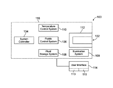
[0047] Figure 1 is a block diagram of an exemplary bioassay system 100 for
biological
or chemical analysis formed in accordance with one embodiment. The term
"bioassay" is
not intended to be limiting as the bioassay system 100 may operate to obtain
any
information or data that relates to at least one of a biological or chemical
substance. In
some embodiments, the bioassay system 100 is a workstation that may be similar
to a
bench-top device or desktop computer. For example, a majority (or all) of the
systems and
components for conducting the designated reactions can be within a common
housing 116.
[0048] In particular embodiments, the bioassay system 100 is a nucleic acid
sequencing
system (or sequencer) configured for various applications, including but not
limited to de
novo sequencing, resequencing of whole genomes or target genomic regions, and
metagenomics. The sequencer may also be used for DNA or RNA analysis. In some
embodiments, the bioassay system 100 may also be configured to generate
reaction sites in
a biosensor. For example, the bioassay system 100 may be configured to receive
a sample
and generate surface attached clusters of clonally amplified nucleic acids
derived from the
sample. Each cluster may constitute or be part of a reaction site in the
biosensor.
[0049] The exemplary bioassay system 100 may include a system receptacle or
interface
112 that is configured to interact with a biosensor 102 to perform designated
reactions
within the biosensor 102. In the following description with respect to Figure
1, the
biosensor 102 is loaded into the system receptacle 112. However, it is
understood that a
cartridge that includes the biosensor 102 may be inserted into the system
receptacle 112
and in some states the cartridge can be removed temporarily or permanently. As
described
above, the cartridge may include, among other things, fluidic control and
fluidic storage
components.
[0050] In particular embodiments, the bioassay system 100 is configured to
perform a
-16-
Date Recue/Date Received 2021-10-07
large number of parallel reactions within the biosensor 102. The biosensor 102
includes
one or more reaction sites where designated reactions can occur. The reaction
sites may
be, for example, immobilized to a solid surface of the biosensor or
immobilized to beads
(or other movable substrates) that are located within corresponding reaction
chambers of
the biosensor. The reaction sites can include, for example, clusters of
clonally amplified
nucleic acids. The biosensor 102 may include a solid-state imaging device
(e.g., CCD or
CMOS imager) and a flow cell mounted thereto. The flow cell may include one or
more
flow channels that receive a solution from the bioassay system 100 and direct
the solution
toward the reaction sites. Optionally, the biosensor 102 can be configured to
engage a
thermal element for transferring thermal energy into or out of the flow
channel.
[0051] The bioassay system 100 may include various components, assemblies, and
systems (or sub-systems) that interact with each other to perform a
predetermined method
or assay protocol for biological or chemical analysis. For example, the
bioassay system
100 includes a system controller 104 that may communicate with the various
components,
assemblies, and sub-systems of the bioassay system 100 and also the biosensor
102. For
example, in addition to the system receptacle 112, the bioassay system 100 may
also
include a fluidic control system 106 to control the flow of fluid throughout a
fluid network
of the bioassay system 100 and the biosensor 102; a fluid storage system 108
that is
configured to hold all fluids (e.g., gas or liquids) that may be used by the
bioassay system;
a temperature control system 110 that may regulate the temperature of the
fluid in the fluid
network, the fluid storage system 108, and/or the biosensor 102; and an
illumination
system 111 that is configured to illuminate the biosensor 102. As described
above, if a
cartridge having the biosensor 102 is loaded into the system receptacle 112,
the cartridge
may also include fluidic control and fluidic storage components.
[0052] Also shown, the bioassay system 100 may include a user interface 114
that
interacts with the user. For example, the user interface 114 may include a
display 113 to
display or request information from a user and a user input device 115 to
receive user
inputs. In some embodiments, the display 113 and the user input device 115 are
the same
device. For example, the user interface 114 may include a touch-sensitive
display
-17-
Date Recue/Date Received 2021-10-07
configured to detect the presence of an individual's touch and also identify a
location of the
touch on the display. However, other user input devices 115 may be used, such
as a
mouse, touchpad, keyboard, keypad, handheld scanner, voice-recognition system,
motion-
recognition system, and the like. As will be discussed in greater detail
below, the bioassay
system 100 may communicate with various components, including the biosensor
102 (e.g.
in the form of a cartridge), to perform the designated reactions. The bioassay
system 100
may also be configured to analyze data obtained from the biosensor to provide
a user with
desired information.
[0053] The system controller 104 may include any processor-based or
microprocessor-
based system, including systems using microcontrollers, reduced instruction
set computers
(RISC), application specific integrated circuits (ASICs), field programmable
gate array
(FPGAs), logic circuits, and any other circuit or processor capable of
executing functions
described herein. The above examples are exemplary only, and are thus not
intended to
limit in any way the definition and/or meaning of the term system controller.
In the
exemplary embodiment, the system controller 104 executes a set of instructions
that are
stored in one or more storage elements, memories, or modules in order to at
least one of
obtain and analyze detection data. Storage elements may be in the form of
information
sources or physical memory elements within the bioassay system 100.
[0054] The set of instructions may include various commands that instruct the
bioassay
system 100 or biosensor 102 to perform specific operations such as the methods
and
processes of the various embodiments described herein. The set of instructions
may be in
the form of a software program, which may form part of a tangible, non-
transitory
computer readable medium or media. As used herein, the terms "software" and
"firmware" are interchangeable, and include any computer program stored in
memory for
execution by a computer, including RAM memory, ROM memory, EPROM memory,
EEPROM memory, and non-volatile RAM (NVRAM) memory. The above memory types
are exemplary only, and are thus not limiting as to the types of memory usable
for storage
of a computer program.
[0055] The software may be in various forms such as system software or
application
-18-
Date Recue/Date Received 2021-10-07
software. Further, the software may be in the form of a collection of separate
programs, or
a program module within a larger program or a portion of a program module. The
software also may include modular programming in the form of object-oriented
programming. After obtaining the detection data, the detection data may be
automatically
processed by the bioassay system 100, processed in response to user inputs, or
processed in
response to a request made by another processing machine (e.g., a remote
request through
a communication link).
[0056] The system controller 104 may be connected to the biosensor 102 and the
other
components of the bioassay system 100 via communication links. The system
controller
104 may also be communicatively connected to off-site systems or servers. The
communication links may be hardwired or wireless. The system controller 104
may
receive user inputs or commands, from the user interface 114 and the user
input device
115.
[0057] The fluidic control system 106 includes a fluid network and is
configured to
direct and regulate the flow of one or more fluids through the fluid network.
The fluid
network may be in fluid communication with the biosensor 102 and the fluid
storage
system 108. For example, select fluids may be drawn from the fluid storage
system 108
and directed to the biosensor 102 in a controlled manner, or the fluids may be
drawn from
the biosensor 102 and directed toward, for example, a waste reservoir in the
fluid storage
system 108. Although not shown, the fluidic control system 106 may include
flow sensors
that detect a flow rate or pressure of the fluids within the fluid network.
The sensors may
communicate with the system controller 104.
[0058] The temperature control system 110 is configured to regulate the
temperature of
fluids at different regions of the fluid network, the fluid storage system
108, and/or the
biosensor 102. For example, the temperature control system 110 may include a
thermocycler that interfaces with the biosensor 102 and controls the
temperature of the
fluid that flows along the reaction sites in the biosensor 102. The
temperature control
system 110 may also regulate the temperature of solid elements or components
of the
bioassay system 100 or the biosensor 102. Although not shown, the temperature
control
-19-
Date Recue/Date Received 2021-10-07
system 110 may include sensors to detect the temperature of the fluid or other
components.
The sensors may communicate with the system controller 104.
[0059] The fluid storage system 108 is in fluid communication with the
biosensor 102
and may store various reaction components or reactants that are used to
conduct the
designated reactions therein. The fluid storage system 108 may also store
fluids for
washing or cleaning the fluid network and biosensor 102 and for diluting the
reactants.
For example, the fluid storage system 108 may include various reservoirs to
store samples,
reagents, enzymes, other biomolecules, buffer solutions, aqueous, and non-
polar solutions,
and the like. Furthermore, the fluid storage system 108 may also include waste
reservoirs
for receiving waste products from the biosensor 102. In embodiments that
include a
cartridge, the cartridge may include one or more of a fluid storage system,
fluidic control
system or temperature control system. Accordingly, one or more of the
components set
forth herein as relating to those systems can be contained within a cartridge
housing. For
example, a cartridge can have various reservoirs to store samples, reagents,
enzymes, other
biomolecules, buffer solutions, aqueous, and non-polar solutions, waste, and
the like. As
such, one or more of a fluid storage system, fluidic control system or
temperature control
system can be removably engaged with a bioassay system via a cartridge or
other
biosensor.
[0060] The illumination system 111 may include a light source (e.g., one or
more LEDs)
and a plurality of optical components to illuminate the biosensor. Examples of
light
sources may include lasers, arc lamps, LEDs, or laser diodes. The optical
components may
be, for example, reflectors, dichroics, beam splitters, collimators, lenses,
filters, wedges,
prisms, minors, detectors, and the like. In embodiments that use an
illumination system,
the illumination system 111 may be configured to direct an excitation light to
reaction
sites. As one example, fluorophores may be excited by green wavelengths of
light, as such
the wavelength of the excitation light may be approximately 532 nm.
[0061] The system receptacle or interface 112 is configured to engage the
biosensor 102
in at least one of a mechanical, electrical, and fluidic manner. The system
receptacle 112
may hold the biosensor 102 in a desired orientation to facilitate the flow of
fluid through
-20-
Date Recue/Date Received 2021-10-07
the biosensor 102. The system receptacle 112 may also include electrical
contacts that are
configured to engage the biosensor 102 so that the bioassay system 100 may
communicate
with the biosensor 102 and/or provide power to the biosensor 102. Furthermore,
the
system receptacle 112 may include fluidic ports (e.g., nozzles) that are
configured to
engage the biosensor 102. In some embodiments, the biosensor 102 is removably
coupled
to the system receptacle 112 in a mechanical manner, in an electrical manner,
and also in a
fluidic manner.
[0062] In addition, the bioassay system 100 may communicate remotely with
other
systems or networks or with other bioassay systems 100. Detection data
obtained by the
bioassay system(s) 100 may be stored in a remote database.
[0063] Figure 2 is a block diagram of the system controller 104 in the
exemplary
embodiment. In one embodiment, the system controller 104 includes one or more
processors or modules that can communicate with one another. Each of the
processors or
modules may include an algorithm (e.g., instructions stored on a tangible
and/or non-
transitory computer readable storage medium) or sub-algorithms to perform
particular
processes. The system controller 104 is illustrated conceptually as a
collection of modules,
but may be implemented utilizing any combination of dedicated hardware boards,
DSPs,
processors, etc. Alternatively, the system controller 104 may be implemented
utilizing an
off-the-shelf PC with a single processor or multiple processors, with the
functional
operations distributed between the processors. As a further option, the
modules described
below may be implemented utilizing a hybrid configuration in which certain
modular
functions are performed utilizing dedicated hardware, while the remaining
modular
functions are performed utilizing an off-the-shelf PC and the like. The
modules also may
be implemented as software modules within a processing unit.
[0064] During operation, a communication link 120 may transmit information
(e.g.
commands) to or receive information (e.g. data) from the biosensor 102 (Figure
1) and/or
the sub-systems 106, 108, 110 (Figure 1). A communication link 122 may receive
user
input from the user interface 114 (Figure 1) and transmit data or information
to the user
interface 114. Data from the biosensor 102 or sub-systems 106, 108, 110 may be
-21-
Date Recue/Date Received 2021-10-07
processed by the system controller 104 in real-time during a bioassay session.
Additionally or alternatively, data may be stored temporarily in a system
memory during a
bioassay session and processed in slower than real-time or off-line operation.
[0065] As shown in Figure 2, the system controller 104 may include a plurality
of
modules 131-139 that communicate with a main control module 130. The main
control
module 130 may communicate with the user interface 114 (Figure 1). Although
the
modules 131-139 are shown as communicating directly with the main control
module 130,
the modules 131-139 may also communicate directly with each other, the user
interface
114, and the biosensor 102. Also, the modules 131-139 may communicate with the
main
control module 130 through the other modules.
[0066] The plurality of modules 131-139 include system modules 131-133, 139
that
communicate with the sub-systems 106, 108, 110, and 111, respectively. The
fluidic
control module 131 may communicate with the fluidic control system 106 to
control the
valves and flow sensors of the fluid network for controlling the flow of one
or more fluids
through the fluid network. The fluid storage module 132 may notify the user
when fluids
are low or when the waste reservoir is at or near capacity. The fluid storage
module 132
may also communicate with the temperature control module 133 so that the
fluids may be
stored at a desired temperature. The illumination module 139 may communicate
with the
illumination system 109 to illuminate the reaction sites at designated times
during a
protocol, such as after the designated reactions (e.g., binding events) have
occurred.
[0067] The plurality of modules 131-139 may also include a device module 134
that
communicates with the biosensor 102 and an identification module 135 that
determines
identification information relating to the biosensor 102. The device module
134 may, for
example, communicate with the system receptacle 112 to confirm that the
biosensor has
established an electrical and fluidic connection with the bioassay system 100.
The
identification module 135 may receive signals that identify the biosensor 102.
The
identification module 135 may use the identity of the biosensor 102 to provide
other
information to the user. For example, the identification module 135 may
determine and
then display a lot number, a date of manufacture, or a protocol that is
recommended to be
-22-
Date Recue/Date Received 2021-10-07
run with the biosensor 102.
[0068] The plurality of modules 131-139 may also include a detection data
analysis
module 138 that receives and analyzes the signal data (e.g., image data) from
the biosensor
102. The signal data may be stored for subsequent analysis or may be
transmitted to the
user interface 114 to display desired information to the user. In some
embodiments, the
signal data may be processed by the solid-state imager (e.g., CMOS image
sensor) before
the detection data analysis module 138 receives the signal data.
[0069] Protocol modules 136 and 137 communicate with the main control module
130
to control the operation of the sub-systems 106, 108, and 110 when conducting
predetermined assay protocols. The protocol modules 136 and 137 may include
sets of
instructions for instructing the bioassay system 100 to perform specific
operations pursuant
to predetermined protocols. As shown, the protocol module may be a sequencing-
by-
synthesis (SBS) module 136 that is configured to issue various commands for
performing
sequencing-by-synthesis processes. In SBS, extension of a nucleic acid primer
along a
nucleic acid template is monitored to determine the sequence of nucleotides in
the
template. The underlying chemical process can be polymerization (e.g. as
catalyzed by a
polymerase enzyme) or ligation (e.g. catalyzed by a ligase enzyme). In a
particular
polymerase-based SBS embodiment, fluorescently labeled nucleotides are added
to a
primer (thereby extending the primer) in a template dependent fashion such
that detection
of the order and type of nucleotides added to the primer can be used to
determine the
sequence of the template. For example, to initiate a first SBS cycle, commands
can be
given to deliver one or more labeled nucleotides, DNA polymerase, etc.,
into/through a
flow cell that houses an array of nucleic acid templates. The nucleic acid
templates may be
located at corresponding reaction sites. Those reaction sites where primer
extension causes
a labeled nucleotide to be incorporated can be detected through an imaging
event. During
an imaging event, the illumination system 111 may provide an excitation light
to the
reaction sites. Optionally, the nucleotides can further include a reversible
termination
property that terminates further primer extension once a nucleotide has been
added to a
primer. For example, a nucleotide analog having a reversible terminator moiety
can be
-23-
Date Recue/Date Received 2021-10-07
added to a primer such that subsequent extension cannot occur until a
deblocking agent is
delivered to remove the moiety. Thus, for embodiments that use reversible
termination a
command can be given to deliver a deblocking reagent to the flow cell (before
or after
detection occurs). One or more commands can be given to effect wash(es)
between the
various delivery steps. The cycle can then be repeated n times to extend the
primer by n
nucleotides, thereby detecting a sequence of length n. Exemplary sequencing
techniques
are described, for example, in Bentley et al., Nature 456:53-59 (2008), WO
04/018497; US
7,057,026; WO 91/06678; WO 07/123744; US 7,329,492; US 7,211,414; US
7,315,019;
US 7,405,281, and US 2008/0108082.
[0070] For the nucleotide delivery step of an SBS cycle, either a single type
of
nucleotide can be delivered at a time, or multiple different nucleotide types
(e.g. A, C, T
and G together) can be delivered. For a nucleotide delivery configuration
where only a
single type of nucleotide is present at a time, the different nucleotides need
not have
distinct labels since they can be distinguished based on temporal separation
inherent in the
individualized delivery. Accordingly, a sequencing method or apparatus can use
single
color detection. For example, an excitation source need only provide
excitation at a single
wavelength or in a single range of wavelengths. For a nucleotide delivery
configuration
where delivery results in multiple different nucleotides being present in the
flow cell at one
time, sites that incorporate different nucleotide types can be distinguished
based on
different fluorescent labels that are attached to respective nucleotide types
in the mixture.
For example, four different nucleotides can be used, each having one of four
different
fluorophores. In one embodiment, the four different fluorophores can be
distinguished
using excitation in four different regions of the spectrum. For example, four
different
excitation radiation sources can be used. Alternatively, fewer than four
different excitation
sources can be used, but optical filtration of the excitation radiation from a
single source
can be used to produce different ranges of excitation radiation at the flow
cell.
[0071] In some embodiments, fewer than four different colors can be detected
in a
mixture having four different nucleotides. For example, pairs of nucleotides
can be
detected at the same wavelength, but distinguished based on a difference in
intensity for
-24-
Date Recue/Date Received 2021-10-07
one member of the pair compared to the other, or based on a change to one
member of the
pair (e.g. via chemical modification, photochemical modification or physical
modification)
that causes apparent signal to appear or disappear compared to the signal
detected for the
other member of the pair. Exemplary apparatus and methods for distinguishing
four
different nucleotides using detection of fewer than four colors are described
for example in
US Pat. App. Ser. Nos. 61/538,294 and 61/619,878. Also of interest is U.S.
Application
No. 13/624,200, which was filed on September 21, 2012.
[0072] The plurality of protocol modules may also include a sample-preparation
(or
generation) module 137 that is configured to issue commands to the fluidic
control system
106 and the temperature control system 110 for amplifying a product within the
biosensor
102. For example, the biosensor 102 may be engaged to the bioassay system 100.
The
amplification module 137 may issue instructions to the fluidic control system
106 to
deliver necessary amplification components to reaction chambers within the
biosensor 102.
In other embodiments, the reaction sites may already contain some components
for
amplification, such as the template DNA and/or primers. After delivering the
amplification components to the reaction chambers, the amplification module
137 may
instruct the temperature control system 110 to cycle through different
temperature stages
according to known amplification protocols. In some embodiments, the
amplification
and/or nucleotide incorporation is performed isothermally.
[0073] The SBS module 136 may issue commands to perform bridge PCR where
clusters of clonal amplicons are formed on localized areas within a channel of
a flow cell.
After generating the amplicons through bridge PCR, the amplicons may be
"linearized" to
make single stranded template DNA, or sstDNA, and a sequencing primer may be
hybridized to a universal sequence that flanks a region of interest. For
example, a
reversible terminator-based sequencing by synthesis method can be used as set
forth above
or as follows.
[0074] Each sequencing cycle can extend a sstDNA by a single base which can be
accomplished for example by using a modified DNA polymerase and a mixture of
four
types of nucleotides. The different types of nucleotides can have unique
fluorescent labels,
-25-
Date Recue/Date Received 2021-10-07
and each nucleotide can further have a reversible terminator that allows only
a single-base
incorporation to occur in each cycle. After a single base is added to the
sstDNA, excitation
light may be incident upon the reaction sites and fluorescent emissions may be
detected.
After detection, the fluorescent label and the terminator may be chemically
cleaved from
the sstDNA. Another similar sequencing cycle may follow. In such a sequencing
protocol, the SBS module 136 may instruct the fluidic control system 106 to
direct a flow
of reagent and enzyme solutions through the biosensor 102. Exemplary
reversible
terminator-based SBS methods which can be utilized with the apparatus and
methods set
forth herein are described in US Patent Application Publication No.
2007/0166705 Al, US
Patent Application Publication No. 2006/0188901 Al, US Patent No. 7,057,026,
US Patent
Application Publication No. 2006/0240439 Al, US Patent Application Publication
No.
2006/0281109 Al, PCT Publication No. WO 05/065814, US Patent Application
Publication No. 2005/0100900 Al, PCT Publication No. WO 06/064199 and PCT
Publication No. WO 07/010251. Exemplary reagents for reversible terminator-
based SBS
are described in US 7,541,444; US 7,057,026; US 7,414,116; US 7,427,673; US
7,566,537; US 7,592,435 and WO 07/135368.
[0075] In some embodiments, the amplification and SBS modules may operate in a
single assay protocol where, for example, template nucleic acid is amplified
and
subsequently sequenced within the same cartridge.
[0076] The bioassay system 100 may also allow the user to reconfigure an assay
protocol. For example, the bioassay system 100 may offer options to the user
through the
user interface 114 for modifying the determined protocol. For example, if it
is determined
that the biosensor 102 is to be used for amplification, the bioassay system
100 may request
a temperature for the annealing cycle. Furthermore, the bioassay system 100
may issue
warnings to a user if a user has provided user inputs that are generally not
acceptable for
the selected assay protocol.
[0077] Figure 3 is a block diagram of an exemplary workstation 200 for
biological or
chemical analysis in accordance with one embodiment. The workstation 200 may
have
similar features, systems, and assemblies as the bioassay system 100 described
above. For
-26-
Date Recue/Date Received 2021-10-07
example, the workstation 200 may have a fluidic control system, such as the
fluidic control
system 106 (Figure 1), that is fluidicly coupled to a biosensor (or cartridge)
235 through a
fluid network 238. The fluid network 238 may include a reagent cartridge 240,
a valve
block 242, a main pump 244, a debubbler 246, a 3-way valve 248, a flow
restrictor 250, a
waste removal system 252, and a purge pump 254. In particular embodiments,
most of the
components or all of the components described above are within a common
workstation
housing (not shown). Although not shown, the workstation 200 may also include
an
illumination system, such as the illumination system 111, that is configured
to provide an
excitation light to the reaction sites.
[0078] A flow of fluid is indicated by arrows along the fluid network 238. For
example,
reagent solutions may be removed from the reagent cartridge 240 and flow
through the
valve block 242. The valve block 242 may facilitate creating a zero-dead
volume of the
fluid flowing to the cartridge 235 from the reagent cartridge 240. The valve
block 242 can
select or permit one or more liquids within the reagent cartridge 240 to flow
through the
fluid network 238. For example, the valve block 242 can include solenoid
valves that have
a compact arrangement. Each solenoid valve can control the flow of a fluid
from a single
reservoir bag. In some embodiments, the valve block 242 can permit two or more
different
liquids to flow into the fluid network 238 at the same time thereby mixing the
two or more
different liquids. After leaving the valve block 242, the fluid may flow
through the main
pump 244 and to the debubbler 246. The debubbler 246 is configured to remove
unwanted
gases that have entered or been generated within the fluid network 238.
[0079] From the debubbler 246, fluid may flow to the 3-way valve 248 where the
fluid
is either directed to the cartridge 235 or bypassed to the waste removal
system 252. A
flow of the fluid within the cartridge 235 may be at least partially
controlled by the flow
restrictor 250 located downstream from the cartridge 235. Furthermore, the
flow restrictor
250 and the main pump 244 may coordinate with each other to control the flow
of fluid
across reaction sites and/or control the pressure within the fluid network
238. Fluid may
flow through the cartridge 235 and onto the waste removal system 252.
Optionally, fluid
-27-
Date Recue/Date Received 2021-10-07
may flow through the purge pump 254 and into, for example, a waste reservoir
bag within
the reagent cartridge 240.
[0080] Also shown in Figure 3, the workstation 200 may include a temperature
control
system, such as the temperature control system 110, that is configured to
regulate or
control a thermal environment of the different components and sub-systems of
the
workstation 200. The temperature control system 110 can include a reagent
cooler 264
that is configured to control the temperature requirements of various fluids
used by the
workstation 200, and a thermocycler 266 that is configured to control the
temperature of a
cartridge 235. The thermocycler 266 can include a thermal element (not shown)
that
interfaces with the cartridge.
[0081] Furthermore, the workstation 200 may include a system controller or SBS
board
260 that may have similar features as the system controller 104 described
above. The SBS
board 260 may communicate with the various components and sub-systems of the
workstation 200 as well as the cartridge 235. Furthermore, the SBS board 260
may
communicate with remote systems to, for example, store data or receive
commands from
the remote systems. The workstation 200 may also include a touch screen user
interface
262 that is operatively coupled to the SBS board 260 through a single-board
computer
(SBC) 272. The workstation 200 may also include one or more user accessible
data
communication ports and/or drives. For example a workstation 200 may include
one or
more universal serial bus (USB) connections for computer peripherals, such as
a flash or
jump drive, a compact-flash (CF) drive and/or a hard drive 270 for storing
user data in
addition to other software.
[0082] Figure 4 is a perspective view of a workstation 300 and a cartridge 302
that may
include one or more biosensors (not shown) as described herein. The
workstation 300 may
include similar components as described above with respect to the bioassay
system 100
and the workstation 200 and may operate in a similar manner. For example, the
workstation 300 may include a workstation housing 304 and a system receptacle
306 that
is configured to receive and engage the cartridge 302. The system receptacle
may at least
one of fluidically or electrically engage the cartridge 302. The workstation
housing 304
-28-
Date Recue/Date Received 2021-10-07
may hold, for example, a system controller, a fluid storage system, a fluidic
control system,
and a temperature control system as described above. In Figure 4, the
workstation 300
does not include a user interface or display that is coupled to the
workstation housing 304.
However, a user interface may be communicatively coupled to the housing 304
(and the
components/systems therein) through a communication link. Thus, the user
interface and
the workstation 300 may be remotely located with respect to each other.
Together, the user
interface and the workstation 300 (or a plurality of workstations) may
constitute a bioassay
system.
[0083] As shown, the cartridge 302 includes a cartridge housing 308 having at
least one
port 310 that provides access to an interior of the cartridge housing 308. For
example, a
solution that is configured to be used in the cartridge 302 during the
controlled reactions
may be inserted through the port 310 by a technician or by the workstation
300. The
system receptacle 306 and the cartridge 302 may be sized and shaped relative
to each other
such that the cartridge 302 may be inserted into a receptacle cavity (not
shown) of the
system receptacle 306.
[0084] Figure 5 is a front view of a rack assembly 312 having a cabinet or
carriage 314
with a plurality of the workstations 300 loaded thereon. The cabinet 314 may
include one
or more shelves 316 that define one or more reception spaces 318 configured to
receive
one or more workstations 300. Although not shown, the workstations 300 may be
communicatively coupled to a communication network that permits a user to
control
operation of the workstations 300. In some embodiments, a bioassay system
includes a
plurality of workstations, such as the workstations 300, and a single user
interface
configured to control operation of the multiple workstations.
[0085] Figure 6 illustrates various features of the cartridge 302 (Figure 4)
in accordance
with one embodiment. As shown, the cartridge 302 may include a sample assembly
320,
and the system receptacle 306 may include a light assembly 322. Stage 346
shown in
Figure 6 represents the spatial relationship between the first and second sub-
assemblies
320 and 322 when they are separate from each other. At stage 348, the first
and second
-29-
Date Recue/Date Received 2021-10-07
sub-assemblies 320 and 322 are joined together. The cartridge housing 308
(Figure 4) may
enclose the joined first and second sub-assemblies 320 and 322.
[0086] In the illustrated embodiment, the first sub-assembly 320 includes a
base 326 and
a reaction-component body 324 that is mounted onto the base 326. Although not
shown,
one or more biosensors may be mounted to the base 326 in a recess 328 that is
defined, at
least in part, by the reaction-component body 324 and the base 326. For
example, at least
four biosensors may be mounted to the base 326. In some embodiments, the base
326 is a
printed circuit board having circuitry that enables communication between the
different
components of the cartridge and the workstation 300 (Figure 4). For example,
the
reaction-component body 324 may include a rotary valve 330 and reagent
reservoirs 332
that are fluidically coupled to the rotary valve 330. The reaction-component
body 324 may
also include additional reservoirs 334.
[0087] The second sub-assembly 322 includes a light assembly 336 that includes
a
plurality of light directing channels 338. Each light directing channel 338 is
optically
coupled to a light source (not shown), such as a light-emitting diode (LED).
The light
source(s) are configured to provide an excitation light that is directed by
the light directing
channels 338 onto the biosensors. In alternative embodiments, the cartridge
may not
include a light source(s). In such embodiments, the light source(s) may be
located in the
workstation 300. When the cartridge is inserted into the system receptacle 306
(Figure 4),
the cartridge 302 may align with the light source(s) so that the biosensors
may be
illuminated.
[0088] Also shown in Figure 6, the second sub-assembly 322 includes a
cartridge pump
340 that is fluidically coupled to ports 342 and 344. When the first and
second sub-
assemblies 320 and 322 are joined together, the port 342 is coupled to the
rotary valve 330
and the port 344 is coupled to the other reservoirs 334. The cartridge pump
340 may be
activated to direct reaction components from the reservoirs 332 and/or 334 to
the
biosensors according to a designated protocol.
[0089] Figure 7 illustrates a cross-section of a portion of an exemplary
biosensor 400
formed in accordance with one embodiment. The biosensor 400 may include
similar
-30-
Date Recue/Date Received 2021-10-07
features as the biosensor 102 (Figure 1) described above and may be used in,
for example,
the cartridge 302 (Figure 4). As shown, the biosensor 400 may include a flow
cell 402 that
is coupled directly or indirectly to a detection device 404. The flow cell 402
may be
mounted to the detection device 404. In the illustrated embodiment, the flow
cell 402 is
affixed directly to the detection device 404 through one or more securing
mechanisms
(e.g., adhesive, bond, fasteners, and the like). In some embodiments, the flow
cell 402
may be removably coupled to the detection device 404.
[0090] In the illustrated embodiment, the detection device 404 includes a
device base
425. In particular embodiments, the device base 425 includes a plurality of
stacked layers
(e.g., silicon layer, dielectric layer, metal-dielectric layers, etc.). The
device base 425 may
include a sensor array 424 of light sensors 440, a guide array 426 of light
guides 462, and a
reaction array 428 of reaction recesses 408 that have corresponding reaction
sites 414. In
certain embodiments, the components are arranged such that each light sensor
440 aligns
with a single light guide 462 and a single reaction site 414. However, in
other
embodiments, a single light sensor 440 may receive photons through more than
one light
guide 462 and/or from more than one reaction site 414. As used herein, a
single light
sensor may include one pixel or more than one pixel.
[0091] Moreover, it is noted that the term "array" or "sub-array" does not
necessarily
include each and every item of a certain type that the detection device may
have. For
example, the sensor array 424 may not include each and every light sensor in
the detection
device 404. Instead, the detection device 404 may include other light sensors
(e.g., other
array(s) of light sensors). As another example, the guide array 426 may not
include each
and every light guide of the detection device. Instead, there may be other
light guides that
are configured differently than the light guides 462 or that have different
relationships with
other elements of the detection device 404. As such, unless explicitly recited
otherwise,
the term "array" may or may not include all such items of the detection
device.
[0092] In the illustrated embodiment, the flow cell 402 includes a sidewall
406 and a
flow cover 410 that is supported by the sidewall 406 and other sidewalls (not
shown). The
sidewalls are coupled to the detector surface 412 and extend between the flow
cover 410
-31 -
Date Recue/Date Received 2021-10-07
and the detector surface 412. In some embodiments, the sidewalls are formed
from a
curable adhesive layer that bonds the flow cover 410 to the detection device
404.
[0093] The flow cell 402 is sized and shaped so that a flow channel 418 exists
between
the flow cover 410 and the detection device 404. As shown, the flow channel
418 may
include a height Hi. By way of example only, the height Hi may be between
about 50-400
[tm (microns) or, more particularly, about 80-200 [tm. In the illustrated
embodiment, the
height Hi is about 100 [tm. The flow cover 410 may include a material that is
transparent
to excitation light 401 propagating from an exterior of the biosensor 400 into
the flow
channel 418. As shown in Figure 7, the excitation light 401 approaches the
flow cover 410
at a non-orthogonal angle. However, this is only for illustrative purposes as
the excitation
light 401 may approach the flow cover 410 from different angles.
[0094] Also shown, the flow cover 410 may include inlet and outlet ports 420,
422 that
are configured to fluidically engage other ports (not shown). For example, the
other ports
may be from the cartridge 302 (Figure 4) or the workstation 300 (Figure 4).
The flow
channel 418 is sized and shaped to direct a fluid along the detector surface
412. The height
Hi and other dimensions of the flow channel 418 may be configured to maintain
a
substantially even flow of a fluid along the detector surface 412. The
dimensions of the
flow channel 418 may also be configured to control bubble formation.
[0095] The sidewalls 406 and the flow cover 410 may be separate components
that are
coupled to each other. In other embodiments, the sidewalls 406 and the flow
cover 410
may be integrally formed such that the sidewalls 406 and the flow cover 410
are formed
from a continuous piece of material. By way of example, the flow cover 410 (or
the flow
cell 402) may comprise a transparent material, such as glass or plastic. The
flow cover 410
may constitute a substantially rectangular block having a planar exterior
surface and a
planar inner surface that defines the flow channel 418. The block may be
mounted onto
the sidewalls 406. Alternatively, the flow cell 402 may be etched to define
the flow cover
410 and the sidewalls 406. For example, a recess may be etched into the
transparent
material. When the etched material is mounted to the detection device 404, the
recess may
become the flow channel 418.
-32-
Date Recue/Date Received 2021-10-07
[0096] The detection device 404 has a detector surface 412 that may be
functionalized
(e.g., chemically or physically modified in a suitable manner for conducting
designated
reactions). For example, the detector surface 412 may be functionalized and
may include a
plurality of reaction sites 414 having one or more biomolecules immobilized
thereto. The
detector surface 412 has an array of reaction recesses or open-sided reaction
chambers 408.
Each of the reaction recesses 408 may include one or more of the reaction
sites 414. The
reaction recesses 408 may be defined by, for example, an indent or change in
depth along
the detector surface 412. In other embodiments, the detector surface 412 may
be
substantially planar.
[0097] As shown in Figure 7, the reaction sites 414 may be distributed in a
pattern along
the detector surface 412. For instance, the reactions sites 414 may be located
in rows and
columns along the detector surface 412 in a manner that is similar to a
microarray.
However, it is understood that various patterns of reaction sites may be used.
The reaction
sites may include biological or chemical substances that emit light signals.
For example,
the biological or chemical substances of the reactions sites may generate
light emissions in
response to the excitation light 401. In particular embodiments, the reaction
sites 414
include clusters or colonies of biomolecules (e.g., oligonucleotides) that are
immobilized
on the detector surface 412.
[0098] Figure 8 is an enlarged cross-section of the detection device 404
showing various
features in greater detail. More specifically, Figure 8 shows a single light
sensor 440, a
single light guide 462 for directing light emissions toward the light sensor
440, and
associated circuitry 446 for transmitting signals based on the light emissions
(e.g., photons)
detected by the light sensor 440. It is understood that the other light
sensors 440 of the
sensor array 424 (Figure 7) and associated components may be configured in an
identical
or similar manner. It is also understood, however, the detection device 404 is
not required
to be manufactured identically or uniformly throughout. Instead, one or more
light sensors
440 and/or associated components may be manufactured differently or have
different
relationships with respect to one another.
-33-
Date Recue/Date Received 2021-10-07
[0099] The circuitry 446 may include interconnected conductive elements (e.g.,
conductors, traces, vias, interconnects, etc.) that are capable of conducting
electrical
current, such as the transmission of data signals that are based on detected
photons. For
example, in some embodiments, the circuitry 446 may be similar to or include a
microcircuit arrangement, such as the microcircuit arrangement described in
U.S. Patent
No. 7,595,883. The detection device 404 and/or the device base 425 may
comprise an
integrated circuit having a planar array of the light sensors 440. The
circuitry 446 formed
within the detection device 425 may be configured for at least one of signal
amplification,
digitization, storage, and processing. The circuitry may collect and analyze
the detected
light emissions and generate data signals for communicating detection data to
a bioassay
system. The circuitry 446 may also perform additional analog and/or digital
signal
processing in the detection device 404.
[00100] The device base 425 may be manufactured using integrated circuit
manufacturing processes, such as processes used to manufacture complementary-
metal-
oxide semiconductors (CMOSs). For example, the device base 425 may include a
plurality
of stacked layers 431-437 including a sensor layer or base 431, which is a
silicon layer or
wafer in the illustrated embodiment. The sensor layer 431 may include the
light sensor
440 and gates 441-443 that are formed with the sensor layer 431. The gates 441-
443 are
electrically coupled to the light sensor 440. When the detection device 404 is
fully formed
as shown in Figures 7 and 8, the light sensor 440 may be electrically coupled
to the
circuitry 446 through the gates 441-443.
[00101] As used herein, the term "layer" is not limited to a single continuous
body of
material unless otherwise noted. For example, the sensor layer 431 may include
multiple
sub-layers that are different materials and/or may include coatings,
adhesives, and the like.
Furthermore, one or more of the layers (or sub-layers) may be modified (e.g.,
etched,
deposited with material, etc.) to provide the features described herein.
[00102] In some embodiments, each light sensor 440 has a detection area that
is less
than about 50 [tm2. In particular embodiments, the detection area is less than
about 10
[tm2. In more particular embodiments, the detection area is about 2 [tm2. In
such cases, the
-34-
Date Recue/Date Received 2021-10-07
light sensor 440 may constitute a single pixel. An average read noise of each
pixel in a
light sensor 440 may be, for example, less than about 150 electrons. In more
particular
embodiments, the read noise may be less than about 5 electrons. The resolution
of the
array of light sensors 440 may be greater than about 0.5 megapixels (Mpixels).
In more
specific embodiments, the resolution may be greater than about 5 Mpixels and,
more
particularly, greater than about 10 Mpixels.
[00103] The device layers also include a plurality of metal-dielectric layers
432-437,
which are hereinafter referred to as substrate layers. In the illustrated
embodiment, each of
the substrate layers 432-437 includes metallic elements (e.g., W (tungsten),
Cu (copper), or
Al (aluminum)) and dielectric material (e.g., SiO2). Various metallic elements
and
dielectric material may be used, such as those suitable for integrated circuit
manufacturing.
However, in other embodiments, one or more of the substrate layers 432-437 may
include
only dielectric material, such as one or more layers of SiO2.
[00104] With respect to the specific embodiment shown in Figure 8, the first
substrate
layer 432 may include metallic elements referred to as M1 that are embedded
within
dielectric material (e.g., SiO2). The metallic elements M1 comprise, for
example, W
(tungsten). The metallic elements M1 extend entirely through the substrate
layer 432 in
the illustrated embodiment. The second substrate layer 433 includes metallic
elements M2
and dielectric material as well as a metallic interconnects (M2/M3). The third
substrate
layer 434 includes metallic elements M3 and metal interconnects (M3/M4). The
fourth
substrate layer 435 also includes metallic elements M4. The device base 425
also includes
fifth and sixth substrate layers 436, 437, which are described in greater
detail below.
[00105] As shown, the metallic elements and interconnects are connected to
each other
to form at least a portion of the circuitry 446. In the illustrated
embodiment, the metallic
elements Ml, M2, M3, M4 include W (tungsten), Cu (copper), and/or aluminum
(Al) and
the metal interconnects M2/M3 and M3/M4 include W (tungsten), but it is
understood that
other materials and configurations may be used. It is also noted that the
device base 425
and the detection device 404 shown in Figures 7 and 8 are for illustrative
purposes only.
-35-
Date Recue/Date Received 2021-10-07
For example, other embodiments may include fewer or additional layers than
those shown
in Figures 7 and 8 and/or different configurations of metallic elements.
[00106] In some embodiments, the detection device 404 includes a shield layer
450 that
extends along an outer surface 464 of the device base 425. In the illustrated
embodiment,
the shield layer 450 is deposited directly along the outer surface 464 of the
substrate layer
437. However, an intervening layer may be disposed between the substrate layer
437 and
the shield layer 450 in other embodiments. The shield layer 450 may include a
material
that is configured to block, reflect, and/or significantly attenuate the light
signals that are
propagating from the flow channel 418. The light signals may be the excitation
light 401
and/or the light emissions 466 (shown in Figure 9). By way of example only,
the shield
layer 450 may comprise tungsten (W).
[00107] As shown in Figure 8, the shield layer 450 includes an aperture or
opening 452
therethrough. The shield layer 450 may include an array of such apertures 452.
In some
embodiments, the shield layer 450 may extend continuously between adjacent
apertures
452. As such, the light signals from the flow channel 418 may be blocked,
reflected,
and/or significantly attenuated to prevent detection of such light signals by
the light
sensors 440. However, in other embodiments, the shield layer 450 does not
extend
continuously between the adjacent apertures 452 such then one or more openings
other
than the apertures 452 exits in the shield layer 450.
[00108] The detection device 404 may also include a passivation layer 454 that
extends
along the shield layer 450 and across the apertures 452. The shield layer 450
may extend
over the apertures 452 thereby directly or indirectly covering the apertures
452. The shield
layer 450 may be located between the passivation layer 454 and the device base
425. An
adhesive or promoter layer 458 may be located therebetween to facilitate
coupling the
passivation and shield layers 454, 450. The passivation layer 454 may be
configured to
protect the device base 425 and the shield layer 450 from the fluidic
environment of the
flow channel 418.
[00109] In some cases, the passivation layer 454 may also be configured to
provide a
solid surface (i.e., the detector surface 412) that permits biomolecules or
other analytes-of-
-36-
Date Recue/Date Received 2021-10-07
interest to be immobilized thereon. For example, each of the reaction sites
414 may
include a cluster of biomolecules that are immobilized to the detector surface
412 of the
passivation layer 454. Thus, the passivation layer 454 may be formed from a
material that
permits the reaction sites 414 to be immobilized thereto. The passivation
layer 454 may
also comprise a material that is at least transparent to a desired fluorescent
light. By way
of example, the passivation layer 454 may include silicon nitride (Si3N4)
and/or silica
(SiO2). However, other suitable material(s) may be used. In addition, the
passivation layer
454 may be physically or chemically modified to facilitate immobilizing the
biomolecules
and/or to facilitate detection of the light emissions.
[00110] In the illustrated embodiment, a portion of the passivation layer 454
extends
along the shield layer 450 and a portion of the passivation layer 454 extends
directly along
filter material 460 of a light guide 462. The reaction recess 408 may be
formed directly
over the light guide 462. In some cases, prior to the passivation layer 454
being deposited
along the shield layer 450 or adhesion layer 458, a base hole or cavity 456
may be formed
within the device base 425. For example, the device base 425 may be etched to
form an
array of the base holes 456. In particular embodiments, the base hole 456 is
an elongated
space that extends from proximate the aperture 452 toward the light sensor
440. The base
hole may extend lengthwise along a central longitudinal axis 468. A three-
dimensional
shape of the base hole 456 may be substantially cylindrical or frustro-conical
in some
embodiments such that a cross-section taken along a plane that extends into
the page of
Figure 8 is substantially circular. The longitudinal axis 468 may extend
through a
geometric center of the cross-section. However, other geometries may be used
in
alternative embodiments. For example, the cross-section may be substantially
square-
shaped or octagonal.
[00111] The filter material 460 may be deposited within the base hole 456
after the base
hole 456 is formed. The filter material 460 may form (e.g., after curing) a
light guide 462.
The light guide 462 is configured to filter the excitation light 401 and
permit the light
emissions 466 to propagate therethrough toward the corresponding light sensor
440. The
light guide 462 may be, for example, an organic absorption filter. By way of
specific
-37-
Date Recue/Date Received 2021-10-07
example only, the excitation light may be about 532 nm and the light emissions
may be
about 570 nm or more.
[00112] In some cases, the organic filter material may be incompatible with
other
materials of the biosensor. For example, organic filter material may have a
coefficient of
thermal expansion that causes the filter material to significantly expand.
Alternatively or
in addition to, the filter material may be unable to sufficiently adhere to
certain layers, such
as the shield layer (or other metal layers). Expansion of the filter material
may cause
mechanical stress on the layers that are adjacent to the filter material or
structurally
connected to the filter material. In some cases, the expansion may cause
cracks or other
unwanted features in the structure of the biosensor. As such, embodiments set
forth herein
may limit the degree to which the filter material expands and/or the degree to
which the
filter material is in contact with other layers. For example, the filter
material of different
light guides may be isolated from each other by the passivation layer. In such
embodiments, the filter material may not contact the metal layer(s). Moreover,
the
passivation layer may resist expansion and/or permit some expansion while
reducing
generation of unwanted structural features (e.g., cracks).
[00113] The light guide 462 may be configured relative to surrounding material
of the
device base 425 (e.g., the dielectric material) to form a light-guiding
structure. For
example, the light guide 462 may have a refractive index of about 2.0 so that
the light
emissions are substantially reflected at an interface between the light guide
462 and the
material of the device base 425. In certain embodiments, the light guide 462
is configured
such that the optical density (OD) or absorbance of the excitation light is at
least about 4
OD. More specifically, the filter material may be selected and the light guide
462 may be
dimensioned to achieve at least 4 OD. In more particular embodiments, the
light guide 462
may be configured to achieve at least about 5 OD or at least about 6 OD. Other
features of
the biosensor 400 may be configured to reduce electrical and optical
crosstalk.
[00114] Figure 9 illustrates an enlarged view of the detector surface 412 and
portions of
the detection device 404 (Figure 7) that are located proximate to the detector
surface 412.
More specifically, the passivation layer 454, the adhesion layer 458, the
shield layer 450,
-38-
Date Recue/Date Received 2021-10-07
and the light guide 462 are shown in Figure 9. Each of the layers may have a
outer (top)
surface or an inner (bottom) surface and may extend along an adjacent layer at
an interface.
In some embodiments, the detector surface 412 is configured to form the
reaction recess
408 proximate to the aperture 452. The reaction recess 408 may be, for
example, an
indent, pit, well, groove, or open-sided chamber or channel. Alternatively,
the detector
surface 412 may be planar without the recesses shown in Figures 7-9. As shown,
the
aperture 452 is defined by an aperture or layer edge 504. The layer edge 504
faces radially
inward toward the longitudinal axis 468.
[00115] The detector surface 412 may include an elevated portion 502 and the
reaction
recess 408 may include a base surface 490. The base surface 490 may extend
substantially
parallel to the shield layer 450. The detector surface 412 may also include a
side surface
492 that extends substantially orthogonal to the base surface 490 and the
elevated portion
502 of the detector surface 412. The side surface 492 may define a periphery
of the
reaction recess 408. Although the elevated portion 502, the base surface 490,
and the side
surface 492 are referenced as separate surfaces it is understood that the
surfaces may be
portions of the detector surface 412. Moreover, it is understood that, due to
manufacturing
tolerances, the surfaces may not have be readily distinct. For example, in
other
embodiments, the base surface 490 and the side surface 492 may be
substantially a single
surface with a concave shape.
[00116] The base surface 490 may represent (or include a point that
represents) a
deepest portion of the passivation layer 454 along the detector surface 412
within the
reaction recess 408. For example, the elevated portion 502 may extend along a
surface
plane Pi and the base surface 490 may extend along a surface plane P2. As
shown, the
surface planes Pi and P2 are offset with respect to each other by a depth or
distance Di.
The surface plane P2 is closer to the light guide 462 or the light sensor 440
(Figure 7) than
the surface plane Pi. In the illustrated embodiment, the depth Di of the base
surface 490 is
substantially continuous due to the base surface 490 being substantially
planar. In other
embodiment, however, the depth Di may vary. For example, the base surface 490
may
-39-
Date Recue/Date Received 2021-10-07
have a concave shape with the depth increasing as the base surface 490 extends
toward a
center or middle thereof.
[00117] The reaction recess 408 may extend toward or be located within the
aperture
452. For instance, at least a portion of the base surface 490 may reside
within the aperture
452. The shield layer 450 may have an outer surface 506 that faces the
passivation layer
454 and an inner surface 508 that faces the device base 425. The outer surface
506 may
extend along a surface plane P3, and the inner surface 508 may extend along a
surface
plane P4. The distance between the surface planes P3 and P4 may represent a
thickness of
the shield layer 450. As shown, the surface plane P3 may be located between
the surface
planes Pi, Pz. As such, the base surface 490 extends within the aperture 452
as defined by
the layer edge 504. In other embodiments, however, the surface plane P2 may be
located
above the surface plane P3 such that the base surface 490 does not reside
within the
aperture 452. Moreover, in some embodiments, the surface plane P2 may be
located below
the surface plane P4 such that base surface 490 is located below the aperture
452.
[00118] The passivation layer 454 includes the detector surface 412 and an
inner surface
510 that extends along the outer surface 506 of the shield layer 450 at an
interface 512. In
some embodiments, the adhesion layer 458 may extend along and define the
interface 512
between the shield layer 450 and the passivation layer 454.
[00119] In the illustrated embodiment, the passivation layer 454 extends
directly along
the light guide 462. More specifically, the inner surface 510 of the
passivation layer 454
may directly engage a material surface 514 of the light guide 462. As used
herein, the
phrase "directly engage" and the like may include the two layers directly
contacting each
other or the two layers being bonded to each other through the use of an
adhesion promoter
material(s). The light guide 462 has an input region 472 that includes the
material surface
514. The input region 472 may represent a portion of the light guide 462 that
initially
receives the light emissions.
[00120] The inner surface 510 may directly engage the material surface 514 at
an
interface 516. The interface 516 may represent a material level of the filter
material 460
that is deposited within the guide cavity 456 (Figure 7). In the illustrated
embodiment, the
-40-
Date Recue/Date Received 2021-10-07
interface 516 is substantially planar such that the interface 516 extends
along an interface
plane P5. The interface plane P5 may extend substantially parallel to one or
more of the
surface planes Pi, P2, P3, P4. In other embodiments, however, the interface
516 may have a
concave shape such that the interface 516 bows toward the light sensor 440
(Figure 8) or in
an opposite direction away from the light sensor 440.
[00121] The passivation layer 454 may fill a void generated when the aperture
452 is
formed. Thus, in some embodiments, the passivation layer 454 may be located
within or
reside in the aperture 452. In particular embodiments, the interface 516 may
be located a
depth D2 into the device base 425. In particular embodiments, the depth D2 may
be
configured such that the interface 516 is located below the aperture 452 as
shown in Figure
8. In such embodiments, the passivation layer 454 may isolate (e.g., separate)
the filter
material 460 and the shield layer 450. Such embodiments may be suitable when
the filter
material 460 and the shield layer 450 are incompatible such that cracks or
other unwanted
features may develop during manufacture of usage of the biosensor 400 (Figure
7). In
other embodiments, at least a portion of the interface 516 may be located
within the
aperture 452.
[00122] Also shown in Figure 9, the passivation layer 454 may form a joint or
corner
region 519. The joint region 519 may include the side surface 492 and extend
around the
longitudinal axis 468. The joint region 519 may include a relatively thicker
portion of the
passivation layer 454 that extends from the elevated portion 502 to the inner
surface 510 at
the material interface 516 (or between the surface plane Pi and the interface
plane Ps). The
dimensions of the joint region 519 may resist mechanical stresses caused by
expansion of
the filter material 460 during manufacture of the biosensor 400 and/or during
thermal
cycling that may occur during designated protocols (e.g., SBS sequencing). As
shown, the
thickness between the surface plane Pi and the interface plane P5 is more than
twice the
thickness between the elevated portion 502 of the detector surface 412 and the
interface
512.
[00123] The reaction site 414 may include biological or chemical substances,
which are
generally represented as dots 520 in Figure 9. The biological or chemical
substances may
-41-
Date Recue/Date Received 2021-10-07
be immobilized to the detector surface 412 or, more specifically, the base and
side surfaces
490, 492. In particular embodiments, the reaction site 414 is located
proximate to the
aperture 452 so that light emissions propagate through the passivation layer
454, through
the aperture 452, and into the input region 472 of the light guide 462.
[00124] In some embodiments, the reaction sites 414 or the biological or
chemical
substances 520 therein may be patterned such that the reaction sites 414 or
substances 520
have predetermined locations. For example, after the passivation layer 454 is
applied, the
reaction sites 414 or portions thereof may be patterned onto the passivation
layer 454. In
the illustrate embodiment, each aperture 452 is associated with a single
reaction site 414
such that the light emissions from the reaction site 414 are directed toward
the
corresponding light sensor 440. The biological or chemical substances 520 in a
single
reaction site 414 may be similar or identical (e.g., a colony of
oligonucleotides that have a
common sequence). However, in other embodiments, more than one reaction site
414 may
correspond to one of the apertures 452.
[00125] In particular embodiments, the reaction sites 414 may include pads or
metal
regions that are described in U.S. Provisional Application No. 61/495,266,
filed on June 9,
2011, and U.S. Provisional Application No. 61/552,712, filed on October 28,
2011. In
some embodiments, the reaction sites 414 may be fabricated after the flow cell
402 (Figure
7) is manufactured on the detection device 404.
[00126] In the illustrated embodiment, the reaction site 414 includes a colony
of
oligonucleotides 520 in which the oligonucleotides have an effectively common
sequence.
In such embodiments, each of the oligonucleotides may generate common light
emissions
when the excitation light 401 is absorbed by the fluorophors incorporated
within the
oligonucleotides. As shown, the light emissions 466 may emit in all directions
(e.g.,
isotropically) such that, for example, a portion of the light is directed into
the light guide
462, a portion of the light is directed to reflect off the shield layer 450,
and a portion of the
light is directed into the flow channel 418 or the passivation layer 454. For
the portion that
is directed into the light guide 462, embodiments described herein may be
configured to
facilitate detection of the photons.
-42-
Date Recue/Date Received 2021-10-07
[00127] Also shown in Figure 9, the device base 425 may include peripheral
crosstalk
shields 522, 524 located within the device base 425. The crosstalk shields
522, 524 may
be positioned relative to the light guide 462 and configured so that the
crosstalk shields
522, 524 block or reflect light signals propagating out of the light guide
462. The light
signals may include the excitation light 401 that has been reflected or
refracted and/or the
light emissions 466 generated at or proximate to the detector surface 412. In
some
embodiments, the crosstalk shields 522, 524 may also directly block the
excitation light
401 from the flow channel 418. As such, the crosstalk shields 522, 524 may
reduce
detection of unwanted light signals. For example, the crosstalk shields 522,
524 may
reduce optical crosstalk between adjacent light sensors 440 and/or may improve
collection
efficiency of the corresponding light sensor 440. The crosstalk shields 522,
524 may be,
for example, metallic elements that are fabricated during the manufacture of
the device
base 425. In some embodiments, the processes used to fabricate the Ml, M2, M3,
M2/M3,
and M3/M4 elements of the circuitry 446 (Figure 8) may be the same as or
similar to the
processes that fabricate the crosstalk shields 522, 524. For example, the
crosstalk shields
522, 524 may be located within dielectric material (e.g., dielectric layers)
of the device
base 425 and comprise the same material that is used to fabricate the
circuitry 446 (e.g.,
one or more of the materials used to fabricate the Ml, M2, M3, M2/M3, and
M3/M4
elements). Although not shown, in some cases, the different stages of CMOS
manufacture
may include forming the metallic elements that will transmit data signals
while also
forming the crosstalk shields.
[00128] Although the crosstalk shields 522, 524 may be manufactured in a
similar
manner as the circuitry 446, the crosstalk shields 522, 524 may be
electrically separate
from the circuitry 446. In other words, for some embodiments, the crosstalk
shields 522,
524 may not transmit data signals. In other embodiments, however, the
crosstalk shields
522, 524 may be traces or other metallic elements that are configured to
transmit data
signals. As also shown in Figure 9, the crosstalk shields 522, 524 may have
different
cross-sectional dimensions (e.g., width, height or thickness) and shapes and
may also be
fabricated from different materials.
-43-
Date Recue/Date Received 2021-10-07
[00129] In the illustrated embodiment, the crosstalk shields 522, 524 are
coupled to each
other to form a single larger crosstalk shield. However, the crosstalk shields
522, 524 may
be spaced apart from each other in other configurations. For example, the
crosstalk shields
522, 524 may be spaced apart from each other along the longitudinal axis 468.
In the
illustrated embodiment, the crosstalk shields 522, 524 at least partially
surround the input
region 472 and a portion of the passivation layer 454. The crosstalk shield
522 directly
engages the shield layer 450. In some embodiments, the crosstalk shields 522,
524 may
only partially surround the light guide 462. In other embodiments, the
crosstalk shields
522, 524 may constitute crosstalk rings that circumferentially surround the
entire light
guide 462. Such embodiments are described in greater detail below with respect
to Figures
and 11.
[00130] As shown, the guide cavity 456 is defined by one or more interior
surfaces 526
of the device base 425. In particular embodiments, the interior surfaces 526
may be
surface(s) of the dielectric material (e.g., 5i02) from the substrate layers
432-437. The
crosstalk shields 522, 524 may directly abut the light guide such that a
portion of the
metallic elements is exposed to and directly engages the filter material 460
of the light
guide 462. In other embodiments, however, the crosstalk shields 522, 524 are
not exposed
to the light guide 462 and, instead, may be positioned immediately adjacent to
the light
guide 462 such that a portion of the dielectric material is located between
the crosstalk
shields 522, 524 and the light guide 462. For example, in the illustrated
embodiment,
dielectric material 528, 530 is located between the light guide 462 and the
crosstalk shields
522, 524, respectively. The dielectric material 528, 530 may each include a
portion of the
interior surface 526. The dielectric material 528, 530 may separate the light
guide 462
from the respective crosstalk shields 522, 524 by a separation distance SD. By
way of
example only, the separation distance SD may be at least about 150 nm. In some
embodiments, the separation distance SD is at least about 100 nm. The
separation distance
SD may be less than 100 nm.
[00131] Figure 10 is a schematic cross-section of a detection device 602
formed in
accordance with another embodiment. The detection device 602 may include
similar
-44-
Date Recue/Date Received 2021-10-07
features as the detection device 404 (Figure 7) and may be used in biosensors,
such as the
biosensor 400 (Figure 7) or the biosensor 102 (Figure 1). The detection device
602 may
also be manufactured using integrated circuit manufacturing technologies. The
detection
device 602 is described and illustrated to demonstrate other features that
detection devices
and biosensors may have. In some embodiments, the detection device 602 alone
may
constitute a biosensor. In other embodiments, the detection device 602 may be
coupled to
a flow cell to form a biosensor. For example, the detection device 602 may be
coupled to
the flow cell 402 and form a flow channel between the detection device 602 and
the flow
cell 402.
[00132] As shown, the detection device 602 includes a device base 604, a
shield layer
648, and multiple sub-layers 652, 654 that collectively form a passivation
layer 650 of the
detection device 602. The device base 604 includes a sensor array of light
sensors 608 and
a guide array 610 of light guides 612. The light sensors 608 may be similar or
identical to
the light sensors 440, and the light guides 612 may be similar or identical to
the light
guides 462. For example, the light guides 612 are configured to receive the
excitation light
614 and the light emissions 616. As shown, the light emissions 616 are
illustrated as light
being emitted from a single point. It is understood that the light emissions
may be
generated from multiple points along the passivation layer 650. Each of the
light guides
612 extends into the device base 604 along a central longitudinal axis 618
from an input
region 620 of the light guide 612 toward a corresponding light sensor 608 of
the sensor
array.
[00133] Similar to the light guides 462, the light guides 612 may include a
filter material
that is configured to filter the excitation light 614 and permit the light
emissions 616 to
propagate therethrough toward the corresponding light sensors 608. The device
base 604
includes device circuitry (not shown) that is electrically coupled to the
light sensors 608
and configured to transmit data signals based on photons detected by the light
sensors.
Although not shown in Figures 10 and 11, the circuitry of the device base 604
may be
located between the light guides 612 similar to the circuitry 446 (Figure 8)
located between
the light guides 462.
-45-
Date Recue/Date Received 2021-10-07
[00134] As shown, the device base 604 includes peripheral crosstalk shields
631-634
that are located within the device base 604. More specifically, each of the
light guides 612
is surrounded by multiple crosstalk shields 631-634. The crosstalk shields 631-
634 for
each of the light guides 612 may be spaced apart from each other along the
respective
longitudinal axis 618 such that gaps 641-643 are formed therebetween. The
sizes of the
gaps 641-643 may be substantially equal to one another or may differ. For
example, the
gaps 643 are slightly larger than the gaps 642.
[00135] In the illustrated embodiment, the crosstalk shields 631-634 are
configured to
circumferentially surround the light guides 612. As used herein, the phrase
"circumferentially surround" is not intended to require that the light guides
612 have
circular cross-section and/or the crosstalk shields 631-634 have circular
shapes. Instead, a
crosstalk shield may circumferentially surround the light guide 612 if the
crosstalk shield
surrounds the corresponding longitudinal axis 618. The crosstalk shield may
completely
surround the longitudinal axis 618 or only partially surround the longitudinal
axis 618. For
example, the crosstalk shields 631-634 may continuously extend around the
corresponding
light guide 612 or, in other cases, the crosstalk shields 631-634 may include
multiple sub-
elements that are individually distributed around the light guide 612 to at
least partially
surround the corresponding light guide.
[00136] Similar to the shield layer 452, the shield layer 648 may form
apertures
therethrough. The apertures are substantially aligned with corresponding light
guides 612
and light sensors 608 to permit light signals to propagate into the
corresponding input
regions 620. The sub-layer 654 may be deposited over the shield layer 648 such
that the
material of the sub-layer 654 fills at least a portion of the apertures. In
some embodiments,
an additional sub-layer 652 is deposited over the sub-layer 654 to form the
passivation
layer 650. By way of example only, either of the sub-layers 652, 654 may
include plasma
vapor deposition (PVD) Ta205 or plasma-enhanced chemical vapor deposition
(PECVD)
SixNy. In another embodiment, an additional sub-layer may be stacked onto the
sub-layers
652, 654. By way of one specific example, the sub-layer 654 may be PVD Ta205,
the sub-
-46-
Date Recue/Date Received 2021-10-07
layer 652 may be PECVD SixNy, and an additional layer that is stacked onto the
sub-layer
652 may be PVD Ta205.
[00137] Figure 11 is a flowchart illustrating a method 700 of manufacturing a
biosensor
in accordance with one embodiment. The method 700 is illustrated in Figures
12A and
12B. The method 700, for example, may employ structures or aspects of various
embodiments (e.g., systems and/or methods) discussed herein. In various
embodiments,
certain steps may be omitted or added, certain steps may be combined, certain
steps may
be performed simultaneously, certain steps may be performed concurrently,
certain steps
may be split into multiple steps, certain steps may be performed in a
different order, or
certain steps or series of steps may be re-performed in an iterative fashion.
[00138] The method 700 may include providing (at 702) a device base 800 having
a
sensor array of light sensors 802. As shown, the device base 800 has an outer
or external
surface 801. The device base 800 may be manufactured using integrated circuit
manufacturing technologies, such as CMOS manufacturing technologies. For
example, the
device base 800 may include several substrate layers with different modified
features (e.g.,
metallic elements) embedded therein. In some embodiments, the device base 800
may
include guide regions 804 and circuitry regions 806. The guide regions 804 may
correspond to portions of the device base 800 that will include, after the
method 700, the
light guides. Adjacent guide regions 804 may be separated by the circuitry
regions 806
that include device circuitry (not shown), which may be similar to the device
circuitry
described herein. More specifically, the device circuitry may be electrically
coupled to the
light sensors 802 and configured to transmit data signals based on photons
detected by the
light sensors 802. In some embodiments, the guide regions 804 may include
peripheral
crosstalk shields 808 that surround substrate material in the guide regions
804.
[00139] The method 700 may also include applying (at 704) a shield layer 810
to the
outer surface 801 of the device base 800 and forming (at 706) apertures 812
through the
shield layer 810. As described above, the shield layer 810 may include a metal
material
that is configured to block light signals. The apertures 812 may be formed by
applying a
-47-
Date Recue/Date Received 2021-10-07
mask (not shown) and removing material (e.g., through etching) of the shield
layer 810 to
form the apertures 812.
[00140] At 708, guide cavities 814 may be formed in the device base 800. More
specifically, the substrate material within the guide regions 804 may be
removed so that
the guide cavities 814 extend from proximate to the apertures 812 toward
corresponding
light sensors 802. As shown in Figure 12A, interior surfaces 815 of the
substrate material
may define the guide cavities 814. The guide cavities 814 may be sized and
shaped such
that the interior surfaces 815 are proximate to the crosstalk shields 808. As
described
herein, the crosstalk shields 808 may be immediately adjacent to the interior
surfaces 815
or may be exposed in the guide cavities 814.
[00141] The method 700 may also include depositing (at 710) filter material
820 within
the guide cavities 814. The filter material 820 may be, for example, an
organic filter
material. In some embodiments, a portion of the filter material 820 may extend
along the
shield layer 810 after the depositing operation. For example, the amount of
the filter
material 820 applied to the device base 800 may exceed the available volume
within the
guide cavities 814. As such, the filter material 820 may overflow the guide
cavities 814
and extend along the shield layer 810.
[00142] In some embodiments, depositing (at 710) the filter material 820 may
include
pressing (e.g., using a squeegee-like component) the filter material 820 into
the guide
cavities 814. Figure 12A appears to indicate a uniform layer of the filter
material 820
along the shield layer 810. In some embodiments, the layer of filter material
820 may not
be uniform. For instance, only portions of the shield layer 810 may have the
filter material
820 thereon. In alternative embodiments, the depositing operation may include
selectively
filling each of the guide cavities 814 such that the filter material 820 does
not clear or
overflow the guide cavities 814.
[00143] At 712, the filter material 820 may be cured. Optionally, the method
700 may
also include removing (at 714) the filter material 820 from the shield layer
810 and, in
some cases, portions of the filter material 820 from the guide cavities 814.
The filter
material 820 may be removed from within the guide cavities 814 so that a
material level
-48-
Date Recue/Date Received 2021-10-07
830 of the filter material 820 is located within the aperture 812 or at a
depth below the
shield layer 810. In embodiments where the material level 830 is below the
shield layer
810, the filter material 820 may not contact any material of the shield layer
810. The filter
material 820 within the guide cavities 814 may form light guides. Different
processes may
be implemented for removing the filter material 820 from the shield layer 810.
For
example, the removing operation may include at least one of etching the filter
material or
chemically polishing the filter material.
[00144] As shown in Figure 12B, the method 700 may also include applying (at
716) a
passivation layer 832 to the shield layer 810 and to the filter material 820
of the light
guides such that the passivation layer 832 extends directly along the shield
layer 810 and
across the apertures 812. The passivation layer 832 may extend directly along
the light
guides at corresponding material interfaces 834, such as the material
interfaces 516 (Figure
9). In the illustrated embodiment, the passivation layer 832 has a planar
detector surface
836. In other embodiments, the detector surface 836 may form an array of
reaction
recesses, such as the reaction recesses 408 (Figure 7). The reaction recesses
may extend
toward or be located within corresponding apertures 812.
[00145] In some embodiments, the passivation layer 832 includes multiple sub-
layers
841-843. In particular embodiments, at least one of the sub-layers 841-843
includes
tantalum. For example, the sub-layer 841 may include tantalum pentoxide
(Ta205), the
sub-layer 842 may include a low-temperature film (e.g., silicon nitride
(SixNy)), and the
sub-layer 843, which may have the detector surface 836, may include tantalum
pentoxide
(Ta205). However, the sub-layers 841-843 are only provided as examples and
other
passivation layers may include fewer sub-layers, more sub-layers, or sub-
layers with
different materials. In some cases, only a single sub-layer is used for the
passivation layer.
[00146] Optionally, the method 700 may include providing (at 718) reaction
sites 850
and mounting a flow cell (not shown). Providing the reaction sites 850 may
occur prior to
or after the flow cell is coupled to the detection device. The reaction sites
850 may be
located at designation addresses such that the reaction sites 850 have a
predetermined
pattern along the detector surface 836. The reaction sites may correspond
(e.g., one site to
-49-
Date Recue/Date Received 2021-10-07
one light sensor, one site to multiple light sensors, or multiple sites to one
light sensor) in a
predetermined manner. In other embodiments, the reaction sites may be randomly
formed
along the detector surface 836. As described herein, the reaction sites 850
may include
biological or chemical substances immobilized to the detector surface 836. The
biological
or chemical substances may be configured to emit light signals in response to
excitation
light. In particular embodiments, the reaction sites 850 include clusters or
colonies of
biomolecules (e.g., oligonucleotides) that are immobilized on the detector
surface 836.
[00147] In an embodiment, a biosensor is provided that includes a flow cell
and a
detection device having the flow cell coupled thereto. The flow cell and the
detection
device form a flow channel that is configured to have biological or chemical
substances
therein that generate light emissions in response to an excitation light. The
detection
device includes a device base having a sensor array of light sensors and a
guide array of
light guides. The light guides have input regions that are configured to
receive the
excitation light and the light emissions from the flow channel. The light
guides extend into
the device base from the input regions toward corresponding light sensors and
have a filter
material that is configured to filter the excitation light and permit the
light emissions to
propagate toward the corresponding light sensors. The device base includes
device
circuitry electrically coupled to the light sensors and configured to transmit
data signals
based on photons detected by the light sensors. The detection device also
includes a shield
layer that extends between the flow channel and the device base. The shield
layer has
apertures that are positioned relative to the input regions of corresponding
light guides
such that the light emissions propagate through the apertures into the
corresponding input
regions. The shield layer extends between adjacent apertures and is configured
to block
the excitation light and the light emissions incident on the shield layer
between the
adjacent apertures.
[00148] In one aspect, the input regions of the light guides may be located
within the
corresponding apertures of the shield layer or may be located a depth into the
device base.
-50-
Date Recue/Date Received 2021-10-07
[00149] In another aspect, the detection device may include a passivation
layer that
extends along the shield layer such that the shield layer is between the
passivation layer
and the device base. The passivation layer may extend across the apertures.
[00150] In particular cases, the filter material of the light guides may be an
organic filter
material. The passivation layer may extend directly along the input regions of
the light
guides and isolate the organic filter material from the shield layer. The
material interfaces
may be located within the corresponding apertures of the shield layer or
located a depth
into the device base. In certain embodiments, the passivation layer extends
into the
apertures and forms an array of reaction recesses. The reaction recesses may
extend
toward or be located within corresponding apertures.
[00151] In certain embodiments, the biological or chemical substances are
configured to
be located within the reaction recesses. In certain embodiments, the reaction
recesses have
corresponding base surfaces. The base surfaces may be located within the
aperture or
located a depth into the device base.
[00152] In another aspect, the device base includes peripheral crosstalk
shields. Each of
the crosstalk shields may surround one of the corresponding light guides. The
crosstalk
shields may be configured to reduce optical crosstalk between adjacent light
sensors.
[00153] In another aspect, the biosensor is lens-free such that the biosensor
does not
include an optical element that focuses the light emissions toward a focal
point.
[00154] In an embodiment, a biosensor is provided that includes a flow cell
and a
detection device having the flow cell coupled thereto. The flow cell and the
detection
device form a flow channel that is configured to have biological or chemical
substances
therein that generate light emissions in response to an excitation light. The
detection
device may include a device base having a sensor array of light sensors and a
guide array
of light guides. The light guides are configured to receive the excitation
light and the light
emissions from the flow channel. Each of the light guides extends into the
device base
along a central longitudinal axis from an input region of the light guide
toward a
corresponding light sensor of the sensor array. The light guides include a
filter material
-5 1 -
Date Recue/Date Received 2021-10-07
that is configured to filter the excitation light and permit the light
emissions to propagate
therethrough toward the corresponding light sensors. The device base includes
device
circuitry that is electrically coupled to the light sensors and configured to
transmit data
signals based on photons detected by the light sensors. The device base
includes
peripheral crosstalk shields located therein that surround corresponding light
guides of the
guide array. The crosstalk shields at least partially surround the
corresponding light guides
about the respective longitudinal axis to reduce optical crosstalk between
adjacent light
sensors.
[00155] In one aspect, the crosstalk shields may surround the input regions of
the
corresponding light guides.
[00156] In another aspect, the crosstalk shields may include crosstalk rings
that
circumferentially surround the corresponding light guide.
[00157] In another aspect, the device base may include a complementary-metal-
oxide
semiconductor (CMOS) and the device circuitry. The crosstalk shields may
include
metallic elements located within dielectric layers of the device base. The
crosstalk shields
may be electrically separate from the device circuitry.
[00158] In another aspect, a shield layer may extend between the flow channel
and the
device base. The shield layer may have apertures that are positioned relative
to the input
regions of corresponding light guides of the guide array. The apertures may
permit the
light emissions to propagate therethrough into the input regions. The shield
layer may
extend between adjacent apertures and is configured to block the excitation
light and the
light emissions incident on the shield layer between the adjacent apertures.
For instance,
the input regions of the light guides may be located within the corresponding
apertures of
the shield layer or are located a depth into the device base.
[00159] In another aspect, the detection device may also include a passivation
layer that
extends along the shield layer such that the shield layer is between the
passivation layer
and the device base and across the apertures.
-52-
Date Recue/Date Received 2021-10-07
[00160] In another aspect, the crosstalk shield abuts or is immediately
adjacent to the
shield layer.
[00161] In another aspect, the crosstalk shields are first crosstalk shields,
and the device
base includes second crosstalk shields in which each of the light guides of
the guide array
is at least partially surrounded by corresponding first and second crosstalk
shields. For
example, the first and second crosstalk shields may be spaced apart from each
other along
the corresponding longitudinal axis. In another embodiment, the first and
second crosstalk
shields have different dimensions.
[00162] In an embodiment, a method of manufacturing a biosensor is provided.
The
method includes providing a device base having a sensor array of light sensors
and device
circuitry that is electrically coupled to the light sensors and configured to
transmit data
signals based on photons detected by the light sensors. The device base has an
outer
surface. The method also includes applying a shield layer to the outer surface
of the device
base and forming apertures through the shield layer. The method also includes
forming
guide cavities that extend from corresponding apertures toward a corresponding
light
sensor of the sensor array and depositing filter material within the guide
cavities. A
portion of the filter material extends along the shield layer. The method also
includes
curing the filter material and removing the filter material from the shield
layer. The filter
material within the guide cavities forms light guides. The method also
includes applying a
passivation layer to the shield layer such that the passivation layer extends
directly along
the shield layer and across the apertures.
[00163] In one aspect, removing the filter material from the shield layer
includes
removing a portion of the filter material within the guide cavities such that
a material level
of the filter material is located within the aperture or at a depth below the
shield layer.
[00164] In another aspect, the passivation layer extends directly along the
light guides at
corresponding material interfaces. The material interfaces are located within
the
corresponding apertures or located a depth into the device base.
-53-
Date Recue/Date Received 2021-10-07
[00165] In another aspect, the filter material is an organic filter material.
The
passivation layer extends directly along the light guides and isolates the
organic filter
material from the shield layer.
[00166] In another aspect, the passivation layer forms an array of reaction
recesses. The
reaction recesses extend toward or are located within corresponding apertures.
For
instance, the reaction recesses may have corresponding base surfaces. The base
surfaces
may be located within the aperture or located a depth into the device base.
[00167] In another aspect, the method includes coupling a flow cell to the
device base to
form a flow channel between the passivation layer and the flow cell.
[00168] In another aspect, removing the filter material from the shield layer
includes at
least one of etching the filter material or chemically polishing the filter
material.
[00169] In another aspect, the passivation layer includes tantalum pentoxide
(Ta205).
For example, the passivation layer may include multiple sub-layers in which at
least one of
the sub-layers includes tantalum pentoxide (Ta205). In a more specific
embodiment, the
sub-layers may include two tantalum pentoxide layers with a low-temperature
film
therebetween.
[00170] In another aspect, the device base has guide regions that include
substrate
material prior to forming the guide cavities in which adjacent guide regions
are separated
by circuitry regions that include the device circuitry. Forming the guide
cavities may
include removing the substrate material of the guide regions.
[00171] In another aspect, the device base may include peripheral crosstalk
shields that
surround the guide regions prior to forming the guide cavities. The crosstalk
shields may
at least partially surround the corresponding light guides after the light
guides are formed.
The crosstalk shields may be configured to reduce optical crosstalk between
adjacent light
sensors.
[00172] In an embodiment, a biosensor is provided that includes a device base
having a
sensor array of light sensors and a guide array of light guides. The device
base has an
outer surface. The light guides have input regions that are configured to
receive excitation
-54-
Date Recue/Date Received 2021-10-07
light and light emissions generated by biological or chemical substances
proximate to the
outer surface. The light guides extend into the device base from the input
regions toward
corresponding light sensors and have a filter material that is configured to
filter the
excitation light and permit the light emissions to propagate toward the
corresponding light
sensors. The device base includes device circuitry electrically coupled to the
light sensors
and configured to transmit data signals based on photons detected by the light
sensors.
The biosensor also includes a shield layer that extends along the outer
surface of the device
base. The shield layer has apertures that are positioned relative to the input
regions of
corresponding light guides such that the light emissions propagate through the
apertures
into the corresponding input regions. The shield layer extends between
adjacent apertures
and is configured to block the excitation light and the light emissions
incident on the shield
layer between the adjacent apertures.
[00173] In an embodiment, a biosensor is provided that includes a device base
having a
sensor array of light sensors and a guide array of light guides. The device
base has an
outer surface. The light guides are configured to receive excitation light and
light
emissions generated by biological or chemical substances proximate to the
outer surface.
Each of the light guides extends into the device base along a central
longitudinal axis from
an input region of the light guide toward a corresponding light sensor of the
sensor array.
The light guide includes a filter material that is configured to filter the
excitation light and
permit the light emissions to propagate therethrough toward corresponding
light sensors.
The device base includes device circuitry that is electrically coupled to the
light sensors
and are configured to transmit data signals based on photons detected by the
light sensors.
The device base includes peripheral crosstalk shields located therein that
surround
corresponding light guides of the guide array. The crosstalk shields at least
partially
surrounding the corresponding light guides about the respective longitudinal
axis to at least
one of block or reflect errant light rays to reduce optical crosstalk between
adjacent light
sensors.
[00174] It is to be understood that the subject matter described herein is not
limited in its
application to the details of construction and the arrangement of components
set forth in
-55-
Date Recue/Date Received 2021-10-07
the description herein or illustrated in the drawings hereof. The subject
matter described
herein is capable of other embodiments and of being practiced or of being
carried out in
various ways. Also, it is to be understood that the phraseology and
terminology used
herein is for the purpose of description and should not be regarded as
limiting. The use of
"including," "comprising," or "having" and variations thereof herein is meant
to
encompass the items listed thereafter and equivalents thereof as well as
additional items.
[00175] Unless specified or limited otherwise, the terms "mounted,"
"connected,"
"supported," and "coupled" and variations thereof are used broadly and
encompass both
direct and indirect mountings, connections, supports, and couplings. Further,
"connected"
and "coupled" are not restricted to physical or mechanical connections or
couplings. Also,
it is to be understood that phraseology and terminology used herein with
reference to
device or element orientation (such as, for example, terms like "above,"
"below," "front,"
"rear," "distal," "proximal," and the like) are only used to simplify
description of one or
more embodiments described herein, and do not alone indicate or imply that the
device or
element referred to must have a particular orientation. In addition, terms
such as "outer"
and "inner" are used herein for purposes of description and are not intended
to indicate or
imply relative importance or significance.
[00176] It is to be understood that the above description is intended to be
illustrative,
and not restrictive. For example, the above-described embodiments (and/or
aspects
thereof) may be used in combination with each other. In addition, many
modifications
may be made to adapt a particular situation or material to the teachings of
the presently
described subject matter without departing from its scope. While the
dimensions, types of
materials and coatings described herein are intended to define the parameters
of the
disclosed subject matter, they are by no means limiting and are exemplary
embodiments.
Many other embodiments will be apparent to those of skill in the art upon
reviewing the
above description. The scope of the inventive subject matter should,
therefore, be
determined with reference to the appended claims, along with the full scope of
equivalents
to which such claims are entitled. In the appended claims, the terms
"including" and "in
which" are used as the plain-English equivalents of the respective terms
"comprising" and
-56-
Date Recue/Date Received 2021-10-07
"wherein." Moreover, in the following claims, the terms "first," "second," and
"third," etc.
are used merely as labels, and are not intended to impose numerical
requirements on their
objects.
-57-
Date Recue/Date Received 2021-10-07