Note: Descriptions are shown in the official language in which they were submitted.
WO 2020/219984
PCT/US2020/029960
- 1 -
CONTROL DEVICE HAVING A SECONDARY RADIO
FOR WAKING UP A PRIMARY RADIO
CROSS-REFERENCE TO RELATED APPLICATIONS
[0001] This application claims the benefit of U.S.
Provisional Patent Application
No. 62/838,362, filed April 25, 2020, the entire disclosure of which is hereby
incorporated by
reference.
BACKGROUND
[0002] A user environment, such as a residence or an
office building for example, may be
configured using various types of load control systems. A lighting control
system may be used to
control the lighting loads in the user environment. A motorized window
treatment control system
may be used to control the natural light provided to the user environment. A
heating, ventilation,
and cooling (HVAC) system may be used to control the temperature in the user
environment. Each
load control system may include various control devices, including control-
source devices and
control-target devices. The control-target devices may receive messages (e.g.,
digital messages),
which may include load control instructions, for controlling an electrical
load from one or more of
the control-source devices. The control-target devices may be capable of
directly controlling an
electrical load. The control-source devices may be capable of indirectly
controlling the electrical
load via the control-target device. Examples of control-target devices may
include lighting control
devices (e.g., a dimmer switch, an electronic switch, a ballast, or a light-
emitting diode (LED)
driver), a motorized window treatment, a temperature control device (e.g., a
thermostat), an plug-in
load control device, and/or the like. Examples of control-source devices may
include remote control
devices, occupancy sensors, daylight sensors, temperature sensors, and/or the
like.
SUMMARY
[0003] As described herein, a control device (e.g., a
battery-powered control device, such as
a battery-powered motorized window treatment) may operate in a sleep mode to
conserve power and
may wake up periodically to determine if the control device is receiving radio-
frequency signals
CA 03134994 2021- 10- 25
WO 2020/219984
PCT/US2020/029960
- 2 -
from an external device (e.g., such as a remote control device and/or a system
controller). The
control device may comprise a primary radio circuit for receiving the radio-
frequency signals via an
antenna, and a secondary radio circuit for waking up the primary radio circuit
when a radio-
frequency signal is presently being transmitted by the external device. The
control device may
include a control circuit that may be coupled to the primary radio circuit,
and may control the
primary radio circuit into a sleep mode. The secondary radio circuit may
generate a first control
signal indicating that the radio-frequency signal is presently being
transmitted by the external device.
The control circuit may wake up the primary radio circuit from the sleep mode
in response to the
secondary radio circuit generating the first control signal indicating that
the radio-frequency signal is
presently being transmitted by the external device. For example, the secondary
radio circuit may
consume less power than the primary radio circuit, such that the control
device consumes less power
when the secondary radio circuit is used to wake up the primary radio circuit
than when the control
device comprises only the primary radio circuit.
BRIEF DESCRIPTION OF THE DRAWINGS
[0004] Fig. 1 is a diagram of an example load control
system.
[0005] Fig. 2 is a block diagram of an example control
device having a secondary radio
circuit for waking up a primary radio circuit.
[0006] Fig. 3 illustrates example waveforms of the
control device of Fig. 2.
[0007] Fig. 4 is a flowchart of an example control
procedure that may be executed by a
secondary microprocessor of a control device to periodically wake up a
secondary radio circuit to
determine if a radio-frequency signal is presently being transmitted.
[0008] Fig. 5 is a flowchart of an example control
procedure that may be executed by a
primary microprocessor of a control device to wake up a primary radio circuit
and receive a
radio-frequency signal.
DETAILED DESCRIPTION
CA 03134994 2021- 10- 25
WO 2020/219984
PCT/US2020/029960
- 3 -
[0009] Fig. 1 is a diagram of an example load control
system 100 for controlling an amount
of power delivered from a power source (not shown), such as an alternating-
current (AC) power
source or a direct-current (DC) power source, to one or more electrical loads.
The load control
system 100 may be installed in a room 102 of a building. The load control
system 100 may
comprise a plurality of control devices configured to communicate with each
other by transmitting
and receiving messages (e.g., digital messages) via wireless signals, e.g.,
radio-frequency (RF)
signals 108. Alternatively or additionally, the load control system 100 may
comprise a wired digital
communication link coupled to one or more of the control devices to provide
for communication
between the control devices. The control devices of the load control system
100 may comprise a
number of control-source devices (e.g., input devices operable to transmit
digital messages in
response to user inputs, occupancy/vacancy conditions, changes in measured
light intensity, etc.) and
a number of control-target devices (e.g., load control devices operable to
receive digital messages
and control respective electrical loads in response to the received digital
messages). A single control
device of the load control system 100 may operate as both a control-source and
a control-target
device.
MOM The control-source devices may be configured to
transmit digital messages directly to
the control-target devices. In addition, the load control system 100 may
comprise a system
controller 110 (e.g., a central processor or load controller) configured to
communicate digital
messages to and from the control devices (e.g., the control-source devices
and/or the control-target
devices). For example, the system controller 110 may be configured to receive
digital messages
from the control-source devices and transmit digital messages to the control-
target devices in
response to the digital messages received from the control-source devices.
NOM The load control system 100 may comprise one or
more load control devices, such as
a dimmer switch 120 (e.g., a control-target device) for controlling a lighting
load 122. The dimmer
switch 120 may be configured to control an amount of power delivered from the
AC power source to
the lighting load to adjust an intensity level and/or a color (e.g., a color
temperature) of the lighting
load. The dimmer switch 120 may be adapted to be wall-mounted in a standard
electrical wallbox.
The dimmer switch 120 may also comprise a tabletop or plug-in load control
device. The dimmer
switch 120 may comprise a toggle actuator (e.g., a button) and an intensity
adjustment actuator (e.g.,
a rocker switch). Actuations (e.g., successive actuations) of the toggle
actuator may toggle (e.g.,
CA 03134994 2021- 10- 25
WO 2020/219984
PCT/US2020/029960
- 4 -
turn off and on) the lighting load 122. Actuations of an upper portion or a
lower portion of the
intensity adjustment actuator may respectively increase or decrease the amount
of power delivered to
the lighting load 122 and thus increase or decrease the intensity of the
receptive lighting load from a
minimum intensity (e.g., approximately 1%) to a maximum intensity (e.g.,
approximately 100%).
The dimmer switch 120 may comprise a plurality of visual indicators, e.g.,
light-emitting diodes
(LEDs), which are arranged in a linear array and are illuminated to provide
feedback of the intensity
of the lighting load 122. Examples of wall-mounted dimmer switches are
described in greater detail
in U.S. Patent Application Publication No. 9,679,696, issue June 13, 2017,
entitled WIRELESS
LOAD CONTROL DEVICE, the entire disclosure of which is hereby incorporated by
reference.
[0012] The dimmer switch 120 may comprise an internal
power supply for powering the
electrical circuitry of the dimmer switch. The dimmer switch 120 may be a "two-
wire" dimmer
switch (e.g., may not be connected to a neutral side of the AC power source)
and the power supply
may be configured to conduct a charging current through the lighting load 122
for generating a
supply voltage. In addition, the dimmer switch 120 may comprise an earth
ground connection, and
may be configured to conduct the charging current of the power supply through
the earth ground
connection.
[0013] The dimmer switch 120 may be configured to
wirelessly receive digital messages via
the RF signals 108 (e.g., from the system controller 110) and to control the
lighting load 122 in
response to the received digital messages. Examples of dimmer switches and
other control devices
configured to transmit and receive digital messages are described in greater
detail in commonly-
assigned U.S. Patent No. 10,041,292, issued August 7, 2018, entitled LOW-POWER
RADIO-
FREQUENCY RECEIVER, and U.S. Patent No. 10,271,407, issued April 23,2019,
entitled LOAD
CONTROL DEVICE HAVING INTERNET CONNECTIVITY, the entire disclosures of which
are
hereby incorporated by reference.
[0014] The load control system 100 may comprise one or
more remotely-located load control
devices, such as a light-emitting diode (LED) driver 130 (e.g., a control-
target device) for driving an
LED light source 132 (e.g., an LED light engine). The LED driver 130 may be
located remotely, for
example, in or adjacent to the lighting fixture of the LED light source 132.
The LED driver 130 may
be configured to receive digital messages via the RF signals 108 (e.g., from
the system
CA 03134994 2021- 10- 25
WO 2020/219984
PCT/US2020/029960
- 5 -
controller 110) and to control the LED light source 132 in response to the
received digital messages.
The LED driver 130 may be configured to adjust the color temperature of the
LED light source 132
in response to the received digital messages. The load control system 100 may
further comprise
other types of remotely-located load control devices, such as, for example,
electronic dimming
ballasts for driving fluorescent lamps.
[0015] The load control system 100 may comprise a plug-
in load control device 140 (e.g., a
control-target device) for controlling a plug-in electrical load, e.g., a plug-
in lighting load (e.g., such
as a floor lamp 142 or a table lamp) and/or an appliance (e.g., such as a
television or a computer
monitor). For example, the floor lamp 142 may be plugged into the plug-in load
control device 140.
The plug-in load control device 140 may be plugged into a standard electrical
outlet 144 and thus
may be coupled in series between the AC power source and the plug-in lighting
load. The plug-in
load control device 140 may be configured to receive digital messages via the
RU signals 108 (e.g.,
from the system controller 110) and to turn on and off or adjust the intensity
of the floor lamp 142 in
response to the received digital messages.
[0016] Alternatively or additionally, the load control
system 100 may comprise controllable
receptacles (e.g., control-target devices) for controlling plug-in electrical
loads plugged into the
receptacles. The load control system 100 may comprise one or more load control
devices or
appliances that are able to directly receive the wireless signals 108 from the
system controller 110,
such as a speaker 146 (e.g., part of an audio/visual or intercom system),
which is able to generate
audible sounds, such as alarms, music, intercom functionality, etc.
[0017] The load control system 100 may comprise one or
more daylight control devices,
e.g., motorized window treatments 150 (e.g., control-target devices), such as
motorized cellular
shades or roller shades, for controlling the amount of daylight entering the
room 102. Each
motorized window treatments 150 may comprise a window treatment fabric 152
hanging from a
headrail 154 in front of a respective window. Each motorized window treatment
150 may further
comprise a motor drive unit 155 located inside of the headrail 154 for raising
and lowering the
window treatment fabric 152 for controlling the amount of daylight entering
the room 102. The
motor drive units 155 of the motorized window treatments 150 may be configured
to receive digital
messages via the RE signals 108 (e.g., from the system controller 110) and
adjust the position of the
CA 03134994 2021- 10- 25
WO 2020/219984
PCT/US2020/029960
- 6 -
respective window treatment fabric 152 in response to the received digital
messages. The motor
drive unit 155 of each motorized window treatment 150 may be battery-powered
or may be coupled
to an external alternating-current (AC) or direct-current (DC) power source.
In addition, the
motorized window treatments 150 may comprise internal storage elements, such
as supercapacitors
and/or rechargeable batteries, and may be configured to charge (e.g., trickle
charge) the internal
storage elements from a DC power source via a power bus (e.g., by drawing a
small amount of
current via the power bus). The load control system 100 may comprise other
types of daylight
control devices, such as, for example, a cellular shade, a drapery, a Roman
shade, a Venetian blind, a
Persian blind, a pleated blind, a tensioned roller shade systems, an
electrochrornic or smart window,
and/or other suitable daylight control device. Examples of battery-powered
motorized window
treatments are described in greater detail in U.S. Patent No. 10,494,864,
issued December 3, 2019,
entitled MOTORIZED WINDOW TREATMENT, the entire disclosure of which is hereby
incorporated by reference.
[0018] The load control system 100 may comprise one or
more temperature control
devices, e.g., a thermostat 160 (e.g., a control-target device) for
controlling a room temperature in
the room 102. The thermostat 160 may be coupled to a heating, ventilation, and
air conditioning
(HVAC) system 162 via a control link (e.g., an analog control link or a wired
digital communication
link). The thermostat 160 may be configured to wirelessly communicate digital
messages with a
controller of the HVAC system 162. The thermostat 160 may comprise a
temperature sensor for
measuring the room temperature of the room 102 and may control the HVAC system
162 to adjust
the temperature in the room to a setpoint temperature. The load control system
100 may comprise
one or more wireless temperature sensors (not shown) located in the room 102
for measuring the
room temperatures. For example, the thermostat 160 and the wireless
temperature sensors may be
battery-powered. The HVAC system 162 may be configured to turn a compressor on
and off for
cooling the room 102 and to turn a heating source on and off for heating the
rooms in response to the
control signals received from the thermostat 160. The HVAC system 162 may be
configured to turn
a fan of the HVAC system on and off in response to the control signals
received from the
thermostat 160. The thermostat 160 and/or the HVAC system 162 may be
configured to control one
or more controllable dampers to control the air flow in the room 102.
CA 03134994 2021- 10- 25
WO 2020/219984
PCT/US2020/029960
- 7 -
[0019] The load control system 100 may comprise one or
more other types of load control
devices (e.g., control-target devices), such as, for example, a screw-in
luminaire including a dimmer
circuit and an incandescent or halogen lamp; a screw-in luminaire including a
ballast and a compact
fluorescent lamp; a screw-in luminaire including an LED driver and an LED
light source; an
electronic switch, controllable circuit breaker, or other switching device for
turning an appliance on
and off; a plug-in load control device, controllable electrical receptacle, or
controllable power strip
for controlling one or more plug-in loads; a motor control unit for
controlling a motor load, such as a
ceiling fan or an exhaust fan; a drive unit for controlling a motorized window
treatment or a
projection screen; motorized interior or exterior shutters; a thermostat for a
heating and/or cooling
system; a temperature control device for controlling a setpoint temperature of
an HVAC system; an
air conditioner; a compressor; an electric baseboard heater controller; a
controllable damper; a
variable air volume controller; a fresh air intake controller, a ventilation
controller; a hydraulic
valves for use radiators and radiant heating system; a humidity control unit;
a humidifier; a
dehumidifier; a water heater, a boiler controller; a pool pump; a
refrigerator; a freezer; a television or
computer monitor; a video camera; an audio system or amplifier; an elevator; a
power supply; a
generator, an electric charger, such as an electric vehicle charger, and an
alternative energy
controller.
[0020] The load control system 100 may comprise one or
more input devices (e.g., control-
source devices), such as a remote control device 170, an occupancy sensor 172,
and/or a daylight
sensor 174. The input devices may be fixed or movable input devices. The
remote control
device 170, the occupancy sensor 172, and/or the daylight sensor 174 may be
wireless control
devices (e.g., RF transmitters) configured to transmit digital messages via
the RF signals 108 to the
system controller 110 (e.g., directly to the system controller). The system
controller 110 may be
configured to transmit one or more digital messages to the load control
devices (e.g., the dimmer
switch 120, the LED driver 130, the plug-in load control device 140, the
motorized window
treatments 150, and/or the thermostat 160) in response to the digital messages
received from the
remote control device 170, the occupancy sensor 172, and/or the daylight
sensor 174. The remote
control device 170, the occupancy sensor 172, and/or the daylight sensor 174
may be configured to
transmit digital messages directly to the dimmer switch 120, the LED driver
130, the plug-in load
control device 140, the motorized window treatments 150, and the temperature
control device 160.
CA 03134994 2021- 10- 25
WO 2020/219984
PCT/US2020/029960
- 8 -
[0021] The remote control device 170 may be configured
to transmit digital messages to the
system controller 110 via the RF signals 108 in response to an actuation of
one or more buttons of
the remote control device. For example, the remote control device 170 may be
battery-powered.
[0022] The occupancy sensor 172 may be configured to
detect occupancy and vacancy
conditions in the room 102 (e.g., the room in which the occupancy sensors are
mounted). For
example, the occupancy sensor 172 may be battery-powered. The occupancy sensor
172 may
transmit digital messages to the system controller 110 via the RF signals 108
in response to detecting
the occupancy or vacancy conditions. The system controller 110 may be
configured to turn the
lighting loads (e.g., lighting load 122 and/or the LED light source 132) on
and off in response to
receiving an occupied command and a vacant command, respectively. The
occupancy sensor 172
may operate as a vacancy sensor, such that the lighting loads are only turned
off in response to
detecting a vacancy condition (e.g., and not turned on in response to
detecting an occupancy
condition). Examples of RF load control systems having occupancy and vacancy
sensors are
described in greater detail in commonly-assigned U.S. Patent No. 8,009,042,
issued
August 30, 2011, entitled RADIO-FREQUENCY LIGHTING CONTROL SYSTEM WITH
OCCUPANCY SENSING, the entire disclosure of which is hereby incorporated by
reference.
[0023] The daylight sensor 174 may be configured to
measure a total light intensity in the
room 102 (e.g., the room in which the daylight sensor is installed). For
example, the daylight
sensor 174 may be battery-powered. The daylight sensor 174 may transmit
digital messages (e.g.,
including the measured light intensity) to the system controller 110 via the
RF signals 108 for
controlling the intensities of the lighting load 122 and/or the LED light
source 132 in response to the
measured light intensity. Examples of RE load control systems having daylight
sensors are
described in greater detail in commonly-assigned U.S. Patent No. 8,451,116,
issued May 28, 2013,
entitled WIRELESS BATTERY-POWERED DAYLIGHT SENSOR, the entire disclosure of
which
is hereby incorporated by reference.
[0024] The load control system 100 may comprise other
types of input devices, such as, for
example, temperature sensors, humidity sensors, radiometers, cloudy-day
sensors, shadow sensors,
pressure sensors, smoke detectors, carbon monoxide detectors, air-quality
sensors, motion sensors,
security sensors, proximity sensors, fixture sensors, partition sensors,
keypads, multi-zone control
CA 03134994 2021- 10- 25
WO 2020/219984
PCT/US2020/029960
- 9 -
units, slider control units, kinetic or solar-powered remote controls, key
fobs, cell phones, smart
phones, tablets, personal digital assistants, personal computers, laptops,
timeclocks, audio-visual
controls, safety devices, power monitoring devices (e.g., such as power
meters, energy meters, utility
submeters, utility rate meters, etc.), central control transmitters,
residential, commercial, or industrial
controllers, and/or any combination thereof.
[0025] The system controller 110 may be configured to
be coupled to a network, such as a
wireless or wired local area network (LAN), e.g., for access to the Internet.
The system
controller 110 may be wirelessly connected to the network, e.g., using a WI-Fl
network. The system
controller 110 may be coupled to the network via a network communication bus
(e.g., an Ethernet
communication link).
[0026] The system controller 110 may be configured to
communicate via the network with
one or more network devices, e.g., a mobile device 180, such as, a personal
computing device and/or
a wearable wireless device. The mobile device 180 may be located on an
occupant 182, for
example, may be attached to the occupant's body or clothing or may be held by
the occupant. The
mobile device 180 may be characterized by a unique identifier (e.g., a serial
number or address
stored in memory) that uniquely identifies the mobile device 180 and thus the
occupant 182.
Examples of personal computing devices may include a smart phone, a laptop,
and/or a tablet device.
Examples of wearable wireless devices may include an activity tracking device,
a smart watch, smart
clothing, and/or smart glasses. In addition, the system controller 110 may be
configured to
communicate via the network with one or more other control systems (e.g., a
building management
system, a security system, eta).
[0027] The mobile device 180 may be configured to
transmit digital messages via RF
signals 109 to the system controller 110, for example, in one or more Internet
Protocol packets. For
example, the mobile device 180 may be configured to transmit digital messages
to the system
controller 110 over the LAN and/or via the Internet. The mobile device 180 may
be configured to
transmit digital messages over the internet to an external service, and then
the digital messages may
be received by the system controller 110. The load control system 100 may
comprise other types of
network devices coupled to the network, such as a desktop personal computer
(PC), a
wireless-communication-capable television, or any other suitable Internet-
Protocol-enabled device.
CA 03134994 2021- 10- 25
WO 2020/219984
PCT/US2020/029960
- 10 -
[0028] The operation of the load control system 100 may
be programmed and configured
using, for example, the mobile device 180 or other network device (e.g., when
the mobile device is a
personal computing device). The mobile device 180 may execute a graphical user
interface (GUI)
configuration software for allowing a user to program how the load control
system 100 will operate.
For example, the configuration software may run as a PC application or a web
interface. The
configuration software and/or the system controller 110 (e.g., via
instructions from the configuration
software) may generate a load control database that defines the operation of
the load control
system 100. For example, the load control database may include information
regarding the
operational settings of different load control devices of the load control
system (e.g., the dimmer
switch 120, the LED driver 130, the plug-in load control device 140, the
motorized window
treatments 150, and/or the thermostat 160). The load control database may
comprise information
regarding associations between the load control devices and the input devices
(e.g., the remote
control device 170, the occupancy sensor 172, and/or the daylight sensor 174).
The load control
database may comprise information regarding how the load control devices
respond to inputs
received from the input devices. Examples of configuration procedures for load
control systems are
described in greater detail in commonly-assigned U.S. Patent No. 7,391,297,
issued June 24, 2008,
entitled HANDHELD PROGRAMMER FOR A LIGHTING CONTROL SYSTEM, and U.S. Patent
No. 10,027,127, issued July 17, 2018, entitled COMMISSIONING LOAD CONTROL
SYSTEMS,
the entire disclosures of which are hereby incorporated by reference.
[0029] The system controller 110 may be configured to
determine the location of the mobile
device 180 and/or the occupant 182. The system controller 110 may be
configured to control (e.g.,
automatically control) the load control devices (e.g., the dimmer switch 120,
the LED driver 130, the
plug-in load control device 140, the motorized window treatments 150, and/or
the temperature
control device 160) in response to determining the location of the mobile
device 180 and/or the
occupant 182. The system controller 110 may be configured to control the load
control devices
according to occupant control parameters associated with the occupant 182. The
occupant control
parameters may be predetermined or preset settings for the occupant 182,
biometric data for the
occupant, and/or user input data received from the user via the mobile device
180.
[0030] One or more of the control devices of the load
control system 100 may transmit
beacon signals, for example, RF beacon signals transmitted using a short-range
and/or low-power
CA 03134994 2021- 10- 25
WO 2020/219984
PCT/US2020/029960
- 11 -
RE technology. The load control system 100 may comprise at least one beacon
transmitting
device 184 for transmitting the beacon signals. The beacon transmitting
devices 184 may be battery-
powered (e.g., including a battery for powering the beacon transmitting
device). The beacon
transmitting device 184 may also be plugged into a receptacle to receive AC
power and/or may be
connected to an external power supply for receiving DC power. Any fixed-
location control device
of the load control system 100 (e.g., any of the load control devices, such as
the dimmer switch 120,
the LED driver 130, the motorized window treatments 150, and/or the
temperature control
device 160) may be also be configured to transmit the beacon signals (e.g., to
operate beacon
transmitting devices).
[0031] The mobile device 180 may be configured to
receive a beacon signal when located
near a control device that is presently transmitting the beacon signal. A
beacon signal may comprise
a unique identifier identifying the location of the load control device that
transmitted the beacon
signal. Since the beacon signal may be transmitted using a short-range and/or
low-power
technology, the unique identifier may indicate the approximate location of the
mobile device 180.
The mobile device 180 may be configured to transmit the unique identifier to
the system
controller 110, which may be configured to determine the location of the
mobile device 180 using
the unique identifier (e.g., using data stored in memory or retrieved via the
Internet). The system
controller 110 may be configured to transmit control data (e.g., the
determined location and/or
names of an area, groups, zones, electrical loads, control devices, load
control devices, input devices,
presets, and/or scenes associated with the location) back to the mobile device
180 and/or control
(e.g., automatically control) the load control devices in response to the
location of the mobile device.
[0032] The system controller 110 may be configured to
determine the location of the mobile
device 180 using triangulation. Since the load control devices of the load
control system 100 may be
mounted in fixed locations, the load control devices may measure the signal
strength of RE signals
received from the mobile device 180. The load control devices may transmit
these signals strengths
to the system controller 110, which may be configured to determine the
location of the mobile
device using the signal strengths. One or more load control devices of the
load control system 100
may be movable devices. As such, the load control system 100 may comprise
fixed and movable
load control devices. An example of a load control system for controlling one
or more electrical
loads in response to the position of a mobile device and/or occupant inside of
a building is described
CA 03134994 2021- 10- 25
WO 2020/219984
PCT/US2020/029960
- 12 -
in greater detail in commonly-assigned U.S. Patent Application Publication No.
2016/0056629,
published February 25, 2016, entitled LOAD CONTROL SYSTEM RESPONSIVE TO
LOCATION
OF AN OCCUPANT AND MOBILE DEVICES, the entire disclosure of which is hereby
incorporated by reference.
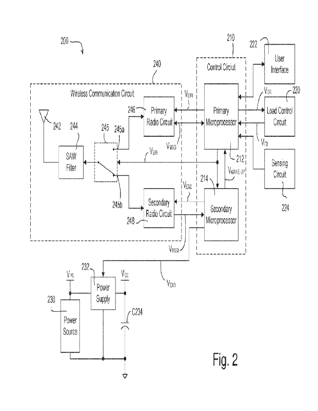
[0033] Fig. 2 is a block diagram of an example control
device 200, which may be deployed
in a load control system (e.g., the load control system 100 shown in Fig. 1).
The control device 200
may comprise a control circuit 210, which may include a first digital control
circuit, such a primary
microprocessor 212. The first digital control circuit may also comprise, for
example, a
microcontroller, a programmable logic device (PLD), an application specific
integrated circuit
(ASIC), a field-programmable gate array (FPGA), or any suitable processing
device or control
circuit. The control device 200 may comprise a memory (not shown) configured
to store operational
characteristics of the control device. The memory may be implemented as an
external integrated
circuit (IC) or as an internal circuit of the control circuit 210.
[0034] The control device 200 may comprise a load
control circuit 220 for controlling an
electrical load, e.g., an external and/or internal electrical load (not
shown). The primary
microprocessor 212 may be configured to generate one or more drive signals VDR
for controlling the
load control circuit 220 to control the electrical load (e.g., to turn the
electrical load on or off, and/or
to control the amount of power delivered to the electrical load). The primary
microprocessor 212
may also be configured to receive one or more feedback signals VFB (e.g.,
indicating the magnitude
of a load current conducted through the electrical load and/or a load voltage
developed across the
electrical load) from the load control circuit 220. For example, the control
device 200 may comprise
a dimmer switch (e.g., such as the dimmer switch 120 shown in Fig. 1) and the
load control circuit
may comprise a controllably conductive device, such as a thyristor (e.g.., a
triac) or one or more
field-effect transistors (FETs), coupled in series with a lighting load for
controlling the amount of
power delivered to the lighting load and thus an intensity of the lighting
load. In addition, the
control device 200 may comprise a light-emitting diode (LED) driver, and the
load control
circuit 220 may comprise an LED driver circuit for controlling the intensity
(e.g., brightness) and/or
color of one or more LED light sources. The control device 200 may also
comprise a motor drive
unit for a motorized window treatment, and the load control circuit 220 may
comprise a motor drive
circuit (e.g., an H-bridge drive circuit) for controlling a motor to adjust a
position of a covering
CA 03134994 2021- 10- 25
WO 2020/219984
PCT/US2020/029960
- 13 -
material of the motorized window treatment. For example, the feedback signals
VFB of the
motorized window treatment may be generated by a Hall-effect sensor circuit
and may indicate a
position of the covering material and/or direction of rotation of the motor.
[0035] The control device 200 may comprise a user
interface 222, which may comprise, for
example, one or more actuators (e.g., buttons) for receiving user inputs
and/or one or more visual
indicators for providing user feedback. For example, if the control device 200
comprises a
wall-mounted dimmer switch (e.g., such as the dimmer switch 120 shown in Fig.
1), the user
interface 220 may comprise a toggle actuator and an intensity adjustment
actuator (e.g., such as a
slider control or a pair of raise and lower buttons) for controlling a
lighting load. In addition, if the
control device 200 comprises a remote control device (e.g., such as the remote
control device 170
shown in Fig. 1), the user interface 222 may comprise one or more buttons for
controlling one or
more electrical loads, for example, by selecting preset (e.g., scenes) of the
load control system. The
user interface 222 may also comprise one or more light-emitting diodes (LEDs)
for illuminating the
visual indicators, for example, to provide a visual indication of a status
and/or a present intensity of a
lighting load, and/or a visual indication of a selected preset. The primary
microprocessor 212 of the
control circuit 210 may be configured to control the load control circuit 220
in response to actuations
of the actuators of the user interface 222, and may be coupled to the LEDs for
illuminating the visual
indicators to provide feedback.
[0036] The control device 200 may also comprise a
sensing circuit 224 configured to detect
and/or measure one or more environmental characteristics in the environment of
the control device.
For example, the sensing circuit 224 may comprise an occupancy detection
circuit configured to
detect an occupancy or vacancy condition in the vicinity of the control device
200. The sensing
circuit 224 may include a detector, such as, for example, a pyroelectric
infrared (PHI) detector, an
ultrasonic detector, and/or a microwave detector, for detecting an occupancy
or vacancy condition in
the vicinity of the control device 200. The control circuit 210 may be
configured to determine a
vacancy condition in the space after a timeout period expires since the last
occupancy condition was
detected. The control circuit 210 may be configured to control the load
control circuit 220 to control
the intensity of the electrical load in response to the sensing circuit 224
detecting occupancy and/or
vacancy conditions. The sensing circuit 224 may also comprise a daylight
sensing circuit (e.g.,
including a photodiode) for measuring an ambient light level in the space
around the control
CA 03134994 2021- 10- 25
WO 2020/219984
PCT/US2020/029960
- 14 -
device 200. In addition, the sensing circuit 224 may comprise a temperature
sensing circuit for
measuring a present temperature in the vicinity of the control device 200.
[0037] The control device 200 may comprise a power
source 230 (e.g., an internal power
source) for producing a direct-current (DC) voltage Vps. For example, the
power source 230 may
comprise one or more batteries and/or a photo-voltaic power source (e.g., a
solar cell). In addition,
the power source 230 may comprise one or more energy storage elements, such as
super capacitors
and/or rechargeable batteries, configured to charge from an external DC power
supply via a power
bus. The control device 200 may also comprise a power supply 232 that may
receive the DC
voltage Vps and generate a low-voltage DC supply voltage Vcc across a
capacitor C234 (e.g., an
energy storage capacitor) for powering the control circuit 210, the user
interface 222, the sensing
circuit 224, and other low-voltage circuitry of the control device 200. For
example, if the control
device 200 comprises a motor drive unit for a battery-powered motorized window
treatment, the
load control circuit 220 may receive power from the power source 230 (e.g.,
directly from the DC
voltage Vps), while the other circuitry may be powered from the DC supply
voltage Vcc. In
addition, the low-voltage circuitry of the control device 200 may also be
powered (e.g., directly
powered) from the DC voltage Vps produced by the power source (e.g., the
control device 200 may
not comprise the power supply 232). Further, the control device 200 may also
receive power from
an external power source, such as an alternating-current (AC) power source
(not shown). For
example, if the control device 200 comprises a dimmer switch (e.g., a two-wire
dimmer switch), the
power supply 232 may be electrically coupled in parallel with the controllably
conductive device of
the load control circuit 220 for conducting a charging current to generate the
DC supply voltage Vcc
when the controllably conductive device is non-conductive. The power supply
232 may also be
configured to conduct the charging current through an earth ground connection.
[0038] The control device 200 may comprise a wireless
communication circuit 240
configured to communicate (e.g., transmit and/or receive) wireless signals,
such as RF signals (e.g.,
the RF signals 108 shown in Fig. 1). The wireless communication circuit 240
may comprise an
antenna 242 for transmitting and receiving the RF signals and a surface
acoustic wave (SAW)
filter 244 (e.g., which may be optional). The wireless communication circuit
240 may comprise two
radio circuits: a primary radio circuit 246 (e.g., a first radio circuit) and
a secondary radio circuit 248
(e.g., a second radio circuit). The primary and secondary radio circuits 246,
248 may be coupled
CA 03134994 2021- 10- 25
WO 2020/219984
PCT/US2020/029960
- 15 -
(e.g., selectively and/or controllably coupled) to the SAW filter 244 via an
RF switch 245. The
primary microprocessor 212 may generate a switch control signal Vsw for
controlling the RF
switch 245 to be connected to a first contact 245a or a second contact 245k
The primary
microprocessor 212 may be configured to control the RF switch 245 to allow the
secondary radio
circuit 248 to monitor for transmitted RF signals most of the time (e.g., when
RF signals are not
being transmitted by other control devices) and then change to allow the
primary radio circuit 246 to
receive one of the RF signals (e.g., in response to the secondary radio
circuit 248 detecting an RF
signal), such that the primary radio circuit 246 is enabled (e.g., only
enabled) for short periods of
time (e.g., an RF signal is being transmitted by another control device).
[0039] The primary radio circuit 246 may comprise an RF
transceiver for transmitting and
receiving the RF signals via the antenna 242 when the RF switch 245 is
connected to the first
contact 245a. In addition, the primary radio circuit 246 may simply comprise
an RF receiver. The
primary radio circuit 246 may be coupled to the primary microprocessor 212 for
communicating
message signals VMSG (e.g., the digital messages transmitted and received via
the antenna 242) with
the primary microprocessor. The primary radio circuit 246 may be powered from
the DC supply
voltage Vcc. The primary radio circuit 246 may be configured to communicate RF
signals on one or
more communication channels (e.g., frequencies), which may be adjusted by the
primary
microprocessor 212. The primary radio circuit 246 may receive a first enable
control signal VENE
from the primary microprocessor 212 for enabling and disabling the primary
radio circuit 246 (e.g.,
controlling the primary radio circuit in and out of a sleep mode). The primary
microprocessor 212
may also be configured to enter a sleep mode when the primary radio circuit
246 is in the sleep
mode. The primary microprocessor 212 and the primary radio circuit 246 may
both be configured to
consume less power in the sleep more than when awake in a normal operation
mode. The primary
microprocessor 212 may be configured to control the load control circuit 220
to control the electrical
load in response to digital messages received from the primary radio circuit
246 via the message
signals VmSG. The primary microprocessor 212 may be configured to control the
visual indicators of
the user interface 222 in response to digital messages received from the
primary radio circuit 246 via
the message signals VmsG. The primary microprocessor 212 may be configured to
transmit digital
messages for controlling an electrical load via the primary radio circuit 246
in response to the user
interface 222 and/or the sensing circuit 224.
CA 03134994 2021- 10- 25
WO 2020/219984
PCT/US2020/029960
- 16 -
[0040] The secondary radio circuit 246 may comprise an
RF receiver for receiving the RF
signals via the antenna 242 when the RF switch 245 is connected to the second
contact 245b (e.g., as
shown in Fig. 2). For example, the secondary radio circuit 246 may comprise
part number
MAX7033, manufactured by Maxim Integrated. The secondary radio circuit 248 may
be powered
from the DC supply voltage Vcc. The secondary radio circuit 248 may be
characterized by a smaller
power dissipation (e.g., power consumption) than the primary radio circuit
246. For example, the
primary radio circuit 246 may be characterized by a typical power dissipation
of approximately
48 mW, while the secondary radio circuit 248 may be characterized by a typical
power dissipation of
approximately 19 mW. The secondary radio circuit 248 may be configured to
receive RF signals on
a single communication channel (e.g., frequency). The secondary radio circuit
248 may be
configured to generate a received signal strength identifier (RSSI) signal
VRssj, which may have a
magnitude that may indicate the signal strength of the RF signals received via
the antenna 242 when
the RF switch 245 is connected to the second contact 245b. The received signal
strength identifier
signal VRSST generated by the secondary radio circuit 248 may be characterized
by a fast stabilization
time (e.g., approximately 200-250 microseconds). In addition, the secondary
radio circuit 248 may
simply comprise a received signal strength measurement circuit. Further, the
secondary radio
circuit 248 may comprise an RF transceiver configured to generate the received
signal strength
identifier signal VRSSI.
[0041] The primary microprocessor 212 may be configured
to control the primary radio
circuit 246 in and out of the sleep mode in response to the secondary radio
circuit 214. The control
circuit 210 may comprise a second digital control circuit, such as a secondary
microprocessor 214,
for interfacing between the primary microprocessor 212 and the secondary radio
circuit 248. The
second digital control circuit may also comprise, for example, a
nrticrocontroller, a programmable
logic device (PLD), an application specific integrated circuit (ASIC), a field-
programmable gate
array (FPGA), or any suitable processing device or control circuit. The
secondary
microprocessor 214 may generate a wake-up control signal VwAKE-up for waking
up the primary
microprocessor 212 from the sleep mode_ For example, the wake-up control
signal VwAKE_up may be
received at an interrupt pin of the primary microprocessor 212. The secondary
microprocessor 214
may receive the received signal strength identifier signal VRssi generated by
the secondary radio
circuit 248 at an analog-to-digital converter (ADC) port of the secondary
microprocessor. The
CA 03134994 2021- 10- 25
WO 2020/219984
PCT/US2020/029960
- 17 -
secondary microprocessor 214 may generate a second enable control signal VEN2
for enabling and
disabling the secondary radio circuit 248 (e.g., controlling the secondary
radio circuit in and out of a
sleep mode during which the secondary radio circuit may consume less power).
The secondary
microprocessor 214 may also generate a third enable control signal VEN3 for
enabling and disabling
the power supply 232. When the secondary radio circuit 248 is in the sleep
mode (e.g., disabled),
the secondary microprocessor 214 may also be configured to enter a sleep mode
during which the
secondary microprocessor may consume less power. The secondary microprocessor
214 may be
configured to exit the sleep mode before (e.g., immediately before) enabling
the secondary radio
circuit 248 and enter the sleep mode after (e.g., immediate after) disabling
the secondary radio
circuit. The secondary microprocessor 214 may be configured to exit the sleep
mode in response to
an internal timer of the secondary microprocessor.
[0042] The secondary microprocessor 214 may be
configured to enable (e.g., periodically
enable) the secondary radio circuit 248 (e.g., approximately every 17.6
milliseconds), wait for a wait
time period TwArr (e.g., approximately 250 microseconds) until the magnitude
of the received signal
strength identifier signal VRSSI has stabilized (e.g., reached a steady state
value), and then sample the
received signal strength identifier signal VRSSI. If the magnitude of the
received signal strength
identifier signal VRSSlexceeds a threshold V-ru (e.g., indicating that the
magnitude of the received
RU signal exceeds approximately -90 dBm), the secondary microprocessor 214 may
determine that
an RU signal is presently being transmitted by another control device and may
control the wake-up
control signal VwAKE-up to wake up the primary microprocessor 212 from the
sleep mode into a
normal operation mode. After waking up, the primary microprocessor 212 may
control the switch
control signal Vsw to adjust the RF switch 245 from the second contact 245b to
the first
contact 245a., and control the first enable control signal Vii to wake up the
primary radio
circuit 246, such that the primary radio circuit 246 may receive RU signals
via the antenna 242. The
primary microprocessor 212 may be configured to enter the sleep mode after any
required processing
is complete, e.g., after transmitting and/or receiving of digital message is
complete and/or after any
processing required in response to a received digital message is complete. The
secondary
microprocessor 214 may also be configured to enter the sleep mode after the
primary
microprocessor 212 has entered the sleep mode.
CA 03134994 2021- 10- 25
WO 2020/219984
PCT/US2020/029960
- 18 -
[0043] Fig. 3 is a timing diagram illustrating example
waveforms of a control device (e.g.,
one of the control devices of the load control system 100 of Fig. 1 and/or the
control device 200 of
Fig. 2) during a data transmission event. For example, the data transmission
event may involve the
transmission of a particular digital message (e.g., including a command)
transmitted by a
transmitting device (e.g., the remote control device 170) to the control
device 200. During the data
transmission event, the transmitting device may transmit packets 300 (e.g.,
with each packet
including the same digital message and/or command) via RF signals (e.g., RF
signals 108). Each
packet 300 transmitted by the transmitting device may have a length equal to a
packet time
period TpAcKET (e.g., approximately 5 milliseconds). Each packet 300 may be
transmitted multiple
times (e.g., up to twelve times) during the data transmission event. For
example, four packets 300
are shown in Fig. 3 even though the data transmission event may include more
packets. Between
each packet 300, there may be a packet break time period TPKT-BRK (e.g.,
approximately
75 milliseconds), such that the transmitting device transmits packets of data
at a transmission rate of
approximately 12.5 packets per second. Alternatively, the break time period
TpKr_Bnic may not be a
fixed value, but may be a varying or random time between each of the
transmitted packets 300.
[0044] While the control device 200 is not receiving RF
signals (e.g., the packets 300) via
the wireless communication circuit 240, the primary microprocessor 212 and the
primary radio
circuit 246 may each be in the sleep mode. At this time, the first enable
control signal VEN 1 may be
low (e.g., at circuit common), which may cause the first radio circuit 246 to
be in the sleep mode. In
addition, the switch control signal Vsw may be low (e.g., at circuit common),
which may cause the
RF switch 245 to be connected to the second contact 245b. In addition, the
third enable control
signal VEN3 may be low (e.g., at circuit common), which may disable the power
supply 232. While
the power supply 232 is disabled, the primary microprocessor 212 and the
secondary
microprocessor 214 may draw a small amount of current from the capacitor C234.
[0045] The secondary microprocessor 214 may
periodically drive the second enable control
signal VEN2 high towards the DC supply voltage Vcc to periodically wake up the
secondary radio
circuit 248 to see if any control devices are presently transmitting one of
the packets 300. For
example, the secondary microprocessor 214 may enable the secondary radio
circuit 248 for a
sampling time period TSMPL-RF (e.g., approximately 300 microseconds) before
driving the second
enable control signal VEN2 low towards circuit common. The secondary
microprocessor 214 may
CA 03134994 2021- 10- 25
WO 2020/219984
PCT/US2020/029960
- 19 -
drive the second enable control signal VE42 high to start the sampling time
period TSMPL-RF
periodically according to a wake-up period TWAICE-UP (e.g., every 17.6
milliseconds). The secondary
radio circuit 248 may consume (e.g., only consume) significant power during
the sampling time
periods TSMPL-RF.
[0046] Prior to enabling the secondary radio circuit
248 during each sampling time
period TsmpL-Rp, the secondary microprocessor 214 may drive the third enable
control Signal VEN3
high to enable the power supply 232. For example, the secondary microprocessor
214 may drive the
third enable control signal VEN3 high to enable the power supply 232 at the
beginning of a power-
supply stabilization time period Tps-sm before driving the second enable
control signal VEN2 high to
enable the secondary radio circuit 248. The power-supply stabilization time
period TpS-STB may
allow the magnitude of the supply voltage Vcc to stabilize (e.g., reach a
steady-state value) before
the secondary radio circuit 248 is enabled. The secondary microprocessor 214
may keep the power
supply 232 enabled until the end of the sampling time period TsmpE-Rp, such
that the power supply is
periodically enabled for a power-supply enable time period Tps-EN.
[0047] During each sampling time period TsmpE_Rp, the
secondary microprocessor 214 may
wait for the wait time period TwAni to allow the magnitude of the received
signal strength identifier
signal VaSSI to stabilize before trying to determine if a packet 300 is being
transmitted during that
sampling time period. At the end of the wait time period TwArr, the secondary
microprocessor 214
may sample the received signal strength identifier signal VRSSE and compare
the sampled magnitude
to the threshold VTH to determine if a packet 300 is being transmitted during
the sampling time
period TsmpE_RE. If the secondary microprocessor 214 determines that a packet
300 is not being
transmitted during the RF sample time period TsfyipE_RE, the secondary
processor 214 may drive the
second enable control signal VEN2 low to cause the secondary radio circuit 248
to enter the sleep
mode for an RE sleep time period TsEp Rp. In addition, the secondary processor
214 may drive the
third enable control signal VEN3 low to disable the power supply 232 if the
secondary
microprocessor 214 determines that a packet 300 is not being transmitted
during the RE sample time
period TSMPL-RF.
[0048] If a packet 300 is being transmitted during the
RE sample time period TSMPL-RF, the
magnitude of the received signal strength identifier signal VRSSE may increase
from a minimum
CA 03134994 2021- 10- 25
WO 2020/219984
PCT/US2020/029960
- 20 -
magnitude (e.g., zero) to a steady-state magnitude Vss (e.g., as shown between
times to and ti in
Fig. 3). The secondary microprocessor 214 may wait for the wait time period
TwArr after driving the
second enable control signal VEN2 high (e.g., at time to) to allow the
magnitude of the received signal
strength identifier signal VRSSI to stabilize at the steady-state magnitude
Vss. The secondary
microprocessor 214 may then sample the received signal strength identifier
signal VRSSI at the end of
the wait time period TwArr (e.g., at time ti or slightly before time ti). If
the magnitude of the
received signal strength identifier signal VRSSI (e.g., the steady-state
magnitude Vss) is greater than
or equal to the threshold VIII, the secondary microprocessor 214 may drive the
wake-up control
signal VwAKE-up high towards the DC supply voltage Vcc for a pulse time period
TruLsE, before
subsequently driving the wake-up control signal VwARE-up low. The primary
microprocessor 212
does not go back to the sleep mode in response the wake-up control signal
VWARE-Ep being drive
low, but will enter the sleep mode after all necessary processing is complete.
The secondary
microprocessor 214 may also maintain the third enable control signal VEr./3
high to keep the power
supply 232 enabled after pulsing the wake-up control signal VWAKE-UP.
[0049] In response to detecting that the wake-up
control signal VWAKE-UP has been driven
high, the primary microprocessor 212 may wake up, drive the switch control
signal Vsw high to
change the RF switch 245 to the first contact 245a (e.g., as shown at time t2
in Fig. 3), and drive the
first enable control signal VENE high to wake-up the primary radio circuit 246
(e.g., as shown at
time t3 in Fig. 3). Since the primary radio circuit 246 is awake when the next
packet 300 is
transmitted (e.g., between times it and ts in Fig. 3), the primary radio
circuit 246 may be configured
to receive the packet 300 and the primary microprocessor 212 may be configured
to process and
respond to the packet. After the primary microprocessor 212 has processed the
packet and
determined that there are no more packets to transmit or receive and/or all
necessary processing in
response to the received digital message is complete, the primary
microprocessor 212 may drive the
first enable control signal VENE low (e.g., as shown at time t6 in Fig. 3).
The primary
microprocessor 212 may then drive the switch control signal Vsw low to change
the RF switch 245
back to the second contact 245b (e.g., as shown at time t7 in Fig. 3) before
entering the sleep mode.
In response to detecting that the switch control signal Vsw was driven low,
the secondary
microprocessor 214 may subsequently drive the third enable control signal VEN3
low to disable the
power supply 232 (e.g., as shown at time ts in Fig. 3). The secondary
microprocessor 214 may then
CA 03134994 2021- 10- 25
WO 2020/219984
PCT/US2020/029960
- 21 -
begin to periodically drive the second enable control signal VEN2 high during
the RF sample time
period TSMPL-RF once again to determine if any control devices are presently
transmitting another one
of the packets 300.
[0050] The RF sample time period TSMPL-RF and the RF
sleep time period TSLP-RF may be
sized appropriately to ensure that the RF sample time period TsmpirRE
coincides with at least one
packet 300 of a predetermined number of consecutive packets of a data
transmission event (e.g., as
described in greater detail in previously-referenced U.S. Patent No.
10,041,292). As a result, the RF
sleep time period TsLp-RF may be much longer than the packet time period
TpAcKET. In addition, the
RF sample time period TSMPL-RF may be significantly shorter than the packet
time period TPACKET.
For example, as shown in Fig. 3, the first two packets 300 do not coincide
with the RF sample time
period TSMPL-RF when the secondary radio circuit 248 is awake. At least a
portion of the third
packet 300 falls with the next RF sample time period TsmpL_RF, such that the
secondary
microprocessor 214 may be able to detect the packet and wake up the primary
microprocessor 212.
The primary microprocessor 212 may then wake up the primary radio circuit 246,
which is able to
receive the fourth packet 300. Since the secondary radio circuit 248
periodically wakes up to
determine if a packet is being transmitted (e.g., rather than the primary
radio circuit 246 waking up)
and the secondary radio circuit consumes less power than the primary radio
circuit, the control
device may have a significant power savings as compared to prior art control
devices having RF
receivers and/or transceivers.
[0051] While Figs. 2 and 3 show the primary
microprocessor 212 generating the switch
control signal Vsw for controlling the RF switch 245, the secondary
microprocessor 214 could also
generate the switch control signal Vsw. For example, after detecting that a
packet 300 is presently
being transmitted, the secondary microprocessor 214 may drive the wake-up
control signal VWAICE-UP
high to wake up the primary microprocessor 212 and drive the switch control
signal Vsw high to
change the RF switch 245 to the first contact 245a. The secondary
microprocessor 214 may cease
periodically enabling the secondary radio circuit 248 and maintain the switch
control signal Vsw
high while the primary radio circuit 246 is awake. The secondary
microprocessor 214 may drive the
switch control signal Vsw low to change the RF switch 245 to the second
contact 245b and begin
periodically enabling the secondary radio circuit 248 again in response to
receiving from the primary
microprocessor 212 an indication that the primary radio circuit 246 is in the
sleep mode (e.g., in
CA 03134994 2021- 10- 25
WO 2020/219984
PCT/US2020/029960
- 22 -
response to the switch control signal Vsw being driven low). In addition, the
RF switch 245 may be
controlled between the first contact 245a and the second contact 245b in
response to the wake-up
control signal VWAICE-UP and the secondary microprocessor 214 may be
configured to maintain the
wake-up control signal VwARE-op high while the primary radio circuit 246 is
awake (e.g., the switch
control signal Vsw may not be generated by either the primary microprocessor
212 or the secondary
microprocessor 214).
[0052] Fig. 4 is a flowchart of an example control
procedure 400 that may be executed by a
control circuit of a control device (e.g., the secondary microprocessor 214 of
the control device 200)
to periodically wake up a radio circuit (e.g., the secondary radio circuit
248) to determine if an RF
signal (e.g., a packet) is presently being transmitted. The control circuit
may generate a wake-up
signal VwAKE_up for causing another control circuit (e.g., the primary
microprocessor 212) to wake
up another radio circuit (e.g., the primary radio circuit 246). For example,
the control procedure 400
may be executed when the control device wakes up from a sleep mode at 410
(e.g., in response to an
internal timer of the control device). At 412, the control circuit may first
drive the second enable
control signal VE12 high to enable the secondary radio circuit 248. At 414,
the control circuit may
wait for a wait time period TwArr to allow the magnitude of the received
signal strength identifier
signal VISSI generated by the secondary radio circuit 248 to stabilize. The
control circuit may
sample the received signal strength identifier signal VRSM at 416 (e.g., at
the end of the wait time
period TwAtT). If the magnitude of the received signal strength identifier
signal VRSM is not greater
than or equal to a threshold VTH (e.g., indicating that the magnitude of the
received RF signal does
exceeds approximately -90 dBm) at 418, the control circuit may drive the
second enable control
signal VEN2 IOW at 420 and enter the sleep mode at 422, before the control
procedure 400 exits.
[0053] If the magnitude of the received signal strength
identifier signal VRsm is greater than
or equal to the threshold Vm (e.g., indicating that the magnitude of the
received RF signal exceeds
approximately -90 dBm) at 418, the control circuit may drive the wake-up
signal VwARE-up high for a
pulse time period TPULSE at 424. In response to detecting the pulse in the
wake-up signal VWAKE-UP,
the other control circuit (e.g., the primary microprocessor 212) may wake up
the other radio circuit
(e.g., the primary radio circuit 246). At 426, the control circuit may wait
until the other control
circuit indicates that the other radio circuit has been put back to sleep
(e.g., by determining when the
primary microprocessor 212 has driven the switch control signal Vsw low). When
the switch control
CA 03134994 2021- 10- 25
WO 2020/219984
PCT/US2020/029960
- 23 -
signal Vsw has been driven low at 426, the control circuit may then drive the
second enable control
signal VEN2 low at 420 and enter the sleep mode at 422, before the control
procedure 400 exits.
[0054] Fig. 5 is a flowchart of an example control
procedure 500 that may be executed by a
control circuit of a control device (e.g., the primary microprocessor 212 of
the control device 200) to
wake up a radio circuit (e.g., the primary radio circuit 246) and receive a
digital message (e.g., a
packet) via RE signals. The control circuit may execute the control produce
500 in response to
receiving a wake-up signal (e.g., the wake-up signal VwAKE-up from the
secondary
microprocessor 214) at 510. At 512, the control circuit may first drive the
switch control signal Vsw
high to adjust the RF switch 245 from the second contact 245b to the first
contact 245a (e.g., to
connect the primary radio circuit 246 to the antenna 242). At 514, the control
circuit may chive the
first enable control signal VENE high to enable the radio circuit. If the
control circuit receives a
message via the primary radio circuit 246 at 516 before a timeout expires at
518, the control circuit
may process the received message at 520. For example, the control circuit may
control a load
control circuit (e.g., the load control circuit 220) to control an electrical
load, illuminate visual
indicators (e.g., visual indicators of the user interface 222) to provide
feedback, and/or transmit a
message via the primary radio circuit 246 in response to the received message
at 520. The control
circuit may then drive the first enable control signal VEN1 low to cause the
primary radio circuit 246
to enter the sleep mode at 522. If the timeout expires at 518 before the
control circuit receive a
message at 516, the control circuit may simply put the primary radio circuit
246 in the sleep mode
at 522. At 524, the control circuit may drive the switch control signal Vsw
low at 524 to adjust the
RE switch 245 from the first contact 245a to the second contact 245b. At 526,
the control circuit
may enter the sleep mode, before the control procedure 500 exits.
[0055] While the control device 200 has been described
herein with the control circuit 210
comprising the primary microprocessor 212 and the secondary microprocessor
214, the functions of
the control circuit 210 could be implemented by a single microprocessor and/or
additional
microprocessors. In addition, the either or both of the primary microprocessor
212 and the
secondary microprocessor 214 may be implemented on a single integrated circuit
including either or
both of the primary radio circuit 246 and the secondary radio circuit 248. For
example, the primary
microprocessor 212 and the primary radio circuit 246 may be implemented on a
single integrated
circuit, and/or the secondary microprocessor 214 and the secondary radio
circuit 248 may be
CA 03134994 2021- 10- 25
WO 2020/219984
PCT/US2020/029960
- 24 -
implemented on a single integrated circuit. Further, the primary radio circuit
246 and the secondary
radio circuit 248 may be implemented in a single integrated circuit.
[0056] Although features and elements may be described
herein in particular combinations,
each feature or element may be used alone or in any combination with the other
features and
elements. While this disclosure has been described in terms of certain
embodiments and generally
associated methods, alterations and permutations of the embodiments and
methods will be apparent
to those skilled in the art. Accordingly, the above description of example
embodiments does not
constrain this disclosure. Other changes, substitutions, and alterations are
also possible without
departing from the spirit and scope of this disclosure.
CA 03134994 2021- 10- 25