Note: Descriptions are shown in the official language in which they were submitted.
CA 03135281 2021-10-06
Ultrasonic Imaging Device with Programmable Anatomy and Flow Imaging
BACKGROUND
[0001] Transducers in ultrasonic imagers transmit an ultrasonic beam
towards the
target to be imaged and a signal from the reflected waveform is used to create
an
image. The reflected waveform from tissue is used to form an image of the
anatomy
being viewed, whereas blood flow, velocity and direction of flow is measured
using
Doppler shift principles under electronic control.
BRIEF DESCRIPTION OF THE DRAWINGS
[0002] The accompanying drawings illustrate various examples of the
principles
described herein and are part of the specification. The illustrated examples
are given
merely for illustration, and do not limit the scope of the claims.
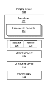
[0003] Fig. 1 illustrates a block diagram of an imaging device for anatomy
and flow
imaging, according to an example of the principles described herein.
[0004] Fig. 2 illustrates a diagram of a portable imaging system for
anatomy and
flow imaging, according to an example of the principles described herein.
[0005] Fig. 3 illustrates a schematic diagram of an imaging device with
imaging
capability, according to an example of the principles described herein.
[0006] Fig. 4 illustrates a side view of a curved transducer array,
according to an
example of the principles described herein.
[0007] Fig. 5 illustrates a top view of a transducer, according to an
example of the
principles described herein.
[0008] Fig. 6A illustrates an isometric view of an imaging device and scan
lines of a
frame, according to an example of the principles described herein.
[0009] Fig. 6B illustrates azimuth (xa), elevation (ya) and axial/depth
(za)
directions.
1
6961736
Date Recue/Date Received 2021-10-06
CA 03135281 2021-10-06
[0010] Fig. 6C illustrates beam focus and steering with changes in delay
for
elements on a column.
[0011] Fig. 6D illustrates a two-dimensional matrix of elements, where
relative
delays on columns are changed.
[0012] Fig. 7 illustrates the formation of a scan line, according to an
example of the
principles described herein.
[0013] Fig. 8 illustrates a flowchart of a method for selectively altering
a number of
channels of an imaging device, according to an example of the principles
described
herein.
[0014] Fig. 9 illustrates a receive channel, according to an example of the
principles described herein.
[0015] Fig. 10 illustrates a simplified schematic of a low-noise amplifier
(LNA) of a
receive channel, according to an example of the principles described herein.
[0016] Fig. 11 illustrates a circuit diagram of a fast power-up biasing
circuit,
according to an example of the principles described herein.
[0017] Fig. 12 illustrates the fabrication of a piezoelectric element,
according to an
example of the principles described herein.
[0018] Fig. 13 illustrates the fabrication of a piezoelectric element,
according to an
example of the principles described herein.
[0019] Fig. 14 illustrates the fabrication of a piezoelectric element,
according to an
example of the principles described herein.
[0020] Fig. 15 illustrates the fabrication of a piezoelectric element,
according to an
example of the principles described herein.
[0021] Fig. 16 illustrates the fabrication of a piezoelectric element,
according to an
example of the principles described herein.
[0022] Fig. 17A illustrates element construction for isolation to reduce
cross talk
between neighboring elements.
[0023] Fig. 17B illustrates element construction for isolation to reduce
cross talk
between neighboring elements.
[0024] Fig. 17C illustrates a cross-sectional view of a transducer element
connected to a corresponding application-specific integrated circuit (ASIC)
with at least
transmit drivers and receive amplifier electronics in the ASIC.
[0025] Fig. 18 illustrates a top view of a bottom electrode disposed on a
substrate
layer and arranged over a membrane, according to an example of the principles
described herein.
2
6961736
Date Recue/Date Received 2021-10-06
CA 03135281 2021-10-06
[0026] Fig. 19A illustrates a schematic diagram of a piezoelectric element,
according to another example of the principles described herein.
[0027] Fig. 19B illustrates a symbolic representation of the piezoelectric
element of
Fig. 19A, according to an example of the principles described herein.
[0028] Fig. 19C illustrates a cross-sectional view of a piezoelectric
element,
according to an example of the principles described herein.
[0029] Fig. 19D illustrates a cross-sectional view of two sub-elements
disposed on
a substrate, according to an example of the principles described herein.
[0030] Fig. 19E illustrates a cross-sectional view of two adjacent elements
showing
details of piezo layers, conductors and means of isolation, according to an
example of
the principles described herein.
[0031] Fig. 19F illustrates a cross-sectional view of two adjacent
elements, showing
isolation details to minimize cross talk, according to an example of the
principles
described herein.
[0032] Fig. 19G illustrates a cross-sectional view of two adjacent
elements, with
isolation details to minimize cross talk, according to an example of the
principles
described herein.
[0033] Fig. 19H illustrates a cross-sectional view of two adjacent
elements, with
isolation details to minimize cross talk, according to an example of the
principles
described herein.
[0034] Fig. 191 illustrates a piezoelectric element using flexural mode of
operation,
according to an example of the principles described herein.
[0035] Fig. 20A illustrates a scan line showing an ensemble of pulses,
according to
an example of the principles described herein.
[0036] Fig. 20B illustrates an imaging frame with multiple scan lines with
each line
showing multiple samples, according to an example of the principles described
herein.
[0037] Fig. 21 illustrates a transmit and receive operation using sub-
elements and
subsets to obtain an image, according to an example of the principles
described herein.
[0038] Fig. 22 illustrates an elevation plane being tilted and focused,
according to
an example of the principles described herein.
[0039] Fig. 23 illustrates an azimuth focus being altered electronically,
according to
an example of the principles described herein.
[0040] Fig. 24 illustrates a flow sensitive region in a Doppler sample
volume.
[0041] Throughout the drawings, identical reference numbers designate
similar, but
not necessarily identical, elements. The figures are not necessarily to scale,
and the
3
6961736
Date Recue/Date Received 2021-10-06
CA 03135281 2021-10-06
size of some parts may be exaggerated to more clearly illustrate the example
shown.
Moreover, the drawings provide examples and/or implementations consistent with
the
description; however, the description is not limited to the examples and/or
implementations provided in the drawings.
DETAILED DESCRIPTION
[0042] The present invention relates to imaging devices, and more
particularly to
portable handheld ultrasonic imaging devices having the ability to perform
flow and
anatomy imaging.
[0043] Ultrasound imaging (sonography) uses high-frequency sound waves to
view
inside the body. Because ultrasound images are captured in real-time, they can
also
show movement of the body's internal organs as well as blood flowing through
the
blood vessels. The sound waves are used to create and display images of
internal body
structures such as tendons, muscles, joints, blood vessels, and internal
organs.
[0044] To perform imaging, the imaging device transmits a signal into the
body and
receives a reflected signal from the body part being imaged. Types of imaging
devices
include transducers, which may also be referred to as transceivers or imagers,
and
which may be based on either photo-acoustic or ultrasonic effects. Such
transducers
can be used for imaging as well as other applications. For example,
transducers can be
used in medical imaging to view anatomy of tissue or other organs in a body.
Transducers can also be used in industrial applications such as materials
testing or
therapeutic applications such as local tissue heating of HIFU based surgery.
When
imaging a target and measuring movement of the target, such as flow velocity
and
direction blood, Doppler measurements techniques are used. Doppler techniques
are
also applicable for industrial applications to measure flow rates, such as
fluid or gas
flow in pipes.
[0045] The difference between transmitted and reflected wave frequencies
due to
relative motion between the source and the object is known as a Doppler
effect. The
frequency shift is proportional to the movement speed between the transducer
and the
object. This effect is exploited in ultrasound imaging to determine blood flow
velocity
and direction.
[0046] Doppler imagers may generate either continuous wave (CW) or a pulsed
wave (PW) ultrasound beam. In CW Doppler, signals are continuously transmitted
and
received, requiring two element transducers, one for transmitting and another
for
4
6961736
Date Recue/Date Received 2021-10-06
CA 03135281 2021-10-06
receiving. In PW operation, a single-element transducer is used for
transmitting and
receiving the ultrasound signals.
[0047] For ultrasound imaging, transducers are used to transmit an
ultrasonic
beam towards the target to be imaged. A reflected waveform is received by the
transducer, converted to an electrical signal and with further signal
processing, an
image is created. Velocity and direction of flow may be measured using an
array of
micro-machined ultrasonic transducers (MUTs).
[0048] B-mode imaging for anatomy is a two-dimensional ultrasound image
display
composed of dots representing the ultrasound echoes. The brightness of each
dot is
determined by the amplitude of the returned echo signal. This allows for
visualization
and quantification of anatomical structures, as well as for the visualization
of diagnostic
and therapeutic procedures. Usually, the B-mode image bears a close
resemblance to
the actual anatomy of a cutout view in the same plane. In B-mode imaging, a
transducer is first placed in a transmit mode and then placed in receive mode
to receive
echoes from the target. The echoes are signal processed into anatomy images.
The
transducer elements are programmable such that they can be either in transmit
mode
or in receive mode, but not simultaneously.
[0049] The use of color flow Doppler, color Doppler imaging, or simply
color
Doppler allows the visualization of flow direction and velocity for blood in
an artery or
vein within a user defined area. A region of interest is defined, and the
Doppler shifts of
returning ultrasound waves are color-coded based on average velocity and
direction.
Sometimes these images are overlapped (co-imaged) with anatomy images in B-
mode
scan to present a more intuitive feel of flow relative to anatomy being
viewed. Doppler
imaging can also be PW Doppler so that the range and velocity of flow is
determined,
but maximum flow rate is dependent on pulse repetition frequency used,
otherwise
images are aliased making higher velocities look like lower velocities.
Doppler shift can
be measured from an ensemble of waves received to measure flow velocity using
PW
mode of Doppler imaging. CW Doppler is a continuous imaging technique where
aliasing is avoided through continuous transmitting from one transducer
element while
receiving echoes from another transducer element. With this technique, the
range is
ambiguous. In a programmable instrument, both pulsed and continuous techniques
can
be implemented as discussed later. PW and Color Doppler may use a selected
number
of elements in an array. First, the elements are placed in a transmit mode and
after
echoes have returned, the elements are placed in a receive mode where the
received
signal is processed for Doppler signal imaging. For CW Doppler, at least two
different
6961736
Date Recue/Date Received 2021-10-06
CA 03135281 2021-10-06
elements are utilized, where each element is in transmit mode while the other
element
is in receive mode continuously.
[0050] The Doppler signal from a moving object contains not only
information about
flow, but also backscatter signals containing clutter that originates from
surrounding
tissue or slowly moving vessels. This clutter signal may be typically 40 to 80
dB
stronger than the Doppler shift signal originating from blood. Thus, a clutter
rejection is
needed to estimate the flow accurately. Clutter suppression is a step in the
processing
of Doppler signal. A high pass filter (HPF) may be used to remove the clutter
signal
from the Doppler shift signal. A high pass filter is used to suppress signals
from
stationary or slow-moving tissue or any other organs. Signals from slow moving
objects
are of low-frequency, but they may have amplitudes much stronger than high
frequency
signals generated from the faster blood flow. Thus, for separating the signals
from
blood and tissue, a high pass filter with a sharp transition band is used.
These filters
can be developed digitally in the receiver. These filters, sometimes known as
Wall
filters, look at the difference in signals from different transmissions, with
the signals
aligned in phase. Any deviation caused by Doppler shift is the desired output.
However,
if low frequency clutter causes some of this deviation, the sensitivity of the
flow
detection algorithm becomes degraded. Effects from switched mode dc to dc
converter-
based power supplies may cause clock frequency and harmonics to show up in the
power supply. Further, these frequencies can create other frequencies due to
interaction of other switching phenomena, for example, pulse repetition rate
of the
Doppler sequence.
[0051] To the extent that these kinds of behavior or intermodulation
behavior are
caused by nonlinearities, spurious signals show up in the frequencies of
interest for
flow imaging and sensitivity of flow imaging is reduced. Another example of
clutter is
amplitude jitter of the pulses used in the transmit pulsar. One source of the
clutter may
be the power supply amplitudes varying from pulse to pulse, due to the power
supply
capacitors being drained of charge to deliver current during a pulse and not
getting
recharged to a same level for the next pulse.
[0052] In addition to use of digital Wall filters, low frequency content
causing clutter
can be minimized by using a high pass filter ahead of the digital filter.
Filters can be in
the analog domain and also in the digital domain. A part of these filters can
also be
performed right at the transducer interface, where real time control of high
pass
frequency is achieved by controlling the radio frequency (Rf) and carrier
frequency
(CHF) network. Radio frequency (Rf) refers to the rate of oscillation of
electromagnetic
6
6961736
Date Recue/Date Received 2021-10-06
CA 03135281 2021-10-06
radio waves in the range of 3 kHz to 300 GHz, as well as the alternating
currents
carrying the radio signals. Carrier frequency (CHF) is defined as the
transmission of a
fixed frequency that has been altered or otherwise modulated to carry data.
This
achieves a 20dB/Dec high pass slope.
[0053] Additionally, beyond use of a low noise amplifier (LNA), other
digitally
controlled high pass filters (HPF) can be leveraged to simplify operations in
the receiver
to save power and processing time. By rejecting unneeded clutter before time
gain
compensation (TGC), an LNA increases the dynamic range of the signal presented
to
an analog to digital converter (ADC). The digitized bits can now be processed
for
further Doppler operations.
[0054] The acquisition of Doppler relies on repeated transmission of pulses
to
acquire data from a particular region of interest. Such acquisition is precise
in its
periodicity to ensure that the Doppler signal is uniformly sampled for further
spectrogram processing. This can be a major constraint to ultrasound imaging
systems
when this Doppler signal acquisition is done in such modes as Duplex or
Triplex
imaging where B-mode or color flow signals are acquired concurrently. This
constraint
reduces the frame rates for other modes and hence limits the ability of the
sonographer
to follow events in real-time. Moreover, the rapid periodic transmission of
ultrasound
pulses to the same location can increase the average power per unit area
beyond
certain safety standards and therefore limitations on acoustic power generated
drive
close attention to keep this in the safe zone.
[0055] Doppler shift principles are used to calculate the blood flow
velocity. Other
types of velocity can be calculated, such as body fluids, industrial fluids,
gases, etc.
When the observer moves towards the source, the increased frequency, fr, due
to
passing more wave cycles per seconds, is given by:
fr = ft c-cv
[0056] In the above, ft is the transmitted frequency, c is the velocity of
sound in
tissue, and v is the velocity of the observer (for example, blood).
[0057] The velocity is replaced by the component of velocity in the wave
direction,
v cos 0, if the velocity of the observer is at an angle 0 to the direction of
the wave
propagation.
7
6961736
Date Recue/Date Received 2021-10-06
CA 03135281 2021-10-06
C VCOS0
fry - ft C
[0058] If the observer is at rest and the source moves with the velocity in
the
direction of wave travel, the wavelengths are compressed. The resulting
observed
frequency is:
fry = ftC12
[0059] Taking the angle into account:
fry_ ft C
C-VCOS0
[0060] In application of ultrasound, an ultrasonic beam is backscattered
from the
moving blood cells and tissue. Both of the above effects combine to give the
transmitted Doppler shift in frequency. The observed frequency is then given
by:
- c+vcoso * C - c+vcoso
frY ft C ft
c-vcoso c-vcoso
[0061] As mentioned, the Doppler shift frequency is the difference between
incident
frequency ft and reflected frequency fr, and is therefore given by:
fa = f -- ft
c+vcoso
fa ¨ ft ft
c¨vcoso
[0062] Since c>> v
fa = 2*-tv coso
C
[0063] From the last relationship, the Doppler shift depends on the angle 0
to the
direction of the propagation and the transmitted frequency.
[0064] The best reflection takes place when measuring at 90 degrees to the
electronically steered in the azimuth and elevation plane to achieve optimal
Doppler
8
6961736
Date Recue/Date Received 2021-10-06
CA 03135281 2021-10-06
signal detection. This elevation steering is controlled by a combination of
elevation
delay control along with any desired azimuth.
[0065] A continuous wave Doppler system is a system that sends and receives
a
continuous ultrasound wave by using two separate transducer elements housed
within
the same probe. Because transmission and reception are continuous, the system
has
no depth resolution, except in the sense that signals originating from close
to the
transducer experience less attenuation than those from a distant target. The
transmitted 2112 and received beams 2114 are shown in a Doppler sample volume
in
Fig. 24. The flow sensitive zone 2116 over which Doppler information can be
acquired
(sample volume) is the region of transmitting and receiving beam overlap as
indicated
by cross-hatched lines that occur at some distance from the transducer face.
[0066] It is possible to construct an element that includes two sub-
elements for
example, where one can be in transmit mode and the other in receive mode. By
using
embedded dual sub-elements instead of a single element in the transducer, the
entire
transducer area or portions selected thereof can be used for transmission and
reception. Also, areas of intersection are increased by use of dual sub-
elements.
[0067] Imaging devices such as ultrasound imagers used in medical imaging
use
piezoelectric (PZT) material or other piezo ceramic and polymer composites. To
fabricate the bulk PZT elements for the transducers, a thick piezoelectric
material slab
can be cut into large rectangular shaped PZT elements. The rectangular-shaped
PZT
elements are expensive to build, since the manufacturing process involves
precise
cutting of the rectangular-shaped thick PZT or ceramic material and mounting
it onto
substrates with precise spacing. Furthermore, the impedance of the transducers
is
much higher than acoustic impedance of tissue, which requires use of impedance
matching layers to allow for practical transmission and reception of signals.
[0068] Still further, such thick bulk PZT elements can require relatively
high voltage
pulses. For example, 100 volts (V) or more may be required to generate
transmission
signals. High drive voltage results in high power dissipation since the power
dissipation
in the transducers is proportional to the square of the drive voltage. The
high power
dissipation generates heat within the imaging device such that cooling
arrangements
are necessitated. The use of cooling systems increases the manufacturing costs
and
weights of imaging devices which makes the imaging devices more burdensome to
operate. High voltages also increase the cost of electronics.
[0069] Even further, the transmit/receive electronics for the transducers
may be
located far away from the transducers themselves, thus requiring micro-coaxial
cables
9
6961736
Date Recue/Date Received 2021-10-06
CA 03135281 2021-10-06
between the transducers and transmit/receive electronics. In general, the
cables have a
precise length for delay and impedance matching, and, quite often, additional
impedance matching networks are used for efficient connection of the
transducers
through the cables to the electronics.
[0070] Accordingly, the present specification describes the use of
piezoelectric
micromachined ultrasound transducers (pMUTs), which can be efficiently formed
on a
substrate leveraging various semiconductor wafer manufacturing operations.
Semiconductor wafers may come in 6 inch, 8 inch, and 12 inch sizes and are
capable
of housing hundreds of transducer arrays. These semiconductor wafers start as
a
silicon substrate on which various processing steps are performed. An example
of such
an operation is the formation of 5i02 layers, also known as insulating oxides.
Various
other steps such as the addition of metal layers to serve as interconnects and
bond
pads or copper pillars may be used to allow connections of the pMUTs to other
electronics. Also, use of etching techniques to create cavities in the silicon
structure
allows formation of membranes that can move under electrical control or due to
external pressure inputs. Compared to the conventional transducers having
bulky
piezoelectric material, pMUTs built on semiconductor substrates are less
bulky, are
cheaper to manufacture, and have simpler and higher performance
interconnection
between electronics and transducers. As such, they provide flexibility in the
operational
frequency, and potential to generate higher quality images due to lower
parasitics in the
interconnection.
[0071] In one example, the imaging device is coupled to an application
specific
integrated circuit (ASIC) that includes transmit drivers, sensing circuitry
for received
echo signals, and control circuitry to control various operations. The ASIC
can be
formed on a separate semiconductor wafer and the pMUT on another wafer. Also,
the
ASIC can be placed in close proximity to pMUT elements to reduce parasitic
losses. In
one example, the ASIC may be 50 micrometers (pm) or less away from the
transducer
array. There may be less than a 100 pm separation between the 2 wafers or 2
die,
where each wafer includes many dies and a die includes a transducer in the
transducer
wafer and an ASIC in the ASIC wafer. The ASIC may have matching dimensions
relative to the pMUT to allow the devices to be stacked for wafer-to-wafer
interconnection or transducer die on ASIC wafer or transducer die to ASIC die
interconnection. Alternatively, the transducer can be developed on top of the
ASIC
wafer using low temperature piezo material sputtering and other low
temperature
processing compatible with ASIC processing.
6961736
Date Recue/Date Received 2021-10-06
CA 03135281 2021-10-06
[0072] While pMUTs have potential for advanced ultrasonic imaging, some
limitations have impeded their utilization in high performance imaging
implementation.
As an example, pMUTs utilizing Aluminum Nitride exhibit low sensitivity
related to
transmit and receive operations making them candidates for less demanding
applications. Other pMUTs utilizing PZT require relatively high voltages and
exhibit
relatively low bandwidth and low efficiency.
[0073] Accordingly, the present specification describes pMUTs that 1) have
an
enhanced sensitivity, 2) may operate at low voltages, 3) exhibit high
bandwidth
operation, and 4) exhibit good linearity. Specifically, the present
specification describes
pMUTs in close proximity to the associated control circuitry. This allows 2D
and 3D
imaging under control of a control circuitry in a small portable device.
[0074] Another type of transducer is a capacitive micromachine ultrasonic
transducer (cMUT). However, cMUT sensors have difficulty with generating
sufficient
acoustic pressure at lower frequencies (where the bulk of deep medical imaging
occurs) compared to PZT based devices and are inherently nonlinear.
Furthermore,
cMUTs require high voltage operation.
[0075] In general, an imaging device of the present specification includes
a number
of transmit channels and a number of receive channels. Transmit channels drive
the
piezoelectric elements with a voltage pulse at a frequency the elements are
responsive
to. This causes an ultrasonic waveform to be emitted from the piezoelectric
elements
which waveform is directed towards an object to be imaged. In some examples,
the
imaging device with the transducer array of piezoelectric elements makes
mechanical
contact with the body using a gel in between the imaging device and the body.
The
ultrasonic waveform travels towards the object, i.e., an organ, and a portion
of the
waveform is reflected back to the piezoelectric elements, where the received
ultrasonic
energy is converted to an electrical energy, which is then further processed
by a
number of receive channels and other circuitry to develop an image of the
object.
[0076] These transmit and receive channels consume power and in instruments
where there are many channels (to generate high quality images), the power may
cause excessive heat buildup in the imaging device. If the temperature rises
past a
certain value, it may affect operation of the imaging device, could pose a
danger to the
operator, could pose a danger to a patient, and may be outside of regulatory
specifications which restrict how high the temperature can rise. An ultrasound
imaging
device includes a transducer array, an ASIC, transmit and receive beamforming
circuitry, and control electronics. Specifications restrict the maximum
temperature that
11
6961736
Date Recue/Date Received 2021-10-06
CA 03135281 2021-10-06
can be tolerated, which in turn, severely restricts which electronic circuits
can be
housed in the imaging device and also restricts how the imaging device is
operated.
Such restrictions can negatively affect the image quality achieved and the
frame rate of
images. Furthermore, imaging devices may be battery-powered which may drain
quickly in instruments with many channels as each channel draws energy.
[0077] The imaging device of the present disclosure resolves these and
other
issues. Specifically, the imaging device controls power dissipation without
exceeding
temperature limits of the imaging device all while maintaining needed image
quality.
Specifically, the number of receive channels and/or transmit channels used to
form an
image are electronically adaptable to save power, for example, in cases where
a lower
number of channels is acceptable. As a specific example, each of the number of
channels may be dynamically controlled to reduce power, or to be powered down
entirely. Additionally, other characteristics of each channel are also
configurable to
reduce power. Such advanced control allows the imaging device to be operated
within
safe temperature thresholds, and may do so without materially sacrificing
needed
image quality. The lower power consumption also increases battery life.
[0078] Also, the imaging device includes a handheld casing where
transducers and
associated electronics are housed. The imaging device may also contain a
battery to
power the electronics. As described above, the amount of power consumed by the
imaging device increases the temperature of the imaging device. To ensure
satisfactory
use of the imaging device and imaging device performance, the temperature of
the
body of the imaging device should remain below a threshold temperature. The
imaging
device of the present specification is electronically configured to reduce
power and
temperature notwithstanding the acquisition of high quality images which
consumes a
significant amount of power, reduces battery life, and increases temperature
in the
probe.
[0079] In one example, the present disclosure describes a high performance,
low
power, and low cost portable imaging device capable of 2D and 3D imaging using
pMUTs in a 2D array built on a silicon wafer. Such an array coupled to an ASIC
with
electronic configuration of certain parameters enables a higher quality of
image
processing at a lower cost than has been previously possible. By controlling
certain
parameters, such as the number of channels used or the amount of power used
per
channel, power consumption can be altered and temperature can be changed.
[0080] The present disclosure describes an imaging device that relies on
pMUT-
based transducers connected to control electronics on a per pixel basis and
housed in
12
6961736
Date Recue/Date Received 2021-10-06
CA 03135281 2021-10-06
a portable housing. The imaging device allows system configurability and
adaptability in
real time to actively control power consumption and temperature in the imaging
device.
Flow imaging, in particular, can consume more power than anatomy imaging
modes.
Power is reduced by minimizing power dissipation within the imaging device by
1)
altering the aperture size and/or 2) actively controlling power dissipation in
those
channels such that temperatures within the imaging device do not exceed
specification
limits. All this is done while achieving superior performance than would
otherwise be
possible. Further, acoustic power output can increase in Doppler modes
compared to
other anatomy modes. Electronic means are provided to control such power
output
levels.
[0081] The manufacturing cost of pMUTs described herein may be reduced by
applying modern semiconductor and wafer processing techniques. For example, a
thin
film piezoelectric layer may be spun on or sputtered onto semiconductor wafers
and
later patterned to create piezoelectric sensors that each have two or more
electrodes.
In one example, each piezoelectric element may be designed to have the ability
to emit
or receive signals at a certain frequency, known as the center frequency, as
well as the
second and/or additional frequencies. Note that the term piezoelectric
element, pMUT,
transceiver, and pixel are used herein interchangeably.
[0082] In one example, an imaging device includes a transducer that has an
array
of piezoelectric elements that are formed on a substrate. Each of the
piezoelectric
elements include at least one membrane suspended from the substrate, at least
one
bottom electrode disposed on the membrane, at least one piezoelectric layer
disposed
on the bottom electrode, and at least one top electrode disposed on the at
least one
piezoelectric layer. Adjacent piezoelectric elements are configured to be
isolated
acoustically from each other.
[0083] In another example, an imaging device includes a transducer with a
two-
dimensional (2D) array of piezoelectric elements arranged in rows and columns
on the
transducer. Each piezoelectric element has at least two terminals and is
physically
isolated from each adjacent piezoelectric element to minimize cross talk. A
first set of
piezoelectric elements of the array includes that each piezoelectric element
has a first
top electrode connected to a respective receive amplifier and is
electronically
programmed as if connected together to form a first column. A second set of
piezoelectric elements of the array includes that each piezoelectric element
has a
second top electrode connected to a respective transmit driver and is
electronically
programmed as if connected together to form a second column.
13
6961736
Date Recue/Date Received 2021-10-06
CA 03135281 2021-10-06
[0084] In another example, an imaging device includes a transducer and a 2D
array of piezoelectric elements arranged in rows and columns on the
transducer. Each
piezoelectric element has at least two terminals. At least a first column of
the
piezoelectric elements includes that each piezoelectric element has a first
top electrode
connected to a respective receive amplifier or a transmit driver under
programmed
control. At least a second column of the piezoelectric elements includes that
each
piezoelectric element has a first top electrode connected to a respective
receive
amplifier or transmit driver under programmed control. The piezoelectric
elements are
programmed to transmit and then subsequently receive or to simultaneously
transmit
and receive.
[0085] Turning now to the figures, Fig. 1 illustrates a block diagram of an
imaging
device (100) with transmit (106) and receive channels (108), controlled by
control
circuitry (109), and having imaging computations performed on a computing
device
(110) according to principles described herein. Fig. 1 further includes a
power supply
(111) to energize the various components in the imaging device (100).
[0086] As described above, the imaging device (100) may be used to generate
an
image of internal tissue, bones, blood flow, or organs of human or animal
bodies.
Accordingly, the imaging device (100) transmits a signal into the body and
receives a
reflected signal from the body part being imaged. Such imaging devices (100)
include
piezoelectric transducers (102), which may be referred to as transceivers or
imagers,
which may be based on photo-acoustic or ultrasonic effects. The imaging device
(100)
can be used to image other objects as well. For example, the imaging device
(100) can
be used in medical imaging, flow measurements for fluids or gases in pipes,
lithotripsy,
and localized tissue heating for therapeutic and highly intensive focused
ultrasound
(HIFU) surgery.
[0087] In addition to use with human patients, the imaging device (100) may
be
used to get an image of internal organs of an animal as well. Moreover, in
addition to
imaging internal organs, the imaging device (100) may also be used to
determine
direction and velocity of blood flow in arteries and veins, as well as tissue
stiffness, with
Doppler mode imaging.
[0088] The imaging device (100) may be used to perform different types of
imaging. For example, the imaging device (100) may be used to perform one
dimensional imaging, also known as A-Scan, 2D imaging, also known as B scan (B-
mode), three dimensional (3D) imaging, also known as C scan, and Doppler
imaging.
14
6961736
Date Recue/Date Received 2021-10-06
CA 03135281 2021-10-06
The imaging device (100) may be switched to different imaging modes and
electronically configured under program control.
[0089] To facilitate such imaging, the imaging device (100) includes an
array of
piezoelectric transducers (102), each piezoelectric transducer (102) including
an array
of piezoelectric elements (104). A piezoelectric element (104) may also
include two of
more sub-elements, each of which may be configurable in a transmit or receive
operation. The piezoelectric elements (104) operate to 1) generate the
pressure waves
that are passed through the body or other mass and 2) receive reflected waves
off the
object within the body, or other mass, to be imaged.
[0090] In some examples, the imaging device (100) may be configured to
simultaneously transmit and receive ultrasonic waveforms. For example, certain
piezoelectric elements (104) may send pressure waves toward the target object
being
imaged while other piezoelectric elements (104) receive the pressure waves
reflected
from the target object and develop electrical charges in response to the
received
waves.
[0091] In some examples, each piezoelectric element (104) may emit or
receive
signals at a certain frequency, known as a center frequency, as well as the
second
and/or additional frequencies. Such multi-frequency piezoelectric elements
(104) may
be referred to as multi-modal piezoelectric elements (104) and can expand the
bandwidth of the imaging device (100).
[0092] The piezoelectric material that forms the piezoelectric elements
(104)
contracts and expands when different voltage values at a certain frequency are
applied.
Accordingly, as voltages alternate between different values applied, the
piezoelectric
elements (104) transform the electrical energy (i.e., voltages) into
mechanical
movements resulting in acoustic energy which is emitted as waves at the
desired
frequencies. These waves are reflected from a target being imaged and are
received at
the same piezoelectric elements (104) and converted into electrical signals
that are
then used to form an image of the target.
[0093] To generate the pressure waves, the imaging device (100) includes a
number of transmit channels (106) and a number of receive channels (108). The
transmit channels (106) include a number of components that drive the
transducer
(102), (i.e., the array of piezoelectric elements (104)), with a voltage pulse
at a
frequency that they are responsive to. This causes an ultrasonic waveform to
be
emitted from the piezoelectric elements (104) towards an object to be imaged.
The
ultrasonic waveform travels towards the object to be imaged and a portion of
the
6961736
Date Recue/Date Received 2021-10-06
CA 03135281 2021-10-06
waveform is reflected back to the transducer (102), where the receive channels
(108)
collect the reflected waveform, convert it to an electrical energy, and
process it, for
example, at the computing device (110), to develop an image that can be
displayed.
[0094] In some examples, while the number of transmit channels (106) and
receive
channels (108) in the imaging device (100) remain constant, the number of
piezoelectric elements (104) that they are coupled to may vary. This coupling
is
controlled by the control circuitry (109). In some examples, a portion of the
control
circuitry (109) may be distributed in the transmit channels (106) and in the
receive
channels (108). For example, the piezoelectric elements (104) of a transducer
(102)
may be formed into a 2D array with N columns and M rows.
[0095] In one example, the 2D array of piezoelectric elements (104) have a
number
of columns and rows, such as 128 columns and 32 rows. The imaging device (100)
may have up to 128 transmit channels (106) and up to 128 receive channels
(108).
Each transmit channel (106) and receive channel (108) is coupled to multiple
or single
piezoelectric elements or sub-elements (104). Depending on the imaging mode,
each
column of piezoelectric elements (104) may be coupled to a single transmit
channel
(106) and a single receive channel (108). The transmit channel (106) and
receive
channel (108) receive composite signals, which composite signals combine
signals
received at each piezoelectric element (104) within the respective column.
[0096] In another example, (i.e., during a different imaging mode),
individual
piezoelectric elements (104) are coupled to their own transmit channel (106)
and their
own receive channel (108).
[0097] In other examples, the computing device 110 or power supply and
battery
111 are external.
[0098] Fig. 2 is a diagram of an imaging system with flow imaging
capability along
with anatomy imaging capability, according to an example of the principles
described
herein. As depicted, the imaging system includes the imaging device (100) that
generates and transmits, via the transmit channels (Fig. 1, 106) pressure
waves (210)
toward an internal organ, such as a heart (214), in a transmit mode/process.
The
internal organ, or other object to be imaged, may reflect a portion of the
pressure
waves (210) toward the imaging device (100) which captures, via the transducer
(Fig
1,102), receive channels (Fig. 1, 108), control circuitry (Fig. 1, 109), the
computing
device (Fig 1,110), and the reflected pressure waves, and generates electrical
signals
in a receive mode/process. The system also includes another computing device
(216)
that communicates with the imaging device (100) through a communication
channel
16
6961736
Date Recue/Date Received 2021-10-06
CA 03135281 2021-10-06
(218). The imaging device (100) may communicate electrical signals to the
computing
device (216) which processes the received signals to complete formation of an
image
of the object. A display device (220) of the system can then display images of
the organ
or target including images that show blood flow related images in the targeted
areas.
[0099] As depicted in Fig. 2, the imaging device (100) may be a portable,
handheld
device that communicates signals through the communication channel (218),
either
wirelessly (using a protocol, such as 802.11 protocol) or via a cable (such as
universal
serial bus 2 (USB2), USB 3, USB 3.1, and USB-C), with the computing device
(216). In
the case of a tethered connection, the imaging device (100) may include a port
as
depicted in Fig. 3 for receiving the cable that is to communicate with the
computing
device (216). In the case of a wireless connect, the imaging device (100)
includes a
wireless transmitter to communicate with the computing device (216).
[00100] The display device (220) and the computing device (216) may be
separate
from the imaging device (100) as shown. For example, the computing device
(216) and
display device (220) may be disposed within a separate device (e.g., a mobile
device,
such as cell phone or iPad, or a stationary computing device), which can
display
images to a user. In another example, the display device (220) and the
computing
device (220) are contained within the imaging device (100). That is, the
imaging device
(100), computing device (216), and display device (220) are disposed within a
single
housing.
[00101] Fig. 3 is a schematic diagram of an imaging device (100) with flow
and
anatomy measurement capability, according to an example of the principles
described
herein. As described above, the imaging device (100) may be an ultrasonic
medical
probe. Fig. 3 depicts the transducer(s) (102) of the imaging device (100). As
described
above, the transducer(s) (102) include an array of piezoelectric elements
(Fig. 1, 104)
that transmit and receive pressure waves (Fig. 2, 210). In some examples, the
imaging
device (100) includes a coating layer (322) that serves as an impedance
matching
interface between the transducers (102) and the human body, or other mass
through
which the pressure waves (Fig. 2, 210) are transmitted. In some cases, the
coating
layer (322) may serve as an impedance matching layer and also a lens when
designed
with a curvature consistent with a desired focal length. The coating layer
(322) may
consist of several layers of materials, some of which are used for impedance
matching
the transducer to tissue acoustic impedance and some of which are shaped into
a
mechanical lens to focus the acoustic signals in the elevation direction.
17
6961736
Date Recue/Date Received 2021-10-06
CA 03135281 2021-10-06
[00102] In embodiments, the user may apply gel on the skin of the human body
before a direct contact with the coating layer (322) so that the impedance
matching at
the interface between the coating layer (322) and the human body may be
improved.
Impedance matching reduces the loss of the pressure waves (Fig. 2, 210) at the
interface and the loss of the reflected wave traveling toward the imaging
device (100) at
the interface.
[00103] In some examples, the coating layer (322) may be a flat layer to
maximize
transmission of acoustic signals from the transducer(s) (102) to the body and
vice
versa. Certain parts of the coating layer (322) may be a quarter wavelength in
thickness
at a certain frequency of the pressure wave (Fig. 2, 210) generated or
received by the
transducer(s) (102).
[00104] The imaging device also includes control circuitry (109), such as an
ASIC,
for controlling the transducers (102). The control circuitry (109) may be
housed in an
ASIC along with other circuitry which is coupled to the transducers (102) by
bumps that
connect transducers (102) to the ASIC. As described above, the transmit
channels
(106) and receive channels (108) may be selectively alterable meaning that the
quantity
of transmit channels (106) and receive channels (108) that are active at a
given time
may be altered such that the power consumption characteristics of the transmit
channels (106) and receive channels (108) and functionality may be altered.
For
example, if it is desired to alter the acoustic power during flow imaging
modes, it is
achieved by electronically controlling transmit channels with respect to the
number of
elements to be used on a line or the aperture to be used.
[00105] The transmit driving signal may be a multilevel signal, for
example, 5V, OV,
and -5V. Other examples include 15V, OV, and -15V. Other values are also
possible.
The signal can include many pulses or be continuous at a desired frequency.
Drivers at
the transmitter convert these multilevel signals, which are initially encoded
into digital
binary bits, to the final output level, such as say 15V. Using many such
channels,
ultrasonic transmit beams are created. By controlling delays in the channels,
the beams
can be steered in two-dimensional or three-dimensional domains. With the
various
beamforming operations described herein, 3D beamforming is possible. This is
enabled
using a 2D array that is addressable in the X and Y axis. Also possible is
biplane
imaging.
[00106] The imaging device (100) may further include Field Programmable Gate
Arrays (FPGAs) or Graphical Processing Units (GPUs) (326) for controlling the
components of the imaging device (100); circuit(s) (328), such as Analog Front
End
18
6961736
Date Recue/Date Received 2021-10-06
CA 03135281 2021-10-06
(AFE), for processing/conditioning signals and an acoustic absorber layer
(330) for
absorbing waves that are generated by the transducers (102) and propagated
towards
the circuits (328). For use with an acoustic absorber layer (330), the
transducer(s) (102)
may be mounted on a substrate and may be attached to an acoustic absorber
layer
(330). This layer absorbs any ultrasonic signals that are emitted in the
reverse
direction, which may otherwise be reflected and interfere with the quality of
the image.
While Fig. 3 depicts the acoustic absorber layer (330), this component may be
omitted
in cases where other components prevent a material transmission of ultrasound
in the
backwards direction, i.e., away from the transducers (102). The acoustic
absorber may
also be embedded between 102 and 109.
[00107] The imaging device (100) may include a communication unit (332) for
communicating data with an external device, such as the computing and display
device
such as a smart phone or tablet (Fig. 2, 216). Communication may be through a
port
(334) or a wireless transmitter, for example. The imaging device (100) may
include
memory (336) for storing data. In some examples, the imaging device (100)
includes a
battery (338) for providing electrical power to the components of the imaging
device
(100). Electronic control of the channels and associated circuitry may have a
particularly relevant impact when the imaging device (100) includes a battery
(338).
For example, as the receive channels (Fig. 1, 108) and transmit channels (Fig.
1, 106)
include components that draw power, the battery depletes overtime. The
consumption
of power by these components in some examples may be rather large such that
the
battery (338) would drain in a short amount of time. This is particularly
relevant when
obtaining high quality images which consume significant amounts of power. The
battery
(338) may also include battery charging circuits which may be wireless or
wired
charging circuits. The imaging device (100) may include a gauge that indicates
a
battery charge consumed and is used to configure the imaging device (100) to
optimize
power management for improved battery life.
[00108] By reducing the power consumption, or in some examples, powering down
completely the different channels (Fig. 1, 106, 108), the battery (338) life
is extended
which enhances the ease of use of the imaging device (100). This is
particularly
applicable for imagers that support flow imaging, where power consumption is
further
increased.
[00109] Fig. 4 is
a side view of a transducer (102) array, according to an example of
the principles described herein. As described above, the imaging device (Fig.
1, 100)
may include an array of transducers (102-1, 102-2, 102-3), each with their own
array of
19
6961736
Date Recue/Date Received 2021-10-06
CA 03135281 2021-10-06
piezoelectric elements (Fig. 1, 104). In some examples, the transducers (102)
may be
curved so as to provide a wider angle of the object (Fig. 2, 214) to be
imaged. In other
examples, the transducer (102) and arrays are disposed on a flat surface. Fig.
5 depicts
a top view of a transducer (102) array. As depicted in Fig. 5, the transducer
(102) may
include a transceiver substrate (540) and one or more piezoelectric elements
(104)
arranged thereon. Unlike the conventional systems that use bulk piezoelectric
elements, the piezoelectric element (104) may be formed on a wafer. The wafer
may be
diced to form multiple transducer (102) arrays to be used to build imaging
devices. This
process may reduce the manufacturing cost since multiple transducer (102)
arrays in
dice form may be fabricated in high volume and at low cost.
[00110] In some examples, the diameter of the wafer may range between 6 ¨ 12
inches and many transducer (102) arrays may be batch manufactured thereon.
Furthermore, in some examples, the control circuitry (Fig. 1, 109) for
controlling the
piezoelectric elements (104) may be formed such that each piezoelectric
element (104)
is connected to the matching integrated circuits, (e.g., receive channels
(Fig. 1, 108)
and transmit channels (Fig. 1, 106)) in close proximity, preferably within 25
pm - 100
pm. For example, the transducer (102) may have 1,024 piezoelectric elements
(104)
and be connected to matching control circuitry (Fig. 1, 109) that has the
appropriate
number of transmit and receive circuits for the 1,024 piezoelectric elements
(104).
[00111] Each piezoelectric element (104) may have any suitable shape such as
square, rectangle, and circle. As depicted in FIG. 5, in some examples, the
piezoelectric elements (104) may be arranged in a two-dimensional array
arranged in
orthogonal directions. That is, the piezoelectric element (104) array may be
an M x N
array with N columns (542) and M rows (544).
[00112] To create a line element, a column (542) of N piezoelectric elements
(104)
may be effectively connected electronically. Then, this line element may
provide
transmission and reception of ultrasonic signals similar to those achieved by
a single
bulk piezoelectric element, where each of both electrodes for each
piezoelectric
element (104) are electronically connected to realize a column that is N times
larger
than each piezoelectric element (104). This line element may be called a
column or line
or line element interchangeably. An example of a column of piezoelectric
elements
(104) is shown in Fig. 5 by the reference number (542). Piezoelectric elements
(104)
are arranged in a column (542) in this example and have associated transmit
driver
circuits (part of transmit channel) and low noise amplifiers (LNAs) which are
part of the
receive channel circuitry. Although not explicitly shown, the transmit and
receive
6961736
Date Recue/Date Received 2021-10-06
CA 03135281 2021-10-06
circuitry include multiplexing and address control circuitry to enable
specific elements
and sets of elements to be used. It is understood that transducers (102) may
be
arranged in other shapes such as circles, or other shapes. In some examples,
piezoelectric elements (104) may be spaced 250 pm apart from each other, from
center
to center. It should be noted that since the piezoelectric elements (104) are
connected
under programmed control, the number of piezoelectric elements (104) connected
in a
column, for example, is programmable.
[00113] For the
transducer (102), a line element may be designed using a plurality of
identical piezoelectric elements (104), where each piezoelectric element (104)
may
have its characteristic center frequency. When a plurality of the
piezoelectric elements
(104) are connected together, the composite structure (i.e. the line element)
may act as
a line element with a center frequency that consists of the center frequencies
of all the
element pixels. Using modern semiconductor processes used to match
transistors,
these center frequencies match well to each other and have a very small
deviation from
the center frequency of the line element. It is also possible to mix several
pixels of
somewhat different center frequencies to create a wide bandwidth line compared
to
lines using only one central frequency.
[00114] In some examples, the ASIC that is connected to transducers (102) may
include one or more temperature sensors (546-1, 546-2, 546-3, 546-4) to
measure the
temperature in that region of the ASIC and transducer. While Fig. 5 depicts
temperature sensors (546) disposed at particular locations, the temperature
sensors
(546) may be disposed at other locations and additional sensors may be
disposed at
other locations on the imaging device (Fig. 1, 100).
[00115] The temperature sensors (546) may be a trigger to the selective
adjustment
of channels (Fig. 1, 106, 108). That is, as described above, temperatures
within a
handheld portable imaging device (Fig. 1, 100) may rise above a predetermined
temperature. The transducers (102) may be coated with a material to act as an
interface between the transducer and the patient contact surface. In an
example, the
material serves as a backing layer disposed on a surface of the transducer
facing the
ASIC. The material may be a polydimethylsiloxane (PDMS), or other similar
material,
having an acoustic impedance that is in between the transducer and the tissue
acoustic
impedance levels for the frequencies of interest. The temperature sensors
(546) detect
a temperature of the device at a surface of the imager contacting the patient
due to
proximity to that area. If the temperature sensors (546) detect a temperature
greater
than a threshold amount, for example, a user-established temperature or a
temperature
21
6961736
Date Recue/Date Received 2021-10-06
CA 03135281 2021-10-06
set by a regulatory authority, a signal may be passed by the controller (Fig.
3, 324) to
power down all or some of the transmit channels (Fig. 1, 106) and/or receive
channels
(Fig. 1, 108) or to set all or some of the transmit channels (Fig. 1, 106)
and/or receive
channels (Fig. 1, 108) in a low power state.
[00116] Fig. 5 also depicts the terminals of the piezoelectric elements
(104).
Particularly, each piezoelectric element (104) has two terminals. A first
terminal is a
common terminal shared by all piezoelectric elements (104) in the array. The
second
terminal connects the piezoelectric elements (104) to the transmit channels
(Fig. 1,
106) and receive channels (Fig. 1, 108), where the transmit and receive
channels may
be on a different substrate. The second terminal is the terminal that is
driven and
sensed for every piezoelectric element (104) as shown symbolically for those
piezoelectric elements (104) in the first column. For simplicity the transmit
channels
(106) and the receive channels (Fig. 1, 108) appear to be connected together.
However, in some examples, they may be separately controlled to be active in
transmit
mode, in receive mode, or both operations, with wiring being more complex than
shown
here for simplicity. Also, for simplicity, the second terminal is only
indicated for those
piezoelectric elements (104) in the first column. However, similar terminals
with the
associated transmit channels (106) and receive channels (108) populate the
other
piezoelectric elements (104) in the array. The control circuitry (Fig. 1,
109), using
control signals, may select a column (542) of piezoelectric elements (104) by
turning on
respective transmit channels (Fig. 1, 106) and receive channels (Fig. 1, 108)
and
turning off the channels (Fig. 1, 106, 108) in other columns (542). In a
similar manner,
it is also possible to turn off particular rows (54), or even individual
piezoelectric
elements (104).
[00117] Fig. 6A is an isometric view of an imaging device (100) and scan
lines (650)
of a frame (648), according to an example of the principles described herein.
A frame
(648) refers to a single still image of an organ, or other object to be
imaged. The frame
(648) may be a cross-sectional line through the object. A frame (648) is made
up of
individual scan lines (650). That is, a frame (648) may be viewed as an image,
and a
scan line (650) represents a portion of the frame (648) representing that
image.
Depending on the resolution, a particular frame (648) may include different
numbers of
scan lines (650) ranging from less than a hundred to many hundreds.
[00118] To form a frame (648), a transducer (102), using beam forming
circuitry,
transmits and focuses pressure waves from different piezoelectric elements
(Fig. 1,
104), for example, those in a particular column or columns (Fig. 5, 542) to a
particular
22
6961736
Date Recue/Date Received 2021-10-06
CA 03135281 2021-10-06
focal point. The reflected signals collected by these piezoelectric elements
(Fig. 1, 104)
are received, delayed, weighted, and summed to form a scan line (650). The
focal point
of interest is then changed to a different part of the frame, and the process
is repeated
until an entire frame (648), consisting of, for example 100-200 scan lines
(650), is
generated.
[00119] While particular reference is made to a particular transmission
technique,
many different transmit techniques may be employed, including achieving
multiple
focus with a single transmission from multiple channels. Moreover, the
operations
described in the present specification are also applicable to these multi-
focal transmit
signaling techniques. Simultaneous multi-zone focusing can be achieved, for
example,
using chirp signaling and can help achieve better resolution as a function of
depth. As a
specific example, chirp signaling sends a coded signal during transmit where
many
cycles of frequency or phased modulated coded signals are transmitted. The
received
echo is then processed with a matched filter to compress the received signal.
This
method has the advantage of coupling larger energy into the target compared
with
situations when only 1 or 2 pulses are transmitted. While axial resolution may
become
worse when transmitting multiple signals, with chirp signaling, because of the
matched
filter in the receiver, axial resolution is largely restored.
[00120] An issue with chirp signaling is that it uses many cycles of transmit
pulses
which can increase power output for transmit pulses of similar amplitude for
all
signaling cases. However, by electronically adjusting the aperture in
elevation, power
output can be adjusted to allow various types of signaling used in B-mode and
Doppler
imaging, where many more pulses are used.
[00121] Fig. 6B illustrates the azimuth axis, noted as direction xa. This
is the same
as direction A-A in Fig. 6A, with lines (650) in Fig. 6A being in the axial
direction as
shown in Fig. 6B and noted as za or depth in Fig. 6B. Fig. 6B also notes the
elevation
direction ya. The elevation direction may be particularly pertinent for 2D
imaging. The
ultrasonic beam as shown is focused in an elevation plane (1201) to
concentrate the
beam in a narrow direction and increase pressure in that plane at a specific
point in the
axial direction. The beam is also focused in the azimuth plane (1202) in the
in the
azimuth direction.
[00122] If the azimuth focal point and the elevation focal point are
relatively at the
same location, as shown in Fig. 6B, pressure at the target focal point
increases. The
ability to electronically control both elevation and azimuth focal points
provides an
operator to target any point in the elevation and axial dimension to create 3D
focusing
23
6961736
Date Recue/Date Received 2021-10-06
CA 03135281 2021-10-06
with increased pressure at that point. Increases in pressure increase signal
availability
to the transducer and also improves sensitivity. Further, if not focused in
the elevation
direction, the transmitted waveform can hit other objects away from the
elevation plane
(1201) and reflected signals from these unwanted targets would create clutter
in the
received image. Note that Fig. 6B shows the acoustic beam travelling in depth
in the
axial direction.
[00123] Fig. 6C illustrates various types of beam-reflecting elements
arranged on a
column with different delays applied to each element on the column. For
example, a
first beam (4101) has equal delays to all elements that cause waveforms to be
delayed
equally, resulting in a plane wave referred to as a synchronous beam. Other
examples
include different delays applied to elements on a column to focus a beam at a
point. For
a beam focused at a point in the elevation plane, this is referred to as
steering the
beam or focusing and steering the beam. A second beam (4102) illustrates a
focused
beam. A third beam (4103) illustrates a beam with beam steering and a fourth
beam
(4104) illustrates a beam with steering and focusing.
[00124] Fig. 6D illustrates an example of a transducer with 24 rows and 128
columns, where each column includes 24 elements. Elements indicated by circles
in
the columns share the same delay and are shaded, whereas other elements have
different delays and are not shaded. Each column may have the same relative
delay as
elements of the other columns or each column may have different relative
delays. The
actual delay on any element is the summation of delay in the azimuth axis and
in the
elevation axis. Controls are implemented in an ASIC which creates pulse drives
to the
elements with the appropriate delay in transmit mode and in receive mode.
[00125] In one example, the imaging device includes transmit elevation
focus
that is achieved electronically. For example, electronic focus is achieved by
changing
relative delays of the beam transmitted by an element on a column by an ASIC.
Digital
registers in the ASIC are controlled by an external controller, wherein a
desired transmit
elevation focal depth is sent to the ASIC. A desired azimuth focal depth is
sent to the
ASIC by an external controller wherein the ASIC sets relative delay of
elements. A
desired azimuth focal depth is adjusted for curvature in a transducer, ASIC,
or board.
Elevation focus is adjusted electronically to include delay adjustments to
compensate
for curvature in the transducer. In another example, elevation focus is
transmit
elevation focus. Elevation focus also includes adjusting a receive elevation
focus. A
mechanical lens may be included that provides a fixed transmit and elevation
focus,
and wherein electronic elevation focus allows further electronic change in the
elevation
24
6961736
Date Recue/Date Received 2021-10-06
CA 03135281 2021-10-06
focus. Unit specific electronic adjustments of focal length of transducers may
be used
to enhance Doppler imaging sensitivity. Electronic adjustments may include
adjustment
for unit to unit variations in curvature in transducers.
[00126] Fig. 7 illustrates the formation of a scan line (650), according to
an example
of the principles described herein. A cross-sectional view of one transducer
(102) is
taken along the line A-A from Fig. 6A and includes the piezoelectric elements
(104) that
make up the transducer (102). In Fig. 7, just one piezoelectric element (104)
of the
transducer (102) is indicated with a reference number for simplicity.
Moreover, note
that the piezoelectric elements (104) depicted in Fig. 7 may represent a top
piezoelectric element (104) of a column (Fig. 5, 542) with other piezoelectric
elements
(104) extending into the page. Fig. 7 also depicts circuitry that may be found
in the
controller (324) to form a scan line (650).
[00127] For simplicity, Fig. 7 only depicts seven piezoelectric elements
(104), and
seven respective columns (Fig. 5, 542). However, as described above, a
transducer
(102) may include any number of piezoelectric elements (104), for example, 128
columns (Fig. 5, 542), with each column (Fig. 5, 542) having 32 piezoelectric
elements
(104) disposed therein.
[00128] To form a scan line (650), signals (752) are received from a number of
piezoelectric elements (104), such as from each piezoelectric element (104) in
a
column (Fig. 5, 542). In some examples, signals for piezoelectric elements
(104) in a
column (Fig. 5, 542) may be combined into a composite signal (754) which is
passed to
the controller (324). As each composite signal (754) is received at a
different time due
to different transmission lengths, the controller (324) delays each composite
signal
(754) such that they are in phase. The controller (324) then combines the
adjusted
signals to form a scan line (650). Additional detail regarding the processing
of received
signals (754) by the controller (324) are presented in later figures.
[00129] As described above, a frame (Fig. 6A, 648) of an image is formed of
many
scan lines (650), often 128 or more. These scan lines (650) cover the area to
be
imaged. The time to collect and combine the scan lines (650) into a frame (Fig
6A, 648)
defines the quality of the video, in terms of the frame rate, of an object to
be imaged.
For example, assuming the example of scanning a heart, and assuming the heart
is 20
cm below the transducer (102) surface, an ultrasound waveform takes
approximately
130 microseconds (us) to travel to the heart, assuming sound travels at 1540
m/s in
tissue. The signal is then reflected from the heart and takes another 130
microseconds
to reach the transducers (102) for a total transit time of 260 microseconds.
Using N
6961736
Date Recue/Date Received 2021-10-06
CA 03135281 2021-10-06
receive channels (Fig. 1, 108), one scan line (650) is formed by transmitting
from N
transmit channels (Fig. 1, 108) driving N columns (Fig. 5, 544) of
piezoelectric elements
(Fig. 1, 104) and receiving from all N columns (Fig. 5, 544) and processing
the signals
as indicated in Fig. 7. In an example, using 128 channels, one scan line is
formed by
transmitting from 128 channels, driving 128 columns of piezoelectric elements
and
receiving from all 128 columns and processing the signals. Assuming 128 scan
lines
(650) per frame (Fig. 6A, 648), the maximum frame rate is around 30 frames per
second (fps).
[00130] In some examples, 30 fps may be sufficient, for example, with
livers and
kidneys. However, to image moving organs, such as a heart, a higher frame rate
may
be desired. Accordingly, the imaging device (Fig. 1, 100) may implement
parallel
beamforming where multiple scan lines (650) can be formed at the same time. As
multiple scan lies (650) can be formed at a time, the effective frame rate may
be
increased. For example, if four scan lines (650) could be formed at the same
time, then
the effective frame rate may go up to 120 fps. Parallel beamforming may be
implemented in a field programmable gate array (FPGA) or graphical processing
unit
(GPU) (Fig. 3, 326) of the imaging device (Fig. 1, 100).
[00131] In some examples, parallel beam forming is used to initially
increase the
frame rate, even if the rate is higher than needed. For example, with parallel
beam
forming, a frame rate of 120 fps may be achievable. However, if 30 fps is
adequate,
hardware such as transmit and receive channels can be enabled for a portion of
time,
such as one fourth of the time, cutting down power consumption by a factor of
4 or less.
The time saving takes into account some requirements that are not amenable to
being
completely shut down, but that can be placed into a materially lower power
state. For
example, after a set of four scan lines are simultaneously collected, the
transmit (Fig
1,106), receive channels (Fig. 1, 108) and portions of the control circuitry
(Fig 1, 109)
may be turned off for a period of time, and then turned on again to collect
another four
scan lines simultaneously.
[00132] Such techniques can reduce power consumption by larger factors, such
as
approximately 3.3 times less than a starting power consumption value for the
example
cited. In other words, parallel beam forming is employed to increase the frame
rate.
This is followed by a selective shutdown of circuitry involved in creation of
scan lines to
reduce power, with the shutdown times such that targeted frame rates are still
achieved. This technique enables a reduction of power consumption compared
with
parallel beam formation not employing the circuitry. Such an operation does
not affect
26
6961736
Date Recue/Date Received 2021-10-06
CA 03135281 2021-10-06
the image quality as imaging artifacts can be digitally corrected with
operations that are
not power intensive and can be executed in a display processor that is not
located in
the probe. Particularly, data from the imaging device (Fig. 1, 100) in the
form of scan
lines (650) can be transported to the computing device (Fig. 2, 216) unit
using a USB
interface and image processing can be done outside of the imaging device (Fig.
1, 100)
where there are less restrictions on temperature rise. The amount of scaling
is
dependent upon the number of parallel beams that are transmitted and received.
For
example, the scaling may be smaller when using two parallel beams or larger
when
using eight parallel beams.
[00133] Fig. 8 is a flowchart of a method (800) for selectively altering a
number of
channels or number of elements per channel (Fig. 1, 106, 108) of an imaging
device
(Fig. 1, 100), according to an example of the principles described herein.
According to
the method (800), an indication is received (block 801) that power consumption
or
acoustic power output should be adjusted within the imaging device (Fig. 1,
100). The
indication may come in a variety of forms. For example, if power consumption
is to be
reduced because temperature sensors indicate that temperature is too high, an
indication to reduce power may be sent to the control circuitry. In another
example, if
the acoustic power output is to be altered, an indication may be received by
the control
circuitry to alter the number of elements transmitting or power per element.
Accordingly,
a state of at least one of a number of transmit channels and at least one of a
number of
receive channels, number of elements per channel, or transmit power per
element of
each channel(s) is altered (block 802) based on the received indication.
[00134] In an example, the imaging device (Fig. 1, 100) is first used to
guide the
operator to obtain a medically relevant image by helping to orient the imaging
device
(Fig. 1, 100) correctly. This may be accomplished by using artificial
intelligence
techniques that leverage machine learning with algorithms to guide the user to
orient
the image in the proper orientation for the desired view of the organ (Fig. 2,
214) being
imaged. After the proper orientation is obtained, then the actual imaging
session can
start at a relevant resolution. However, during the orientation and guidance
session,
high resolution is not required and therefore the imaging device (Fig. 1, 100)
can be set
to a lower power and lower resolution mode, saving power for the overall
imaging
session.
[00135] Fig. 9 depicts a receive channel (108), according to an example of
the
principles described herein. The receive channel (108) is coupled to a
piezoelectric
element (Fig. 1, 104) to receive the reflected pressure wave (Fig. 2, 210).
Fig. 9 also
27
6961736
Date Recue/Date Received 2021-10-06
CA 03135281 2021-10-06
depicts the connection between the piezoelectric element (Fig. 1, 104) and the
transmit
channel (Fig. 1, 106). During a transmit operation, the transmit/receive
switch is off,
isolating the LNA (1056) from the drive signal on node A. In one example,
after
transmission is complete, the transmit channel (Fig. 1, 106) pulse driver is
set to a high
impedance state to allow a pressure signal to be received by the transducer
during a
receive operation at the node (A in Fig. 9) where the received pressure signal
is
connected to the LNA by a transmit/receive switch which is now turned on.
During
transmit operations, the transmit pulse driver delivers a transmit signal,
also at node A,
which the transducer converts to an ultrasonic pressure wave and transmits to
the
target being imaged.
[00136] In other words, the receive channel (108) receives a reflected
pressure
waveform from the target to be imaged and the receive channel (108) converts
the
pressure to electrical voltage. Specifically, the reflected pressure wave is
converted to
an electrical charge in the transducer which is converted to a voltage by an
LNA. The
LNA is a charge amplifier, where charge is converted to an output voltage. In
some
examples, the LNA has programmable gain, where the gain can be changed in real
time and controlled by Cf and Rf, where Cf and Rf are a bank of programmable
components as shown in Fig 11. An example of an LNA (1056) with programmable
gain is depicted in Fig. 10.
[00137] The LNA (1056) converts charge in the transducer to a voltage output
and
also amplifies the received echo signal. A transmit/receive switch connects
the LNA
(1056) to the transducer in the receive mode of operation.
[00138] The output of the LNA (1056) is then connected to other components to
condition the signal. For example, a programmable gain amplifier (PGA) (1058)
further
adjusts the magnitude of the voltage and provides a way to change the gain as
a
function of time and may be known as a time gain amplifier. As the signal
travels
deeper into the tissue, it is attenuated. Accordingly, a larger gain is used
to
compensate, which larger gain is implemented by the TGC (time gain
compensation).
The bandpass filter (1060) operates to filter out noise from band signals. An
analog-to-
digital converter (ADC) (1062) digitizes the analog signal to convert the
signal to the
digital domain such that further processing can be done digitally. Data from
the ADC
(1062) is then digitally processed at a demodulation unit (1064) and passed to
the
FPGA (326) to generate the scan line (Fig. 6A, 650) as depicted in Fig. 7. In
some
implementations, the demodulation unit (1064) can be implemented elsewhere,
for
example in the FPGA (326). The demodulation unit (1064) frequency-shifts the
carrier
28
6961736
Date Recue/Date Received 2021-10-06
CA 03135281 2021-10-06
signal to baseband with two components in quadrature (I and Q), for further
digital
processing. In some examples, the ADC (1062) may implement a successive-
approximation-register (SAR) architecture to reduce latency of the ADC (1062).
That
is, as the ADC (1062) is turned off and on repeatedly, it needs to have little
to no
latency so as to not delay signal processing following turning on.
[00139] Fig. 10 depicts a low-noise amplifier (LNA) (1056) of a receive
channel (Fig.
1, 108), according to an example of the principles described herein. A bank of
capacitors Cfi - Cfn are electronically selected by turning on switches M f-M,
and are
connected across an operational amplifier (1166). Rfi-RfN are a bank of
resistors that
are also electronically selected by turning on switches Sf-SN. The signal gain
is a ratio
of the transducer capacitance Cp divided by feedback capacitance Cf, where
appropriate switches are turned on to connect Cf and Rf values from the bank
as
desired. A bias voltage (VBIAS) is used to provide a bias voltage such that
the polarity
of the field across the transducer does not change as a signal swings in a
positive or
negative manner on the opposite electrode of the transducer.
[00140] Fig. 10 also depicts a bias current input (IBIAS). IBIAS may be
generated by
the circuit depicted in Fig. 11. IBIAS is used to change the transconductance
of the
LNA (1056), where a higher current level reduces noise level. Additionally, a
digital
input indicating power down is used to shut down the LNA (1056). To achieve
fast
power up, IBIAS needs to be established quickly with an example implementation
shown in Fig 11.
[00141] Fig. 11 illustrates a circuit diagram of a fast power-up biasing
circuit (1268),
according to an example of the principles described herein. As described
above, when
the receive channel (Fig. 1, 108) is powered on and off multiple times during
operation,
components can be rapidly turned on and off in order to ensure proper
dissipation of
heat and proper operation of the imaging device (Fig. 1, 100). In this
example, the
IOUT terminal is coupled to the IBIAS of the LNA (Fig. 10, 1056) so as to
ensure that
the LNA (Fig. 10, 1056) is quickly powered up. In order to implement the
imaging
device (Fig. 1, 100) effectively, the components in the signal path such as
the LNA (Fig.
10, 1056) and the ADC (Fig. 10, 1064) in each receive channel (Fig. 1, 108)
are able to
shut down in around hundreds of nanoseconds and also be powered up in around 1
us.
The fast power-up biasing circuit (1268) depicted in Fig. 11 is one example of
providing
such a quick power-up and shutdown. The biasing circuit (1268) depicted in
Fig. 11
exhibits fast turn on and turn off times. If the Power Down signal is high,
then Power
Up bootstrap is low, turning off switches S1-S3, so that they do not conduct
current and
29
6961736
Date Recue/Date Received 2021-10-06
CA 03135281 2021-10-06
reducing the value of IOUT so as to effectively turn it off. When Power Down
goes to
low, (i.e., it is desired to power up the LNA (1056)), both inputs of the NOR
gate are at
low and this creates a high logic signal at Power Up bootstrap. This turns on
the
switches S1-S3 and restores current to IOUT rapidly. IOUT provides a current
output
whose value is copied in other circuits such as the LNA (Fig. 10, 1056) to
power these
circuits. The value of IOUT is close to zero during power down and has a
higher value,
typically in the tens or hundreds of pA, during power up.
[00142] Figs. 12-16 illustrate the fabrication of a piezoelectric element
(Fig. 1, 104),
according to an example of the principles described herein. Fig. 12 shows a
top view of
a membrane (1374) disposed on substrate layers (1370) and (1372). Fig. 13
shows a
cross-sectional view of the membrane (1374) and substrate (1372), taken along
the line
B-B in Fig. 12.
[00143] Fig. 14 illustrates atop view of a bottom electrode (1578) disposed
on a
substrate layer (1370) and arranged over the membrane (1374) according to an
example of the principles described herein. Fig. 15 shows a top view of a
piezoelectric
layer (1680) disposed on the bottom electrode (Fig. 14, 1578) according to an
example
of the principles described herein. In some examples, the piezoelectric layer
(1680)
may have a similar projection area as the bottom electrode (1578) so that the
piezoelectric layer (1680) may cover the entire portion of the bottom
electrode (1578).
[00144] Fig. 16 illustrates a top view of a piezoelectric element according
to an
example of the principles described herein. As depicted, a top electrode
(1782) is
disposed on the piezoelectric layer (1680) and arranged over the membrane
(Fig. 13,
1374). In some examples, a top electrode conductor (1783) may be disposed on
and
electrically coupled to the top electrode (1782), while bottom electrode
conductors
(1784-1) and (1784-2) may reach the bottom electrode (1578) through one or
more vias
(1790-1, 1790-2). In this example, the top electrode (1782), the piezoelectric
layer
(1680) and the bottom electrode (1578) form a two terminal piezoelectric
element and
the membrane (1374) vibrates when an electrical voltage is applied across the
top and
bottom electrodes (1782, 1578). The electrical charge may be developed across
the top
and bottom electrodes (1782, 1578) when the membrane (1374) is deformed by a
pressure wave (Fig. 2, 210) during a receive mode/process.
[00145] The substrate (1372) may be thinned to obstruct cross talk between
adjacent piezoelectric elements, where the thinner material does not support
travel of
the ultrasound waves in the substrate (1372) between activated elements or sub-
elements. Figs. 17A-17B illustrate element construction to achieve isolation
and
6961736
Date Recue/Date Received 2021-10-06
CA 03135281 2021-10-06
reduce cross talk between neighboring elements. The substrate (1372) may
correspond
to the transceiver substrate (540) in Fig. 5. As depicted, a membrane (1374)
may be
formed on the substrate (1372) with a cavity (1376) (see Fig. 13) formed by
removing a
portion of the substrate (1372), to thereby form the membrane (1374) that may
vibrate
relative to the substrate (1372) in the vertical direction. The cavity (1376)
may be
formed by wafer processing techniques, such as etching, for example, deep
reactive
ion etching (DRIE). The substrate (1372) may be formed of the same material as
the
membrane (1374). In another example, the substrate (1372) may be formed of a
different material from the membrane (1374). The cavity (1376) (see Fig. 13)
may be
formed after the other components, of the piezoelectric element (Fig. 1, 104),
are
formed. While Fig. 13 and others herein depict the membrane (1374) as having a
circular projection area, the membrane (1374) may have other suitable
geometrical
shapes.
[00146] In
particular, Fig. 17A illustrates the membrane (1374) formed on substrate
(1372), where a cavity (1376) resides below the membrane (1374). The membrane
(1374) is surrounded by substrate (1372) material on all sides. Fig. 17B
illustrates four
membranes (1374) with substrate (1372) separating them. It may be desirable to
isolate the piezoelectric elements (Fig. 1, 104) from each other to minimize
cross talk.
Cross talk is the influence that a piezoelectric element (Fig. 1, 104) can
have on
another piezoelectric element (Fig. 1, 104) through acoustic or mechanical or
electrical
coupling. Such coupling is generally undesirable, as it makes each membrane
(1374)
less independent. In some examples, piezoelectric elements (Fig. 1, 104) are
separated by a groove or trench (1373) cut in the substrate (1372) and that
attenuates
signals travelling towards its neighbors as shown in Fig. 17B. The trench
(1373) can be
filled by air or be a vacuum. This presents a discontinuity in impedance
between
adjacent areas and attenuates energy flowing from a piezoelectric element
(Fig. 1, 104)
towards its neighboring piezoelectric element (Fig. 1, 104). It is understood
that even if
some diagrams do not show this trench, it is incorporated by reference per
this
explanation.
[00147] Fig. 17C depicts transducer elements connected to electronics using
two
connection points labeled X and 0. Transducer (1420) includes substrates
(1411),
membrane (1406), piezo material (1409), another material or coating attached
to
transducer surface (1403), and electrodes (1407) and (1410). A first electrode
(1407) is
connected with wire (1408) to pillar (1402). Piezo material (1409) is disposed
on
electrode (1407). A second electrode (1410) is disposed on top of piezo
material (1409)
31
6961736
Date Recue/Date Received 2021-10-06
CA 03135281 2021-10-06
and connected with a wire (1405) to pillar (1414). An ASIC (1417) is shown
below the
transducer (1420) and connected to the transducer (1420) by two pillars (1401)
and
(1415) for every element of the transducer (1420). Pillars (1401) and (1402)
are
connected to a common terminal of elements known as X node, which is connected
to
a DC bias voltage. The transmit or receive terminal of the element is known as
0 node.
Pillars (1414) and (1415) are attached to connect the transducer (1420) to the
ASIC 0
node. Pillars (1401) and (1402) are connected together to integrate an element
of
transducer (1420) to related electronics in an ASIC (1417).
[00148] Similarly, pillars (1414) and (1415) are connected together to
integrate an
element of the transducer (1420) to related electronics in the ASIC (1417).
The space
between the transducer (1420) and the ASIC (1417) may be air-filled or a
vacuum. The
surface of transducer (1420) facing the ASIC (1417) may have a layer of
coating (1403)
to absorb or attenuate acoustic energy travelling in the direction of the ASIC
(1417)
from the transducer (1420). Additionally, an acoustic absorber layer (1404)
can be
attached below the ASIC (1417) as shown to absorb acoustic energy travelling
from the
transducer (1420) through the ASIC (1417). The region covering the substrate
(1411)
and membrane (1406) (i.e., in the cavity area and entire surface of the
substrate (1411)
is filled with impedance matching material (1412) making up the interface
between the
transducer (1420) and the target to be imaged. In some cases, the material
under the
membrane (1406) is made with a different acoustic impedance compared to
material in
the remaining part of the substrate (1411). This mismatch in impedance can
also
disrupt the possible acoustic coupling between neighboring elements or sub-
elements
as acoustic energy travels through the impedance matching layer.
[00149] In some examples, the piezoelectric elements (Fig. 1, 104) have a
suspended membrane associated with them that vibrates at a center frequency
and
several other frequencies when exposed to stimulus at that frequency and as
such
behave like resonators. There is a selectivity associated with these
resonators, known
as a Q factor. For ultrasound imaging devices (Fig. 1, 102), Q may be usually
designed
to be low (close to one) and achieved by a combination of design of the pixels
and
loading applied to the pixels in actual use. The loading may be provided by
application
of a layer of RTV or other material to the surface of the piezoelectric
elements (Fig. 1,
104), where the loading may also facilitate closer impedance matching between
the
transducer surface emitting and receiving the pressure waves and the human
body part
being imaged. The low Q and the well-matched center frequency may allow the
line
element to essentially act like a line imaging element with substantially one
center
32
6961736
Date Recue/Date Received 2021-10-06
CA 03135281 2021-10-06
frequency. Loading may also include a matching layer below the transducers,
where
the emitted waveform is absorbed by an acoustic absorber.
[00150] Fig. 18 illustrates a schematic diagram of a piezoelectric element
(1800),
according to an example of the principles described herein. A piezoelectric
layer (1880)
is disposed between a first electrode (1882) and a second electrode (1878).
The first
electrode (1882) may be connected to a ground or a DC bias via a first
conductor
(1886) and the second electrode (1878) may be connected to an electrical
circuit (not
shown in FIG. 18) through a second conductor (1890).
[00151] In the conventional piezoelectric elements, the piezoelectric layer
is thick,
approaching around 100 pm and typically an AC voltage of +100 to -100 V across
the
piezoelectric layer is required to create an ultrasonic pressure wave of
sufficient
strength to enable medical imaging. The frequency of the AC drive signal is
typically
around the resonating frequency of the piezoelectric structure, and typically
above 1
MHz for medical imaging applications. In conventional systems, the power
dissipated in
driving the piezoelectric element is proportional to f*C*V2, where C is
capacitance of the
piezoelectric element, V is the maximum voltage across the piezoelectric
layer, and f is
frequency with which drive is being done. Typically, when transmitting
pressure waves,
multiple piezoelectric lines are driven together with somewhat different phase
delays to
focus the pressure waves or to steer a propagation direction of the pressure
waves.
[00152] In the piezoelectric element (1800) of the present specification,
the
piezoelectric layer (1880) may be much thinner, for example 1-5 pm thick. This
large
reduction in thickness enables the use of lower voltage drive signals for the
piezoelectric element (1800), where the voltage is lowered approximately by
the
amount by which the thickness of the piezoelectric layer (1880) is lowered to
maintain
the similar electric field strength. For example, the voltage potential across
the two
electrodes (1882) and (1878) may range from around 1.8 V to 40 V peak to peak.
The
capacitance of the piezoelectric element (1800) may increase due to the
reduction in
thickness of the piezoelectric layer (1880) for similar piezoelectric
material. For
instance, when the drive voltage is decreased by a factor of 10 while the
thickness of
the piezoelectric layer (1880) is also decreased by a factor of 10, the
capacitance
increases by a factor of 10 and the power dissipation decreases by a factor of
10. This
reduction in power dissipation also reduces heat generation and temperature
rise in the
piezoelectric element (1800). Thus, using lower drive voltages and thinner
piezoelectric
layers, compared to the conventional piezoelectric elements, power consumption
is
33
6961736
Date Recue/Date Received 2021-10-06
CA 03135281 2021-10-06
lowered and this also lowers temperature of the piezoelectric element (1800)
in
operation.
[00153] Fig. 19A is a schematic diagram of a piezoelectric element (1900),
according to another example of the principles described herein. Fig. 19B
shows a
symbolic representation of the piezoelectric element (1900) in Fig. 19A. As
depicted,
the piezoelectric element (1900) is similar to the piezoelectric element
(1800), with the
difference that the piezoelectric element (1900) has more than two electrodes.
More
specifically, the piezoelectric element (1900) includes: a top electrode
(1982), a first
bottom electrode (1978-1); a second bottom electrode (1978-2); a piezoelectric
layer
(1980) disposed between the top and bottom electrodes; and three conductors
(1984-
1), (1984-2), (1984-3) that are electrically coupled to the top and bottom
electrodes
(1982), (1978-1), (1978-2), respectively. Hereinafter, the terms top and
bottom merely
refer to two opposite sides of the piezoelectric layer, i.e., the top
electrode is not
necessarily disposed over the bottom electrode.
[00154] The piezoelectric element (1900) depicted in Fig. 19A is
particularly helpful
to increase sensitivity of transmit and receive operations. For example, when
a piezo
material is manufactured, the dipoles in the piezo material are not aligned
and for
optimal piezo performance, a poling process is implemented where a strong
electric
field is applied across the piezo film at high temperature (such as 175 C).
This
establishes the direction of the electric field for later operations. However,
if a piezo
sub-element used for basic transmit and receive operation has poling done in
orthogonal directions, its sensitivity can be enhanced. For a receive pressure
wave, the
piezo sub-element forms more charge signal on receive operations and for a
given
transmit voltage drive, more pressure is created.
[00155] The piezoelectric element (1900) in Fig. 19A includes 3 leads,
where a first
lead (1984-1) can be grounded during a poling operation, a second lead (1984-
2) can
be at a high voltage, say positive 15V, and a third lead (1984-3) can be at -
15V.
Accordingly, an orthogonal electric field is established in the sub-elements
of
piezoelectric element (1900) during this poling operation. During actual use,
the
second lead (1984-2) and third lead (1984-3) can be tied to DC bias voltages
and act
as a virtual ground while the first lead (1984-1) is used for transmit and
receive
operations.
[00156] While a unimorph piezoelectric element is shown in Fig. 19A purely for
the
purpose of illustration, in embodiments, a multilayer piezoelectric element
composed of
a plurality of piezoelectric sublayers and electrodes can be utilized. In
embodiments,
34
6961736
Date Recue/Date Received 2021-10-06
CA 03135281 2021-10-06
the piezoelectric layer (1980) may include at least one of PZT, PZT-N, PMN-Pt,
AIN,
Sc-AIN, ZnO, PVDF, and LiNi03.
[00157] Fig. 19B illustrates a symbolic representation of the piezoelectric
element of
Fig. 19A, according to an example of the principles described herein.
[00158] Fig. 19C illustrates a schematic cross-sectional view of a
piezoelectric
element (1900), according to an example of the principles described herein.
The
piezoelectric element (1900) may be disposed on a substrate layer (1970).
Substrate
layer (1972) along with substrate layer (1970) constitutes a substrate. A
cavity (1976)
may be formed in the substrate layer (1972) to define a membrane (1374). The
membrane (1374) is the portion of the substrate layer (1970) that overlaps
with the
cavity (1976) with a shape similar to the cavity (1976). The substrate layers
(1972) and
(1970) may be made from the same material and moreover may be formed from a
single continuous material.
[00159] The piezoelectric element (1900) may include a piezoelectric layer
(1980)
and a first electrode (1982) that is electrically connected to a top electrode
conductor
(1984-1). The top electrode conductor (1984-1) may be formed by depositing
TiO2 and
metal layers on the membrane (1374).
[00160] A first bottom electrode (1978-1) may be grown above the piezoelectric
layer (1980) and electrically connected to a first bottom conductor (1984-2).
A second
bottom electrode (1978-2) may also be grown above the piezoelectric layer
(1980) and
disposed adjacent to the second bottom conductor (1984-3) but be electrically
isolated
from the first bottom conductor (1984-2). The second bottom electrode (1978-2)
and
second bottom conductor (1984-3) may be formed by depositing one metal layer
on the
piezoelectric layer (1980) and patterning the metal layer. In some examples,
the
projection areas of the electrodes (1984) may have any suitable shape, such as
square, rectangle, circle, ellipse, etc.
[00161] The first electrode (1982) may be electrically connected to the
conductor
(1984-1) using a metal, a via and interlayer dielectrics. In some examples,
the first
electrode (1982) may be in direct contact with the piezoelectric layer (1980).
The
second bottom conductor (1978-2) may be deposited or grown on the other side
of the
piezoelectric layer (1980) with respect to the first electrode (1982).
[00162] Fig. 19D illustrates a schematic diagram of a piezoelectric element
(1992),
according to another example of the principles described herein. As depicted,
the
piezoelectric element (1992) includes two sub piezoelectric elements (also
referred to
6961736
Date Recue/Date Received 2021-10-06
CA 03135281 2021-10-06
as sub-elements) (1996-1) and (1996-2). Sub-elements (1996-1) and (1996-2) are
contiguous, making the space efficient.
[00163] Each sub-element (1996-1) and (1996-2) may include a two terminal
device.
For example, sub-element (1996-1) as shown includes one top electrode (1982-
1), one
bottom electrode (1978-1), one membrane (1374-1), and one piezoelectric layer
(1980-
1) The designation of top or bottom does not physically designate that one is
above
another, but is used to indicate that electrodes are at different vertical
locations and top
and bottom is used interchangeably. The other sub-element (1996-2) has one top
electrode (1982-2), one bottom electrode (1978-2), and one piezoelectric layer
(1980-2)
(see Id.). Each sub-element (1996-1) and (1996-2) may be disposed on a
respective
separate membrane (1374-1) and (1374-2). Membranes (1374-1) and (1374-2) are
separated by a solid area (1399) made of solid matter such as silicon dioxide.
When
sub-elements (1996-1) and (1996-2) are active, they can influence the behavior
of each
other or a neighboring sub-element. This can happen by transfer of energy from
one
sub-element to another sub-element or one element to another element. Such
transfer
can take place, for example, by ultrasonic waves travelling from sub-element
(1996-1)
to sub-element (1996-2) through the solid area (1399) or vice versa. It is
beneficial to
minimize such an interaction to minimize cross talk.
[00164] One example of reducing cross talk is via trenches such as trench
(1997)
shown in Fig 19E. The trench (1997) can be air-filled or a vacuum (e.g, by
incorporating
a cover over the trench)). A trench may be used for sub-elements (1996-1) and
(1996-
2) in Fig. 19D to reflect cross talk causing wavefronts to return. Further
cross talk
minimizing techniques may also be implemented. For example, an impedance
matching layer (not shown) may be applied over the transducer surface and the
solid
area (1399) to cause them to have a different acoustic impedance compared to
material over membrane areas 1374. This disrupts acoustic waves travelling
from one
sub-element to another through the acoustic medium in the impedance matching
layers.
[00165] Ultrasonic waveforms traveling in solids may reflect back from the
trenched
areas and prevent or reduce forward propagation of the waveform in the trench
areas.
It should be apparent to those of ordinary skill in the art that the
conductors (like 1984-
1, 1984-2, and 1984-3) may be connected to respective electrodes (1978-1) and
(1978-
2), using metals via interlayer dielectrics (ILD), and so on, in a similar
manner as the
piezoelectric element illustrated in FIGS. 12-16. For simplicity, all
conductor
connections are not shown.
36
6961736
Date Recue/Date Received 2021-10-06
CA 03135281 2021-10-06
[00166] Sub-elements (1996-1) and (1996-2) may further be employed for CW
Doppler, where a transmit element continuously transmits while another element
continuously receives. A continuous transmit and receive operation helps the
imaging
technique not suffer from aliasing issues that accompany sampled Doppler
methods,
such as PW or color Doppler. Aliasing limits the maximum velocity of flow that
can be
reliably measured, to half of the pulse repetition frequency. Different
regions of the
transducer are typically used for continuous transmit and continuous receive
so that the
elements are widely separated, minimizing cross talk.
[00167] In some examples, the sub-elements (1996-1) and (1996-2) as shown in
Fig. 19D may have different center frequencies and when operated together as a
single
composite element, exhibit wider bandwidth. The sub-elements (1996-1) and
(1996-2)
still operate as a two-terminal device when the top terminal and bottom
terminals of
sub-elements (1996-1) and (1996-2) are connected together. This wide bandwidth
performance can also be achieved using the structure shown in Fig. 19C.
Sensitivity in
this structure can be further increased using dual polarization techniques.
[00168] Fig. 19E illustrates a representative example of an imaging device
where
one sub-element (2997-1) is configured to be continuously in transmit mode and
another sub-element (2997-2) is configured to be continuously in receive mode.
The
imaging device includes a first top electrode (1982-1) and second top
electrode (1982-
2), first bottom electrode (1978-1) and second bottom electrode (1978-2);
piezoelectric
layer (1980-1) disposed between top electrode (1982-1) and bottom electrode
(1978-1);
piezoelectric layer (1980-2) disposed between top electrode (1982-2) and
bottom
electrode (1978-2); and two conductors (1984-1) and (1984-2) that are
electrically
coupled to respective top and bottom electrodes (1982-1),(1978-1) and (1982-
2),(1978-
2). Hereinafter, the terms top and bottom merely refer to two opposite sides
of the
piezoelectric layer.
[00169] A trench (1998) is provided between the membrane (1374-1) of sub-
element
(2997-1) and membrane (1374-2) of sub-element (2997-2) to minimize cross talk
between sub-elements (2997-1) and (2997-2). In one example, CW Doppler imaging
can be performed using one of the sub-elements (2997-1) for transmit and
another of
the sub-elements (2997-2) for receive. This allows efficient utilization of
the aperture
size (Fig. 21, 3412), where transmitting and receiving elements can be
adjacent. When
CW Doppler imaging is performed by programming an element to be in transmit
mode
of operation continuously while another element in a different portion of the
imager is
programmed to be continuously in receive mode, cross talk from the two
elements are
37
6961736
Date Recue/Date Received 2021-10-06
CA 03135281 2021-10-06
relatively small compared to other types of noise, since they are spatially
separated by
relatively large distances in relation to the dimensions of the transducer.
For PW
operations, the same sub-element can be used for transmit and then switched to
receive mode.
[00170] Fig. 19F shows an example of reducing cross talk between neighboring
elements. In this example, membranes 2905-1, -2 are electrically simulated by
electrodes (Fig. 19E, 1982-1, -2 and 1978-1, -2), which causes an ultrasonic
waveform
to be transmitted in the direction of area 2902-1 and 2902-2. Wavefronts 2901-
1, -2
traveling sideways are reflected and attenuated by trenches 2998-1, -2, -3.
Areas 2903-
1, -2, -3 represent materials intended to match impedance of transducers to
tissue.
Areas 2903-1, -2, -3 have a different impedance than areas 2902-1, -2.
Therefore,
wavefronts 2901-1, -2 traveling sideways are reflected by the mismatch and
become
attenuated, which reduces cross talk. Materials may be mismatched, for
example, by
applying an acoustic lensing layer over the bottom surface of one or more
areas 2903-
1, -2, -3 and 2902-1, -2. In some embodiments, materials in one or more areas
2903-1,
-2, -3 and areas 2902-1, -2 are kept the same.
[00171] Fig. 19G shows an example of reducing cross talk between neighboring
elements. In this example, multiple trenches 3998-1, -2, -3, and 3999-1, -2, -
3 are
utilized to isolate coupling between adjacent elements or sub-elements and
thereby
provide crosstalk isolation. Trenches 3998-1, -2, -3 start from opposite sides
of
trenches 3999-1, -2, -3 on the substrate 3002. A first trench (3998-1) starts
from a top
surface, while a second trench (3999-1) starts from a bottom surface.
Similarly, other
trenches (3998-2, 3999-3) start from the top surfaces and still more trenches
(3999-
2,3993-3) start from the bottom surface. Connections (3000-1, 3000-2, 3000-3)
establish an electrical connection between a controller (3200) such as an ASIC
and the
structure (3300) containing the vibrating membrane, which structure may be a
micro-
electro-mechanical system (MEMS) structure. The double trench arrangement
isolates
any vibration energy transmitted from the controller (3200) via the
connections (3000-1,
3000-2, 3000-3) and then transferred to an adjacent element, as shown by
(3001),
indicating reduced vibration coupling for elements with cavities (3901-1, 3901-
3). In
general, two trenches provide improved isolation, compared to one trench. Such
a
topology may be referred to as front firing, where the cavities (3901-1, 3901-
3) are
facing the ASIC controller (3200). In some examples a connection (3000-2)
supports
membrane (3905-2). Note that the diagram is not drawn to scale and is intended
to
illustrate the principle of operation.
38
6961736
Date Recue/Date Received 2021-10-06
CA 03135281 2021-10-06
[00172] In one example, an ASIC is attached to the substrate and connected
electrically to enable anatomy and doppler flow imaging, where each
piezoelectric
element exhibits a plurality of modes of vibration. Imaging may be performed
by the
transducer at low frequencies such as for abdominal or cardiac imaging or at
higher
frequencies for musculoskeletal (MSK) or vascular imaging.
[00173] In one example, the membrane is connected to the ASIC in a back firing
orientation in which the cavity faces the imaging target. In another example,
the
membrane is connected to the ASIC in a front firing orientation, where the
cavity faces
the ASIC and the membrane emits and receives from the front face.
[00174] In another example, the imaging device includes MEMS-based
elements
that have wide bandwidth. The imaging performed by the transducer may be for
low
frequency imaging, such abdominal or cardiac imaging, or high frequency
imaging,
such as musculoskeletal (MSK) or vascular imaging.
[00175] In another example, the imaging device further includes MEMS-
based
elements that have wide bandwidth. The imaging may be performed by the
transducer
for low frequency imaging for abdominal or cardiac imaging or high frequency
imaging
(MSK) or vascular imaging.
[00176] Fig. 19H shows an example of reducing cross talk between neighboring
elements. Compared to Fig. 19G, the orientation of the vibrating membrane is
flipped.
The orientation of Fig. 19G is referred to as front firing, whereas the
orientation of Fig.
19H is referred to as back firing. In this example, the cavities (3901-1, 3901-
2) faces
away from the ASIC controller (3200) and instead face the target to be imaged.
In this
example, the connections (3000-1, 3000-2, and 3000-3) that connect to the ASIC
controller (3200) can be made without using TSV (through silicon via) because
metallization and connection on the MEMS structure (3300) are within a few
micrometers away from each other and metal vias and other connections that do
not
require TSVs. TSVs are difficult to manufacture and introduce increased cost
and
complexities in the manufacturing process. In the backfiring topology depicted
in Fig.
19H, the trenches (3999-1, 3999-2, and 3999-3) start from the bottom surface
of the
MEMS structure 93300), while other trenches (3998-1, 3998-2, and 3998-3) start
from
the top surface to the connections (3000-1, 3000-2, and 3000-3). As described
above,
the use of two trenches (3998-2 and 3999-2) and similar structures on the
other side of
the connection (3000-2) helps provide additional isolation between the
membranes
(3905-1 and 3905-2) as indicated by coupling (3001). The coupling (3001) is
shown
from the side facing the target to be imaged. However, coupling from the ASIC
39
6961736
Date Recue/Date Received 2021-10-06
CA 03135281 2021-10-06
controller (3200) side as shown in Fig. 19G also applies for Fig. 19H, since
the double
trenches help isolate coupling between adjacent membranes from the front face
or the
back face of the MEMS structure (3300).
[00177] Although two trenches (3998-2 and 3999-2) are shown, a single trench
may
be used. For example, a trench associated with the top surface, such as trench
(3998-
2) may be used alone or a trench associated with the bottom surface like
trench (3999-
2). A single trench either from the top or from the bottom may also be
sufficient to
provide isolation for other applications described herein.
[00178] Fig. 191 illustrates a cross-sectional view of a piezoelectric
element (1923)
according to an example of the principles described herein. As depicted, the
piezoelectric element (1923) may utilize a transverse mode of operation and
include
substrates (1925-1, -2), a membrane (1927) secured to the substrate at one
end, a
bottom electrode (1929) that is electrically coupled to a conductor (1931), a
piezoelectric layer (1933), and a top electrode (1935) that is electrically
coupled to a
conductor (1937). The membrane (1927) may be secured to the substrates (1925-
1, -2)
at one end so as to vibrate in the transverse mode. The membrane (1927) can be
supported on both sides with the substrates (1925-1, -2). It is to be noted
that all
previous examples of piezo elements can be operated in the transverse mode of
operation and all sides of the membrane (1927) can be supported on the
substrate.
Transverse mode of operation and its principles apply to all examples
discussed herein.
[00179] It is noted that the piezoelectric element (1923) may have any
suitable
number of top electrodes. Also, it is noted that more than one piezoelectric
element
may be installed on the membrane (1927). It is further noted that the
substrates (1925-
1, -2) and membrane (1927) may be formed of one monolithic body and the
membrane
(1927) may be formed by etching the substrates (1925-1, -2).
[00180] Color Doppler flow mapping uses multi-gated sampling of many scan
lines
using bursts of several cycles of waveforms at a carrier frequency that the
transducer is
responsive to. Fig. 20A illustrates several pulses 2102-1, 2102-2, 2102-3, and
2102-4
that make up an ensemble. Each pulse consists of at least one or multiple
cycles at a
carrier frequency typically between 2-10 MHz.
[00181] Fig. 20B shows a color window (2110) inside a frame (2108) of a
transducer
2100. Several scan lines (2104) are shown, each with multi-gated pulses.
Consecutive
sampling of the signals along the scan line (2104) is timed according to the
depth of the
sampling location. Each returning echo is referenced to its range gate, which
identifies
it with the spatial location of its origin and is electronically processed
with suitable
6961736
Date Recue/Date Received 2021-10-06
CA 03135281 2021-10-06
delays. After all the echoes from the first pulse are received, a second pulse
is
launched in phase with the 1st pulse on a same scan line (2104). Appropriate
timing of
the pulse repetition frequency is important in that a pulse must return before
another
pulse goes out, otherwise range ambiguity is created. Once sampling of a scan
line is
completed, the next scan line is done in the same manner and a color flow map
is
completed by multiple scan lines sweeping across the color window used.
[00182] To determine a mean Doppler shift, each echo from each pulse from a
particular range gate is compared to its previously sampled pulse from the
same range
gate. An auto correlation technique is used to obtain the mean Doppler phase
shift.
Auto correlation is achieved delaying echo samples appropriately with respect
to
previous similar echoes from the same line, multiplying and integrating
results. Auto
correlators measure phase difference from two consecutive echoes. Static
portions of
the target (i.e., not flow related) do not show phase differences, but phase
from items
that are moving, like blood, will show a difference.
[00183] Doppler imaging is sensitive to noise. Gain control can be used for
signal
amplification. Separate controls can be designed for pulse echo imaging and
for color
Doppler function. Larger gains in color Doppler make the imaging more
sensitive.
However, an increase in gain also increases noise from physical components in
the
imager. A key component of this noise comes from the LNA of the receiver and
so it
may be desirable to achieve a very low noise floor for these LNAs. Because low
noise
floor causes high power consumption and thermal heating in the transducer,
LNAs in
the imager may be designed to be active only in a color flow window activated,
with
other LNAs in the imagers placed in a low power state. Further, the active
LNAs may
be electronically adjustable to optimize according to power vs noise level
performance
needed.
[00184] A high pass filter may be used to eliminate high amplitude low
frequency
Doppler shift signals generated by movements of vascular walls, moving tissue,
and
heart movements. These signals have high power content that can corrupt lower
level
signals from, for example, blood flow. A high pass filter blocks low frequency
information from these spurious moving structures. However, it can also block
low
velocity blood flow signals present in certain target types but not in others.
Therefore,
any hardware-based filter also needs to be programmable with respect to cutoff
frequency. This minimum level of filtering is then augmented with wall filters
that are
implemented in software. The wall filters have adjustable levels of thresholds
in the
high pass function and sophisticated ability to discriminate between low
velocity blood
41
6961736
Date Recue/Date Received 2021-10-06
CA 03135281 2021-10-06
flow and wall motion. They are also responsive to different applications,
frequency
used, and pulse repetition rates. In an exemplary embodiment, a programmable
high
pass function is built in to the imaging head around the LNA. This allows a
high pass
filter functionality with remaining high pass functions to be implemented in a
wall filter
later in the signal chain.
[00185] Doppler shifts are sensitive to the angle of insonation of the flow
axis and
the ultra sound beam (see equations above). The signal can also completely
disappear
if the angle is zero (see equations above). The angle can be improved by
moving the
probe physically when possible. However, in an exemplary embodiment, the scan
lines
can be also be electronically steered in 2D or 3D, when a 2D matrix of
elements are
used, with each element having independent control on Tx and Rx functions,
including
time delay. Thus, the desired angle can be electronically achieved by steering
the
beam to the desired location. In such an arrangement, each element can be
selected
electronically independent of neighboring, or adjacent elements and
independently
placed in Tx or Rx modes and appropriate timing delays can be applied to
elements
whether in Tx or Rx mode.
[00186] As noted, Doppler imaging is sensitive to noise and signal-to-noise
ratio. It is
therefore desirable to increase the signal in instances described herein.
Traditionally,
2D imagers used a mechanical lens with a curvature in the elevation direction
to focus
energy in the elevation plane. This resulted in pressure in the elevation
focal point and
enhanced sensitivity. However, such a configuration results in a fixed focal
length that
cannot be adjusted. In an example of the present disclosure, electronic
focusing is
implemented for 2D imaging using a 2D array of elements. Additionally, a
mechanical
lens is retained. The electronic capability using a 2D array allows electronic
changes in
the focal point and also allows focusing in three-dimensional space. The
steering
capability depicted above in Fig. 6C allows the beam to be steered to further
improve
Doppler sensitivity as noted earlier. Electronic focus in the elevation plane
can also be
implemented by applying different relative delays for elements on a column.
For
example, in Fig. 5, elements 104 are arranged in rows and columns, where
reference
number 542 indicates a column. Delays in the transmit drive signal to each of
these
elements relative to each other creates focus patterns or beam steering as
shown in
Fig. 6C.
[00187] Furthermore, transducer elements may be on a curved plane as shown in
Fig. 4. This curvature may be intentionally created or may be inadvertently
created due
to stresses in the board on which the transducer and ASIC are mounted or due
to
42
6961736
Date Recue/Date Received 2021-10-06
CA 03135281 2021-10-06
stresses in the transducer integration with the ASIC. This can vary from unit
to unit. A
predetermined focal point that is same for all devices would create errors in
actual focal
point achieved due to the curvature. However, it is possible to measure the
curvature of
each unit on a production line. This information is then used to apply
relative delays to
the elements that compensate for these delays. An external controller sends
the
desired delay information to the ASIC. The ASIC applies the compensated delay
to
each element and restores high signal pressure output that was degraded by
uncompensated curvature in the transducer elements.
[00188] In one example, the transducer may be a wide bandwidth multimodal
device, where the membranes can vibrate at a number of different frequencies
simultaneously spread over a wide band, thus creating a wide bandwidth
transducer.
This operation is valid in both the transmit mode and the receive mode. This
allows B-
mode anatomy as well as flow based on Doppler imaging to be possible over a
wide
bandwidth, and allows many applications (typically requiring separate imagers
that
cover a limited bandwidth range) using the same imager.
[00189] While a piezoelectric element can exhibit multiple modes of
vibration, in
some examples, just one mode of vibration is triggered when input stimulus is
bandlimited to be less than frequencies of adjacent modes. Further,
frequencies
generated from a first mode of vibration can be designed to overlap those from
the
second mode of vibration. Still further, in some examples, multiple modes of
vibration
occur simultaneously when driven by a wide band frequency input that includes
center
frequencies.
[00190] In summary, an imaging device is described utilizing an array of PM
UT-
based transducers connected to control electronics on a per element basis and
housed
in a portable housing. The imaging device allows system configurability and
adaptability
in real time to actively control power consumption, temperature and acoustic
power in
the imaging device. Beam steering in 3D space is also achieved. Elements can
be
programmed to be in receive or transmit mode. Electronics to enable B-mode
anatomy
imaging and Doppler mode flow imaging are enabled over a large bandwidth,
typically
relying on multiple transducers using conventional bulk piezo imaging.
[00191] Another exemplary imaging device includes at least one piezoelectric
transducer. A transducer imaging device includes at least one piezoelectric
element. A
two-dimensional (2D) array of piezoelectric elements is arranged in rows and
columns
on the piezoelectric transducer. Each piezoelectric element includes at least
two
terminals. Each piezoelectric element may be physically isolated from each
adjacent
43
6961736
Date Recue/Date Received 2021-10-06
CA 03135281 2021-10-06
piezoelectric element to reduce cross talk. A first column of the
piezoelectric elements
includes each respective piezoelectric element having a first top electrode
programmed
to be connected to a respective receive amplifier. A second column of the
piezoelectric
elements includes each respective piezoelectric element programmed to be
connected
to a respective transmit driver. Each of the respective piezoelectric elements
in the first
column can be electronically programmed to be as if connected together to form
a
column. Each of the respective piezoelectric elements in the second set can be
electronically programmed to be as if connected together to form a column.
Furthermore, any number of adjacent columns may be programmed to operate in
receive mode while a different number of columns located elsewhere maybe
programmed to be in transmit mode. In some examples, multiple modes of
vibration
may be exhibited in each piezoelectric element. A single receive amplifier may
be used,
where at least one piezoelectric element in the first column is connected to
the receive
amplifier. Also, a single transmit driver may be present where at least one of
the
piezoelectric elements in the second column is connected to the transmit
driver. The
electronically programmed connections of the piezoelectric elements may enable
connection of an arbitrary number of piezoelectric elements in a column.
[00192] In some examples, at least one sub-aperture may include at least one
column of piezoelectric elements and each piezoelectric element may include
two sub-
elements. Each sub-element may be selected to operate with a programmable
transmit
and receive function such that a first sub-element can simultaneously transmit
while a
second sub-element is receiving, and each sub-element can switch between a
transmit
mode and a receive mode. At least one piezoelectric element may comprise two
sub-
elements and two terminals, each sub-element having a different center
frequency and
bandwidth such that when they are used in parallel, the piezoelectric element
exhibits a
wider bandwidth than any one sub-element by itself. In one example, at least
one
piezoelectric element is used for B-mode and Doppler flow measurements. In an
example, each piezoelectric element comprises two sub-elements used for CW
Doppler
imaging, and at least a first piezoelectric element is placed in transmit mode
while a
second piezoelectric element is simultaneously placed in receive mode.
[00193] Connections of the piezoelectric elements in at least one of the
columns and
rows are electronically programmable to enable connection of an arbitrary
number of
piezoelectric elements in the column and row.
[00194] A first piezoelectric element of an array may be continuously in
transmit
mode while a second piezoelectric element of the array is continuously in
receive mode
44
6961736
Date Recue/Date Received 2021-10-06
CA 03135281 2021-10-06
to enable continuous wave (CW) Doppler imaging. A set of columns can transmit
continuously while a set of columns can be programmed to be in receive mode
which
also enables CW Doppler imaging. Regions may be separate to minimize cross
talk
between the transmit and receive portions of the transducer array. The height
of the
columns, and specifically, the number of piezoelectric elements that make up a
column,
is electronically adjusted to adjust acoustic power output, among other
things. Thus,
acoustic output power is adjusted by electronically adjusting the number of
elements
participating in the transmission. The power supply can be identical for
Doppler based
flow imaging and anatomy imaging. However, Doppler imaging involves many more
pulses than say B-mode imaging. Therefore, more acoustic power output is
developed
during flow imaging under similar conditions compared to B-mode, that may
exceed
regulatory limits. By electronically adjusting the number of elements that
contribute to
acoustic power, the acoustic power output for flow imaging can be optimized.
Additionally, the pulse amplitude developed at each element can be
electronically
selected, while using same power supplies for all imaging modes. This allows
acoustic
power adjustment as needed as well as a low cost, low size power management
circuit
to power circuits for flow and anatomy imaging. This is helpful for low cost
portable
imagers. In an example, a same number of power supplies are used for Doppler
modes
and B-mode by electronically adjusting acoustic power transmitted from at
least a
portion of the array of piezoelectric elements. In an example, power from each
piezoelectric element is adjusted by using appropriate levels of a multilevel
transmit
pulsar output. In an example, the B-modes and Doppler modes maintain a
specific
power level, such as an acoustic power level, and a specific mechanical index
while
using same power supplies for imaging modes.
[00195] In each of the examples, each piezoelectric element is used as if
it were
connected to a transmit and receive channel to perform actions described in
the
specification. The channels may be in a constant state where they remain as a
transmitting, receiving, or both transmitting and receiving channel.
Alternatively, there
may be a changing state where the channels change between one of the types of
states of transmitting, receiving, and both transmitting and receiving.
[00196] In addition, each piezoelectric element within the separate
independent
array may exhibit one or more modes of vibration. In an example, a membrane
supports multiple modes of vibration, enabling a larger bandwidth for the
imaging
device. An example includes that at least one piezoelectric element comprises
two sub-
elements and two terminals. Each sub-element has a different center frequency
and
6961736
Date Recue/Date Received 2021-10-06
CA 03135281 2021-10-06
bandwidth such that when used in parallel exhibits a wider bandwidth than any
one
sub-element by itself. Anatomy and Doppler imaging is performed over a large
bandwidth with electronic steering and focus control of the elevation plane to
improve
sensitivity.
[00197] An example further includes that each piezoelectric element exhibits
multiple modes of vibration, thus enabling Anatomy and Doppler imaging over a
large
bandwidth with electronic steering and focus control of elevation plane.
imaging may be
performed by the transducer for low frequency imaging for abdominal or cardiac
imaging. Also, imaging may be performed by the transducer for high frequency
imaging
for musculoskeletal (MSK) or vascular imaging.
[00198] As described earlier, transducers may have a large imaging surface, or
aperture, and it may be desirable to operate on the entire aperture. An entire
aperture
relies on the entire array of elements or sub-elements. Under electronic
control, the
aperture size can be changed to include a smaller number of elements or sub-
elements, and possibly down to a single sub-element. A smaller aperture is a
smaller
imaging surface, or subaperture, and includes a subset of piezoelectric
elements in the
piezoelectric layer.
[00199] Turning to FIG. 21, an imaging device (3408) is shown with a transmit
operation (3409) and a receive operation (3410) as indicated by arrows. The
solid
arrows in the transmit operation (3409) and receive operation (3410) indicate
sub-
elements and subsets of piezoelectric elements (Fig. 1, 104) being used in the
operations in the area of the arrows. The dotted arrows indicate which sub-
elements
and subsets of piezoelectric elements (Fig. 1, 104) are not being used. The
aperture
size (3412) indicates the portion of the imaging object (3415) that will be
imaged as a
result of the sub-elements and subsets being used. The selection and
configuration of
sub-elements and subsets may be altered electronically to define the aperture
size
(3412).
[00200] Note that certain sub-elements may be used for one operation (e.g.,
transmit, receive) while other sub-elements may be used for another operation
(e.g.,
transmit, receive). There may be some overlap in the sub-elements used for
each
operation. The sub-elements may be the same for each operation. The sub-
elements
may further have simultaneous transmit and receive capability.
[00201] Two sub-elements can also be used to further broaden bandwidth, where
center frequency of the sub-elements are different and when used together
simultaneously, broaden bandwidth when used in transmit or receive operations.
The
46
6961736
Date Recue/Date Received 2021-10-06
CA 03135281 2021-10-06
imaging device may be implemented with multiple sub-elements such that a
bandwidth
of the multiple sub-elements combined is larger than each sub-element.
[00202] Various types of imaging can be performed using the array of
piezoelectric
elements (Fig. 1, 104). For example, A scan, B scan, C scan, and Doppler mode
may
be performed. Further types of imaging that can be performed include pulsed
Doppler
and color Doppler. Additionally, Doppler processing can be performed in which
some
clutter rejection filtering, such as programmable high pass filtering, occurs
prior to
digitizing, thus increasing a dynamic range of the Doppler signals with high
levels of
clutter. In an example, Doppler processing is performed on a Doppler signal
received
from at least one piezoelectric element and a low noise amplifier performs
programmable high pass filtering on the received Doppler signal prior to
digitization,
and pay perform further digital signal processing, and beam forming.
[00203] In some examples, an elevation plane may be tilted and focused
electronically to get closer to an optimal Doppler angle for better signal
visualization.
FIG. 22 depicts an elevation angle (3604) defined by elevation plane (3602)
between a
horizontal plane (3608) and a line of sight measured in a vertical plane. The
imaging
object (3606) can have better visualization depending on the elevation angle
(3604)
that may be modified to obtain a desired visualization.
[00204] High quality Doppler imaging may have a high signal to noise ratio
(SNR).
The SNR is a function of the elevation angle (3604) shown in Fig 22. In an
example, the
elevation angle (3604) can be electronically adjusted for flow imaging. The
elevation
focus can be steered in the elevation plane (3602) by adjusting delays on
elements on
a column. Note that focusing beams in the axial direction is controlled by
adjusting
delays on elements in the azimuth direction. With independent delay control in
elevation and azimuth, 3D beam steering is possible to improving Doppler
signal
amplitude. In an example, a steering structure is used for beam steering
capability in
3D space. In another example, a steering structure is used for beam steering
in 3D
space electronically to get closer to an optimal Doppler angle for better
signal
visualization. In another example, an azimuth focus, elevation focus, and an
aperture
size of the imaging device are to be altered electronically.
[00205] As shown in FIG. 23, the azimuth angle (3605) of an imaging device
(3610)
may vary to produce a circular sector field of view that spans as much as 90
degrees in
an azimuth angle. This may be accomplished simultaneously or independently of
the
aperture size (Fig. 21, 3412) being altered. It is therefore possible to steer
a transmit
beam in 3D space and anatomy and flow imaging can be carried out in 3D space.
47
6961736
Date Recue/Date Received 2021-10-06
CA 03135281 2021-10-06
[00206] Elements and sub-elements of columns may be treated as separate,
independent columns. Elements and sub-elements of rows may be treated as
separate,
independent rows. In some variations, columns and rows, or portions thereof,
switch
roles so that they are treated as rows and columns, respectively.
[00207] Further configurations may include that the respective receive
amplifiers or
single receive amplifier be enabled in a receive mode and disabled in a
transmit mode,
used for example, in B-mode anatomy imaging, Color Doppler, or PW flow
imaging.
Similarly, configurations include that the respective transmit drivers or
single transmit
driver be enabled in a transmit mode and disabled in a receive mode for the
imaging
modes mentioned for receive amplifiers. An example includes that each
piezoelectric
element is first placed into transmit mode and subsequently placed into
receive mode
to receive echoes from the transmit mode, wherein transmit power level, an
azimuth
focus, elevation focus, beam steering in 2D or 3D space, and an aperture size
of the
imaging device are altered electronically.
[00208] The descriptions of the various embodiments of the present invention
have
been presented for purposes of illustration, but are not intended to be
exhaustive or
limited to the embodiments disclosed. Many modifications and variations will
be
apparent to those of ordinary skill in the art without departing from the
scope and spirit
of the described embodiments. The terminology used herein was chosen to best
explain the principles of the embodiments, the practical application or
technical
improvement over technologies found in the marketplace, or to enable others of
ordinary skill in the art to understand the embodiments disclosed herein.
[00209] For purposes of explanation, specific details set forth herein are
to provide
an understanding of the disclosure. It will be apparent, however, to one
skilled in the
art that the disclosure can be practiced without these details. Furthermore,
one skilled
in the art will recognize that examples of the present disclosure may be
implemented in
a variety of ways, such as a process, an apparatus, a system, a device, or a
method on
a tangible computer-readable medium.
[00210] One skilled in the art shall recognize: (1) that certain
fabrication steps may
optionally be performed; (2) that steps may not be limited to the specific
order set forth
herein; and (3) that certain steps may be performed in different orders,
including being
done contemporaneously.
[00211] Elements/components shown in diagrams are illustrative of exemplary
embodiments of the disclosure and are meant to avoid obscuring the disclosure.
Reference in the specification to "one example," "preferred example," "an
example," or
48
6961736
Date Recue/Date Received 2021-10-06
CA 03135281 2021-10-06
"examples" means that a particular feature, structure, characteristic, or
function
described in connection with the example is included in at least one example
of the
disclosure and may be in more than one example. The appearances of the phrases
"in
one example," "in an example," or "in examples" in various places in the
specification
are not necessarily all referring to the same example or examples. The terms
"include,"
"including," "comprise," and "comprising" are understood to be open terms and
any lists
are examples and not meant to be limited to the listed items. Any headings
used herein
are for organizational purposes only and shall not be used to limit the scope
of the
description or the claims. Furthermore, the use of certain terms in various
places in the
specification is for illustration and should not be construed as limiting.
49
6961736
Date Recue/Date Received 2021-10-06