Note: Descriptions are shown in the official language in which they were submitted.
CA 03135375 2021-09-28
WO 2020/205234
PCT/US2020/023182
Circuitry to Assist with Neural Sensing in an Implantable
Stimulator Device in the Presence of Stimulation Artifacts
FIELD OF THE INVENTION
[001] This application relates to Implantable Medical Devices (IMDs), and
more
specifically to circuitry to assist with sensing neural signals in an
implantable stimulator
device.
INTRODUCTION
[002] Implantable neurostimulator devices are devices that generate and
deliver
electrical stimuli to body nerves and tissues for the therapy of various
biological disorders,
such as pacemakers to treat cardiac arrhythmia, defibrillators to treat
cardiac fibrillation,
cochlear stimulators to treat deafness, retinal stimulators to treat
blindness, muscle
stimulators to produce coordinated limb movement, spinal cord stimulators to
treat chronic
pain, cortical and deep brain stimulators to treat motor and psychological
disorders, and other
neural stimulators to treat urinary incontinence, sleep apnea, shoulder
sublthxation, etc. The
description that follows will generally focus on the use of the invention
within a Spinal Cord
Stimulation (SCS) system, such as that disclosed in U.S. Patent 6,516,227.
However, the
present invention may find applicability with any implantable neurostimulator
device system.
[003] An SCS system typically includes an Implantable Pulse Generator (IPG)
10
shown in Figure 1. The IPG 10 includes a biocompatible device case 12 that
holds the
circuitry and a battery 14 for providing power for the IPG to function. The
IPG 10 is coupled
to tissue-stimulating electrodes 16 via one or more electrode leads that form
an electrode
array 17. For example, one or more percutaneous leads 15 can be used having
ring-shaped or
split-ring electrodes 16 carried on a flexible body 18. In another example, a
paddle lead 19
provides electrodes 16 positioned on one of its generally flat surfaces. Lead
wires 20 within
the leads are coupled to the electrodes 16 and to proximal contacts 21
insertable into lead
connectors 22 fixed in a header 23 on the IPG 10, which header can comprise an
epoxy for
example. Once inserted, the proximal contacts 21 connect to header contacts 24
within the
lead connectors 22, which are in turn coupled by feedthrough pins 25 through a
case
feedthrough 26 to stimulation circuitry 28 within the case 12.
[004] In the illustrated IPG 10, there are thirty-two electrodes (E1-E32),
split
1
CA 03135375 2021-09-28
WO 2020/205234
PCT/US2020/023182
between four percutaneous leads 15, or contained on a single paddle lead 19,
and thus the
header 23 may include a 2x2 array of eight-electrode lead connectors 22.
However, the type
and number of leads, and the number of electrodes, in an IPG is application
specific and
therefore can vary. The conductive case 12 can also comprise an electrode
(Ec). In a SCS
application, the electrode lead(s) are typically implanted in the spinal
column proximate to
the dura in a patient's spinal cord, preferably spanning left and right of the
patient's spinal
column. The proximal contacts 21 are tunneled through the patient's tissue to
a distant
location such as the buttocks where the IPG case 12 is implanted, at which
point they are
coupled to the lead connectors 22. In other IPG examples designed for
implantation directly
at a site requiring stimulation, the IPG can be lead-less, having electrodes
16 instead
appearing on the body of the IPG 10 for contacting the patient's tissue. The
IPG lead(s) can
be integrated with and permanently connected to the IPG 10 in other solutions.
The goal of
SCS therapy is to provide electrical stimulation from the electrodes 16 to
alleviate a patient's
symptoms, such as chronic back pain.
[005] IPG 10 can include an antenna 27a allowing it to communicate bi-
directionally
with a number of external devices used to program or monitor the IPG, such as
a hand-held
patient controller or a clinician's programmer, as described for example in
U.S. Patent
Application Publication 2019/0175915. Antenna 27a as shown comprises a
conductive coil
within the case 12, although the coil antenna 27a can also appear in the
header 23. When
antenna 27a is configured as a coil, communication with external devices
preferably occurs
using near-field magnetic induction. IPG 10 may also include a Radio-Frequency
(RF)
antenna 27b. In Figure 1, RF antenna 27b is shown within the header 23, but it
may also be
within the case 12. RF antenna 27b may comprise a patch, slot, or wire, and
may operate as a
monopole or dipole. RF
antenna 27b preferably communicates using far-field
electromagnetic waves, and may operate in accordance with any number of known
RF
communication standards, such as Bluetooth, Zigbee, MICS, and the like.
[006] Stimulation in IPG 10 is typically provided by pulses each of which
may
include a number of phases such as 30a and 30b, as shown in the example of
Figure 2A.
Stimulation parameters typically include amplitude (current I, although a
voltage amplitude V
can also be used); frequency (F); pulse width (PW) of the pulses or of its
individual phases;
the electrodes 16 selected to provide the stimulation; and the polarity of
such selected
electrodes, i.e., whether they act as anodes that source current to the tissue
or cathodes that
sink current from the tissue. These and possibly other stimulation parameters
taken together
comprise a stimulation program that the stimulation circuitry 28 in the IPG 10
can execute to
2
CA 03135375 2021-09-28
WO 2020/205234
PCT/US2020/023182
provide therapeutic stimulation to a patient.
[007] In the example of Figure 2A, electrode E4 has been selected as an
anode
(during its first phase 30a), and thus provides pulses which source a positive
current of
amplitude +I to the tissue. Electrode E5 has been selected as a cathode (again
during first
phase 30a), and thus provides pulses which sink a corresponding negative
current of
amplitude -I from the tissue. This is an example of bipolar stimulation, in
which only two
lead-based electrodes are used to provide stimulation to the tissue (one
anode, one cathode).
However, more than one electrode may be selected to act as an anode at a given
time, and
more than one electrode may be selected to act as a cathode at a given time.
[008] IPG 10 as mentioned includes stimulation circuitry 28 to form
prescribed
stimulation at a patient's tissue. Figure 3 shows an example of stimulation
circuitry 28,
which includes one or more current source circuits 40, and one or more current
sink circuits
42,. The sources and sinks 40, and 42, can comprise Digital-to-Analog
converters (DACs),
and may be referred to as PDACs 40, and NDACs 42, in accordance with the
Positive
(sourced, anodic) and Negative (sunk, cathodic) currents they respectively
issue. In the
example shown, a NDAC/PDAC 40142, pair is dedicated (hardwired) to a
particular
electrode node ei 39. Each electrode node ei 39 is connected to an electrode
Ei 16 via a DC-
blocking capacitor Ci 38, for the reasons explained below. The stimulation
circuitry 28 in
this example also supports selection of the conductive case 12 as an electrode
(Ec 12), which
case electrode is typically selected for monopolar stimulation. PDACs 40, and
NDACs 42,
can also comprise voltage sources.
[009] Proper control of the PDACs 40, and NDACs 42, allows any of the
electrodes
16 to act as anodes or cathodes to create a current through a patient's
tissue, R, hopefully
with good therapeutic effect. In the example shown (Fig. 2A), and during the
first phase 30a
in which electrodes E4 and E5 are selected as an anode and cathode
respectively, PDAC 404
and NDAC 425 are activated and digitally programmed to produce the desired
current, I, with
the correct timing (e.g., in accordance with the prescribed frequency F and
pulse widths
PWa). During the second phase 30b (PWb), PDAC 405 and NDAC 424 would be
activated to
reverse the polarity of the current. More than one anode electrode and more
than one cathode
electrode may be selected at one time, and thus current can flow through the
tissue R between
two or more of the electrodes 16.
[0010] Power
for the stimulation circuitry 28 is provided by a compliance voltage
VH. As described in further detail in U.S. Patent Application Publication
2013/0289665, the
compliance voltage VH can be produced by a compliance voltage generator 29,
which can
3
CA 03135375 2021-09-28
WO 2020/205234
PCT/US2020/023182
comprise a circuit used to boost the battery 14's voltage (Vbat) to a voltage
VH sufficient to
drive the prescribed current I through the tissue R. The compliance voltage
generator 29 may
comprise an inductor-based boost converter as described in the '665
Publication, or can
comprise a capacitor-based charge pump. Because the resistance of the tissue
is variable, VH
may also be variable, and can be as high as 18 Volts in one example.
100111 Other
stimulation circuitries 28 can also be used in the IPG 10. In an example
not shown, a switching matrix can intervene between the one or more PDACs 40,
and the
electrode nodes ei 39, and between the one or more NDACs 42, and the electrode
nodes.
Switching matrices allows one or more of the PDACs or one or more of the NDACs
to be
connected to one or more anode or cathode electrode nodes at a given time.
Various
examples of stimulation circuitries can be found in USPs 6,181,969, 8,606,362,
8,620,436,
and U.S. Patent Application Publications 2018/0071520 and 2019/0083796. Much
of the
stimulation circuitry 28 of Figure 3, including the PDACs 40, and NDACs 41,
the switch
matrices (if present), and the electrode nodes ei 39 can be integrated on one
or more
Application Specific Integrated Circuits (ASICs), as described in U.S. Patent
Application
Publications 2012/0095529, 2012/0092031, and 2012/0095519. As explained in
these
references, ASIC(s) may also contain other circuitry useful in the IPG 10,
such as telemetry
circuitry (for interfacing off chip with telemetry antennas 27a and/or 27b),
the compliance
voltage generator 29, various measurement circuits, etc.
[0012] Also
shown in Figure 3 are DC-blocking capacitors Ci 38 placed in series in
the electrode current paths between each of the electrode nodes ei 39 and the
electrodes Ei 16
(including the case electrode Ec 12). The DC-blocking capacitors 38 act as a
safety measure
to prevent DC current injection into the patient, as could occur for example
if there is a circuit
fault in the stimulation circuitry 28. The DC-blocking capacitors 38 are
typically provided
off-chip (off of the ASIC(s)), and instead may be provided in or on a circuit
board in the IPG
used to integrate its various components, as explained in U.S. Patent
Application
Publication 2015/0157861.
[0013] Although
not shown, circuitry in the IPG 10 including the stimulation circuitry
28 can also be included in an External Trial Stimulator (ETS) device which is
used to mimic
operation of the IPG during a trial period and prior to the IPG 10's
implantation. An ETS
device is typically used after the electrode array 17 has been implanted in
the patient. The
proximal ends of the leads in the electrode array 17 pass through an incision
in the patient
and are connected to the externally-worn ETS, thus allowing the ETS to provide
stimulation
to the patient during the trial period. Further details concerning an ETS
device are described
4
CA 03135375 2021-09-28
WO 2020/205234
PCT/US2020/023182
in USP 9,259,574 and U.S. Patent Application Publication 2019/0175915.
[0014]
Referring again to Figure 2A, the stimulation pulses as shown are biphasic,
with each pulse at each electrode comprising a first phase 30a followed
thereafter by a second
phase 30b of opposite polarity. Biphasic pulses are useful to actively recover
any charge that
might be stored on capacitive elements in the electrode current paths, such as
the DC-
blocking capacitors 38, the electrode/tissue interface, or within the tissue
itself To recover
all charge by the end of the second pulse phase 30b of each pulse (Vc4 = Vc5 =
OV), the first
and second phases 30a and 30b are preferably charged balanced at each
electrode, with the
phases comprising an equal amount of charge but of the opposite polarity. In
the example
shown, such charge balancing is achieved by using the same pulse width (PWa =
PWb) and
the same amplitude (1+II =1-II) for each of the pulse phases 30a and 30b.
However, the pulse
phases 30a and 30b may also be charged balance if the product of the amplitude
and pulse
widths of the two phases 30a and 30b are equal, as is known.
[0015] Figure 3
shows that stimulation circuitry 28 can include passive recovery
switches 41,, which are described further in U.S. Patent Application
Publications
2018/0071527 and 2018/0140831. Passive recovery switches 41, may be attached
to each of
the electrode nodes 39, and are used to passively recover any charge remaining
on the DC-
blocking capacitors Ci 38 after issuance of the second pulse phase 30b¨i.e.,
to recover
charge without actively driving a current using the DAC circuitry. Passive
charge recovery
can be prudent, because non-idealities in the stimulation circuitry 28 may
lead to pulse phases
30a and 30b that are not perfectly charge balanced. Passive charge recovery
typically occurs
during at least a portion 30c (Fig. 2A) of the quiet periods between the
pulses by closing
passive recovery switches 41,. As shown in Figure 3, the other end of the
switches 41, not
coupled to the electrode nodes 39 are connected to a common reference voltage,
which in this
example comprises the voltage of the battery 14, Vbat, although another
reference voltage
could be used. As explained in the above-cited references, passive charge
recovery tends to
equilibrate the charge on the DC-blocking capacitors 38 and other capacitive
elements by
placing the capacitors in parallel between the reference voltage (Vbat) and
the patient's
tissue. Note that passive charge recovery is illustrated as small
exponentially-decaying
curves during 30c in Figure 2A, which may be positive or negative depending on
whether
pulse phase 30a or 30b has a predominance of charge at a given electrode.
SUMMARY
[0016] An
implantable medical device is disclosed, which may comprise: a first
CA 03135375 2021-09-28
WO 2020/205234
PCT/US2020/023182
electrode node coupleable to a first electrode configured to make electrical
contact with a
patient's tissue, and a second electrode node coupleable to a second electrode
configured to
make electrical contact with the patient's tissue, wherein the first electrode
node is configured
to receive via the first electrode a tissue signal from the patient's tissue;
an amplifier with a
first input connected to the first electrode node and with a second input
connected to the
second electrode node, wherein the amplifier produces an amplifier output
indicative of the
tissue signal; first comparator circuitry configured to receive the first
input and to generate a
first output indicating whether the first input meets an input requirement of
the amplifier;
second comparator circuitry configured to receive the second input and to
generate a second
output indicating whether the second input meets an input requirement of the
amplifier; and
first logic circuitry configured to receive the first output and the second
output and to
generate an enable signal, wherein the enable signal indicates whether the
amplifier output
indicative of the tissue signal is valid or invalid.
[0017] In one
example, the first and second electrode nodes comprise two of a
plurality of electrodes nodes, and wherein the first and second electrodes
comprise two of a
plurality of electrodes, wherein each of the plurality of electrode nodes are
coupleable to a
different one the plurality of electrodes, wherein the plurality of electrodes
are configured to
make electrical contact with the patient's tissue. In one example, the
implantable medical
device further comprises a selector circuit configured to select the first and
second electrode
nodes from the plurality of electrode nodes. In one example, the implantable
medical device
further comprises stimulation circuitry configured to produce stimulation in
the tissue via
selected ones of the plurality of electrodes, wherein the tissue signal is
generated in the
patient's tissue in response to the stimulation. In one example, the second
electrode
comprises a conductive case of the implantable medical device. In one example,
the
implantable medical device further comprises a lead, wherein the lead
comprises the first and
second electrodes. In one example, a first blocking capacitor intervenes
between the first
electrode node and the first electrode, and wherein a second blocking
capacitor intervenes
between the second electrode node and the second electrode. In one example,
the tissue
signal comprises a neural response. In one example, the implantable medical
device further
comprises a first clamping circuit configured to keep a voltage at the first
input from
exceeding a first value, and a second clamping circuit configured to keep a
voltage at the
second input from exceeding the first value. In one example, the first
clamping circuit is
further configured to keep the voltage at the first input from going below a
second value, and
wherein the second clamping circuit is further configured to keep the voltage
at the second
6
CA 03135375 2021-09-28
WO 2020/205234
PCT/US2020/023182
input from going below the second value. In one example, the implantable
medical device
further comprises a first DC-level shifting circuit configured to set a DC
voltage reference at
the first input, and a second DC-level shifting circuit configured to set the
DC voltage
reference at the second input. In one example, the amplifier comprises a first
input transistor
with a first control terminal for receiving the first input, and a second
input transistor with a
second control terminal for receiving the second input, wherein the first and
second input
transistors comprise a threshold voltage that must respectively be exceeded at
the first and
second inputs to turn on the first and second transistors. In one example, the
first comparator
circuitry comprises a first comparator configured to indicate at the first
output whether a
voltage at the first input exceeds the threshold voltage, and wherein the
second comparator
circuitry comprises a second comparator configured to indicate at the second
output whether
a voltage at the second input exceeds the threshold voltage. In one example,
the first
comparator circuitry comprises: a first comparator configured to indicate
whether a voltage at
the first input exceeds a first voltage, a second comparator configured to
indicate whether the
voltage at the first input is below a second voltage, and second logic
circuitry configured to
receive the outputs of the first and second comparators and to generate the
first output,
wherein the first output indicates whether or not the voltage at the first
input is between the
first and second voltages; and wherein the second comparator circuitry
comprises: a third
comparator configured to indicate whether a voltage at the second input
exceeds the first
voltage, a fourth comparator configured to indicate whether the voltage at the
second input is
below the second voltage, and second logic circuitry configured to receive the
outputs of the
third and fourth comparators and to generate the second output, wherein the
second output
indicates whether or not the voltage at the second input is between the first
and second
voltages. In one example, the first voltage comprises a threshold voltage of
input transistors
in the amplifiers, and wherein the second voltage comprises a power supply
voltage of the
amplifier. In one example, the implantable medical device further comprises
control circuitry
configured to receive the amplifier output indicative of the tissue signal,
wherein the control
circuitry is programmed with an algorithm configured to analyze the amplifier
output,
wherein operation of the algorithm is controlled by the enable signal.
[0018] An
implantable medical device is disclosed, which may comprise: a first
electrode node coupleable to a first electrode configured to make electrical
contact with a
patient's tissue, wherein the first electrode node is configured to receive
via the first electrode
a tissue signal from the patient's tissue; an amplifier with a first input
connected to the first
electrode node and with a second input connectable to a reference voltage,
wherein the
7
CA 03135375 2021-09-28
WO 2020/205234
PCT/US2020/023182
amplifier produces an amplifier output indicative of the tissue signal; and
comparator
circuitry configured to receive the first input and to generate an enable
signal indicating
whether the first input meets an input requirement of the amplifier, wherein
the enable signal
indicates whether the amplifier output indicative of the tissue signal is
valid or invalid.
[0019] In one
example, the first electrode node comprises one of a plurality of
electrodes nodes, and wherein the first electrode comprises one of a plurality
of electrodes,
wherein each of the plurality of electrode nodes are coupleable to a different
one the plurality
of electrodes, wherein the plurality of electrodes are configured to make
electrical contact
with the patient's tissue. In one example, the implantable medical device
further comprises a
selector circuit configured to select the first electrode nodes from the
plurality of electrode
nodes. In one example, the implantable medical device further comprises
stimulation
circuitry configured to produce stimulation in the tissue via selected ones of
the plurality of
electrodes, wherein the tissue signal is generated in the patient's tissue in
response to the
stimulation. In one example, the reference voltage comprises a DC voltage. In
one example,
the implantable medical device further comprises a lead, wherein the lead
comprises the first
electrode. In one example, a first blocking capacitor intervenes between the
first electrode
node and the first electrode. In one example, the tissue signal comprises a
neural response.
In one example, the implantable medical device further comprises a clamping
circuit
configured to keep a voltage at the first input from exceeding a first value.
In one example,
the clamping circuit is further configured to keep the voltage at the first
input from going
below a second value. In one example, the implantable medical device further
comprises a
DC-level shifting circuit configured to set a DC voltage reference at the
first input. In one
example, the amplifier comprises a first input transistor with a first control
terminal for
receiving the first input, and a second input transistor with a second control
terminal for
receiving the second input, wherein the first and second input transistors
comprise a threshold
voltage that must respectively be exceeded at the first and second inputs to
turn on the first
and second transistors. In one example, the comparator circuitry comprises a
comparator
configured to indicate at enable signal whether a voltage at the first input
exceeds the
threshold voltage. In one example, the comparator circuitry comprises: a first
comparator
configured to indicate whether a voltage at the first input exceeds a first
voltage, a second
comparator configured to indicate whether the voltage at the first input is
below a second
voltage, and logic circuitry configured to receive the outputs of the first
and second
comparators and to generate the enable signal, wherein the enable signal
indicates whether or
not the voltage at the first input is between the first and second voltages.
In one example, the
8
CA 03135375 2021-09-28
WO 2020/205234
PCT/US2020/023182
first voltage comprises a threshold voltage of input transistors in the
amplifiers, and wherein
the second voltage comprises a power supply voltage of the amplifier. In one
example, the
implantable medical device further comprises control circuitry configured to
receive the
amplifier output indicative of the tissue signal, wherein the control
circuitry is programmed
with an algorithm configured to analyze the amplifier output, wherein
operation of the
algorithm is controlled by the enable signal.
[0020] An
implantable medical device is disclosed, which may comprise: a first
electrode node coupleable to a first electrode configured to make electrical
contact with a
patient's tissue, and a second electrode node coupleable to a second electrode
configured to
make electrical contact with the patient's tissue, wherein the first electrode
node is configured
to receive via the first electrode a tissue signal from the patient's tissue;
an amplifier with a
first input connected to the first electrode node and with a second input
connected to the
second electrode node, wherein the amplifier produces a first amplifier output
and a second
amplifier output together comprising a differential amplifier output
indicative of the tissue
signal; comparator circuitry configured to determine from the first amplifier
output a first
comparator output indicating whether the first input meets an input
requirement of the
amplifier, and determine from the second amplifier output a second comparator
output
indicating whether the second input meets an input requirement of the
amplifier; and logic
circuitry configured to receive the first comparator output and the second
comparator output
and to generate an enable signal, wherein the enable signal indicates whether
the differential
amplifier output indicative of the tissue signal is valid or invalid.
[0021] In one
example, the first and second electrode nodes comprise two of a
plurality of electrodes nodes, and wherein the first and second electrodes
comprise two of a
plurality of electrodes, wherein each of the plurality of electrode nodes are
coupleable to a
different one the plurality of electrodes, wherein the plurality of electrodes
are configured to
make electrical contact with the patient's tissue. In one example, the
implantable medical
device further comprises a selector circuit configured to select the first and
second electrode
nodes from the plurality of electrode nodes. In one example, the implantable
medical device
further comprises stimulation circuitry configured to produce stimulation in
the tissue via
selected ones of the plurality of electrodes, wherein the tissue signal is
generated in the
patient's tissue in response to the stimulation. In one example, the second
electrode
comprises a conductive case of the implantable medical device. In one example,
the
implantable medical device further comprises a lead, wherein the lead
comprises the first and
second electrodes. In one example, a first blocking capacitor intervenes
between the first
9
CA 03135375 2021-09-28
WO 2020/205234
PCT/US2020/023182
electrode node and the first electrode, and wherein a second blocking
capacitor intervenes
between the second electrode node and the second electrode. In one example,
the tissue
signal comprises a neural response. In one example, the implantable medical
device further
comprises a first clamping circuit configured to keep a voltage at the first
input from
exceeding a first value, and a second clamping circuit configured to keep a
voltage at the
second input from exceeding the first value. In one example, the first
clamping circuit is
further configured to keep the voltage at the first input from going below a
second value, and
wherein the second clamping circuit is further configured to keep the voltage
at the second
input from going below the second value. In one example, the implantable
medical device
further comprises a first DC-level shifting circuit configured to set a DC
voltage reference at
the first input, and a second DC-level shifting circuit configured to set the
DC voltage
reference at the second input. In one example, the amplifier comprises a first
input transistor
with a first control terminal for receiving the first input, and a second
input transistor with a
second control terminal for receiving the second input, wherein the first and
second input
transistors comprise a threshold voltage that must respectively be exceeded at
the first and
second inputs to turn on the first and second transistors. In one example, the
amplifier further
comprises a first resistance serially connected between the first input
transistor and a power
supply voltage, and a second resistance serially connected between the second
input transistor
and the power supply voltage, wherein the first amplifier output comprises a
node between
the first input transistor and the first resistance, and wherein the second
amplifier output
comprises a node between the second input transistor and the second
resistance. In one
example, the comparator circuitry comprises: a first comparator configured to
indicate
whether a voltage at the first differential output is below a first voltage, a
second comparator
configured to indicate whether a voltage at the second differential output is
below the first
voltage. In one example, the amplifier is powered by a power supply voltage,
and wherein
the first voltage is less than the power supply voltage. In one example, the
implantable
medical device further comprises control circuitry configured to receive the
differential
amplifier output indicative of the tissue signal, wherein the control
circuitry is programmed
with an algorithm configured to analyze the amplifier output, wherein
operation of the
algorithm is controlled by the enable signal.
[0022] An
implantable medical device is disclosed, which may comprise: a first
electrode node coupleable to a first electrode configured to make electrical
contact with a
patient's tissue, wherein the first electrode node is configured to receive
via the first electrode
a tissue signal from the patient's tissue; an amplifier with a first input
connected to the first
CA 03135375 2021-09-28
WO 2020/205234
PCT/US2020/023182
electrode node and with a second input connectable to a reference voltage,
wherein the
amplifier produces a first amplifier output and a second amplifier output
together comprising
a differential amplifier output indicative of the tissue signal; and
comparator circuitry
configured to determine from the first amplifier output an enable signal
indicating whether
the first input meets an input requirement of the amplifier, wherein the
enable signal indicates
whether the differential amplifier output indicative of the tissue signal is
valid or invalid.
[0023] In one
example, the first electrode node comprises one of a plurality of
electrodes nodes, and wherein the first electrode comprises one of a plurality
of electrodes,
wherein each of the plurality of electrode nodes are coupleable to a different
one the plurality
of electrodes, wherein the plurality of electrodes are configured to make
electrical contact
with the patient's tissue. In one example, the implantable medical device
further comprises a
selector circuit configured to select the first electrode nodes from the
plurality of electrode
nodes. In one example, the implantable medical device further comprises
stimulation
circuitry configured to produce stimulation in the tissue via selected ones of
the plurality of
electrodes, wherein the tissue signal is generated in the patient's tissue in
response to the
stimulation. In one example, the reference voltage comprises a DC voltage. In
one example,
the implantable medical device further comprises a lead, wherein the lead
comprises the first
electrode. In one example, a first blocking capacitor intervenes between the
first electrode
node and the first electrode. In one example, the tissue signal comprises a
neural response.
In one example, the implantable medical device further comprises a clamping
circuit
configured to keep a voltage at the first input from exceeding a first value.
In one example,
the clamping circuit is further configured to keep the voltage at the first
input from going
below a second value. In one example, the implantable medical device further
comprises a
DC-level shifting circuit configured to set a DC voltage reference at the
first input. In one
example, the amplifier comprises a first input transistor with a first control
terminal for
receiving the first input, and a second input transistor with a second control
terminal for
receiving the second input, wherein the first and second input transistors
comprise a threshold
voltage that must respectively be exceeded at the first and second inputs to
turn on the first
and second transistors. In one example, the amplifier further comprises a
first resistance
serially connected between the first input transistor and a power supply
voltage, and a second
resistance serially connected between the second input transistor and the
power supply
voltage, wherein the first amplifier output comprises a node between the first
input transistor
and the first resistance, and wherein the second amplifier output comprises a
node between
the second input transistor and the second resistance. In one example, the
comparator
11
CA 03135375 2021-09-28
WO 2020/205234
PCT/US2020/023182
circuitry comprises a comparator configured to indicate whether a voltage at
the first
differential output is below a first voltage. In one example, the amplifier is
powered by a
power supply voltage, and wherein the first voltage is less than the power
supply voltage. In
one example, the implantable medical device further comprises control
circuitry configured
to receive the differential amplifier output indicative of the tissue signal,
wherein the control
circuitry is programmed with an algorithm configured to analyze the amplifier
output,
wherein operation of the algorithm is controlled by the enable signal.
[0024] An
implantable medical device is disclosed, which may comprise: a first
electrode node coupleable to a first electrode configured to make electrical
contact with a
patient's tissue, and a second electrode node coupleable to a second electrode
configured to
make electrical contact with the patient's tissue, wherein the first electrode
node is configured
to receive via the first electrode a tissue signal from the patient's tissue;
an amplifier with a
first input connected to the first electrode node and with a second input
connected to the
second electrode node, wherein the amplifier produces an amplifier output
indicative of the
tissue signal; a first clamping circuit configured to keep a voltage at the
first input from
exceeding a first value; and a second clamping circuit configured to keep a
voltage at the
second input from exceeding the first value.
[0025] In one
example, the first clamping circuit is further configured to keep the
voltage at the first input from going below a second value, and wherein the
second clamping
circuit is further configured to keep the voltage at the second input from
going below the
second value. In one example, the first and second electrode nodes comprise
two of a
plurality of electrodes nodes, and wherein the first and second electrodes
comprise two of a
plurality of electrodes, wherein each of the plurality of electrode nodes are
coupleable to a
different one the plurality of electrodes, wherein the plurality of electrodes
are configured to
make electrical contact with the patient's tissue. In one example, the
implantable medical
device further comprises a selector circuit configured to select the first and
second electrode
nodes from the plurality of electrode nodes. In one example, the implantable
medical device
further comprises stimulation circuitry configured to produce stimulation in
the tissue via
selected ones of the plurality of electrodes, wherein the tissue signal is
generated in the
patient's tissue in response to the stimulation. In one example, the second
electrode
comprises a conductive case of the implantable medical device. In one example,
the
implantable medical device further comprises a lead, wherein the lead
comprises the first and
second electrodes. In one example, a first blocking capacitor intervenes
between the first
electrode node and the first electrode, and wherein a second blocking
capacitor intervenes
12
CA 03135375 2021-09-28
WO 2020/205234
PCT/US2020/023182
between the second electrode node and the second electrode. In one example,
the tissue
signal comprises a neural response.
[0026] An
implantable medical device is disclosed, which may comprise: a first
electrode node coupleable to a first electrode configured to make electrical
contact with a
patient's tissue, and a second electrode node coupleable to a second electrode
configured to
make electrical contact with the patient's tissue, wherein the first electrode
node is configured
to receive via the first electrode a tissue signal from the patient's tissue;
an amplifier with a
first input connected to the first electrode node and with a second input
connected to the
second electrode node, wherein the amplifier produces an amplifier output
indicative of the
tissue signal; a first DC-level shifting circuit configured to set a DC
voltage reference at the
first input; and a second DC-level shifting circuit configured to set the DC
voltage reference
at the second input.
[0027] In one
example, the first and second electrode nodes comprise two of a
plurality of electrodes nodes, and wherein the first and second electrodes
comprise two of a
plurality of electrodes, wherein each of the plurality of electrode nodes are
coupleable to a
different one the plurality of electrodes, wherein the plurality of electrodes
are configured to
make electrical contact with the patient's tissue. In one example, the
implantable medical
device further comprises a selector circuit configured to select the first and
second electrode
nodes from the plurality of electrode nodes. In one example, the implantable
medical device
further comprises stimulation circuitry configured to produce stimulation in
the tissue via
selected ones of the plurality of electrodes, wherein the tissue signal is
generated in the
patient's tissue in response to the stimulation. In one example, the second
electrode
comprises a conductive case of the implantable medical device. In one example,
the
implantable medical device further comprises a lead, wherein the lead
comprises the first and
second electrodes. In one example, a first blocking capacitor intervenes
between the first
electrode node and the first electrode, and wherein a second blocking
capacitor intervenes
between the second electrode node and the second electrode. In one example,
the tissue
signal comprises a neural response.
BRIEF DESCRIPTION OF THE DRAWINGS
[0028] Figure 1
shows an Implantable Pulse Generator (IPG), in accordance with the
prior art.
[0029] Figures
2A and 2B show an example of stimulation pulses producible by the
IPG, in accordance with the prior art.
13
CA 03135375 2021-09-28
WO 2020/205234
PCT/US2020/023182
[0030] Figure 3
shows stimulation circuitry useable in the IPG, in accordance with
the prior art.
[0031] Figure 4
shows an improved IPG having neural response sensing, and the
ability to adjust stimulation dependent on such sensing.
[0032] Figures
5A-5D shows stimulation producing a neural response, and the
sensing of that neural response at at least one electrode of the IPG using a
differential
amplifier.
[0033] Figures
6A and 6B show a first example of a sense amp circuit with a
differential amplifier for sensing a neural response, including a clamp
circuit for the inputs of
the differential amplifier, comparator circuitries for determining if the
magnitude of the
inputs are too low, and logic circuitry for generating an enable signal
informing when the
output of the differential amplifier is valid.
[0034] Figures
7A and 7B show a second example of a sense amp circuit similar to
Figures 6A and 6B, but includes comparator circuitries for determining if the
magnitude of
the inputs are too low or too high.
[0035] Figure 8
shows a third example of a sense amp circuit similar to the above,
including comparator circuities for determining if the outputs of the
differential amplifier are
valid for sensing, and generating an enable signal informing when the output
of the
differential amplifier is valid.
[0036] Figure 9
shows a fourth example of a sense amp circuit combining the
approaches of Figures 7A and 8.
[0037] Figures
10A and 10B shows other examples of sense amp circuits used in a
differential sensing mode, in which one of the inputs to the differential
amplifier is set to a
DC voltage.
DETAILED DESCRIPTION
[0038] An
increasingly interesting development in pulse generator systems, and in
Spinal Cord Stimulator (SCS) pulse generator systems specifically, is the
addition of sensing
capability to complement the stimulation that such systems provide. For
example, and as
explained in U.S. Patent Application Publication 2017/0296823, it can be
beneficial to sense
a neural response in neural tissue that has received stimulation from an SCS
pulse generator.
One such neural response is an Evoked Compound Action Potential (ECAP). An
ECAP
comprises a cumulative response provided by neural fibers that are recruited
by the
stimulation, and essentially comprises the sum of the action potentials of
recruited fibers
14
CA 03135375 2021-09-28
WO 2020/205234
PCT/US2020/023182
when they "fire." An ECAP is shown in Figure 4, and comprises a number of
peaks that are
conventionally labeled with P for positive peaks and N for negative peaks,
with P1
comprising a first positive peak, Ni a first negative peak, P2 a second
positive peak and so
on. Note
that not all ECAPs will have the exact shape and number of peaks as
illustrated in
Figure 4, because an ECAP's shape is a function of the number and types of
neural fibers that
are recruited and that are involved in its conduction. An ECAP is generally a
small signal,
and may have a peak-to-peak amplitude on the order of tens of microVolts to
tens of
milliVolts.
[0039] Also
shown in Figure 4 is circuitry for an IPG 100 (or an ETS) that is capable
of providing stimulation and sensing a resulting ECAP or other neural response
or signal.
The IPG 100 includes control circuitry 102, which may comprise a
microcontroller for
example such as Part Number MSP430, manufactured by Texas Instruments, which
is
described in data sheets at http://www.ti.com/ lsds/ ti/ microcontroller/ 16-
bit msp430/
overview.page? DCMP = MCU other& HQS = m5p430. Other types of controller
circuitry
may be used in lieu of a microcontroller as well, such as microprocessors,
FPGAs, DSPs, or
combinations of these, etc. Control circuitry 102 may also be formed in whole
or in part in
one or more Application Specific Integrated Circuits (ASICs), such as those
described earlier.
[0040] The IPG
100 also includes stimulation circuitry 28 to produce stimulation at
the electrodes 16, which may comprise the stimulation circuitry 28 shown
earlier (Fig. 3). A
bus 118 provides digital control signals from the control circuitry 102 (and
possibly from an
ECAP algorithm 124, described below) to one or more PDACs 40, or NDACs 42, to
produce
currents or voltages of prescribed amplitudes (I) for the stimulation pulses,
and with the
correct timing (PW, f). As noted earlier, the DACs can be powered between a
compliance
voltage VH and ground. As also noted earlier, but not shown in Figure 4,
switch matrices
could intervene between the PDACs and the electrode nodes 39, and between the
NDACs
and the electrode nodes, to route their outputs to one or more of the
electrodes, including the
conductive case electrode 12 (Ec). Control signals for switch matrices, if
present, may also
be carried by bus 118. Notice that the current paths to the electrodes 16
include the DC-
blocking capacitors 38 described earlier, which provide safety by preventing
the inadvertent
supply of DC current to an electrode and to a patient's tissue. Passive
recovery switches 41,
(Fig. 3) could also be present, but are not shown in Figure 4 for simplicity.
[0041] IPG 100
also includes sensing circuitry 115, and one or more of the electrodes
16 can be used to sense neural responses such as the ECAPs described earlier.
In this regard,
each electrode node 39 is further coupleable to a sense amp circuit 110. Under
control by bus
CA 03135375 2021-09-28
WO 2020/205234
PCT/US2020/023182
114, a multiplexer 108 can select one or more electrodes to operate as sensing
electrodes by
coupling the electrode(s) to the sense amps circuit 110 at a given time, as
explained further
below. Although only one multiplexer 108 and sense amp circuit 110 is shown in
Figure 4,
there could be more than one. For example, there can be four multiplexer
108/sense amp
circuit 110 pairs each operable within one of four timing channels supported
by the IPG 100
to provide stimulation. The analog waveform comprising the ECAP is preferably
converted
to digital signals by one or more Analog-to-Digital converters (ADC(s)) 112,
which may
sample the waveform at 50 kHz for example. The ADC(s) 112 may also reside
within the
control circuitry 102, particularly if the control circuitry 102 has AID
inputs. Multiplexer 108
can also provide a reference voltage, Vamp, to the sense amp circuit 110, as
is useful in a
single-ended sensing mode, as explained later with reference to Figures 10A
and 10B.
[0042] So as
not to bypass the safety provided by the DC-blocking capacitors 38, the
input to the sense amp circuitry 110 is preferably taken from the electrode
nodes 39, and so
the DC-blocking capacitors 38 intervene between the electrodes 16 where the
ECAPs are
sensed and the electrode nodes 39. However, because the DC-blocking capacitors
38 will
pass AC signals while blocking DC components, the AC ECAP signal will pass
through the
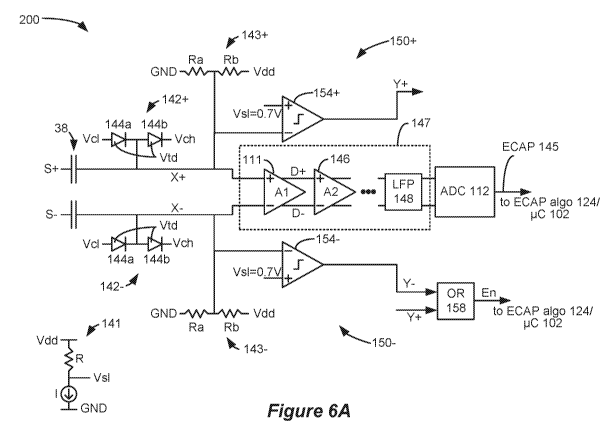
capacitors 38 and is still readily sensed by the sense amp circuit 110. In
other examples, the
ECAP may be sensed directly at the electrodes 16 without passage through
intervening
capacitors 38.
[0043] As
shown, an ECAP algorithm 124 is programmed into the control circuitry
102 to receive and analyze the digitized ECAPs. One skilled in the art will
understand that
the ECAP algorithm 124 can comprise instructions that can be stored on non-
transitory
machine-readable media, such as magnetic, optical, or solid-state memories
within the IPG
100 (e.g., stored in association with control circuitry 102).
[0044] In the
example shown in Figure 4, the ECAP algorithm 124 operates within
the IPG 100 to determine one or more ECAP features, which may include but are
not limited
to:
= a height of any peak (e.g., H N1) present in the ECAP;
= a peak-to-peak height between any two peaks (such as H PtoP from Ni to
P2);
= a ratio of peak heights (e.g., H N1 / H P2);
= a peak width of any peak (e.g., the full width half maximum of a Ni, FWHM
N1);
= an area under any peak (e.g., A N1);
= a total area (A tot) comprising the area under positive peaks with the
area under
negative peaks subtracted or added;
16
CA 03135375 2021-09-28
WO 2020/205234
PCT/US2020/023182
= a length of any portion of the curve of the ECAP (e.g., the length of the
curve from
P1 to N2, L PltoN2)
= any time defining the duration of at least a portion of the ECAP (e.g.,
the time from
P1 to N2, t PltoN2);
= a time delay from stimulation to issuance of the ECAP, which is
indicative of the
neural conduction speed of the ECAP, which can be different in different types
of
neural tissues;
= any mathematical combination or function of these variables (e.g., H N1 /
FWHM N1 would generally specify a quality factor of peak Ni).
[0045] Once the
ECAP algorithm 124 determines one or more of these features, it
may then adjust the stimulation that the IPG 100 provides, for example by
providing new data
to the stimulation circuitry 28 via bus 118. This is explained further in U.S.
Patent
Application Publications 2017/0296823 and 2019/0099602. In one simple example,
the
ECAP algorithm 124 can review the height of the ECAP (e.g., its peak-to-peak
voltage), and
in closed loop fashion adjust the amplitude I of the stimulation current to
try and maintain the
ECAP to a desired value.
[0046] Figures
5A and 5B show a percutaneous lead 15, and show the stimulation
program example of Figure 2A in which electrodes E4 and E5 are used to produce
pulses in a
bipolar mode of stimulation, with (during the first phase 30a) E4 comprising
an anode and E5
a cathode, although other electrode arrangements (e.g., tripoles, etc.) could
be used as well.
Such stimulation produces an electromagnetic (EM) field 130 in a volume of the
patient's
tissue around the selected electrodes. Some of the neural fibers within the EM
field 130 will
be recruited and fire, particularly those proximate to the cathodic electrode
E5. Hopefully the
sum of the neural fibers firing will mask signals indicative of pain in an SCS
application, thus
providing the desired therapy. The recruited neural fibers in sum produce an
ECAP, which
can travel both rostrally toward the brain and caudally away from the brain.
The ECAP
passes through the spinal cord by neural conduction with a speed which is
dependent on the
neural fibers involved in the conduction. In one example, the ECAP may move at
a speed of
about 5 cm / 1 ms.
[0047] The ECAP
is preferably sensed differentially using two electrodes, and
Figures 5A and 5B show different examples. In Figure 5A, a single electrode E8
on the lead
15 is used for sensing (S+), with another signal being used as a reference (S-
). In this
example, the sensing reference S- comprises a more distant electrode in the
electrode array 17
or (as shown) the case electrode Ec. (However, reference S- could also
comprise a fixed
17
CA 03135375 2021-09-28
WO 2020/205234
PCT/US2020/023182
voltage provided by the IPG 100, such as ground, in which case sensing would
be said to be
single-ended instead of differential). In Figure 5B, two lead-based electrodes
are used for
sensing, with such electrodes either being adjacent or at least relatively
close to one another.
Specifically, in this example, electrode E8 is again used for sensing (S+),
with adjacent
electrode E9 providing the reference (S-). This could also be flipped, with E8
providing the
reference (S-) for sensing at electrode E9 (S+). Sensing a given ECAP at
different electrodes
can allow the ECAP algorithm 124 to understand the time difference between the
arrival of
the ECAP at each of the electrodes. If the distance x between the electrodes
is known, the
ECAP algorithm 124 can then compute speed of the ECAP. As noted above, ECAP
speed is
indicative of the neural fibers involved in neural recruitment and conduction,
which can be
interesting to know in its own right, and which may be useful to the ECAP
algorithm 124 in
adjusting the stimulation provided by the stimulation circuitry 28.
[0048] Figure
5C shows waveforms for the stimulation program, as well as the signal
that would appear in the tissue at sensing electrode E8 (S+). As well as
including the ECAP
to be sensed, the signal at the sensing electrode S+ also includes a
stimulation artifact 134.
The stimulation artifact 134 comprises a voltage that is formed in the tissue
as a result of the
stimulation, i.e., as result of the EM field 130. As described in U.S. Patent
Application
Publication 2019/0299006, the PDACs and NDACs used to form the currents in the
tissue
have high output impedances. This can cause the voltage in the tissue to vary
between
ground and the compliance voltage VH used to power the DACs, which as noted
earlier can
be a high voltage (e.g., as high as 18V). The magnitude of the stimulation
artifact 134 at a
given sensing electrode S+ or its reference S- can therefore be high (e.g.,
several Volts), and
significantly higher than the magnitude of the ECAP. The magnitude of the
stimulation
artifact 134 at the sensing electrodes S+ and S- is dependent on many factors.
For example,
the stimulation artifact 134 will be larger if the sensing electrodes are
closer to the electrodes
used to provide the stimulation (E4, E5). The stimulation artifact 134 is also
generally larger
during the provision of the pulses, although it may still be present even
after the pulse (i.e.,
the last phase 30b of the pulse) has ceased due to the capacitive nature of
the tissue, which
keeps the electric field 130 from dissipating immediately.
[0049] The
relatively large-signal background stimulation artifact 134 can make
resolution and sensing of the small-signal ECAP difficult at the sense amp
circuit 110. To
ameliorate this concern, it can be beneficial to use a sensing electrode S+
that is far away
from the stimulating electrodes. See, e.g., U.S. Patent Application Serial No.
16/661,549,
filed October 23, 2019. This can be beneficial because the stimulation
artifact 134 would be
18
CA 03135375 2021-09-28
WO 2020/205234
PCT/US2020/023182
smaller at a distant sensing electrode, and because the ECAP would pass a
distant sensing
electrode at a later time when the stimulation artifact 134 might have
dissipated (e.g., ECAP2
in Fig. 5C). However, using a distant sensing electrode is not always possible
or practical.
For one, the electrode array 17 may simply not be large enough, and therefore
no electrode
may be suitably far enough away from the stimulating electrodes to ideally
operate as the
sensing electrode. Likewise, the magnitude of the ECAP also diminishes as
distance from the
stimulating electrodes increases, and therefore while the stimulation artifact
134 would be
smaller at a more distant sensing electrode, so too would the ECAP, again
making sensing
difficult.
[0050] Sensing
the ECAP may also be easier during periods when the stimulation
artifact 134 is smaller. For example, and as shown in Figure 5C, the
stimulation artifact 134
can be relatively large during the time that the pulse (i.e., its phases) is
issuing (30a and 30b),
making sensing of ECAP (e.g., ECAP1) particularly difficult during that time.
It may then be
desirable to sense the ECAP after the pulse has ceased, when the stimulation
artifact is
smaller and decreasing (e.g., ECAP2). However, sensing the ECAP after
cessation of the
pulse is not always possible, depending on various factors. For example, if
the sensing
electrode S+ is close to the stimulating electrodes, if the pulse width of the
pulse (or its
phases) is relatively long, or if the speed of the ECAP is relatively fast, it
cannot always be
possible to sense the ECAP after cessation of the pulse. Also, it may be
necessary to use
passive charge recovery after the cessation of the pulse. As noted earlier,
passive charge
recovery involves shorting the electrode nodes 39 to a reference voltage
(e.g., Vbat) through
passive charger recovery switches 41, (Fig. 3). ECAP sensing may be difficult
when the
passive charge recovery switches are closed, as the electrode node 39 carrying
the ECAP to
the sense amp circuit 110 would be shorted to the reference voltage during
this time. It may
therefore be necessary in certain circumstances to sense the ECAP during the
provision of the
pulse or one of its phases.
[0051]
Differential sensing, in which the reference electrode S- is also exposed to
the
tissue and therefore to the stimulation artifact 134 to at least some degree,
can assist ECAP
resolution, and is shown in Figure 5D. A simple example of sense amp circuit
110 is shown,
which includes a differential amplifier 111. Also shown is a simple example of
the circuitry
within the differential amplifier 111, although it should be noted that many
different
differential amplifier circuits exist and can be used as well. Understand that
the multiplexer
108 (Fig. 4) or other selector circuit could be present between the electrode
nodes 39 and the
differential amplifier 111, but this not shown in Figure 5D for simplicity.
19
CA 03135375 2021-09-28
WO 2020/205234
PCT/US2020/023182
[0052] Sensing
electrode S+ and sensing reference electrode S- are coupled through
the DC-blocking capacitors 38 (if used) to derive signals X+ and X- at the
electrode nodes 39
that are presented to the positive and negative inputs of the differential
amplifier 111. As
noted earlier, signals X+ and X- will be largely the same as S+ and S- present
at the selected
sensing electrodes, but with DC signal components removed. X+ and X- are
provided to the
gates (control terminals) of transistors M+ and M- in the differential
amplifier 111. The
drains of the transistors M+ and M- are connected to outputs D+ and D-, which
in turn are
coupled to the amplifier's power supply voltage Vdd via resistances R+ and R-.
The sources
of the transistors M+ and M- are connected to ground as the other power supply
voltage
through a common bias transistor Mb, which sets the total current Ib that, in
sum, can pass
through each of the legs (I+, I-) of the differential amplifier. Resistances
R+ and R- are equal
and are represented as simple resistors, although active devices (e.g., PMOS
transistor) could
also be used. The output of the amplifier 111, Vo, equals the difference in
the voltages at
outputs D+ and D-, which in turn is influenced by the difference in the
signals present at X+
and X-. Signals X+ and X-, if different, will turn transistors M+ and M- on to
different
degrees, thus causing different currents I+ and I- to flow through each leg.
This produces
different voltage drops across the resistances R+ and R-, and thus different
voltages at D+
and D-. In short, Vo = D+ - D- = A(X+ - X-), where A is the gain of the
amplifier.
[0053] If the
stimulation artifact 134 is present at both the sensing electrode S+ and
reference electrode S-, the differential amplifier 111 will subtract the
stimulation artifact as a
common mode voltage from the output, ideally leaving only the ECAP to be
sensed at the
output. Note that the magnitude of the stimulation artifact 134 may not be
exactly the same
at sensing electrodes S+ and S-, which is not surprising as each is
necessarily located at a
different distance from the stimulating electrodes, and so common mode removal
of the
stimulation artifact may be not be perfect. Nevertheless, differential sensing
allows the
stimulation artifact 134 to be removed to at least some degree, making it
easier to resolve the
small-signal ECAP.
[0054]
Differential sensing as illustrated in Figure 5D can however be problematic,
in
particular because of limitations inherent in the differential amplifier 111.
As noted earlier,
the stimulation artifact 134 can vary by several Volts in the tissue, and X+
and X- may
exceed the input requirements of the differential amplifier 111. Note that the
differential
amplifier 111 is powered by a power supply Vdd. This power supply Vdd is
typically on the
order of 3.3V or so, thus allowing the differential amplifier 111 to be simply
and
conveniently made from standard low voltage transistors such as M+ and M-.
While the
CA 03135375 2021-09-28
WO 2020/205234
PCT/US2020/023182
differential amplifier 111 can still work if X+ and X- are slightly higher
than Vdd, amplifier
operation would eventually be compromised if X+ and X- are significantly
higher, which is
entirely possible depending on the circumstances. Further, if X+ and X- are
too high, the
input transistors M+ and M- can become damaged, rendering the differential
amplifier 111
non-functional.
[0055] X+ and X-
can also be too low to allow for accurate sensing. In this regard,
the input transistors M+ and M- are in this example NMOS transistors which
have inherent
gate threshold voltages (e.g., Vtt=0.7V), meaning that X+ and X- at the gate
of these
transistors must be above Vtt to turn the transistors on and to produce
appreciable currents I+
and I- in each leg. If X+ or X- are lower than Vtt, I+ and I- will not flow to
a significant
degree. This means that the ECAP present in X+ may not be detected, or that
the common
mode voltage provided by the stimulation artifact 134 will not be properly
subtracted by the
differential amplifier 111.
[0056] In
short, inputs X+ and X- in the sense amp circuitry 110 should be higher
than the threshold voltages of the input transistors M+ and M-, and
(preferably) below the
differential amplifier 111's power supply voltage Vdd. Further, because X+ and
X- can be
high enough to damage the differential amplifier 111, further considerations
in the sense amp
circuit 110 are desired to ensure that this does not happen.
[0057] Figures
6A and 6B describe a first example of a sense amp circuit 200
designed to address these concerns, and includes additional circuitry to
supplement the
differential amplifier 111. As well as providing the ECAP signal to the
control circuitry
102/ECAP algorithm 124 for analysis at output 145, the sense amp circuit 200
provides one
or more enable signals (e.g., En) to inform the ECAP algorithm 124 when X+ and
X- are of a
magnitude such that the ECAP algorithm 124 can consider the ECAP at output 145
to be
valid. As explained further below, enable signal En is issued as valid when X+
and X- are of
a magnitude that is consistent with the input requirements of the differential
amplifier 111.
[0058] As a
preliminary matter, note that differential amplifier 111 may provide its
output to various processing circuits 147 prior to presentation to the control
circuitry 102 and
the ECAP algorithm 124. For example, the differential amplifier 111's
differential output
(D+ and D-) may be provided to the inputs of another differential amplifier
146, and to still
further differential amplifiers in series, etc. This can be helpful in
increasing the gain of the
detected ECAP signal, because the gains of each amplifier stage will multiply
(Al*A2, etc.).
A follower circuit or buffer could also be used in series as part of the
processing circuitry 147
between the differential amplifier 111 and the ADC 112 but such stages are not
shown.
21
CA 03135375 2021-09-28
WO 2020/205234
PCT/US2020/023182
Further, the processing circuitry 147 may include a Low Pass Filter (LPF) 148
to remove
high-frequency components in the ECAP signal that are not of interest, or that
are
inconsistent with the rate at which the ADC 112 will sample the signal. In one
example, the
LFP 148 removes frequency components of 25 kHz or higher. Processing circuitry
147 may
be considered part of the control circuitry 102.
[0059] To
prevent damage to or improper operation of the differential amplifier 111
(i.e., the first differential amplifier in series), inputs X+ and X- are
provided with clamping
circuits 142+ and 142- respectively. In the example shown, clamping circuit
142+ comprises
a serial connection of diodes 144a and 144b which are forward biased between a
low clamp
reference voltage reference (Vcl) and a high clamp reference voltage (Vch),
and with signal
X+ connected to a node between the diodes. Vcl and Vch preferably comprise
ground and
the power supply voltage Vdd (e.g., 3.3V). In this example, it is assumed that
the diodes
144a and 114b have a forward biased threshold voltage (Vtd) of 0.6V. Diode
144a would
conduct (turn on) if the voltage at X+ is less than -0.6 Volts. Because such
conductance is of
very low resistance, X+ is effectively clamped to a minimum of Vmin = -0.6
Volts. If it is
assumed that Vdd = 3.3 V, diode 144b would conduct if X+ is greater than 3.9V
Volts, which
would clamp X+ to a maximum of Vmax = 3.9V. If the voltage at X+ is at or
between -0.6
and 3.9 Volts, neither diode 144a nor 144b in clamping circuit 142+ would
conduct.
Clamping circuit 142- is similar, but connects to signal X-, and so similarly
clamps X- to a
voltage at or between -0.6 and 3.9 Volts.
[0060] To
summarize, clamping circuits 142+ and 142- allow X+ and X- to pass to
the inputs of the differential amplifier 111 without clamping if they are
between -0.6 and 3.9
Volts, but otherwise clamps voltages on these signals from exceeding 3.9 Volts
or from being
lower than -0.6V. This protects the differential amplifier 111. As noted
above, if the inputs
X+ or X- are significantly higher than the power supply voltage Vdd, the input
transistors M+
and M- may become damaged. Further, if inputs X+ or X- are too low, the
amplifier 111
may also not function properly, because the sources of drains of those
transistors M+ and M-
may start to leak to the substrate of those transistors.
[0061]
Modifications may be made to the clamping circuits 142+ and 142- to adjust
the window of permissible voltages at which clamping does not occur. For
example, Vcl and
Vch could be generated by their own generator circuits (similar to 141,
discussed below) to
produce unique values different from ground and Vdd. More than two diodes may
also be
used in series; for example, four diodes could be used in series, and if X+ or
X- is connected
between the middle two, this would expand the window to voltages from -1.2V
(ground ¨
22
CA 03135375 2021-09-28
WO 2020/205234
PCT/US2020/023182
2Vtd) to 4.5V (Vdd + 2Vtd). Zener diodes could also be used, which could break
down and
thus clamp X+ or X- at specified reverse bias voltages.
[0062] The
sense amp circuit 200 further includes DC-level shifting circuits 143+ and
143- to set signals X+ and X- to a DC voltage reference consistent with the
input
requirements for the differential amplifier 111. As discussed above, the
differential amplifier
111 can only operate reliably if signals X+ and X- are of a magnitude that
causes current I+
and I- to flow in each leg of the amplifier. In this regard, to sense the
small-signal ECAP, X+
and X- should be higher than the threshold voltage of the amplifier's input
transistors M+ and
M- (e.g., greater than Vtt = 0.7 V). It is further preferred that X+ and X-
not exceed the
power supply voltage Vdd of the differential amplifier (e.g., Vdd = 3.3V) for
proper amplifier
operation. Accordingly, signals provided to the differential amplifier 111 are
preferably
referenced with respect to a DC voltage reference within this operating range.
This reference
could comprise 1/2Vdd (e.g., 1.65 V), which comprises a midpoint between Vdd
and ground.
More preferably, the DC voltage reference could comprise 1/2(Vdd-Vtt)+Vtt
(e.g., 2.0 V), as
this value would be midpoint within the operating range 0.7V and 3.3V, and
thus allow X+
and X- to symmetrically swing +/- 1.3V from the reference while still
providing an input
magnitude suitable to operate the differential amplifier 111.
[0063] The
magnitude of the DC voltage reference can be set at signals X+ and X- via
DC-level shifting circuits 143+ and 143-. While such circuits can take
different forms, in the
example shown they comprise a resistor ladder, comprising resistors Ra and Rb
in series
biased between Vdd and ground, with signals X+ and X- connected to nodes
between the
resistors. This sets the DC voltage reference of both X+ and X- to Ra/(Ra+Rb)
* (Vdd-
ground). Thus by setting the values of Ra and Rb appropriately, the DC voltage
reference
can be set to any desired value between Vdd and ground, such as 2.0 V. AC
signals then
coupling to X+ and X- through the capacitors 38 (such as the ECAP and/or the
stimulation
artifact 134) will then be referenced to (and ride on top off) this DC voltage
reference. As a
general matter, this allows the differential amplifier 111 to be affected by
the ECAP at X+,
because the superposition of the ECAP and the DC voltage reference will cause
a change in
current I+. Preferably, Ra and Rb are large resistances, such 1 MegaOhm or
higher.
[0064] Also
present in sense amp circuitry 200 are comparator circuitries 150+ and
150-, which are connected to signals X+ and X- respectively. The goal of
comparator
circuitries 150+ and 150- are to respectively determine whether signals X+ and
X- are of a
reliable magnitude to sense ECAPs, and to indicate the same to the ECAP
algorithm 124 via
generation of an enable signal, En. Even though a DC voltage reference (e.g.,
2.0 V) is
23
CA 03135375 2021-09-28
WO 2020/205234
PCT/US2020/023182
established at X+ and X- by DC-level shifting circuits 143+ and 143-, the AC
nature of the
stimulation artifact 134 can cause large variations from this baseline. The
enable signal En
may change from time to time depending on the voltages at X+ and X-, and thus
there may be
times when the enable signal indicates to the ECAP algorithm 124 that output
145 is
providing reliable ECAP data that is valid to assess at output 145 (0'), and
times when it
indicates that output 145 is not producing reliable ECAP data and can be
ignored (1').
[0065]
Comparator circuitry 150+ includes a comparator 154+ which receives X+ at
its negative input, and a low sense reference voltage Vsl at its positive
input. In one example,
Vsl is set by a voltage generator 141 to a value that ensures that X+ is high
enough to
properly turn on transistor M+ in the differential amplifier 111. Many
different types of
generator circuits can be used to produce Vsl, including bandgap generator
circuits, but
Figure 6A shows use of a simple resistor in series with an adjustable current
source to set Vsl
to the correct value. In one example, Vsl equals (or could be slightly higher
than) the
threshold voltage of M+, i.e., Vs1=Vtt=0.7V. If X+ is higher than Vsl, the
comparator 154+
will output a '0' at signal Y+; by contrast, if X+ is lower than Vsl, the
comparator will output
a '1' at signal Y+. Comparator circuitry 150- is similar in construction and
operation to
comparator circuity 150+, and includes a comparator 154- to compare X- to Vsl
and to
determine when X- is suitably high (Y- = '0') or too low (Y- = '1').
[0066] While
signals Y+ and Y- could be sent to control circuitry 102/ECAP
algorithm 124 to operate as separate enable signals, in a preferred example,
these signals are
provided to logic circuitry such as an OR gate 158, which produces a single
enable signal,
En. Thus, if either Y+ or Y- equals '1', meaning that either X+ or X- is too
low to properly
operate the differential amplifier, En = '1'. The ECAP algorithm 124 can
therefore ignore
ECAPs reported at output 145 in this circumstance, and instead only consider
as valid ECAPs
reported when En= '0', where Y+ and Y- are both '0'. Figure 6B summarizes
operation of
the sense amp circuit 200, showing windows for X+ and X- where they are not
clamped
(between Vmax = 3.9 and Vmin = 0.6), and showing a window where they are
suitable for
sensing (greater than Vsl = 0.7). Note that the sensing window is effectively
capped at
Vmax, because V+ and V- cannot exceed this value.
[0067] Note
that the magnitude of Vsl, and perhaps operation of the comparators
154+ and 154-, could depend on the manner in which the differential amplifier
111 is built.
For example, if transistors M+ and M- in the differential amplifier 111 are
PMOS transistors,
Vsl could instead comprise a high sense reference voltage Vsh (e.g., Vdd-Vtt)
that is
provided to negative inputs of the comparators 154+ and 154-, with X+ and X-
being
24
CA 03135375 2021-09-28
WO 2020/205234
PCT/US2020/023182
provided to positive inputs of the comparators. If X+ or X- are below Vsh as
would be
necessary for proper differential amplifier 111 operation in this
circumstance, the
comparators 154+ or 154- would output a '0', and En = '0', indicating to the
ECAP algorithm
124 that ECAPs can be reliably sensed. If either of X+ or X- were above Vsh,
En = '1',
indicating the opposite.
[0068] Figures
7A and 7B describe a second example of a sense amp circuit 210.
Sense amp circuit 210 is similar to sense amp circuit 200, and includes clamp
circuits 142+
and 142- and DC-level shifting circuits 143+ and 143- as described earlier.
However, the
comparators circuitries 150+ and 150- include additional comparators 152+ and
152-
respectively. While comparators 154+ and 154- are designed to inform when X+
and X- are
too low for valid ECAP sensing, comparators 152+ and 152- are designed to
inform when X+
and X- are too high for valid ECAP sensing. In this regard, even though the
clamp circuits
142+ and 142- would clamp X+ and X- to a maximum voltage Vmax (e.g., 3.9V), it
may still
be desirable to enable ECAP sensing only if X+ and X- are below this maximum.
As noted
earlier, high values for X+ and X- can also adversely affect differential
amplifier 111
operation, even if such high values do not risk damaging the amplifier.
Furthermore, ECAP
sensing will not be reliable if X+ and X- are significantly high to cause
diodes 144b in the
clamp circuits 142+ and142- to conduct.
[0069] In this
regard, X+ and X- are sent to the positive inputs of comparators 152+
and 152-. The negative inputs are provided a high sense reference voltage Vsh.
Like Vsl,
Vsh can be set to different values (using a generator circuit like 141), but
in a preferred
example, Vsh is set to the power supply voltage Vdd (e.g., 3.3V). In this
manner,
comparators 152+ and 152- respectively output a 'I' if X+ or X- are greater
than Vsh. In
comparator circuitry 150+, the outputs of comparators 152+ and 154+ are
provided to logic
circuitry such an OR gate 156+, which outputs signal Y+. Likewise, in
comparator circuitry
150-, the outputs of comparators 152- and 154- are provided to an OR gate 156-
, which
outputs signal Y-. Signal Y+ informs whether X+ is too high (1'), too low
(1'), or suitable
for ECAP sensing (0'), and signal Y- similarly informs whether X- is too high
(1'), too low
(1'), or suitable for ECAP sensing (0'). As in circuit 200 (Fig. 6A), these
outputs Y+ and
Y- are provided to an OR gate 158 to produce the enable signal En for ECAP
sensing. Figure
7B summarizes operation of the sense amp circuit 210, showing windows for X+
and X-
where they are not clamped (between Vmax = 3.9 and Vmin = 0.6), and showing a
window
where they are suitable for sensing (between Vs1 = 0.7 and Vsh = 3.3V). The
sense amp
circuit 210 is preferred because the sensing window is smaller than and within
the window
CA 03135375 2021-09-28
WO 2020/205234
PCT/US2020/023182
where clamping does not occur. This way, ECAP sensing is disabled (En = '1')
before the
X+ or X- becomes too large or too small to be clamped by their clamp circuits
142+ and 142-
100701
Comparator circuitries 150+ and 150- need not necessarily comprise discrete
comparators such as 152+, 152-, 154+, and 154+. Instead, comparator
circuitries 150+ and
150- may include Analog-to-Digital converters (ADCs) to produce digital
representations of
X+ and X-, which may comprise discrete circuits, or which may comprise ADC
inputs of the
control circuitry 102. The digitized values for X+ and X- may then be
digitally compared
(e.g., in the control circuitry 102) to various thresholds to determine
whether they meet the
input requirements of the differential amplifier 111, e.g., to see if X+ and X-
are each
between Vs1 and Vsh. The result of these determinations can be expressed as a
digital signals
Y+ and Y- (e.g., again in the control circuitry 102), which are used by logic
circuitry (e.g.,
again in the control circuitry 102) to determine the enable signal, En. In
this regard, note that
comparator circuities 150+ and 150- may be formed, at least in part, in the
control circuitry
102 or using other digital logic circuits.
[0071] Figure 8
shows another example of a sense amp circuit 220. As with other
examples, sense amp circuit 220 includes clamp circuits 142+ and 142- to clamp
X+ and X-
to a maximum (Vmax) and preferably also minimum (Vmin) values. However, in
sense amp
circuit 220, whether ECAP sensing is indicated, and the value of enable signal
En, is set by
comparator circuitry 166 that differs compared to comparator circuitries 150+
and 150-
described earlier. Instead, in sense amp circuit 220, comparator circuitry 166
effectively
measures the current I+ and I- in each leg of the differential amplifier 111
to ensure that both
legs are producing suitable currents indicative of proper amplifier operation.
[0072] As noted
earlier, the differential amplifier 111 can only operate to sense
ECAPs if both transistors M+ and M- are on to produce significant currents I+
and I- in their
legs. In this regard, differential amplifier outputs D+ and D- may be assessed
by comparator
circuitry 166 to verify whether such currents are flowing. In the example of
differential
amplifier 111, leg currents I+ and I- flow through resistors R+ and R-, such
that D+ equals
Vdd ¨ (I+ * R+) and D- equals Vdd ¨ (I- * R-). D+ and D- are therefore lower
if significant
currents I+ and I- are flowing. If these currents are too small or
insignificant, D+ and D- will
be too high.
[0073]
Accordingly, comparator circuitry 166 can include comparators 168+ and 168-
to gauge the magnitude of differential outputs D+ and D-, which as just noted
are indicative
of the currents I+ and I- flowing through the differential amplifier's legs
and hence
26
CA 03135375 2021-09-28
WO 2020/205234
PCT/US2020/023182
compliance with the amplifier's input requirements. Comparator 168+ receives
D+ at its
positive input, while comparator 168- receives D- at its positive input. The
negative inputs of
both comparators 168+ and 168- are set to a reference voltage, Vref, by a
generator circuit
161. Again, generator circuit can take different forms, but is shown in Figure
8 as an
adjustable current in series with a resistance R. Vref is preferably just
slightly below power
supply voltage Vdd, such as 150 mV less than Vdd. These outputs Y+ and Y- can
be sent to
an OR gate 170 to produce the enable signal En that informs the ECAP algorithm
124
whether the ECAP signal present at output 145 is valid for ECAP sensing. If
both of I+ or I-
in the differential amplifier 111 are significant (because X+ and X- are
significantly high),
both of D+ or D- will be lower than Vref, and both of comparators 168+ or 168-
will output a
'0' for Y+ and Y-. OR gate 170 in turn outputs the enable signal En as a '0',
indicating that
the ECAP at output 145 is valid to sense. By contrast, if either or both of I+
or I- in the
differential amplifier 111 are too small (because either or both of X+ or X-
are too low),
either or both of D+ or D- will be higher than Vref, and either or both of
comparators 168+ or
168- will output a '1'. OR gate 170 in turn outputs the enable signal En as a
'1', indicating to
the ECAP algorithm 124 that the output 145 does not carry a valid and reliable
ECAP signal,
and hence that the output 145 should be ignored.
[0074]
Comparator circuitry 166, like 150+ and 150-, need not necessarily comprise
discrete comparators such as 168+ and 168-. Comparator circuitry 166 may
include Analog-
to-Digital converters (ADCs) to produce digital representations of D+ and D-,
which may
comprise discrete circuits, or which may comprise ADC inputs of the control
circuitry 102.
The digitized values for D+ and D- may then be digitally compared (e.g., in
the control
circuitry 102) to Vref. The result of these determinations can be expressed as
a digital signals
Y+ and Y- (e.g., again in the control circuitry 102), which are used by logic
circuitry (e.g.,
again in the control circuitry 102) as above to determine the enable signal,
En. Thus, as with
comparator circuitries 150+ and 150-, comparator circuitry 166 may be formed,
at least in
part, in the control circuitry 102 or using other digital logic circuits.
[0075] As in
other examples, the sense amp circuitry 220 may be modified depending
on the type of differential amplifier 111 that is used.
[0076] The
various examples of the sense amp circuits can also be combined in
various ways. For example, Figure 9 shows a sense amp circuit 230 that
comprises a
combination of the approaches used in sense amp circuit 210 (Fig. 7A) and
sense amp circuit
220 (Fig. 8). As in circuit 220, comparators 168+ and 168- are used as part of
comparator
circuitries 175+ and 175-, and assess the outputs D+ and D- of the
differential amplifiers 111
27
CA 03135375 2021-09-28
WO 2020/205234
PCT/US2020/023182
by comparison to Vref to inform whether inputs X+ and X- to the differential
amplifier 111
are too small to turn on both of the amplifier's legs. In this respect,
comparators 168+ and
168- essentially take the place of comparators 154+ and 154- in Figure 7A.
Comparators
152+ and 152- are used as before to assess inputs X+ and X- to ensure that
they are not too
large. The outputs of the comparators in each circuit 150+ and 150+ can again
be logically
ORed (156+ and 156-) to generate signals Y+ and Y-, with these signals in turn
being ORed
(158) to produce the enable signal, En.
[0077] When
sensing tissue signals such as ECAPs, it is preferred that the sense amp
circuits be used in a differential mode in which each input X+ and X- is
coupleable to
electrodes in contact with the patient's tissue. As noted earlier, this is
desirable to try at the
differential amplifier to subtract the stimulation artifact 134 as a common
mode voltage, thus
making it easier to sense the small-signal ECAPs.
[0078] However,
this is not strictly necessary, and the disclosed sense amp circuits
could instead be used in a single-ended mode in which one of the amplifier
inputs (e.g., X-) is
set to a reference voltage, Vamp, as shown in Figures 10A and 10B. Such
reference voltage
can be a DC voltage such as 1/2Vdd, 2.0 V, and should be high enough to turn
on input
transistor M- of the differential amplifier 111. Single-ended sensing can be
useful to sense
other signals at the electrodes, such as the stimulation artifact 134 itself
[0079] Figure
10A shows a single-ended sense amp circuit 240 which is similar to
sense amp circuit 210 (Fig. 7A) shown earlier. Because X- is set to Vamp,
comparator
circuitry 150-, clamp circuit 142- and DC-level shifting circuit 143- are
unnecessary, and thus
are not shown. In reality, these circuits may still be present in sense amp
circuit 240, but
would simply be disabled or disconnected from the circuit when Vamp is
selected (see
multiplexer 108, Fig. 4) as the reference at input X-. Notice in this example
that signal Y+
can operate as the enable signal that determines whether input X+ is valid,
and that OR gate
158 (Fig. 4) is unnecessary.
[0080] Figure
10B shows a single-ended sense amp circuit 250 which is similar to
sense amp circuit 220 (Fig. 8) shown earlier. Because X- is set to Vamp, clamp
circuit 142-
and DC-level shifting circuit 143- are unnecessary, and could be disabled or
disconnected.
Likewise, in comparator circuitry 166, comparator 168- would be unnecessary
(or
disabled/disconnected), and again signal Y+ can operate as the enable signal,
En.
[0081] As noted
earlier, an ECAP is just one example of a neural response that can be
sensed using the disclosed sense amp circuits. Not all neural responses one
might desire to
sense are a result of stimulation, and in this regard the disclosed sense amp
circuits can be
28
CA 03135375 2021-09-28
WO 2020/205234
PCT/US2020/023182
used in an implantable device that may not include stimulation circuitry 28
(Fig. 4).
Furthermore, the disclosed sense amp circuits can be used to sense other types
of signals in
the tissue beyond neural responses. For example, the sense amp circuitry could
be used to
sense other types of signals, such as those used for measuring tissue field
potentials or tissue
resistance.
29