Note: Descriptions are shown in the official language in which they were submitted.
CA 03135480 2021-09-29
WO 2020/222875 PCT/US2019/064400
SYSTEMS AND DEVICES FOR QUALITY MONITORING OF ADDITIVE
MANUFACTURING PROCESSES
BACKGROUND
[0001] The described systems and devices relate in general to quality
control and quality
assurance systems, devices, and methods for use in analyzing manufacturing
processes and more
specifically to systems and devices that utilize embedded sensors or sensor
arrays for monitoring
the quality of additive manufacturing processes and the quality of parts and
components made by
such processes.
[0002] Additive manufacturing (AM) has rapidly evolved into a valuable
and desirable
technique for making various components or parts which, at times, are
difficult or even
impossible to fabricate with conventional machining methods. Despite the
demonstrated utility
of AM, obtaining real-time feedback and data regarding an active fabrication
process and the
quality of the part or parts being made by that process has proven to be
challenging. Obtaining
such data is particularly important considering the relatively long periods of
time required to
construct complex parts. Hidden or obscured flaws occurring in an AM created
part, which can
be caused by excessive residual stresses, can result in the final part being
unusable, thereby
wasting valuable time, resources, and AM machine life. Accordingly, there is a
need for a system
and device for monitoring, in real-time, the quality of additive manufacturing
processes and the
parts and components made by such processes.
SUMMARY
[0003] The following provides a summary of certain exemplary embodiments
of the
present invention. This summary is not an extensive overview and is not
intended to identify key
or critical aspects or elements of the present invention or to delineate its
scope. However, it is to
be understood that the use of indefinite articles in the language used to
describe and claim the
present invention is not intended in any way to limit the described system.
Rather the use of "a"
or "an" should be interpreted to mean "at least one" or "one or more".
[0004] One implementation of the disclosed system provides a first system
for use in
characterizing parts made by additive manufacturing processes. This system
comprises a sensing
- 1 -
CA 03135480 2021-09-29
WO 2020/222875 PCT/US2019/064400
device having an upper surface and a lower surface; at least one channel
formed in the upper
surface of the sensing device, wherein the at least one channel is formed to a
predetermined
depth in the upper surface of the sensing device, and wherein the at least one
channel is formed
in a predetermined pattern across the upper surface of the sensing device; and
a sensor disposed
within each channel formed in the upper surface of the sensing device, wherein
each sensor is
operative to gather information relevant to an additive manufacturing process
occurring on or in
close proximity to the sensing device. The system may further comprise a
computer or data
processor connected to or in electrical communication with each sensor,
wherein the computer or
data processor further includes software for analyzing data collected by the
sensor or plurality of
sensors. The system may further comprise a cover having a predetermined
thickness, wherein the
cover encloses each sensor disposed within a channel formed in the upper
surface of the sensing
device. The cover may be adapted to be used as a substrate for additive
manufacturing processes
and the cover may be formed by depositing successive layers of metal on the
upper surface of the
sensing device. The successive layers of metal may be deposited using an
ultrasonic additive
manufacturing process. The sensing device may be aluminum, stainless steel,
nickel alloy, or
combinations thereof. The sensor may be an optical sensor; a thermocouple; a
strain gauge; a
microphone; an accelerometer; an ultrasonic non-destructive evaluation sensor;
or a magnetic
sensor.
[0005] Another implementation of the disclosed system provides a second
system for use
in characterizing parts made by additive manufacturing processes. This system
comprises a
sensing device having an upper surface and a lower surface; a plurality of
channels formed in the
upper surface of the sensing device, wherein each channel is formed to a
predetermined depth in
the upper surface of the sensing device, wherein each channel is formed in a
predetermined
pattern across the upper surface of the sensing device, and wherein the
predetermined patterns of
the channels are formed in the same orientation relative to one another or in
different orientations
relative to one another; and a sensor disposed within each channel formed in
the upper surface of
the sensing device, wherein each sensor is operative to gather information
relevant to an additive
manufacturing process occurring on or in close proximity to the sensing
device. The system may
further comprise a computer or data processor connected to or in electrical
communication with
each sensor, wherein the computer or data processor further includes software
for analyzing data
- 2 -
CA 03135480 2021-09-29
WO 2020/222875 PCT/US2019/064400
collected by the sensor or plurality of sensors. The system may further
comprise a cover having a
predeteiniined thickness, wherein the cover encloses each sensor disposed
within a channel
formed in the upper surface of the sensing device. The cover may be formed by
depositing
successive layers of metal on the upper surface of the sensing device and the
cover may be
adapted to be used as a substrate for additive manufacturing processes. The
successive layers of
metal may be deposited using an ultrasonic additive manufacturing process. The
sensing device
may be aluminum, stainless steel, nickel alloy, or combinations thereof. The
sensors may be
optical sensors, thermocouples; strain gauges; microphones; accelerometers;
ultrasonic non-
destructive evaluation sensors; magnetic sensors; or combinations thereof.
[0006] Still another implementation of the disclosed system provides a
third system for
use in characterizing parts made by additive manufacturing processes. This
system comprises a
sensing device having an upper surface and a lower surface; a plurality of
channels formed in the
upper surface of the sensing device, wherein each channel is formed to a
predetermined depth in
the upper surface of the sensing device, wherein each channel is formed in a
predetermined
pattern across the upper surface of the sensing device, and wherein the
predetermined patterns of
the channels are formed in the same orientation relative to one another or in
different orientations
relative to one another; a sensor disposed within each channel foinied in the
upper surface of the
sensing device, wherein each sensor is operative to gather information
relevant to an additive
manufacturing process occurring on or in close proximity to the sensing
device; and at least one
additional sensor not within the sensing device for further analyzing parts
made by additive
manufacturing. The system may further comprise a computer or data processor
connected to or
in electrical communication with each sensor, wherein the computer or data
processor further
includes software for analyzing data collected by the sensor or plurality of
sensors. The system
may further comprise a cover having a predetermined thickness, wherein the
cover encloses each
sensor disposed within a channel formed in the upper surface of the sensing
device. The sensors
in the sensor plate may be optical sensors, thermocouples; strain gauges;
microphones;
accelerometers; ultrasonic non-destructive evaluation sensors; magnetic
sensors; or combinations
thereof; and wherein the additional sensors are thermal cameras; optical
cameras; three-
dimensional laser scanners; or combinations thereof.
- 3 -
CA 03135480 2021-09-29
WO 2020/222875 PCT/US2019/064400
[00071 It should be appreciated that all combinations of the foregoing
concepts and
additional concepts discussed in greater detail below (provided such concepts
are not mutually
inconsistent) are contemplated as being part of the inventive subject matter
disclosed herein and
may be implemented to achieve the benefits as described herein. Additional
features and aspects
of the disclosed system, devices, and methods will become apparent to those of
ordinary skill in
the art upon reading and understanding the following detailed description of
the example
embodiments. As will be appreciated by the skilled artisan, further
implementations are possible
without departing from the scope and spirit of what is disclosed herein.
Accordingly, the
drawings and associated descriptions are to be regarded as illustrative and
not restrictive in
nature.
BRIEF DESCRIPTION OF THE DRAWINGS
[0008] The accompanying drawings, which are incorporated into and form a
part of the
specification, schematically illustrate one or more exemplary embodiments of
the invention and,
together with the general description given above and detailed description
given below, serve to
explain the principles of the invention, and wherein:
[0009] FIG. 1 provides a perspective view of an example metal build
platform or
substrate used for additive manufacturing builds, wherein the substrate is
adapted to be mounted
within an additive manufacturing system;
[0010] FIG. 2A depicts the example substrate of FIG. 1, wherein a single
channel having
a predetermined two-dimensional geometric shape has been milled into the
substrate for
receiving a sensor such as a fiber optic sensor;
[0011] FIG. 2B depicts the example substrate of FIG. 2A, wherein a fiber
optic sensor
has been placed within the channel milled into the substrate;
[00121 FIG. 2C depicts the example substrate of FIG. 2B, wherein one or
more layers of
metal have been deposited over the fiber optic sensor using an additive
manufacturing process or
other suitable technique to create a sensor plate or sensing device;
- 4 -
CA 03135480 2021-09-29
WO 2020/222875 PCT/US2019/064400
[00131 FIG. 3 provides a perspective view of another example sensor plate
or sensing
device that includes multiple fiber optic sensors mounted within the sensor
plate or sensing
device in multiple overlapping horizontal planes to create an array of sensors
within the sensor
plate or sensing device, wherein the sensors are positioned in the same
orientation (i.e.,
substantially parallel) relative to one-another;
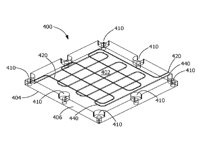
[0014] FIG. 4 provides a perspective view of another example sensor plate
or sensing
device that includes multiple fiber optic sensors mounted within the sensor
plate or sensing
device in multiple overlapping horizontal planes to create an array of sensors
within the sensor
plate or sensing device, wherein the sensors are positioned in a different
orientation (i.e.,
substantially perpendicular) relative to one-another;
[0015] FIG. 5 provides a perspective view of another example sensor plate
or sensing
device (shown without a cover); wherein multiple channels have been milled
into a substrate,
wherein a thermocouple has positioned into one channel, and wherein a foil
strain gauge has
been positioned in the other channel;
[00161 FIG. 6A provides a perspective view of another example sensor
plate or sensing
device, wherein the sensor plate or sensing device, which includes a fiber
optic sensor has been
adapted to receive a substrate or standard build plate on its upper surface to
form an assembly;
and
[0017] FIG. 6B is a top view of the assembly shown in FIG. 6A, wherein
the substrate is
positioned on top of the sensor plate or sensing device and wherein the fiber
optic sensor is
shown extending underneath a portion of the substrate for gathering data
therefrom.
DETAILED DESCRIPTION
[0018] Exemplary embodiments of the present invention are now described
with
reference to the Figures. Reference numerals are used throughout the detailed
description to refer
to the various elements and structures. Although the following detailed
description contains
many specifics for the purposes of illustration, a person of ordinary skill in
the art will appreciate
that many variations and alterations to the following details are within the
scope of the invention.
- 5 -
CA 03135480 2021-09-29
WO 2020/222875 PCT/US2019/064400
Accordingly, the following embodiments of the invention are set forth without
any loss of
generality to, and without imposing limitations upon, the claimed invention.
[0019] Various implementations provide relatively low-cost systems and
devices for
monitoring, in real-time, the quality of additive manufacturing processes and
the different parts
or components made by such processes. The sensing devices disclosed herein,
also provide
process and control capabilities that are compatible with multiple metal
additive manufacturing
(AM) platforms to enable standardization across different platforms. Example
implementations
of the disclosed sensing devices include multiple integrated sensors; reduce
overhead production
costs; enhance production repeatability; reduce fulfillment cycle times; and
enable a flexible
supply chain with part qualification data. The disclosed systems and devices
also provide
standardized process control technology that enables a flexible, affordable,
and fast response AM
supply chain.
[0020] As described herein, certain example implementations of the
disclosed sensing
devices are typically constructed using a combination of ultrasonic additive
manufacturing and
subtractive machining. As described below, a cover may be formed by depositing
successive
layers of metal on an upper surface of the sensing device. The successive
layers of metal may be
deposited in some implementations using an ultrasonic additive manufacturing
(UAM) process.
Because UAM is a solid-state process, metal can be welded over a sensor or
sensor array without
damaging embedded sensors. After an adequate amount of protective metal has
been printed over
the sensor or sensor array, the metal surface of the cover is milled flat and
the sensing device is
placed in a traditional additive manufacturing machine as the build platform.
Traditional additive
manufacturing is then performed to create a specific part or component. During
the additive
manufacturing printing process, one or more embedded sensors are used to
measure various
states and conditions of the build platform, including temperature, strain,
acceleration, and the
like. Generated data is collected and processed using various computer
hardware and software,
and the overall quality of the manufactured component or part is determined by
processing and
analyzing this data.
[0021] One example of a disclosed sensing device includes at least one
embedded fiber
optic distributed strain sensor, which may be placed, oriented, or arranged in
a variety of
- 6 -
CA 03135480 2021-09-29
WO 2020/222875 PCT/US2019/064400
predeteiinined patterns, and a temperature sensor. Thus, the embedded sensors
allow both strain
and temperature to be resolved in any direction at any point over a large
surface area. By way of
non-limiting examples, the sensor or sensors may include optical sensors;
optical fibers; and
fiber optic sensors. The sensors may also include strain gauges; foil strain
gauges; thermometers;
thermocouples; microphones; accelerometers; ultrasonic non-destructive
evaluation sensors; and
magnetic sensors. As parts are fabricated using AM on the smart baseplate,
real-time monitoring
of residual strain occurs and indicates or reveals problem areas where part
failure can occur. The
collected data can also be used to qualify the part before being placed into
service.
[0022] The sensing devices disclosed herein may be used to analyze
various additive
manufacturing processing, including by way of non-limiting examples: laser
powder bed fusion
(L-PBF); arc-DED (directed energy deposition) additive manufacturing; laser-
DED additive
manufacturing; electron beam-DED additive manufacturing; and various plastics-
based
processes. In various implementations, the internal route of the sensor fiber
utilizes a unique
curvilinear layout or configuration to capture three, two-dimensional strain
states (or more)
across the surface of the sensing device acting as a build platform. Sensor
fibers are embedded
close to the surface of printing to enhance sensitivity to surface strain
events, e.g., delamination
or cracking of L-PBF parts or components.
[0023] FIG. 1 depicts an example metal build platform used for additive
manufacturing
processes and builds, wherein the build platfoun is adapted to be mounted
directly within an
additive manufacturing system. In FIG. 1, build platform 100 includes
substrate 102; which
further includes bottom surface 104; middle portion 106; and upper surface
108. A plurality of
apertures or bolt holes 110 are formed in substrate 102 for mounting build
platform 100 within
an additive manufacturing system or apparatus for use in creating parts or
components by
additive manufacturing.
[0024] FIG. 2A depicts the example substrate of FIG. 1, wherein a single
channel having
a predetermined two-dimensional geometric shape has been milled into the
substrate for
receiving a sensor such as a fiber optic sensor. FIG. 2B depicts the example
substrate of FIG. 2A,
wherein a fiber optic sensor has been placed within the channel milled into
the substrate; and
FIG. 2C depicts the example substrate of FIG. 2B, wherein one or more layers
of metal have
- 7 -
CA 03135480 2021-09-29
WO 2020/222875 PCT/US2019/064400
been deposited over the fiber optic sensor using an additive manufacturing
process or other
suitable technique to create a sensor plate or sensing device, which may be
referred to as a
"smart baseplate". In FIGS. 2A-2C, sensing device 200 is essentially a
modified build platform
that includes substrate 202, which further includes bottom surface 204; middle
portion 206; and
upper surface 208. A plurality of apertures or bolt holes 210 are formed in
substrate 202 for
mounting sensing device 200 within an additive manufacturing system or
apparatus for use in
creating parts or components by additive manufacturing. As best shown in FIG.
2A, channel 220
is milled into upper surface 208 to a predetermined depth and in a
predetermined pattern. In this
and other implementations, the predetermined pattern may be changed or
modified based on a
specification application or use of sensing device 200. Accordingly, the
curvilinear shape of
channel 220 shown in FIG. 2A is a non-limiting example and many other shapes
and geometries
are possible. As best shown in FIG. 2A, sensor 230, which in this non-limiting
example is a fiber
optic sensor, is disposed within channel 220. Sensor 230 includes first
connector 232 and second
connector 234, which are used to connect the sensor to a computer or data
processor that
includes software for analyzing data collected by the sensor. As best shown in
FIG. 2C, sensing
device 200 includes cover 250, which is formed on upper surface 208 by
depositing successive
layers of metal thereon using, for example, an ultrasonic additive
manufacturing process. Cover
250 may then be used as the substrate for various additive manufacturing
processes, wherein
components or parts are built directly on cover 250 while information about
the components or
parts and the additive manufacturing process used to build such items is
gathered using sensing
device 200.
[0025] FIGS. 3 depicts another example sensor plate or sensing device
that includes
multiple fiber optic sensors mounted within the sensing device in multiple
overlapping horizontal
planes to create an array of sensors within the sensing device, wherein the
sensors are positioned
in the same orientation (e.g., substantially parallel) relative to one-
another. In FIG. 3, sensing
device 300 is essentially a modified build platform that includes substrate
302, which further
includes bottom surface 304; middle portion 306; and upper surface 308. A
plurality of apertures
or bolt holes 310 are formed in substrate 302 for mounting sensing device 300
within an additive
manufacturing system or apparatus for use in creating parts or components by
additive
manufacturing. First channel 320 (not visible in FIG. 3) is milled into upper
surface 308 to a
- 8 -
CA 03135480 2021-09-29
WO 2020/222875 PCT/US2019/064400
predeteimined depth and in a predetermined pattern. First sensor 330, which in
this non-limiting
example is a fiber optic sensor, is disposed within channel 320. First sensor
330 includes first
connector 332 and second connector 334, which are used to connect the sensor
to a computer or
data processor that includes software for analyzing data collected by the
sensor. Second channel
340 (not visible in FIG. 3) is milled into upper surface 308 to a
predetermined depth and in a
predetermined pattern. Second sensor 350, which in this non-limiting example
is also fiber optic
sensor, is disposed within channel 340. Second sensor 350 includes first
connector 352 and
second connector 354, which are used to connect the sensor to a computer or
data processor that
includes software for analyzing data collected by the sensor. In this and
other implementations,
the predetermined patterns may be changed or modified based on a specification
application or
use of sensing device 300. Accordingly, the curvilinear shape of channels 320
and 340 shown in
FIG. 3 is a non-limiting example and many other shapes and geometries are
possible. Sensing
device 300 includes cover 360, which may be formed on upper surface 308 by
depositing
successive layers of metal thereon using, for example, an ultrasonic additive
manufacturing
process. Cover 360 may then be used as the substrate for various additive
manufacturing
processes, wherein components or parts are built directly on cover 360 while
information about
the components or parts and the additive manufacturing process used to build
such items is
gathered using sensing device 300.
[0026] FIG. 4 depicts another example sensor plate or sensing device that
includes
multiple fiber optic sensors mounted within the sensing device in multiple
overlapping horizontal
planes to create an array of sensors within the sensing device, wherein the
sensors are positioned
in a different orientation (e.g., substantially perpendicular) relative to one-
another. In FIG. 4,
sensing device 400 is essentially a modified build platform that includes
substrate 402, which
further includes bottom surface 404; middle portion 406; and upper surface
408. A plurality of
apertures or bolt holes 410 are formed in substrate 402 for mounting sensing
device 400 within
an additive manufacturing system or apparatus for use in creating parts or
components by
additive manufacturing. First channel 420 is milled into upper surface 408 to
a predetermined
depth and in a predetermined pattern. A fiber optic sensor may be disposed
within first channel
420. Second channel 440 is milled into upper surface 408 to a predetermined
depth and in a
predetermined pattern, which is different than the pattern of first channel
420. A fiber optic
- 9 -
CA 03135480 2021-09-29
WO 2020/222875 PCT/US2019/064400
sensor may be disposed within second channel 440. As shown in FIG. 4, the
paths of channels
420 and 440 overlap, but are substantially perpendicular to one another. In
this and other
implementations, the predetermined patterns may be changed or modified based
on a
specification application or use of sensing device 400. Accordingly, the
curvilinear shape of
channels 420 and 440 shown in FIG. 4 is a non-limiting example and many other
shapes and
geometries are possible. Although not shown in FIG. 4, sensing device 400
typically includes a
cover, which may be formed on upper surface 408 by depositing successive
layers of metal
thereon using, for example, an ultrasonic additive manufacturing process. The
cover may then be
used as the substrate for various additive manufacturing processes, wherein
components or parts
are built directly on the cover while information about the components or
parts and the additive
manufacturing process used to build such items is gathered using sensing
device 400. With
regard to this implementation, separating the two fibers sensors in the Z
direction (Cartesian
coordinate system) permits resolution of moments in addition to forces in the
X-Y plane. Failure
modes for build platforms commonly occur from a bending moment created by
solidification
stresses.
[0027] FIG. 5 depicts another example sensor plate or sensing device
(shown without a
cover); wherein multiple channels have been milled into a substrate, wherein a
thermocouple has
positioned into one channel, and wherein a foil strain gauge has been
positioned in the other
channel. In FIG. 5, sensing device 500 is essentially a modified build
platform that includes
substrate 502, which further includes bottom surface 504; middle portion 506;
and upper surface
508. A plurality of apertures or bolt holes 510 are formed in substrate 502
for mounting sensing
device 500 within an additive manufacturing system or apparatus for use in
creating parts or
components by additive manufacturing. First channel 520 (not visible in FIG.
3) is milled into
upper surface 508 to a predetermined depth and in a predetermined pattern,
which in this
example is linear. First sensor 530, which in this non-limiting example is a
thermocouple, is
disposed within channel 520. First sensor 530 includes connector 532, which is
used to connect
the sensor to a computer or data processor that includes software for
analyzing data collected by
the sensor. Second channel 540 is milled into upper surface 508 to a
predetermined depth and in
a predetermined pattern. Second sensor 550, which in this non-limiting example
is a foil strain
gauge, is disposed within channel 540. Second sensor 550 includes connectors
552, which are
- 10 -
CA 03135480 2021-09-29
WO 2020/222875 PCT/US2019/064400
used to connect the sensor to a computer or data processor that includes
software for analyzing
data collected by the sensor. In this and other implementations, the
predetermined patterns may
be changed or modified based on a specification application or use of sensing
device 500.
Accordingly, the linear shape of channels 520 and 540 shown in FIG. 5 is a non-
limiting
example and many other shapes and geometries are possible. Although not shown
in FIG. 5,
sensing device 500 typically includes a cover, which may be formed on upper
surface 508 by
depositing successive layers of metal thereon using, for example, an
ultrasonic additive
manufacturing process. The cover may then be used as the substrate for various
additive
manufacturing processes, wherein components or parts are built directly on the
cover while
information about the components or parts and the additive manufacturing
process used to build
such items is gathered using sensing device 500.
[0028] FIG. 6A depicts another example sensor plate or sensing device,
wherein the
sensing device, which includes a fiber optic sensor, has been adapted to
receive a substrate or
standard build platform on its upper surface to form an assembly. FIG. 6B is a
top view of the
assembly shown in FIG. 6A, wherein the substrate is positioned on top of the
sensing device and
wherein the fiber optic sensor is shown extending underneath a portion of the
substrate for
gathering data therefrom. In FIGS. 6A-6B, sensing system 600 includes sensing
device 602
includes bottom surface 604; middle portion 606; and upper surface 608. A
plurality of apertures
or bolt holes 610 are formed in sensing device 602 for receiving bolts 690 or
other attachment
devices that connect build platform 680 to sensing device 602. Channel 620 is
milled into upper
surface 608 to a predetermined depth and in a predetermined pattern. In this
and other
implementations, the predetennined pattern may be changed or modified based on
a specification
application or use of sensing device 602. Accordingly, the curvilinear shape
of channel 620
shown in FIGS. 6A-6B is a non-limiting example and many other shapes and
geometries are
possible. Sensor 630, which in this non-limiting example is a fiber optic
sensor is disposed
within channel 620. In this implementation, a cover may or may not be formed
on upper surface
608; however, build platform 680 is mounted over at least a portion of sensor
630 and secured to
upper surface 608 as previously described. Once fabricated and assembled,
sensing system 600
may be placed within an additive manufacturing system or apparatus for normal
use.
-11-
(00291 Some implementations of the disclosed systems and device include
sensors that
are physically separate from the sensors embedded in the substrate, but that
still gather data
relevant to the quality and characteristics of a part being manufactured on
the substrate. By way
of non-limiting examples, these additional sensors may include thermal
cameras; optical
cameras; three-dimensional laser scanners; or combinations thereof that are in
electrical
communication with a computer or data processor that is also in electrical
communication with
the embedded sensors.
100301 Some implementations of the disclosed systems and devices include
sensing
devices that may be re-used, as opposed to being single-use disposable or
consumable devices. In
these implementations, a sensing device with a cover is created and then
placed in an additive
manufacturing system where a part or component is then built on sensing device
acting as a build
platform for the additive manufacturing process. Once the part or component is
created, it is
removed from the sensing device using electrical discharge machining (EMI) or
another suitable
process. A predetermined amount of material is then removed from the cover
(for example, .010-
.050 inches) to clean and prepare the cover of the sensing device for use in
creating another part
or component using additive manufacturing. In this manner, with the cover
being created to have
a suitable predetermined height, sensing devices such as those disclosed
herein may he used
multiple times rather than just once.
100311 The present invention is generally compatible with, generally
related or applicable
to, or generally relevant regarding the technologies described in the
following patent references;
U.S. Patent No. 6,685,365; U.S. Patent No. 6,443,352; US. Patent No.
6,457,629; U.S.
Patent No. 6,463,349; U.S. Patent No. 6,519,500; US. Patent No. 8,082,966;
U.S. Patent
No. 8,272,424; U.S. Patent No. 9,346,120; and U.S. Patent No. 9,446,475.
[00321
- 12 -
Date Recite/Date Received 2023-05-15
100331 As previously stated and as used herein, the singular farms "a,"
"an," and "the,"
refer to both the singular as well as plural, unless the context clearly
indicates otherwise. The
term "comprising" as used herein is synonymous with "including," "containing,"
or
"characterized by," and is inclusive or open-ended and does not exclude
additional, unrecited
elements or method steps. Although many methods and materials similar or
equivalent to those
described herein can be used, particular suitable methods and materials are
described herein,
Unless context indicates otherwise, the recitations of numerical ranges by
endpoints include all
numbers subsumed within that range. Furthermore, references to "one
implementation" are not
intended to be interpreted as excluding the existence of additional
implementations that also
incorporate the recited features. Moreover, unless explicitly stated to the
contrary,
implementations "comprising" or "having" an element or a plurality of elements
having a
particular property may include additional elements whether or not they have
that property.
100341 The terms "substantially" and "about- used throughout this
specification are used
to describe and account for small fluctuations, such as due to variations in
processing. For
example, these terms can refer to less than or equal to +5%. such as less than
or equal to +2%,
such as less than or equal to 1%, such as less than or equal to 0.5%, such
as less than or equal
to 10.2%, such as less than or equal to 10.1%, such as less than or equal to
+0.05%, and/or 0%.
190351 Underlined and/or italicized headings and subheadings are used for
convenience
only, do not limit the disclosed subject matter, and are not referred to in
connection with the
interpretation of the description of the disclosed subject matter. All
structural and functional
equivalents to the elements of the various implementations described
throughout this disclosure
that are known or later come to be known to those of ordinary skill in Ihe art
are expressly
intended to be encompassed by the disclosed subject matter. Moreover, nothing
disclosed
herein is intended to be dedicated to the public regardless of whether such
disclosure is
explicitly recited in the above description.
100361 There may be many alternate ways to implement the disclosed
inventive subject
matter. Various functions and elements described herein may be partitioned
differently from
- 13 -
Date Recite/Date Received 2023-05-15
CA 03135480 2021-09-29
WO 2020/222875 PCT/US2019/064400
those shown without departing from the scope of the disclosed inventive
subject matter. Generic
principles defined herein may be applied to other implementations. Different
numbers of a given
module or unit may be employed, a different type or types of a given module or
unit may be
employed, a given module or unit may be added, or a given module or unit may
be omitted.
[0037] It should be appreciated that all combinations of the foregoing
concepts and
additional concepts discussed in greater detail herein (provided such concepts
are not mutually
inconsistent) are contemplated as being part of the disclosed inventive
subject matter. In
particular, all combinations of claimed subject matter appearing at the end of
this disclosure are
contemplated as being part of the inventive subject matter disclosed herein.
While the disclosed
inventive subject matter has been illustrated by the description of example
embodiments and
example implementations thereof, and while the example embodiments have been
described in
certain detail, there is no intention to restrict or in any way limit the
scope of the appended
claims to such detail. Additional advantages and modifications will readily
appear to those
skilled in the art. Therefore, the invention in its broader aspects is not
limited to any of the
specific details, representative devices and methods, and/or illustrative
examples shown and
described. Accordingly, departures may be made from such details without
departing from the
spirit or scope of the general inventive concept.
- 14 -