Note: Descriptions are shown in the official language in which they were submitted.
SURFACE CODE COMPUTATIONS USING AUTO-CCZ QUANTUM STATES
BACKGROUND
[0001] This specification relates to quantum computing.
[0002] Classical computers have memories made up of bits, where each
bit can
represent either a zero or a one. Quantum computers maintain sequences of
quantum bits,
called qubits, where each quantum bit can represent a zero, one or any quantum
superposition of zeros and ones. Quantum computers operate by setting qubits
in an initial
state and controlling the qubits, e.g., according to a sequence of quantum
logic gates.
SUMMARY
[0003] This specification describes various methods, systems and
apparatus for
performing surface code computations using Auto-CCZ states.
[0004] In general, one innovative aspect of the subject matter
described in this
specification can be implemented in a method for implementing a delayed choice
CZ
operation on a first data qubit and a second data qubit using a quantum
computer, the method
comprising: preparing a first routing qubit and a second routing qubit in a
magic state;
interacting i) the first data qubit with the first routing qubit, and ii) the
second data qubit with
the second routing qubit using a first CNOT operation and a second CNOT
operation,
respectively, wherein the first data qubit and second data qubit act as a
first control and a
second control for the first CNOT operation and the second CNOT operation,
respectively;
storing the first routing qubit and second routing qubit; receiving, from a
classical processor,
a first classical bit; determining whether the first classical bit represents
an off state or an on
state; in response to determining that the first classical bit represents an
off state: applying a
first Hadamard gate to the first routing qubit and applying a second Hadamard
gate to the
second routing qubit; measuring the first routing qubit using a Z basis
measurement to obtain
a second classical bit measuring the second routing qubit using a Z basis
measurement to
obtain a third classical bit; and performing classically controlled fix up
operations on the first
data qubit and second data qubit using the second classical bit and the third
classical bit.
[0005] Other implementations of these aspects includes corresponding
computer
systems, apparatus, and computer programs recorded on one or more computer
storage
devices, each configured to perform the actions of the methods. A system of
one or more
classical and quantum computers can be configured to perform particular
operations or
actions by virtue of having software, fiiniware, hardware, or a combination
thereof installed
1
Date Regue/Date Received 2023-04-04
on the system that in operation causes or cause the system to perform the
actions. One or
more computer programs can be configured to perform particular operations or
actions by
virtue of including instructions that, when executed by data processing
apparatus, cause the
apparatus to perform the actions.
[0006] The foregoing and other implementations can each optionally
include one or
more of the following features, alone or in combination. In some
implementations
performing classically controlled fix up operations on the first data qubit
and the second data
qubit using the second classical bit and the third classical bit comprises:
applying a classically
controlled swap operation to the second classical bit and third classical bit,
wherein the first
classical bit acts as a control for the classically controlled swap operation;
and applying a first
classically controlled Z operation to the second data qubit, wherein the third
classical bit acts
as a control for the first classically controlled Z operation; and applying a
second classically
controlled Z operation to the first data qubit, wherein the second classical
bit acts as a control
for the second classically controlled Z operation.
100071 In some implementations the method further comprises, in
response to
determining that the first classical bit represents an on state: measuring the
first routing qubit
using a Z basis measurement to obtain a fourth classical bit; measuring the
second routing
qubit using a Z basis measurement to obtain a fifth classical bit; and
performing classically
controlled fix up operations on the first data qubit and second data qubit
using the obtained
fourth classical bit and fifth classical bit.
100081 In some implementations performing classically controlled fix up
operations
on the first data qubit and the second data qubit comprises: applying a
classically controlled
swap operation to the fourth classical bit and fifth classical bit, wherein
the first classical bit
acts as a control for the classically controlled swap operation; and applying
a first classically
controlled Z operation to the second data qubit, wherein the fifth classical
bit acts as a control
for the first classically controlled Z operation; and applying a second
classically controlled Z
operation to the first data qubit, wherein the fourth classical bit acts as a
control for the
second classically controlled Z operation.
[0009] In some implementations preparing a first routing qubit and a
second routing
qubit in a magic state comprises: preparing the first routing qubit in a plus
state; preparing the
second routing qubit in a plus state; and performing a CZ operation on the
first routing qubit
and the second routing qubit.
2
Date Regue/Date Received 2023-04-04
[00010] In some implementations the first classical bit comprises an
output of a
classical computation that determines whether or not a classical controlled Z
operation is to
be perfoimed on the first data qubit and second data qubit.
[00011] In general, another innovative aspect of the subject matter
described in this
specification can be implemented in a method for implementing an auto
corrected CCZ
operation on a first, second and third data qubit using a quantum computer,
the method
comprising: preparing nine routing qubits in a magic state; interacting i) the
first data qubit
with a first routing qubit using a first CNOT operation, ii) the second data
qubit with a fourth
routing qubit using a second CNOT operation, and iii) the third data qubit
with a seventh
routing qubit using a third CNOT operation, wherein the first data qubit acts
as a control for
the first CNOT operation, the second data qubit acts as a control for the
second CNOT
operation, and the third data qubit acts as a control for the third CNOT
operation; measuring
the first, fourth and seventh routing qubits to obtain a first, fourth and
seventh classical bit;
storing the second routing qubit, third routing qubit, fifth routing qubit,
sixth routing qubit,
eighth routing qubit and ninth routing qubit; determining whether the first
classical bit
represents an off state or an on state; in response to determining that the
first classical bit
represents an on state, applying a first Hadamard gate to the fifth routing
qubit and applying a
second Hadamard gate to the sixth routing qubit; measuring the fifth routing
qubit using a Z
basis measurement to obtain a fifth classical bit and measuring the sixth
routing qubit using a
Z basis measurement to obtain a sixth classical bit; determining whether the
fourth classical
bit represents an off state or an on state; in response to determining that
the fourth classical
bit represents an on state, applying a third Hadamard gate to the eighth
routing qubit and
applying a fourth Hadamard gate to the ninth routing qubit; measuring the
eighth routing
qubit using a Z basis measurement to obtain a eighth classical bit and
measuring the ninth
routing qubit using a Z basis measurement to obtain a ninth classical bit;
determining whether
the seventh classical bit represents an off state or an on state; in response
to determining that
the seventh classical bit represents an on state, applying a fifth Hadamard
gate to the second
routing qubit and applying a sixth Hadamard gate to the third routing qubit;
measuring the
second routing qubit using a Z basis measurement to obtain a second classical
bit and
measuring the third routing qubit using a Z basis measurement to obtain a
third classical bit;
and performing classically controlled fix up operations on the first, second
and third data
qubits using each of the classical bits.
[00012] Other implementations of these aspects includes corresponding
computer
systems, apparatus, and computer programs recorded on one or more computer
storage
3
Date Regue/Date Received 2023-04-04
devices, each configured to perform the actions of the methods. A system of
one or more
classical and quantum computers can be configured to perform particular
operations or
actions by virtue of having software, fitinware, hardware, or a combination
thereof installed
on the system that in operation causes or cause the system to perform the
actions. One or
more computer programs can be configured to perfoim particular operations or
actions by
virtue of including instructions that, when executed by data processing
apparatus, cause the
apparatus to perform the actions.
[00013] The foregoing and other implementations can each optionally
include one or
more of the following features, alone or in combination. In some
implementations preparing
nine routing qubits in a magic state comprises: preparing each of the nine
routing qubits in a
plus state; performing a CCZ operation on the first, fourth and seventh
routing qubits;
performing CZ operations on pairs of neighboring routing qubits.
[00014] In some implementations the method further comprises, in
response to
determining that the first classical bit represents an off state: measuring
the fifth routing qubit
using a Z basis measurement to obtain a tenth classical bit; measuring the
sixth routing qubit
using a Z basis measurement to obtain a eleventh classical bit; in response to
determining that
the fourth classical bit represents an off state: measuring the eighth routing
qubit using a Z
basis measurement to obtain a twelfth classical bit; measuring the ninth
routing qubit using a
Z basis measurement to obtain a thirteenth classical bit; in response to
determining that the
seventh classical bit represents an off state: measuring the second routing
qubit using a Z
basis measurement to obtain a fourteenth classical bit; measuring the third
routing qubit using
a Z basis measurement to obtain a fifteenth classical bit; and performing
classically
controlled fix up operations on the first, second and third data qubits using
each of the tenth-
fifteenth classical bits.
[00015] In some implementations performing classically controlled fix up
operations
on the first, second and third data qubits comprises: applying a first
classically controlled
swap operation to the second classical bit and third classical bit, wherein
the seventh classical
bit acts as a control for the first classically controlled swap operation;
applying a second
classically controlled swap operation to the fifth classical bit and sixth
classical bit, wherein
the first classical bit acts as a control for the second classically
controlled swap operation;
applying a third classically controlled swap operation to the eighth classical
bit and ninth
classical bit, wherein the fourth classical bit acts as a control for the
third classically
controlled swap operation; applying multiple classically controlled Z
operations to the first,
second, and third data qubits, wherein each classically controlled Z operation
uses one of the
4
Date Regue/Date Received 2023-04-04
second, third, fifth, sixth, eighth or ninth classical bits as a control for
the classically
controlled Z operation; applying multiple classically controlled-controlled Z
operations to the
first, second and third data qubits, wherein each classically controlled-
controlled Z operation
uses two of the first, fourth and seventh classical bits as controls for the
classically
controlled-controlled Z operation.
[00016] In some implementations applying multiple classically controlled
Z operations
to the first, second, and third data qubits, wherein each classically
controlled Z operation uses
one of the second, third, fifth, sixth, eighth or ninth classical bits as a
control for the
classically controlled Z operation, comprises: applying a first classically
controlled Z
operation to the third data qubit, wherein the second classical bit acts as a
control for the first
classically controlled Z operation; applying a second classically controlled Z
operation to the
second data qubit, wherein the third classical bit acts as a control for the
second classically
controlled Z operation; applying a third classically controlled Z operation to
the third data
qubit, wherein the fifth classical bit acts as the control for the third
classically controlled Z
operation; applying a fourth classically controlled Z operation to the first
data qubit, wherein
the sixth classical bit acts as the control for the fourth classically
controlled Z operation;
applying a fifth classically controlled Z operation to the second data qubit,
wherein the eighth
classical bit acts as the control for the fifth classically controlled Z
operation; and applying a
sixth classically controlled Z operation to the first data qubit, wherein the
ninth classical bit
acts as the control for the sixth classically controlled Z operation.
[00017] In some implementations applying multiple classically controlled-
controlled Z
operations to the first, second and third data qubits, wherein each
classically controlled-
controlled Z operation uses two of the first, fourth and seventh classical
bits as controls for
the classically controlled-controlled Z operation, comprises: applying a first
classically
controlled-controlled Z operation to the first data qubit, wherein the first
classical bit and
fourth classical bit act as controls for the first classically controlled-
controlled Z operation;
applying a second classically controlled-controlled Z operation to the second
data qubit,
wherein the fourth classical bit and seventh classical bit act as controls for
the second
classically controlled-controlled Z operation; and applying a third
classically controlled-
controlled Z operation to the third data qubit, wherein the first classical
bit and seventh
classical bit act as controls for the third classically controlled-controlled
Z operation.
[00018] In general, another innovative aspect of the subject matter
described in this
specification can be implemented in a method for producing a target state, the
method
comprising: obtaining a first number of T states of a first quality;
distilling the first number of
Date Recue/Date Received 2023-04-04
T states of the first quality into a second number of T states of a second
quality, wherein the
second number is smaller than the first number and the second quality is
higher than the first
quality; applying, using the second number of T states of the second quality,
an error
detecting operation to a tensor product of plus states to obtain the target
state, wherein the
second number of T states are provided for use in the error detecting
operation at least
partially in parallel with stabilizer measurements performed during the error
detecting
operation.
[00019] Other implementations of these aspects includes corresponding
computer
systems, apparatus, and computer programs recorded on one or more computer
storage
devices, each configured to perform the actions of the methods. A system of
one or more
classical and quantum computers can be configured to perform particular
operations or
actions by virtue of having software, firmware, hardware, or a combination
thereof installed
on the system that in operation causes or cause the system to perform the
actions. One or
more computer programs can be configured to perfoim particular operations or
actions by
virtue of including instructions that, when executed by data processing
apparatus, cause the
apparatus to perform the actions.
[00020] The foregoing and other implementations can each optionally
include one or
more of the following features, alone or in combination. In some
implementations the first
number of T states comprises at least 15 x 8 T states, and wherein the second
number of T
states comprises 8 T states.
[00021] In some implementations the target state comprises a CCZ state,
and wherein
the error detecting operation comprises a error detecting CCZ operation.
[00022] In some implementations the CCZ state is produced using a CCZ
factory of
depth 5d, where d represents error correcting code distance.
[00023] In some implementations distilling the first number of T states
of the first
quality into a second number of T states of a second quality is performed by
multiple T
factories, and wherein each T factory receives the first number of T states of
the first quality
at least partially in parallel with stabilizer measurements performed by the T
factory.
[00024] In general, another innovative aspect of the subject matter
described in this
specification can be implemented in an apparatus for performing an addition
operation, the
apparatus comprising: a register comprising a plurality of qubits, wherein the
plurality of
qubits are arranged in a two-dimensional array comprising multiple rows,
wherein each row
is associated with a value at a respective position in a sequence of n bits,
wherein the
sequence of bits represents a binary numeric value, and wherein a top row of
qubits is
6
Date Regue/Date Received 2023-04-04
associated with a value representing a most significant bit in the sequence of
n bits, and
decreasingly lower rows of qubits are associated with respective values
representing
increasingly significant bits in the sequence of n bits; and a plurality of
CCZ factories that
surround an operating area, wherein the operating area comprises an area in
which the
multiple rows of qubits are operated on to perform the addition operation, and
wherein the
CCZ factories are separated in space by gaps to allow qubits to be routed into
and through the
operating area, wherein during an addition operation, for each row of qubits
in the two-
dimensional array and starting with a row of qubits at the bottom of the two-
dimensional
array: qubits in the row are moved through one or more of the gaps and into
the operating
area where an addition operation is performed using the qubits in the row, and
after the
addition operation is performed, the qubits in the row are moved through and
out of the
operating area.
[00025] The foregoing and other implementations can each optionally
include one or
more of the following features, alone or in combination. In some
implementations the
register comprises a target register and a lookup output register that are
interleaved to allow
qubits in each register to be operated on pairwise. In some implementations,
within each
row, the qubits are interleaved to line up with the gaps.
[00026] In general, another innovative aspect of the subject matter
described in this
specification can be implemented in an apparatus for performing a lookup
operation, the
apparatus comprising: a plurality of CCZ factories that feed autoCCZ states
into a first
operating area, wherein the first operating area comprises an area in which
the lookup
operation is performed; and a lookup output register comprising plurality of
lookup output
qubits, wherein the plurality of lookup output qubits are arranged in two-
dimensional array
comprising multiple rows, wherein each row is associated with a value at a
respective
position in a sequence of n bits, wherein the sequence of bits represents a
binary numeric
value, and wherein a top row of qubits in the two-dimensional array is
associated with a value
representing a most significant bit in the sequence of n bits, and
decreasingly lower rows of
qubits in the two-dimensional array are associated with respective values
representing
decreasingly significant bits in the sequence of n bits, wherein each lookup
output qubit is
adjacent to one or more second operating areas that are positioned between
rows in the two-
dimensional array and that extend from approximately a vertical center of the
multiple rows
to one of two sides of the two-dimensional array, and wherein third operating
areas
positioned at each side of the two-dimensional array connect the second
operating areas to the
first operating area.
7
Date Recue/Date Received 2023-04-04
[00027] The foregoing and other implementations can each optionally
include one or
more of the following features, alone or in combination. In some
implementations the
apparatus further comprises a target register of qubits interleaved between
rows of lookup
output qubits, wherein the target register is idle during the lookup
operation. In some
implementations the apparatus further comprises a factor register of qubits
comprising a first
plurality of qubits that are idle and a second plurality of qubits that are
used as address bits in
the lookup operation, wherein the factor register is adjacent to the plurality
of CCZ factories
and separate from the first operating area.
[00028] The subject matter described in this specification can be
implemented in
particular ways so as to realize one or more of the following advantages.
[00029] A quantum computer implementing the presently described
techniques can
perform reaction limited computations with reduced space overhead. For
example, the
spacetime volume of CZ operations is reduced by a factor of 4 compared to
known
techniques for performing CZ operations. In addition, reaction limited
computations can be
performed with improved qubit routing ¨ qubit routing is easier due to a
decoupling of the
consumption of a CCZ state from required fixup operations needed to complete a
gate
teleportation and less routing qubits are needed.
[00030] In addition, computations that use the presently described Auto-
CCZ states
(instead of standard CCZ states) can achieve improved efficiency, since under
the Auto-CCZ
construction fixup operations are automatically performed and do not require
conditional
insertion of CZ gates based on measurements.
[00031] In addition, the presently described techniques include
efficient spacetime
hardware layouts for depth-limited circuits, e.g., ripple-carry additions, and
Clifford-limited
circuits, e.g., QROM reads. The layouts account for distillation and routing,
and are suitable
for both intermediate scale quantum computers and future quantum computers,
e.g., large-
scale superconducting qubit platforms.
[00032] The details of one or more implementations of the subject matter
of this
specification are set forth in the accompanying drawings and the description
below. Other
features, aspects, and advantages of the subject matter will become apparent
from the
description, the drawings, and the claims.
BRIEF DESCRIPTION OF THE DRAWINGS
[00033] FIG. 1 shows an example quantum computation system.
8
Date Regue/Date Received 2023-04-04
[00034] FIG. 2 is a flow diagram of an example process for performing a
delayed
choice CZ operation on a first data qubit and a second data qubit.
[00035] FIG. 3 is a circuit diagram of an example quantum circuit for
perfoiming a
delayed choice CZ operation on a first data qubit and a second data qubit.
[00036] FIG. 4 is a flow diagram of an example process for performing an
auto
corrected CCZ operation on a first, second and third data qubit.
[00037] FIG. 5 is a circuit diagram of an example quantum circuit for
performing an
auto corrected CCZ operation on a first data qubit, second data qubit and a
third data qubit.
[00038] FIG. 6 is a flow diagram of an example process for producing a
CCZ quantum
state
[00039] FIG. 7 shows an example system layout for performing a reaction
limited
ripple-carry addition operation.
[00040] FIG. 8 shows an example system layout for performing a table
lookup
operation.
[00041] Like reference numbers and designations in the various drawings
indicate like
elements.
DETAILED DESCRIPTION
Overview
[00042] Performing error corrected quantum computations involves
implementing
sequences of unitary operations and measurements, where intermediate
measurement results
are used to determine future unitary operations. For example, in the surface
code, performing
logical T and Tt gates involves a measurement dependent future S gate.
[00043] The measurement depth of a quantum circuit (defined as the
minimum number
of T gates implemented sequentially to complete execution) determines how many
times a
classical control system will: perform a set of measurements, decide which
basis to use for
the next set of measurements, and start those measurements. The speed at which
the classical
control system can run this loop, and work through the measurements,
determines the speed
of the quantum computation. The characteristic time taken for the classical
control system to
react to a measurement and perform a following dependent measurement is
referred as the
control system's "reaction time". A quantum computation whose speed is limited
by the
measurement depth of the circuit and the reaction time of the classical
control system is
referred to as a "reaction limited computation".
9
Date Regue/Date Received 2023-04-04
[00044] This specification describes techniques for decreasing the space
overhead of
reaction limited computations and improving qubit routing in reaction limited
computations.
The techniques include: an optimized reaction limited selective CZ operation,
referred to
herein as a delayed choice CZ, techniques for producing and consuming AutoCCZ
states,
which make routing easier because they decouple the consumption of the CCZ
state from the
fixup operations needed to complete a gate teleportation, an improved CCZ
distillation
factory, and apparatus for performing addition operations and lookup
operations.
Example hardware
[00045] FIG. 1 depicts an example quantum computation system 100. The
system
100 is an example of a system implemented as quantum and classical computer
programs on
one or more quantum computing devices and classical computers in one or more
locations, in
which the systems, components, and techniques described below can be
implemented.
[00046] The system 100 includes a quantum computing device 102 in data
communication with one or more classical processors 104. For convenience, the
quantum
computing device 102 and classical processors 104 are illustrated as separate
entities,
however in some implementations the classical processors 104 may be included
in the
quantum computing device 102.
[00047] The quantum computing device 102 includes components for
performing
quantum computation. For example, the quantum computing device 102 includes
quantum
circuitry 106 and control devices 108.
[00048] The quantum circuitry 106 includes components for performing
quantum
computations, e.g., components for implementing the various quantum circuits
and operations
described in this specification. For example, the quantum circuitry may
include a quantum
system that includes one or more multi-level quantum subsystems, e.g., qubits
114. The
qubits 114 are physical qubits that may be used to perform algorithmic
operations or quantum
computations. The specific realization of the one or more qubits and their
interactions may
depend on a variety of factors including the type of quantum computations that
the quantum
computing device 102 is performing. For example, the qubits may include qubits
that are
realized via atomic, molecular or solid-state quantum systems. In other
examples the qubits
may include, but are not limited to, superconducting qubits, e.g., Gmon or
Xmon qubits, or
semi-conducting qubits. Further examples of realizations of multi-level
quantum subsystems
include fluxmon qubits, silicon quantum dots or phosphorus impurity qubits. In
some cases
to the quantum circuitry may further include one or more resonators attached
to one or more
Date Regue/Date Received 2023-04-04
superconducting qubits. In some cases ion traps, photonic devices or
superconducting
cavities (with which states may be prepared without requiring qubits) may be
used.
[00049] In this specification, the term "quantum circuit" is used to
refer to a sequence
of quantum logic operations that can be applied to a qubit register to perform
a respective
computation. Quantum circuits comprising different quantum logic operations,
e.g., single
qubit gates, multi-qubit gates, etc., may be constructed using the quantum
circuitry 106.
Constructed quantum circuits can be operated/implemented using the control
devices 108.
[00050] The type of control devices 108 included in the quantum system
depend on the
type of qubits included in the quantum computing device. For example, in some
cases the
multiple qubits can be frequency tunable. That is, each qubit may have
associated operating
frequencies that can be adjusted using one or more control devices. Example
operating
frequencies include qubit idling frequencies, qubit interaction frequencies,
and qubit readout
frequencies. Different frequencies correspond to different operations that the
qubit can
perform. For example, setting the operating frequency to a corresponding
idling frequency
may put the qubit into a state where it does not strongly interact with other
qubits, and where
it may be used to perform single-qubit gates. In these examples the control
devices 108 may
include devices that control the frequencies of qubits included in the quantum
circuitry 106,
an excitation pulse generator and control lines that couple the qubits to the
excitation pulse
generator. The control devices may then cause the frequency of each qubit to
be adjusted
towards or away from a quantum gate frequency of an excitation pulse on a
corresponding
control driveline.
[00051] The control devices 108 may further include measurement devices,
e.g.,
readout resonators. Measurement results obtained via measurement devices may
be provided
to the classical processors 104 for processing and analyzing. Measurement
devices perfoun
physical measurements on properties of the qubits, either directly or
indirectly, from which
the state(s) of the qubits can be inferred. Measurement devices perform
physical
measurements on properties of the qubits, either directly or indirectly, from
which the state(s)
of the qubits can be inferred.
[00052] The quantum computing device 102 can further include one or more
quantum
state factories, e.g., T factories, that produce and store quantum states,
e.g., T or CCZ states,
to be used in computations performed by the system 100.
Programming the hardware: An example process for implementing delayed choice
CZ
operations
11
Date Regue/Date Received 2023-04-04
[00053] Known techniques for performing delayed choice CZ operations are
often not
optimal. For example, teleporting a CCZ gate produces up to three possible CZ
fixup
operations. Using known techniques based on controllable multiplexers and de-
multiplexers
to delay the choice of whether or not the various CZ fixups should be applied
would produce
eight routing qubits per potential CZ (because there are two qubits involved
in a CZ and each
must go through a multiplexer/de-multiplexer pair). The presently described
techniques is
more compact and may only use two routing qubits.
[00054] FIG. 2 is a flow diagram of an example process 200 for
performing a delayed
choice CZ operation on a first data qubit and a second data qubit. For
convenience, the
process 200 will be described as being performed by a system of one or more
classical and
quantum computing devices located in one or more locations. For example, a
quantum
computation system, e.g., the system 100 of FIG. 1, appropriately programmed
in
accordance with this specification, can perform the process 200.
[00055] The system prepares a first routing qubit and a second routing
qubit in a magic
state (step 202). For example, the system may prepare the first routing qubit
in a plus state,
prepare the second routing qubit in a plus state, and perform a CZ operation
on the first
routing qubit and the second routing qubit.
[00056] The system interacts i) the first data qubit with the first
routing qubit, and ii)
the second data qubit with the second routing qubit using a first CNOT
operation and a
second CNOT operation, respectively (step 204). The first data qubit and
second data qubit
act as a first control and a second control for the first CNOT operation and
the second CNOT
operation, respectively. Optionally, the system stores the states of the first
routing qubit and
second routing qubit.
[00057] The system receives a first classical bit from a classical
processor. In some
implementations the first classical bit may be an output of a classical
computation that
determines whether or not a classical controlled Z operation is to be
performed on the first
data qubit and second data qubit. The system determines whether the first
classical bit
represents an off state or an on state (step 206). The system determines
whether the first
classical bit represents the off state or on state by determining whether the
first classical bit is
0 (where the first classical bit represents an on state) or 1 (where the first
classical bit
represents an off state).
[00058] In response to determining that the first classical bit
represents an on state at
step 206, the system performs the below described steps 208-212. The system
applies a first
12
Date Regue/Date Received 2023-04-04
Hadamard gate to the first routing qubit and applies a second Hadamard gate to
the second
routing qubit (step 208).
[00059] The system measures the first routing qubit using a Z basis
measurement to
obtain a second classical bit and measures the second routing qubit using a Z
basis
measurement to obtain a third classical bit (step 210).
[00060] The system performs classically controlled fix up operations on
the first data
qubit and second data qubit using the second classical bit and the third
classical bit (step
212). To perfolin the classically controlled fix up operations the system:
applies a classically
controlled swap operation to the second classical bit and third classical bit,
where the first
classical bit acts as a control for the classically controlled swap operation,
applies a first
classically controlled Z operation to the second data qubit, where the third
classical bit acts as
a control for the first classically controlled Z operation, and applies a
second classically
controlled Z operation to the first data qubit, where the second classical bit
acts as a control
for the second classically controlled Z operation.
[00061] In response to determining that the first classical bit
represents an off state at
step 206, the system perfolins the below described steps 214-218. The system
measures the
first routing qubit using a Z basis measurement to obtain a fourth classical
bit (step 214). The
system measures the second routing qubit using a Z basis measurement to obtain
a fifth
classical bit (step 214). The system performs classically controlled fix up
operations on the
first data qubit and second data qubit using the obtained fourth classical bit
and fifth classical
bit (step 216).
[00062] To perform the classically controlled fix up operations on the
first data qubit
and the second data qubit, the system: applies a classically controlled swap
operation to the
fourth classical bit and fifth classical bit, where the first classical bit
acts as a control for the
classically controlled swap operation, applies a first classically controlled
Z operation to the
second data qubit, where the fifth classical bit acts as a control for the
first classically
controlled Z operation, and applies a second classically controlled Z
operation to the first data
qubit, where the fourth classical bit acts as a control for the second
classically controlled Z
operation.
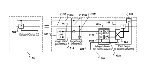
[00063] FIG. 3 is a circuit diagram of an example quantum circuit 300
for performing
a delayed choice CZ operation 308 on a first data qubit 304 and a second data
qubit 306, as
shown in box 302. The example quantum circuit 300 includes a CZ operation 310
applied to
a first routing qubit 312 and a second routing qubit 314, where both the first
routing qubit 312
13
Date Regue/Date Received 2023-04-04
and the second routing qubit 314 are prepared in a plus state. Operation 310
corresponds to
step 202 of example process 200.
[00064] The example quantum circuit 300 further includes a first CNOT
operation
316a and a second CNOT operation 316b. The first CNOT operation 316a targets
the first
routing qubit and uses the first data qubit 304 as a control. The second CNOT
operation 316b
targets the second routing qubit and uses the second data qubit 306 as a
control. Operations
316a, 316b correspond to step 204 of example process 200.
[00065] The example quantum circuit 300 further includes a first
Hadamard gate 318a
applied to the first routing qubit 312 and a second Hadamard gate 318b applied
to the second
routing qubit 314. Hadamard gates 318a and 318b are only applied when a
classical bit 320
represents an on state (i.e., when the classical bit is a 0). Operations 318a,
318b correspond
to steps 206-212 of example process 200.
[00066] The example quantum circuit 300 further includes a first
measurement
operation 322a applied to the first routing qubit 312 and a second measurement
operation
322b applied to the second routing qubit 314. Operations 322a, 322b correspond
to step 214
of example process 200.
[00067] The example quantum circuit 300 includes a classically
controlled swap
operation 324 that swaps the output of the measurement operations 322a, 322b
if the classical
bit 320 represents an on state (i.e., when the classical bit 320 is a 1). The
example quantum
circuit 300 further includes a first classically controlled Z gate 326 that is
applied to the first
data qubit 304 if an output of the classically controlled swap operation 324
corresponding to
the first routing qubit represents an on state. The example quantum circuit
300 further
includes a second classically controlled Z gate 328 that is applied to the
second data qubit
306 if an output of the classically controlled swap operation 324
corresponding to the second
routing qubit represents an on state. Operations 324-328 correspond to step
216 of example
process 200.
Programming the hardware: An example process for implementing auto corrected
CCZ
operations
[00068] Three instances of the construction for performing delayed
choice CZ
operations as described in example process 200 of FIG. 2 can be embedded
directly into a
CCZ state, so that there is one delayed choice CZ for each CZ fixup that may
be needed when
performing gate teleportation. This augments the CCZ state into an "Auto-CCZ"
state, so
called because required fixup operations are automatically performed (through
insertion of
14
Date Regue/Date Received 2023-04-04
conditional Hadamard gates within the quantum circuit where remaining Path
fixup
operations can be performed within the control-software) and do not require
conditional
insertion of CZ gates based on measurement results. This makes consuming the
state
simpler, because no corrections are needed at the consumption site.
[00069] FIG. 4 is a flow diagram of an example process 400 for
performing an auto
corrected CCZ operation on a first, second and third data qubit. For
convenience, the process
200 will be described as being performed by a system of one or more classical
and quantum
computing devices located in one or more locations. For example, a quantum
computation
system, e.g., the system 100 of FIG. 1, appropriately programmed in accordance
with this
specification, can perform the process 400.
[00070] The system prepares nine routing qubits in a magic state (step
402). For
example, the system may prepare each of the nine routing qubits in a plus
state, perform a
CCZ operation on the first, fourth and seventh routing qubits, and perform CZ
operations on
pairs of neighboring routing qubits.
[00071] The system interacts i) the first data qubit with a first
routing qubit using a
first CNOT operation, ii) the second data qubit with a fourth routing qubit
using a second
CNOT operation, and iii) the third data qubit with a seventh routing qubit
using a third
CNOT operation (step 404). The first data qubit acts as a control for the
first CNOT
operation, the second data qubit acts as a control for the second CNOT
operation, and the
third data qubit acts as a control for the third CNOT operation.
[00072] The system measures the first, fourth and seventh routing qubits
to obtain a
first, fourth and seventh classical bit (step 406).
[00073] Optionally, the system stores the second routing qubit, third
routing qubit, fifth
routing qubit, sixth routing qubit, eighth routing qubit and ninth routing
qubit.
[00074] The system determines whether the first classical bit represents
an off state or
an on state. In response to determining that the first classical bit
represents an on state, the
system applies a first Hadamard gate to the fifth routing qubit and applies a
second Hadamard
gate to the sixth routing qubit (step 408). The system measures the fifth
routing qubit using a
Z basis measurement to obtain a fifth classical bit and measures the sixth
routing qubit using
a Z basis measurement to obtain a sixth classical bit (step 410). In response
to detennining
that the first classical bit represents an off state, the system does not
perform the first
Hadmard gate or second Hadamard gate and directly performs step 410.
[00075] The system determines whether the fourth classical bit
represents an off state
or an on state. In response to determining that the fourth classical bit
represents an on state,
Date Regue/Date Received 2023-04-04
the system applies a third Hadamard gate to the eighth routing qubit and
applies a fourth
Hadamard gate to the ninth routing qubit (step 412). The system measures the
eighth routing
qubit using a Z basis measurement to obtain a eighth classical bit and
measures the ninth
routing qubit using a Z basis measurement to obtain a ninth classical bit
(step 414). In
response to determining that the fourth classical bit represents an off state,
the system does
not apply the third and fourth Hadamard gates and directly performs step 414.
1000761 The system determines whether the seventh classical bit
represents an off state
or an on state. In response to determining that the seventh classical bit
represents an on state,
the system applies a fifth Hadamard gate to the second routing qubit and
applies a sixth
Hadamard gate to the third routing qubit (step 416). The system measures the
second routing
qubit using a Z basis measurement to obtain a second classical bit and
measures the third
routing qubit using a Z basis measurement to obtain a third classical bit
(step 418). In
response to determining that the seventh classical bit represents an off
state, the system does
not apply the fifth and sixth Hadamard gates and directly performs step 418.
1000771 The system performs classically controlled fix up operations on
the first,
second and third data qubits using respective classical bits (step 420). For
example, the
system may: apply a first classically controlled swap operation to the second
classical bit and
third classical bit, where the seventh classical bit acts as a control for the
first classically
controlled swap operation, apply a second classically controlled swap
operation to the fifth
classical bit and sixth classical bit, where the first classical bit acts as a
control for the second
classically controlled swap operation, apply a third classically controlled
swap operation to
the eighth classical bit and ninth classical bit, where the fourth classical
bit acts as a control
for the third classically controlled swap operation, apply multiple
classically controlled Z
operations to the first, second, and third data qubits, where each classically
controlled Z
operation uses one of the second, third, fifth, sixth, eighth or ninth
classical bits as a control
for the classically controlled Z operation, and apply multiple classically
controlled-controlled
Z operations to the first, second and third data qubits, where each
classically controlled-
controlled Z operation uses two of the first, fourth and seventh classical
bits as controls for
the classically controlled-controlled Z operation.
1000781 Applying multiple classically controlled Z operations to the
first, second, and
third data qubits, wherein each classically controlled Z operation uses one of
the second,
third, fifth, sixth, eighth or ninth classical bits as a control for the
classically controlled Z
operation, can include: applying a first classically controlled Z operation to
the third data
qubit, wherein the second classical bit acts as a control for the first
classically controlled Z
16
Date Recue/Date Received 2023-04-04
operation; applying a second classically controlled Z operation to the second
data qubit,
wherein the third classical bit acts as a control for the second classically
controlled Z
operation; applying a third classically controlled Z operation to the third
data qubit, wherein
the fifth classical bit acts as the control for the third classically
controlled Z operation;
applying a fourth classically controlled Z operation to the first data qubit,
wherein the sixth
classical bit acts as the control for the fourth classically controlled Z
operation; applying a
fifth classically controlled Z operation to the second data qubit, wherein the
eighth classical
bit acts as the control for the fifth classically controlled Z operation; and
applying a sixth
classically controlled Z operation to the first data qubit, wherein the ninth
classical bit acts as
the control for the sixth classically controlled Z operation.
[00079] Applying multiple classically controlled-controlled Z operations
to the first,
second and third data qubits, wherein each classically controlled-controlled Z
operation uses
two of the first, fourth and seventh classical bits as controls for the
classically controlled-
controlled Z operation, can include: applying a first classically controlled-
controlled Z
operation to the first data qubit, wherein the first classical bit and fourth
classical bit act as
controls for the first classically controlled-controlled Z operation; applying
a second
classically controlled-controlled Z operation to the second data qubit,
wherein the fourth
classical bit and seventh classical bit act as controls for the second
classically controlled-
controlled Z operation; and applying a third classically controlled-controlled
Z operation to
the third data qubit, wherein the first classical bit and seventh classical
bit act as controls for
the third classically controlled-controlled Z operation.
[00080] FIG. 5 is a circuit diagram of an example quantum circuit 500
for performing
an auto corrected CCZ operation 502 on a first data qubit 504, second data
qubit 506 and a
third data qubit 508. The example quantum circuit 500 includes a CCZ operation
512 applied
to a first, fourth and seventh routing qubit in a register 510 that includes
nine routing qubits,
where each routing qubit is prepared in a plus state. The example quantum
circuit 500 further
includes multiple CZ operations, e.g., CZ operation 514, applied to pairs of
neighboring
routing qubits (with the convention that the last routing qubit neighbors the
first routing
qubit). For example, the example quantum circuit 300 includes a first CZ
operation applied
to the first and second routing qubits, a second CZ operation applied to the
second and third
routing qubits, etc. In total the example quantum circuit 500 includes nine CZ
operations.
The CCZ operation 512 and multiple CZ operation, e.g., CZ operation 514,
correspond to
step 402 of example process 400.
17
Date Regue/Date Received 2023-04-04
[00081] The example quantum circuit 500 includes three CNOT operations,
e.g.,
CNOT operation 516. A first CNOT operation targets the first routing qubit and
uses the first
data qubit as a control. A second CNOT operation targets the fourth routing
qubit and uses
the second data qubit as a control. A third CNOT operation targets the seventh
routing qubit
and uses the third data qubit as a control. The three CNOT operations
correspond to step 404
of example process 400.
[00082] The example quantum circuit 500 includes three measurement
operations, e.g.,
measurement operation 518. A first measurement operation measures the first
routing qubit.
A second measurement operation measures the fourth routing qubit. A third
measurement
operation measures the seventh routing qubit. The three measurement operations
correspond
to step 406 of example process 400.
[00083] The example quantum circuit 500 includes multiple Hadamard
gates, e.g.,
Hadamard gate 520. A first Hadamard gate and a second Hadamard gate are
applied to the
second routing qubit and third routing qubit, respectively, if a measurement
result of the
measurement operation performed on the seventh routing qubit represents an on
state. A
third Hadamard gate and a fourth Hadamard gate are applied to the fifth
routing qubit and
sixth routing qubit, respectively, if a measurement result of the measurement
operation
performed on the first routing qubit represents an on state. A fifth Hadamard
gate and a sixth
Hadamard gate are applied to the eighth routing qubit and ninth routing qubit,
respectively, if
a measurement result of the measurement operation performed on the fourth
routing qubit
represents an on state. The example quantum circuit 500 includes multiple
measurement
operations, e.g., measurement operation 522, that are applied to the second,
third, fifth, sixth,
eighth and ninth routing qubits. The Hadamard gates and measurement operations
described
correspond to steps 410-426 of example process 400.
[00084] The example quantum circuit 500 includes multiple classically
controlled
swap operations, e.g., classically controlled swap operation 524, that swap
outputs of
respective measurement operations if a respective classical bit represents an
on state. For
example, classically controlled swap operation 524 swaps the outputs of the
measurement
operations performed on the eighth and ninth routing qubits if the output of
the measurement
operation performed on the fourth routing qubit represents an on state. A
second classically
controlled swap operation swaps the outputs of the measurement operations
performed on the
fifth and sixth routing qubits if the output of the measurement operation
performed on the
first routing qubit represents an on state. A third classically controlled
swap operation swaps
the outputs of the measurement operations performed on the second and third
routing qubits
18
Date Regue/Date Received 2023-04-04
if the output of the measurement operation performed on the seventh routing
qubit represents
an on state. The classically control swap operations described correspond to
step 428 of
example process 400.
[00085] The example quantum circuit 500 includes multiple classically
controlled Z
gates, e.g., classically controlled Z gate 526, that are applied to the first
data qubit 504,
second data qubit 506 and third data qubit 508 based on outputs of the three
classically
controlled swap operations. For example, a first Z gate is applied to the
first data qubit 504 if
an output of the third classically controlled swap operation corresponding to
the second
routing qubit represents an on state. A second Z gate is applied to the second
data qubit 506
if an output of the third classically controlled swap operation corresponding
to the third
routing qubit represents an on state. A third Z gate 526 is applied to the
second data qubit
506 if an output of the second classically controlled swap operation
corresponding to the fifth
routing qubit represents an on state. A fourth Z gate is applied to the third
data qubit 508 if
an output of the second classically controlled swap operation corresponding to
the sixth
routing qubit represents an on state. A fifth Z gate is applied to the third
data qubit 508 if an
output of the first classically controlled swap operation 524 corresponding to
the eighth
routing qubit represents an on state. A sixth Z gate is applied to the first
data qubit 504 if an
output of the first classically controlled swap operation 524 corresponding to
the ninth
routing qubit represents an on state.
[00086] A seventh Z gate is applied to the third data qubit if the
output of the
measurement of the first routing qubit and the fourth routing qubit both
represent on states.
An eighth Z gate is applied to the first data qubit if the output of the
measurement of the
seventh routing qubit and the fourth routing qubit both represent on states. A
ninth Z gate is
applied to the second data qubit if the output of the measurement of the first
routing qubit and
the seventh routing qubit both represent on states. The multiple classically
controlled Z gates
correspond to step 428 of example process 400.
Programming the hardware: An example process for CCZ quantum state
distillation
[00087] Operations that are not native to the surface code can be
performed using
magic state distillation and gate teleportation. A particularly useful magic
state is the CCZ
state
ICCZ) = CCZI+r 3 = (-1)abc I abc)
a,b,cE{0,1)
19
Date Regue/Date Received 2023-04-04
This quantum state is particularly useful because the quantum equivalent of
the AND gate ¨
the Toffoli gate ¨ is not native to the surface code but can be performed by
consuming one
CCZ state. Algorithms with a lot of arithmetic, such as Grover's algorithm and
Shor's
algorithm, perform many Toffoli gates and benefit from using a state
specialized to this task.
[00088] FIG. 6 is a flow diagram of an example process 600 for producing
a CCZ
quantum state. For convenience, the process 600 will be described as being
performed by a
system of one or more classical and quantum computing devices located in one
or more
locations. For example, a quantum computation system, e.g., the system 100 of
FIG. 1,
appropriately programmed in accordance with this specification, can perform
the process
600.
[00089] The system obtains a first number of T states of a first quality
(step 602). The
system can obtain the first number of T states from a level-0 T state factory.
In some
implementations the system can perform state injection techniques to obtain
the first number
of T states.
[00090] The system distills the first number of T states of the first
quality into a second
number of T states of a second quality (step 604). The second number is
smaller than the
first number and the second quality is higher than the first quality. For
example, in some
implementations the system can implement the Reed-Muller code to distill the
first number of
T states into the second number of T states. The first number of T states can
include at least
15 x 8 T states and the second number of T states can include 8 T states. The
system can
distill the first number of T states into a second number of T states using a
level-1 T state
factory.
[00091] In some implementations the system distills the first number of
T states of the
first quality into a second number of T states of a second quality using
multiple T factories,
where each T factory receives the first number of T states of the first
quality at least partially
in parallel with stabilizer measurements performed by the T factory.
[00092] The system applies, using the second number of T states of the
second quality,
an error detecting Toffoli operation to a tensor product of plus states to
obtain the CCZ
quantum state (step 606). The second number of T states can be provided for
use in the error
detecting operation at least partially in parallel with stabilizer
measurements performed
during the error detecting operation. The system can obtain the CCZ quantum
state using a
CCZ factory that includes six level-1 T factories. In some implementations the
CCZ
Date Regue/Date Received 2023-04-04
quantum state can be obtained using a CCZ factory of depth 5d, where d
represents error
correcting code distance.
[00093] In some implementations the system chooses error correcting code
distances
for factories producing the first number of T states, second number of T
states and CCZ state
based on a target error rate and not based on layout considerations. For
example, the
probability of logical error in a single layer of surface code circuitry
covering d x d data
qubits with a characteristic physical gate error rate p is approximately pi, =
0.1(100p)((d+1)/2). A typical state distillation structure can involve on the
order of 1000 of
such patches. If the target probability of logical failure from the
distillation structure is no
more than 10-11, this would set a minimum code distance via 10-11 > 1000 *
(d+1)
0.1(100p)l 2 ) . If p = 0.001, which is a typical target physical gate error
rate, this would
(d+1\
reduce to 10-11 > 100 * 0.1k 2 ), implying a minimum code distance of 27.
[00094] The production rate of the CCZ factory can be limited by either
the level 1 or
level 2 distances. At level 2 the production rate of the factory is limited by
the factory's depth
times the cycle time times the level 2 code distance. So, under the assumption
of: a reaction
time of 10 microseconds, a cycle time of 1 microsecond, a level 1 code
distance of 17 and a
level 2 code distance of 27, the level 2 part of the factory is technically
capable of producing
states at a rate of (5.11us 27)-1 ==== 7.4 kHz. The level 1 part of the
factory needs to produce 8
level 1 T states for each CCZ state that will be output. There are six level 1
T factories, and
they have a depth of 5.75d1, which means the output rate of the entire factory
cannot be larger
than (5.75 = 17 = 1,us = 8/6)-1 ==== 7.7 kHz. Therefore the level 2 code
distance is the limiting
factor, and the factory runs at 7.4 kHz.
[00095] In a reaction limited computation, one CCZ state will be needed
per reaction
time of the classical control system. That is to say, CCZ states are consumed
at a rate of 100
kHz. Therefore, given the above assumptions, a reaction limited computation
may require
[100/7.41=14 CCZ factories running in parallel.
Example hardware layout: improved system layout for performing reaction
limited addition
operations
[00096] The above described Auto-CCZ states can be used to construct an
improved
system layout for performing reaction limited addition operations, e.g.,
implementing a
quantum ripple-carry addition circuit as described in "A new quantum ripple-
carry addition
circuit," Cuccaro et. al., arXiv preprint quant-ph/0410184, 2004. These
quantum ripple-carry
21
Date Regue/Date Received 2023-04-04
addition circuits compute the sum of two n-bit numbers a = aoai a,_i and b =
bobi where ao, 1)0 represent the lowest order bits. A, B1 represent
memory locations
where a, b1 are initially stored respectively. The numbers a and b are added
in place, and at
the end Bi contains si, the i-th bit of the sum, replacing bi. There is one
additional output
location for the high bit sn. The carry string for the addition can be defined
recursively -
co = 0 and ci+i = MAJ (a1, b1, c1) for i 1 where MAJ represents an "in place
Majority"
operation defined by MAJ (a1, b1, c) = aibi(Daici' bici such that ci = ai
ebieci for all i <
n and sn. = cn. Each ci can be computed in order, from c1 to cn. To perform an
addition of
two n-bit numbers a sequence of n MAJ gates is performed. After performing the
ladder of
MAJ gates a sequence of "UnMajority and Add" (UMA) gates is performed,
proceeding in
reverse order. Each LIMA gate uncomputes a corresponding MAJ gate and performs
a three-
way 712 addition aiefbieci.
[00097] The system layout enables some operations of the addition
circuit to be laid
out in a space-like fashion, so that they can be performed approximately
simultaneously (e.g.,
within limits of the available hardware). This is achieved by implementations
of the addition
circuit's in-place majority MAJ operations and UnMajority and Add UMA
operations that
accept CCZ states and propagate involved bits horizontally across space,
instead of vertically
through time. The entire addition circuit is not laid out in a spacelike
fashion, since this
would require a number of CCZ factories that is proportional to the size of
the addition
instead of proportional to the reaction time of the control system. Instead,
the addition is
performed back and forth across space, performing an amount of carry rippling
that keeps the
CCZ factories and corresponding classical control system operating at a system-
specific
optimal rate.
[00098] The system layout also enables CCZ states produced by CCZ
factories to be
efficiently routed into the addition operation. Each "in-place majority"
operation has four
inputs and three outputs. One of the inputs, and also one of the outputs, is a
carry qubit.
Another two of the inputs (and outputs) are data qubits - one from the target
register and one
from the offset register. The remaining input is the three qubits making up
the CCZ part of
an Auto-CCZ state. These input and output qubits must be routed in a way that
causes them
to intersect the "in-place majority" operation at the right place and at the
right time. The
presently described system layout achieves this by moving the carry qubit back
and forth
along the X axis (right/left through space), while running data qubits through
along the Y axis
(forward/back through space). CCZ factories are placed in front of and behind
the area in
22
Date Regue/Date Received 2023-04-04
which the carry qubit is moved back and forth (referred to herein an operating
area), so that
their outputs are produced directly adjacent to where they are needed making
routing trivial.
Gaps are left between adjacent factories, so that data qubits from outside the
operating area
can be routed through those gaps as needed.
[00099] As more and more data qubits are routed from behind the
operating area to in
front (or vice versa), the operating area is shifted backward (or forward).
The two data
registers are interleaved into alternating rows, so that qubits that need to
reach the same "in-
place majority" operation at the same time are adjacent. Within each row there
is additional
interleaving, spacing out qubits that are sequential in the register. This
prevents congestion
as the data qubits are routed through the gaps between the factories.
[mono] FIG. 7 shows an example system layout 700 for performing a
reaction limited
ripple-carry addition operation. The example system layout 700 is shown from
above. That
is, the horizontal axis and vertical axis are spatial axes. For example, the
example system
layout 700 can be part of a quantum chip or tiled array of chips. In the
example system
layout 700, a level 2 code distance of 27 and a level 1 code distance of 17
are assumed.
[000101] The example system includes multiple qubits. The multiple qubits
are
arranged in the example system layout 700 in a two dimensional array that
includes multiple
rows 702, where each row includes multiple qubits, e.g., 113 logical qubits.
The multiple
qubits include qubits from a lookup output register, e.g., qubits in row 702a,
and from a target
register, e.g., qubits in row 702b. Rows of qubits from the lookup output
register and rows of
qubits from the target register are interleaved to allow qubits in each
register to be operated
on pairwise, as described above.
[000102] Each row is associated with a value at a respective position in
a sequence of n
bits, where the sequence of bits represents a binary numeric value. The top
row of qubits in
the multiple rows is associated with a value representing a most significant
bit in the
sequence of n bits, and increasingly lower rows of qubits in the multiple rows
are associated
with respective values representing decreasing significant bits in the
sequence of n bits.
[000103] Rows of qubits from the target register represent the n-bit
numbers that are to
be added, where alternate qubits in each row of qubits from the target
register represent the
respective numbers to be added_ For example, when adding the number
123123123123 to
456456456456 (which for illustrative purposes only are given in decimals, not
binary), the
target register may store 142536142536142536142536. If the two-dimensional
array of
qubits has length 6 (e.g., the rows 702 include 6 qubits) then the rows 702
would include four
rows of qubits from the target register:
23
Date Regue/Date Received 2023-04-04
142536
142536
142536
142536
(where interleaving rows of qubits from the lookup register are not included
in the example).
[000104] The example system layer 700 further includes multiple CCZ
factories 704,
e.g., CCZ factory 704a, that produce the presently described Auto-CCZ states
and provide
produced states for use in the addition operation performed in the operating
area 710, e.g., for
use in "in-place majority" operations. Each CCZ factory includes two CCZ fixup
areas, e.g.,
area 714, because routing qubits emerging from a CCZ fixup box can extend
vertically into a
next layer before the control system determines how to measure the routing
qubits.
[000105] In the example system layout 700, the multiple CCZ factories 704
surround an
operating area 710. The operating area 710 is an area in which the multiple
rows of qubits
are operated on to perform the addition operation. The CCZ factories 704 are
separated in
space by gaps, e.g., gap 712, to allow qubits to be routed into and through
the operating area
710, as described above.
[000106] During an addition operation, for each row of qubits in the
multiple rows and
starting with a row of qubits at the bottom of the multiple rows: qubits in
the row are moved
through one or more of the gaps and into the operating area where an addition
operation is
performed using the qubits in the row, and after the addition operation is
performed, the
qubits in the row are moved through and out of the operating area. For
example, continuing
the example given above where 456456456456 is to be added to 123123123123 and
the
target register initially stores the number 142536142536142536142536 in four
rows of six
qubits:
142536
142536
142536
142536
the addition operation proceeds by adding the lower right 3+6 and storing the
result in qubits
below the operating area 710 and the lower row of CCZ factories. Since one
number is added
to the other at each respective position, in this example and after processing
an entire row, the
state of the machine could be:
142536
24
Date Regue/Date Received 2023-04-04
142536
142536
CCZ Factories
Operating area
CCZ Factories
547596
The addition continues scanning across each row of target qubits.
[000107] The output of the ripple carry operation can be obtained by
measuring the
qubits that have been moved through and out of the operating area.
[000108] The example system layout 700 can perform ripple-carry addition
operations
at the reaction limited rate, propagating carry information from qubit to
qubit at 100kHz.
Under reasonable physical assumptions, it is estimated that the layout would
add a pair of
thousand-qubit registers in approximately 20 milliseconds.
Example hardware layout: improved system layout for performing table lookup
operations
[000109] The above described ripple-carry addition operation is ideal for
reaction
limited computation because it has only a small amount of Clifford operations
per Toffoli
operation. A table lookup operation (also called a QROM read) is different -
for each Toffoli
operation performed in a table lookup, there multiple Clifford operations to
perform. In
particular, each Toffoli triggers a large multi-target CNOT operation that
potentially involves
all lookup output qubits. Because of this, the limiting factor during a table
lookup is not the
classical control system's reaction time but rather access to the output
qubits.
[000110] In order to target a logical qubit with a CNOT, an unused
logical-qubit sized
patch of surface code adjacent to that logical qubit is needed. The CNOT
operation will then
use that patch for d cycles, where d is the code distance. For qubits where
only one side is
accessible, only one CNOT can be performed per d cycles. Under the assumption
that a
surface code cycle time equals 1 microsecond, and using a code distance of 27
(as an
example), this suggests a maximum CNOT rate of 37kHz (instead of the 100kHz of
a
reaction limited computation).
[000111] It can be possible to work around this CNOT rate limitation. For
example, if
there are multiple single-control single-target CNOTs all targeting the same
qubit, it is
possible to fuse the many CNOTs into a single generalized CNOT where the
control is a
Pauli product of all the individual controls. However, this does not work in
the case of table
Date Regue/Date Received 2023-04-04
lookups because the set of relevant control qubits differs from output qubit
to output qubit.
Therefore, to overcome the CNOT rate limitation the presently described
example system
layout makes two sides of each qubit accessible, instead of just one. The
large multi-target
CNOT operations can then alternate between using one side, and using the other
side. This
doubles the achievable Toffoli rate from 37kHz to 74kHz, which is much closer
to 100kHz.
[000112] In addition, while performing the lookup, the example system
layout includes
a tiled row interleaving pattern of RLL R where an L represents a lookup data
row, R
represents an existing data row not involved in the lookup, and an underscore
represents an
empty access row that can be used when performing the multi-target CNOTs. The
multi-
target CNOT operations alternate between using the single inner access row and
both of the
outer access rows. In order to access the access rows, cross-row access
corridors are included
on opposing sides of the layout. The multi-target CNOT operations can
alternate between
using the two access corridors, so that they can branch into individual access
rows as needed.
[000113] FIG. 8 shows an example system layout 800 for performing a table
lookup
operation. The example system layout 800 is shown from above. That is, the
horizontal axis
and vertical axis are spatial axes. For example, the example system layout 800
can be part of
a quantum chip or tiled array of chips. In the example system layout 800, a
level 2 code
distance of 27 and a level 1 code distance of 17 are assumed.
[000114] The example system layout 800 includes multiple CCZ factories,
e.g., CCZ
factory 802, that feed the presently described auto-CCZ states into a first
operating area 804
where the lookup operation is performed. Because the first operating area 804
is positioned
centrally in the example system layout 800, it is referred to herein as a
central operating area
804.
[000115] The example system includes a lookup output register that, in
turn, includes
multiple lookup output qubits. In the example system layout 800 the multiple
lookup output
qubits are arranged in a two-dimensional array that includes multiple rows,
e.g., row 806,
where each row is associated with a value at a respective position in a
sequence of n bits that
represents a binary numeric value. A top row of qubits in the two-dimensional
array is
associated with a value representing a most significant bit in the sequence of
n bits, and
increasingly lower rows of qubits are associated with respective values
representing
decreasing significant bits in the sequence of n bits. The example system
further includes a
target register of qubits that are also arranged in rows, e.g., row 808, that
are interleaved
between rows of lookup output qubits. The target register is idle during the
lookup operation.
26
Date Regue/Date Received 2023-04-04
[000116] Each lookup output qubit is adjacent to one or more second
operating areas,
e.g., area 810, that are positioned between rows in the multiple rows and that
extend from
approximately a vertical center of the two-dimensional array of qubits to one
of two sides of
the array, e.g., side 812, and where third operating areas positioned at each
side of the two-
dimensional array connect the second operating areas to the first operating
area 804. Because
the second operating areas extend along the x axis, they are referred to
herein as horizontal
operating areas or horizontal access rows. Similarly, because the third
operating areas extend
along the y axis, they are referred to herein as vertical operating areas or
vertical access
corridors. The vertical access corridors and horizontal access rows provide
two distinct ways
to simultaneously access all output qubits when performing many-target CNOTs.
[000117] In some implementations the example system layout 800 further
includes a
factor register of qubits including a first number of qubits that are idle and
a second
number of qubits that are used as address bits in the lookup operation, where
the factor
register is adjacent to the CCZ factories and separate from the central
operating area 804.
[000118] Implementations of the digital and/or quantum subject matter and
the
digital functional operations and quantum operations described in this
specification and
appendix can be implemented in digital electronic circuitry, suitable quantum
circuitry or,
more generally, quantum computational systems, in tangibly-embodied digital
and/or
quantum computer software or firmware, in digital and/or quantum computer
hardware,
including the structures disclosed in this specification and their structural
equivalents, or in
combinations of one or more of them. The term "quantum computational systems"
may
include, but is not limited to, quantum computers, quantum information
processing
systems, quantum cryptography systems, or quantum simulators. Quantum
computation
systems in general and quantum computers specifically may be realized or based
on
different quantum computational models and architectures. For example, the
quantum
computation system may be based on or described by models such as the quantum
circuit
model, one-way quantum computation, adiabatic quantum computation, holonomic
quantum computation, analog quantum computation, digital quantum computation,
or
topological quantum computation.
[000119] Implementations of the digital and/or quantum subject matter
described in
this specification can be implemented as one or more digital and/or quantum
computer
programs, i.e., one or more modules of digital and/or quantum computer program
instructions encoded on a tangible non-transitory storage medium for execution
by, or to
27
Date Regue/Date Received 2023-04-04
control the operation of, data processing apparatus. The digital and/or
quantum computer
storage medium can be a machine-readable storage device, a machine-readable
storage
substrate, a random or serial access memory device, one or more qubits, or a
combination
of one or more of them. Alternatively or in addition, the program instructions
can be
encoded on an artificially-generated propagated signal that is capable of
encoding digital
and/or quantum information, e.g., a machine-generated electrical, optical, or
electromagnetic signal, that is generated to encode digital and/or quantum
information for
transmission to suitable receiver apparatus for execution by a data processing
apparatus.
[000120] The terms quantum information and quantum data refer to
information or
data that is carried by, held or stored in quantum systems, where the smallest
non-trivial
system is a qubit, i.e., a system that defines the unit of quantum
information. It is
understood that the term "qubit" encompasses all quantum systems that may be
suitably
approximated as a two-level system in the corresponding context. Such quantum
systems
may include multi-level systems, e.g., with two or more levels. By way of
example, such
systems can include atoms, electrons, photons, ions or superconducting qubits.
In many
implementations the computational basis states are identified with the ground
and first
excited states, however it is understood that other setups where the
computational states
are identified with higher level excited states are possible.
[000121] The teini "data processing apparatus" refers to digital and/or
quantum data
processing hardware and encompasses all kinds of apparatus, devices, and
machines for
processing digital and/or quantum data, including by way of example a
programmable
digital processor, a programmable quantum processor, a digital computer, a
quantum
computer, multiple digital and quantum processors or computers, and
combinations
thereof. The apparatus can also be, or further include, special purpose logic
circuitry, e.g.,
an FPGA (field programmable gate array), an ASIC (application-specific
integrated
circuit), or a quantum simulator, i.e., a quantum data processing apparatus
that is designed
to simulate or produce information about a specific quantum system_ In
particular, a
quantum simulator is a special purpose quantum computer that does not have the
capability to perform universal quantum computation. The apparatus can
optionally
include, in addition to hardware, code that creates an execution environment
for digital
and/or quantum computer programs, e.g., code that constitutes processor
firmware, a
protocol stack, a database management system, an operating system, or a
combination of
one or more of them.
28
Date Regue/Date Received 2023-04-04
[000122] A digital computer program, which may also be referred to or
described as
a program, software, a software application, a module, a software module, a
script, or
code, can be written in any form of programming language, including compiled
or
interpreted languages, or declarative or procedural languages, and it can be
deployed in
any form, including as a stand-alone program or as a module, component,
subroutine, or
other unit suitable for use in a digital computing environment. A quantum
computer
program, which may also be referred to or described as a program, software, a
software
application, a module, a software module, a script, or code, can be written in
any folin of
programming language, including compiled or interpreted languages, or
declarative or
procedural languages, and translated into a suitable quantum programming
language, or
can be written in a quantum programming language, e.g., QCL or Quipper.
[000123] A digital and/or quantum computer program may, but need not,
correspond
to a file in a file system. A program can be stored in a portion of a file
that holds other
programs or data, e.g., one or more scripts stored in a markup language
document, in a
single file dedicated to the program in question, or in multiple coordinated
files, e.g., files
that store one or more modules, sub-programs, or portions of code. A digital
and/or
quantum computer program can be deployed to be executed on one digital or one
quantum
computer or on multiple digital and/or quantum computers that are located at
one site or
distributed across multiple sites and interconnected by a digital and/or
quantum data
communication network. A quantum data communication network is understood to
be a
network that may transmit quantum data using quantum systems, e.g. qubits.
Generally, a
digital data communication network cannot transmit quantum data, however a
quantum
data communication network may transmit both quantum data and digital data.
[000124] The processes and logic flows described in this specification
can be
performed by one or more programmable digital and/or quantum computers,
operating
with one or more digital and/or quantum processors, as appropriate, executing
one or more
digital and/or quantum computer programs to perfoun functions by operating on
input
digital and quantum data and generating output. The processes and logic flows
can also be
performed by, and apparatus can also be implemented as, special purpose logic
circuitry,
e.g., an FPGA or an ASIC, or a quantum simulator, or by a combination of
special purpose
logic circuitry or quantum simulators and one or more programmed digital
and/or quantum
computers.
[000125] For a system of one or more digital and/or quantum computers to
be
"configured to" perform particular operations or actions means that the system
has
29
Date Regue/Date Received 2023-04-04
installed on it software, firmware, hardware, or a combination of them that in
operation
cause the system to perfoun the operations or actions. For one or more digital
and/or
quantum computer programs to be configured to perform particular operations or
actions
means that the one or more programs include instructions that, when executed
by digital
and/or quantum data processing apparatus, cause the apparatus to perform the
operations
or actions. A quantum computer may receive instructions from a digital
computer that,
when executed by the quantum computing apparatus, cause the apparatus to
perform the
operations or actions.
[000126] Digital and/or quantum computers suitable for the execution of a
digital
and/or quantum computer program can be based on general or special purpose
digital
and/or quantum processors or both, or any other kind of central digital and/or
quantum
processing unit. Generally, a central digital and/or quantum processing unit
will receive
instructions and digital and/or quantum data from a read-only memory, a random
access
memory, or quantum systems suitable for transmitting quantum data, e.g.
photons, or
combinations thereof.
[000127] Elements of a digital and/or quantum computer are a central
processing unit
for performing or executing instructions and one or more memory devices for
storing
instructions and digital and/or quantum data. The central processing unit and
the memory
can be supplemented by, or incorporated in, special purpose logic circuitry or
quantum
simulators. Generally, a digital and/or quantum computer will also include, or
be
operatively coupled to receive digital and/or quantum data from or transfer
digital and/or
quantum data to, or both, one or more mass storage devices for storing digital
and/or
quantum data, e.g., magnetic, magneto-optical disks, optical disks, or quantum
systems
suitable for storing quantum information. However, a digital and/or quantum
computer
need not have such devices.
[000128] Digital and/or quantum computer-readable media suitable for
storing digital
and/or quantum computer program instructions and digital and/or quantum data
include all
forms of non-volatile digital and/or quantum memory, media and memory devices,
including by way of example semiconductor memory devices, e.g., EPROM, EEPROM,
and flash memory devices; magnetic disks, e.g., internal hard disks or
removable disks;
magneto-optical disks; CD-ROM and DVD-ROM disks; and quantum systems, e.g.,
trapped atoms or electrons. It is understood that quantum memories are devices
that can
store quantum data for a long time with high fidelity and efficiency, e.g.,
light-matter
Date Regue/Date Received 2023-04-04
interfaces where light is used for transmission and matter for storing and
preserving the
quantum features of quantum data such as superposition or quantum coherence.
[000129] Control of the various systems described in this specification,
or portions of
them, can be implemented in a digital and/or quantum computer program product
that
includes instructions that are stored on one or more non-transitory machine-
readable
storage media, and that are executable on one or more digital and/or quantum
processing
devices. The systems described in this specification, or portions of them, can
each be
implemented as an apparatus, method, or system that may include one or more
digital
and/or quantum processing devices and memory to store executable instructions
to
perform the operations described in this specification.
[000130] While this specification contains many specific implementation
details,
these should not be construed as limitations on the scope of what may be
claimed, but
rather as descriptions of features that may be specific to particular
implementations.
Certain features that are described in this specification in the context of
separate
implementations can also be implemented in combination in a single
implementation.
Conversely, various features that are described in the context of a single
implementation
can also be implemented in multiple implementations separately or in any
suitable sub-
combination. Moreover, although features may be described above as acting in
certain
combinations and even initially claimed as such, one or more features from a
claimed
combination can in some cases be excised from the combination, and the claimed
combination may be directed to a sub-combination or variation of a sub-
combination.
[000131] Similarly, while operations are depicted in the drawings in a
particular
order, this should not be understood as requiring that such operations be
performed in the
particular order shown or in sequential order, or that all illustrated
operations be
performed, to achieve desirable results. In certain circumstances,
multitasking and parallel
processing may be advantageous. Moreover, the separation of various system
modules
and components in the implementations described above should not be understood
as
requiring such separation in all implementations, and it should be understood
that the
described program components and systems can generally be integrated together
in a
single software product or packaged into multiple software products.
[000132] Particular implementations of the subject matter have been
described.
Other implementations are within the scope of the following claims. For
example, the
actions recited in the claims can be performed in a different order and still
achieve
desirable results. As one example, the processes depicted in the accompanying
figures do
31
Date Recue/Date Received 2023-04-04
not necessarily require the particular order shown, or sequential order, to
achieve desirable
results. In some cases, multitasking and parallel processing may be
advantageous.
32
Date Regue/Date Received 2023-04-04