Note: Descriptions are shown in the official language in which they were submitted.
CA 03136670 2021-10-08
-1-
METHOD OF FABRICATING DIFFRACTIVE BACKLIGHT
BACKGROUND
[0001] Electronic displays are a nearly ubiquitous medium for
communicating
information to users of a wide variety of devices and products. Among the most
commonly found electronic displays are the cathode ray tube (CRT), plasma
display
panels (PDP), liquid crystal displays (LCD), electroluminescent displays (EL),
organic
light emitting diode (OLED) and active matrix OLEDs (AMOLED) displays,
electrophoretic displays (EP) and various displays that employ
electromechanical or
electrofluidic light modulation (e.g., digital micromirror devices,
electrowetting displays,
etc.). In general, electronic displays may be categorized as either active
displays (i.e.,
displays that emit light) or passive displays (i.e., displays that modulate
light provided by
another source). Among the most obvious examples of active displays are CRTs,
PDPs
and OLEDs/AMOLEDs. Displays that are typically classified as passive when
considering emitted light are LCDs and EP displays. Passive displays, while
often
exhibiting attractive performance characteristics including, but not limited
to, inherently
low power consumption, may find somewhat limited use in many practical
applications
given the lack of an ability to emit light.
[0002] To overcome the limitations of passive displays associated with
emitted
light, many passive displays are coupled to an external source of light. The
coupled
source of light may allow these otherwise passive displays to emit light and
function
substantially as an active display. Examples of such coupled sources of light
are
backlights. Backlights are sources of light (often panels) that are placed
behind an
otherwise passive display to illuminate the passive display. For example, a
backlight may
be coupled to an LCD or an EP display. The backlight emits light that passes
through the
LCD or the EP display. The light emitted is modulated by the LCD or the EP
display and
the modulated light is then emitted, in turn, from the LCD or the EP display.
BRIEF DESCRIPTION OF THE DRAWINGS
[0003] Various features of examples and embodiments in accordance with
the
principles described herein may be more readily understood with reference to
the
Date Recue/Date Received 2021-10-08
CA 03136670 2021-10-08
-2-
following detailed description taken in conjunction with the accompanying
drawings,
where like reference numerals designate like structural elements, and in
which:
[0004] Figure lA illustrates a perspective view of a multiview display
in an
example, according to an embodiment consistent with the principles described
herein.
[0005] Figure 1B illustrates a graphical representation of the angular
components
of a light beam having a particular principal angular direction corresponding
to a view
direction of a multiview display in an example, according to an embodiment
consistent
with the principles described herein.
[0006] Figure 2 illustrates a cross sectional view of a diffraction
grating in an
example, according to an embodiment consistent with the principles described
herein.
[0007] Figure 3 illustrates flow chart of a method of fabricating a
diffractive
backlight in an example, according to an embodiment consistent with the
principles
described herein.
[0008] Figure 4 illustrates flow chart of a method of fabricating a
diffractive
backlight in another example, according to an embodiment consistent with the
principles
described herein.
[0009] Figure 5 illustrates flow chart of a method of fabricating a
diffractive
backlight in another example, according to an embodiment consistent with the
principles
described herein.
[0010] Figures 6A-6G illustrate cross sectional views of fabricating a
diffractive
backlight in an example, according to an embodiment of the principles
described herein.
[0011] Figures 7A-7F illustrate cross sectional views of fabricating a
diffractive
backlight in another example, according to an embodiment of the principles
described
herein.
[0012] Figures 8A-8G illustrate cross sectional views of fabricating a
diffractive
backlight in yet another example, according to an embodiment of the principles
described
herein.
[0013] Figures 9A-9E illustrate cross sectional views of fabricating a
diffractive
backlight in yet another example, according to an embodiment of the principles
described
herein.
Date Recue/Date Received 2021-10-08
CA 03136670 2021-10-08
-3-
[0014] Certain examples and embodiments have other features that are one
of in
addition to and in lieu of the features illustrated in the above-referenced
figures. These
and other features are detailed below with reference to the above-referenced
figures.
DETAILED DESCRIPTION
[0015] Examples and embodiments in accordance with the principles
described
herein methods of fabricating diffractive backlights with application to
electronic displays
of various types. In particular, various method of fabricating diffractive
backlights
according to the principles described herein employ a universal grating, a
portion of
which is selected by a reflective island to define a grating element. The
selection of the
portion of the universal grating to define the grating element using the
reflective island
may provide self-alignment of the reflective island and grating element, which
together
provide a reflective diffraction grating element of the diffractive backlight.
In addition to
self-alignment of the grating element and reflective island, the methods of
diffractive
backlight fabrication described herein may also be tolerant to translation and
stretch
between reflective diffraction grating elements across an extent of the
diffractive
backlight as well as may facilitate fabrication of large-area diffractive
backlights for
electronic display applications, according to various embodiments. Electronic
displays
that may employ diffractive backlights fabricated according to the methods
described
herein may include, but are not limited to, multiview displays and other
similar displays,
e.g., autostereoscopic or 'glasses-free' three-dimensional (3D) displays.
[0016] Herein a 'two-dimensional display' or '2D display' is defined as
a display
configured to provide a view of an image that is substantially the same
regardless of a
direction from which the image is viewed (i.e., within a predefined viewing
angle or
range of the 2D display). A conventional liquid crystal display (LCD) found in
many
smart phones and computer monitors are examples of 2D displays. In contrast
herein, a
'multiview display' is defined as an electronic display or display system
configured to
provide different views of a multiview image in or from different view
directions. In
particular, the different views may represent different perspective views of a
scene or
object of the multiview image. Uses of unilateral backlighting and unilateral
multiview
displays described herein include, but are not limited to, mobile telephones
(e.g., smart
phones), watches, tablet computers, mobile computers (e.g., laptop computers),
personal
Date Recue/Date Received 2021-10-08
CA 03136670 2021-10-08
-4-
computers and computer monitors, automobile display consoles, cameras
displays, and
various other mobile as well as substantially non-mobile display applications
and devices.
[0017] Figure lA illustrates a perspective view of a multiview display
10 in an
example, according to an embodiment consistent with the principles described
herein. As
illustrated in Figure 1A, the multiview display 10 comprises a screen 12 to
display a
multiview image to be viewed. The screen 12 may be a display screen of a
telephone
(e.g., mobile telephone, smart phone, etc.), a tablet computer, a laptop
computer, a
computer monitor of a desktop computer, a camera display, or an electronic
display of
substantially any other device, for example.
[0018] The multiview display 10 provides different views 14 of the
multiview
image in different view directions 16 relative to the screen 12. The view
directions 16 are
illustrated as arrows extending from the screen 12 in various different
principal angular
directions; the different views 14 are illustrated as shaded polygonal boxes
at the
termination of the arrows (i.e., depicting the view directions 16); and only
four views 14
and four view directions 16 are illustrated, all by way of example and not
limitation.
Note that while the different views 14 are illustrated in Figure 1A as being
above the
screen, the views 14 actually appear on or in a vicinity of the screen 12 when
the
multiview image is displayed on the multiview display 10. Depicting the views
14 above
the screen 12 is only for simplicity of illustration and is meant to represent
viewing the
multiview display 10 from a respective one of the view directions 16
corresponding to a
particular view 14. A 2D display may be substantially similar to the multiview
display
10, except that the 2D Display is generally configured to provide a single
view (e.g., one
view similar to view 14) of a displayed image as opposed to the different
views 14 of the
multiview image provided by the multiview display 10.
[0019] A view direction or equivalently a light beam having a direction
corresponding to a view direction of a multiview display generally has a
principal angular
direction given by angular components {19, 0}, by definition herein. The
angular
component 19 is referred to herein as the 'elevation component' or 'elevation
angle' of the
light beam. The angular component 0 is referred to as the 'azimuth component'
or
'azimuth angle' of the light beam. By definition, the elevation angle 19 is an
angle in a
vertical plane (e.g., perpendicular to a plane of the multiview display screen
while the
Date Recue/Date Received 2021-10-08
CA 03136670 2021-10-08
-5-
azimuth angle 0 is an angle in a horizontal plane (e.g., parallel to the
multiview display
screen plane).
[0020] Figure 1B illustrates a graphical representation of the angular
components
{0, 0} of a light beam 20 having a particular principal angular direction
corresponding to
a view direction (e.g., view direction 16 in Figure 1A) of a multiview display
in an
example, according to an embodiment consistent with the principles described
herein. In
addition, the light beam 20 is emitted or emanates from a particular point, by
definition
herein. That is, by definition, the light beam 20 has a central ray associated
with a
particular point of origin within the multiview display. Figure 1B also
illustrates the light
beam (or view direction) point of origin 0.
[0021] Herein, a 'light guide' is defined as a structure that guides
light within the
structure using total internal reflection. In particular, the light guide may
include a core
that is substantially transparent at an operational wavelength of the light
guide. The term
'light guide' generally refers to a dielectric optical waveguide that employs
total internal
reflection to guide light at an interface between a dielectric material of the
light guide and
a material or medium that surrounds that light guide. By definition, a
condition for total
internal reflection is that a refractive index of the light guide is greater
than a refractive
index of a surrounding medium adjacent to a surface of the light guide
material. In some
embodiments, the light guide may include a coating in addition to or instead
of the
aforementioned refractive index difference to further facilitate the total
internal reflection.
The coating may be a reflective coating, for example. The light guide may be
any of
several light guides including, but not limited to, one or both of a plate or
slab guide and a
strip guide.
[0022] According to various embodiments, the light guide itself may
comprise an
optically transparent material configured to guide light by total internal
reflection. Any of
a variety of optically transparent materials may be employed in the light
guide including,
but not limited to, one or more of various types of glass (e.g., silica glass,
alkali-
aluminosilicate glass, borosilicate glass, etc.) and substantially optically
transparent
plastics or polymers (e.g., poly(methyl methacrylate) or 'acrylic glass',
polycarbonate,
etc.).
Date Recue/Date Received 2021-10-08
CA 03136670 2021-10-08
-6-
[0023] Further herein, the term 'plate' when applied to a light guide as
in a 'plate
light guide' is defined as a piecewise or differentially planar layer or
sheet, which is
sometimes referred to as a 'slab' guide. In particular, a plate light guide is
defined as a
light guide configured to guide light in two substantially orthogonal
directions bounded
by a top surface and a bottom surface (i.e., opposite surfaces) of the light
guide. Further,
by definition herein, the top and bottom surfaces are both separated from one
another and
may be substantially parallel to one another in at least a differential sense.
That is, within
any differentially small section of the plate light guide, the top and bottom
surfaces are
substantially parallel or co-planar.
[0024] In some embodiments, the plate light guide may be substantially
flat
(i.e., confined to a plane) and therefore, the plate light guide is a planar
light guide. In
other embodiments, the plate light guide may be curved in one or two
orthogonal
dimensions. For example, the plate light guide may be curved in a single
dimension to
form a cylindrical shaped plate light guide. However, any curvature has a
radius of
curvature sufficiently large to insure that total internal reflection is
maintained within the
plate light guide to guide light. By definition herein, a 'light guide
substrate' is a
substrate that comprises a light guide, e.g., a plate light guide.
[0025] Herein, a 'diffraction grating' is generally defined as a
plurality of features
(i.e., diffractive features) arranged to provide diffraction of light incident
on the
diffraction grating. In some examples, the plurality of features may be
arranged in a
periodic or quasi-periodic manner. For example, the diffraction grating may
include a
plurality of features (e.g., a plurality of grooves or ridges in a material
surface) arranged
in a one-dimensional (1D) array. In other examples, the diffraction grating
may be a
two-dimensional (2D) array of features. The diffraction grating may be a 2D
array of
bumps on or holes in a material surface, for example.
[0026] As such, and by definition herein, the 'diffraction grating' is a
structure
that provides diffraction of light incident on the diffraction grating. If the
light is incident
on the diffraction grating from a light guide, the provided diffraction or
diffractive
scattering may result in, and thus be referred to as, 'diffractive coupling'
in that the
diffraction grating may couple light out of the light guide by diffraction.
The diffraction
grating also redirects or changes an angle of the light by diffraction (i.e.,
at a diffractive
Date Recue/Date Received 2021-10-08
CA 03136670 2021-10-08
-7-
angle). In particular, as a result of diffraction, light leaving the
diffraction grating
generally has a different propagation direction than a propagation direction
of the light
incident on the diffraction grating (i.e., incident light). The change in the
propagation
direction of the light by diffraction is referred to as 'diffractive
redirection' herein.
Hence, the diffraction grating may be understood to be a structure including
diffractive
features that diffractively redirects light incident on the diffraction
grating and, if the light
is incident from a light guide, the diffraction grating may also diffractively
couple out the
light from the light guide.
[0027] Further, by definition herein, the features of a diffraction
grating are
referred to as 'diffractive features' and may be one or more of at, in and on
a material
surface (i.e., a boundary between two materials). The surface may be a surface
of a light
guide, for example. The diffractive features may include any of a variety of
structures
that diffract light including, but not limited to, one or more of grooves,
ridges, holes and
bumps at, in or on the surface. For example, the diffraction grating may
include a
plurality of substantially parallel grooves in the material surface. In
another example, the
diffraction grating may include a plurality of parallel ridges rising out of
the material
surface. The diffractive features (e.g., grooves, ridges, holes, bumps, etc.)
may have any
of a variety of cross sectional shapes or profiles that provide diffraction
including, but not
limited to, one or more of a sinusoidal profile, a rectangular profile (e.g.,
a binary
diffraction grating), a triangular profile and a saw tooth profile (e.g., a
blazed grating).
[0028] According to various examples described herein, a diffraction
grating (e.g.,
a diffraction grating of a multibeam element, as described below) may be
employed to
diffractively scatter or couple light out of a light guide (e.g., a plate
light guide) as a light
beam. In particular, a diffraction angle 0,n of or provided by a locally
periodic diffraction
grating may be given by equation (1) as:
0 = sin-1 (n sin 0i ¨ '74)
,, (1)
where A is a wavelength of the light, m is a diffraction order, n is an index
of refraction
of a light guide, d is a distance or spacing between features of the
diffraction grating, 0, is
an angle of incidence of light on the diffraction grating. For simplicity,
equation (1)
assumes that the diffraction grating is adjacent to a surface of the light
guide and a
Date Recue/Date Received 2021-10-08
CA 03136670 2021-10-08
-8-
refractive index of a material outside of the light guide is equal to one
(i.e., now = 1). In
general, the diffraction order m is given by an integer. A diffraction angle
0,n of a light
beam produced by the diffraction grating may be given by equation (1) where
the
diffraction order is positive (e.g., m > 0). For example, first-order
diffraction is provided
when the diffraction order m is equal to one (i.e., m = 1).
[0029] Figure 2 illustrates a cross sectional view of a diffraction
grating 30 in an
example, according to an embodiment consistent with the principles described
herein.
For example, the diffraction grating 30 may be located on a surface of a light
guide 40. In
addition, Figure 2 illustrates a light beam 50 incident on the diffraction
grating 30 at an
incident angle a. The light beam 50 is a guided light beam within the light
guide 40.
Also illustrated in Figure 2 is a directional light beam 60 diffractively
produced and
coupled-out by the diffraction grating 30 as a result of diffraction of the
incident light
beam 50. The directional light beam 60 has a diffraction angle 0,n (or
'principal angular
direction' herein) as given by equation (1). The diffraction angle an may
correspond to a
diffraction order 'm' of the diffraction grating 30, for example.
[0030] By definition herein, a 'universal grating' or equivalently a
'universal
diffraction grating' is defined as a diffraction grating that substantially
covers or has an
extent comparable to an extent of a substrate, e.g., a light guide substrate.
For example,
the universal grating may have a length that is about equal to a length of the
light guide
substrate and also may have a width that is about equal to a width of the
substrate, by
definition. In some embodiments, an extent of the universal grating may
exclude a border
region or strip along one or more edges of the substrate. In other
embodiments, the
'universal grating' may be defined as a diffraction grating that merely
extends beyond,
and in some embodiments well beyond, a boundary of a grating element formed
from or
using the universal grating, as detailed below. In some embodiments, the
universal
diffraction grating may be or comprise a sub-wavelength diffraction grating
having one or
both of a diffractive feature size and a diffractive feature spacing that is
less than a
wavelength A is a wavelength of the light that is diffracted by the
diffraction grating.
[0031] In some embodiments, the universal grating may be a uniform
diffraction
grating or having a uniform or substantially uniform spacing of diffractive
features (i.e.,
the grating pitch) across an extent of the universal grating. For example, the
uniform
Date Recue/Date Received 2021-10-08
CA 03136670 2021-10-08
-9-
diffraction grating may comprise a plurality of diffractive features, each
diffractive
feature of the diffractive feature plurality being of a similar size to and
having a similar
spacing from an adjacent diffractive feature.
[0032] In other embodiments, the universal grating may comprise a
plurality of
subgratings. Different subgratings of the subgrating plurality may have
different
characteristics from each other, in some embodiments. For example, subgratings
may
comprising one or both of a different diffractive feature spacing and a
different diffractive
feature orientation from other subgratings of the subgrating plurality. In
some
embodiments, the diffractive features of the subgratings may be curved, e.g.,
the
diffractive features may comprise one or both of curved grooves or ridges.
[0033] In some embodiments, the subgratings of the subgrating plurality
may be
arranged in an array. The array may be either a one-dimensional (ID) array or
a two-
dimensional (2D) array, according to various embodiments. Further, the
universal grating
may comprise a plurality of subgrating arrays that repeat across the extent of
the universal
grating, in some embodiments. In other embodiments, the different subgratings
of the
subgrating plurality may be distributed substantially randomly across the
extent of the
universal grating.
[0034] In yet other embodiments, the universal grating may comprise a
chirped
diffraction grating or even an array of chirped diffraction gratings. By
definition, the
'chirped' diffraction grating is a diffraction grating exhibiting or having a
diffraction
spacing of the diffractive features that varies across an extent or length of
the chirped
diffraction grating. In some embodiments, the chirped diffraction grating may
have or
exhibit a chirp of the diffractive feature spacing that varies linearly with
distance. As
such, the chirped diffraction grating is a 'linearly chirped' diffraction
grating, by
definition. In other embodiments, the chirped diffraction grating may exhibit
a non-linear
chirp of the diffractive feature spacing. Various non-linear chirps may be
used including,
but not limited to, an exponential chirp, a logarithmic chirp or a chirp that
varies in
another, substantially non-uniform or random but still monotonic manner. Non-
monotonic chirps such as, but not limited to, a sinusoidal chirp or a triangle
or sawtooth
chirp, may also be employed. In some embodiments, subgratings of the universal
grating
may comprise a chirped diffraction grating.
Date Recue/Date Received 2021-10-08
CA 03136670 2021-10-08
-10-
[0035] Herein a 'collimator' is defined as substantially any optical
device or
apparatus that is configured to collimate light. According to various
embodiments, an
amount of collimation provided by the collimator may vary in a predetermined
degree or
amount from one embodiment to another. Further, the collimator may be
configured to
provide collimation in one or both of two orthogonal directions (e.g., a
vertical direction
and a horizontal direction). That is, the collimator may include a shape in
one or both of
two orthogonal directions that provides light collimation, according to some
embodiments.
[0036] Herein, a 'collimation factor' is defined as a degree to which
light is
collimated. In particular, a collimation factor defines an angular spread of
light rays
within a collimated beam of light, by definition herein. For example, a
collimation factor
a may specify that a majority of light rays in a beam of collimated light is
within a
particular angular spread (e.g., +/- a degrees about a central or principal
angular direction
of the collimated light beam). The light rays of the collimated light beam may
have a
Gaussian distribution in terms of angle and the angular spread may be an angle
determined by at one-half of a peak intensity of the collimated light beam,
according to
some examples.
[0037] Herein, a 'light source' is defined as a source of light (e.g.,
an optical
emitter configured to produce and emit light). For example, the light source
may
comprise an optical emitter such as a light emitting diode (LED) that emits
light when
activated or turned on. In particular, herein the light source may be
substantially any
source of light or comprise substantially any optical emitter including, but
not limited to,
one or more of a light emitting diode (LED), a laser, an organic light
emitting diode
(OLED), a polymer light emitting diode, a plasma-based optical emitter, a
fluorescent
lamp, an incandescent lamp, and virtually any other source of light. The light
produced
by the light source may have a color (i.e., may include a particular
wavelength of light),
or may be a range of wavelengths (e.g., white light). In some embodiments, the
light
source may comprise a plurality of optical emitters. For example, the light
source may
include a set or group of optical emitters in which at least one of the
optical emitters
produces light having a color, or equivalently a wavelength, that differs from
a color or
Date Recue/Date Received 2021-10-08
CA 03136670 2021-10-08
-11-
wavelength of light produced by at least one other optical emitter of the set
or group. The
different colors may include primary colors (e.g., red, green, blue) for
example.
[0038] Herein, `nanoimprint lithography' is defined as using a mold or
patterning
tool to transfer a pattern to an imprintable surface of a substrate through or
using an
imprinting process, where features represented in the mold or patterning tool
comprise a
nanoscale size or a nanoscale tolerance. In some examples, the imprintable
surface may
comprise a material of the substrate itself that is relatively softer than the
mold. In
another example, the imprintable surface may comprise a layer of a relatively
softer
material deposited on or applied over a surface the substrate. In either case,
the relatively
softer material of the imprintable surface is configured to receive and retain
the imprinted
pattern after the mold is removed and during further processing. A surface of
the softer
material that receives the mold during imprinting is referred to herein as the
'receiving
layer' or 'receiving surface.'
[0039] In some embodiments, the relatively softer material may be cured
or
hardened during imprinting to facilitate retention of the imprinted pattern.
Curing
essentially 'freezes' or fixes the receiving layer in a shape or pattern
determined by the
mold. For example, a layer of a photo-curable material such as, but not
limited to, a
photo-activated monomer, oligomer, or polymer, (e.g., photoresist) that
hardens when
exposed to light (e.g., infrared, visible or ultraviolet (UV) illumination)
may be used as
the receiving layer. Prior to curing, the photo-curable material is soft
(e.g., liquid or
semi-liquid) and readily accepts the mold imprint pattern. Upon exposure to
light, the
photo-curable material cures around the mold. The cured photo-curable material
of the
receiving layer thus retains the imprint pattern of the mold.
[0040] In another example, a thermoplastic material applied as a layer
or film to a
surface of the substrate may be used as the receiving layer. Prior to
imprinting, the
thermoplastic material layer is heated to about a glass transition temperature
of the
material, thereby softening the material. The mold is pressed into the
softened material
and the material is cooled to below the glass transition temperature causing
the material to
harden or cure around the impressed mold. The imprinted pattern is retained by
the cured
thermoplastic material. Examples of thermoplastic polymers that are used as
the
Date Recue/Date Received 2021-10-08
CA 03136670 2021-10-08
-12-
receiving layer include, but not limited to, polycarbonate, poly(methyl
methacrylate)
(PMMA) and methyl methacrylate (MMA).
[0041] In some embodiments, the imprinted pattern formed in the soft
material
layer may be then further 'transferred' into the substrate as a positive image
of the mold
through lithography and etching, for example. The transferred pattern is
further
processed to form the features in the substrate. Such features are typically
nanometer-
scale in size. The features may be transferred using a dry etching technique
such as, but
not limited to, reactive ion etching (RIE) and plasma etching or a wet
chemical etching
technique to selectively remove the substrate material and form the features.
The molded
receiving layer may also be etched or even removed using one or both of the
dry and wet
etching techniques, according to some embodiments.
[0042] Further, as used herein, the article 'a' is intended to have its
ordinary
meaning in the patent arts, namely 'one or more'. For example, 'a reflective
island'
means one or more reflective islands and as such, 'the reflective island'
means 'reflective
island(s)' herein. Also, any reference herein to 'top', 'bottom', 'upper',
'lower', 'up',
'down', 'front', back', 'first', 'second', 'left' or 'right' is not intended
to be a limitation
herein. Herein, the term 'about' when applied to a value generally means
within the
tolerance range of the equipment used to produce the value, or may mean plus
or minus
10%, or plus or minus 5%, or plus or minus 1%, unless otherwise expressly
specified.
Further, the term 'substantially' as used herein means a majority, or almost
all, or all, or
an amount within a range of about 51% to about 100%. Moreover, examples herein
are
intended to be illustrative only and are presented for discussion purposes and
not by way
of limitation.
[0043] According to some embodiments of the principles described herein,
a
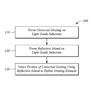
method of fabricating a diffractive backlight is provided. Figure 3
illustrates flow chart
of a method 100 of fabricating a diffractive backlight in an example,
according to an
embodiment consistent with the principles described herein. As illustrated,
the method
100 of fabricating a diffractive backlight comprises forming 110 a universal
grating on a
light guide substrate. In some embodiments, forming 110 a universal grating
may
provide the universal grating on or adjacent to a surface of the light guide
substrate. In
Date Recue/Date Received 2021-10-08
CA 03136670 2021-10-08
-13-
other embodiments, the universal grating may be provided on surface of a layer
of optical
material that is, in turn, on a surface of the light guide substrate.
[0044] According to various embodiments, forming 110 a universal grating
may
employ any of a variety of different patterning methods including, but not
limited to,
photolithography, focused ion beam lithography, and electron beam lithography,
and
nanoimprint lithography (NIL). In particular, in some embodiments, forming 110
a
universal grating on the light guide substrate may comprise nanoimprinting the
universal
grating nanoimprinting the universal grating in a nanoimprint receiving layer
of the light
guide substrate using a nanoimprint mold. In some embodiments, the nanoimprint
receiving layer may comprise a material of the light guide substrate, e.g., a
surface of the
light guide substrate itself. In other embodiments, the nanoimprint receiving
layer may
comprise a layer or material deposited or provided on the surface of the light
guide
substrate. For example, the layer may be a layer of optical material that is
formable
according to nanoimprint lithography having an index of refraction that is
matched to an
index of refraction of the light guide substrate, e.g., a layer of poly(methyl
methacrylate)
(PMMA) on a surface of a glass or PMMA light guide substrate.
[0045] The method 100 of fabricating a diffractive backlight illustrated
in Figure
3 further comprises forming 120 a reflective island on the light guide
substrate.
According to some embodiments, forming 120 the reflective island comprises
patterning
a layer of reflective material to define the reflective island. The layer of
reflective
material may comprise one or more of a metal, a metal polymer (e.g., polymer
aluminum), and a high-index dielectric, according to various embodiments. For
example,
the layer of reflective material may be deposited by or using one or more of
evaporative
deposition, sputter deposition, or an equivalent. Then the reflective material
layer may be
patterned using photolithography or imprint lithography, for example. In
another
example, the reflective island may be formed 120 comprising ink stamping,
screen
printing, or a similar printing process. In yet another example, forming 120
the reflective
island may employ preform deposition in which a reflective island preform is
employed.
[0046] In some embodiments, the universal grating is located on a
surface of the
light guide substrate and the reflective island is formed 120 over the
universal grating. As
such, forming 110 the universal grating is performed before forming 120 the
reflective
Date Recue/Date Received 2021-10-08
CA 03136670 2021-10-08
-14-
island. In particular, in some embodiments, forming 120 the reflective island
comprises
depositing the layer of reflective material over the universal grating, and
then etching the
reflective material layer using a patterned photoresist to remove a portion of
the reflective
material layer and define the reflective island.
[0047] In other embodiments, forming 120 the reflective island is
performed
before forming 110 the universal grating. For example, the reflective island
may be
formed 120 on a surface of the light guide substrate and then the universal
grating may be
formed 110 in a receiving layer that is applied over the reflective island. As
a result, the
reflective island may be located on a surface of the light guide substrate and
the universal
grating is then formed 110 over the reflective island.
[0048] As illustrated in Figure 3, the method 100 of fabricating a
diffractive
backlight further comprises selecting 130 a portion of the universal grating
using the
reflective island to define a grating element. The grating element that is
defined by
selecting 130 represents a diffraction grating that comprises a relatively
small portion of
the original universal grating. Further, the defined grating element has a
size and a
location on the light guide substrate that is determined by the reflective
island. For
example, the grating element may be substantially similar in size and also may
be
substantially collocated or aligned with the reflective island as a result of
selecting 130
the universal grating portion. According to various embodiments, a reflective
diffraction
grating element of the diffractive backlight comprises a combination of the
grating
element and the reflective island.
[0049] In some embodiments, selecting 130 a portion of the universal
grating
using the reflective island to define a grating element comprises removing an
exposed
portion of the universal grating that is not covered by the reflective island
by etching the
exposed portion. In particular, selecting 130 may employ the reflective island
as a
photomask to photolithographically define the grating element.
[0050] For example, selecting 130 a portion of the universal grating may
comprise
applying a photoresist to cover the universal grating. The photoresist is then
exposed
using a collimated light source to illuminate the photoresist from a side of
the light guide
substrate that is opposite to a side on which the reflective island is
located. According to
various embodiments, the photoresist may be a positive photoresist and the
reflective
Date Recue/Date Received 2021-10-08
CA 03136670 2021-10-08
-15-
island serves as a photomask to define a portion of the photoresist that
remains after the
photoresist is developed. Selecting 130 the portion of the universal grating
to define the
grating element then further comprises removing an exposed portion of the
universal
grating not covered by the photoresist that remains. For example, removing the
exposed
portion of the universal grating may comprise etching the exposed portion to
remove
material of the universal grating not covered by the photoresist.
[0051] In other embodiments, selecting 130 may employ etching or a
similar
process to remove a portion or portions of the universal grating to define the
grating
element, the reflective island being employed as an etch mask. In yet other
embodiments,
selecting 130 the portion of the universal grating using the reflective island
to define a
grating element comprises covering the universal grating and reflective island
with a layer
of optical material, the optical material layer being index-matched to the
universal
grating.
[0052] In some embodiments (not illustrated in Figure 3), the method 100
of
fabricating a diffractive backlight further comprises applying a negative
photoresist to
cover reflective island and the grating element. Following application, the
negative
photoresist may be exposed using a collimated light source to illuminate the
negative
photoresist and define an opening in the photoresist above the grating
element. Then, a
reflective material may be deposited on the grating element through the
opening in the
photoresist. As a result, the reflective material may exclusively cover the
grating
element.
[0053] In some embodiments, a layer of optical material may be deposited
on the
light guide substrate such that the optical material layer embeds the grating
element, the
reflective island, and the reflective material covering the grating element.
The exposed
portion of the universal grating that is removed is the exposed portion that
is covered by
the optical material layer.
[0054] Figure 4 illustrates flow chart of a method 200 of fabricating a
diffractive
backlight in another example, according to an embodiment consistent with the
principles
described herein. As illustrated in Figure 4, the method 200 of fabricating a
diffractive
backlight comprises forming 210 a reflective island on a surface of a light
guide. In
various embodiments, the reflective island may comprise, but is not limited
to, one or
Date Recue/Date Received 2021-10-08
CA 03136670 2021-10-08
-16-
more of a metal, a metal polymer, and a high-index dielectric. In some
embodiments,
forming 210 a reflective island may be substantially similar to forming 120 a
reflective
island described above with respect to the method 100 of fabricating a
diffractive
backlight. For example, the reflective island may be formed 210 using
photolithographic
patterning of a deposited layer of reflective material. Further, the light
guide may be
substantially similar to the light guide substrate of the above-described
method 100 of
fabricating a diffractive backlight, in some embodiments.
[0055] As illustrated in Figure 4, the method 200 of fabricating a
diffractive
backlight further comprises depositing 220 a layer of optical material on the
light guide to
cover the reflective island. In various embodiments, the optical material is
index-matched
to a material of the light guide. For example, the light guide may comprise
glass or
poly(methyl methacrylate) (PMMA) and the optical material may comprise PMMA,
both
having a refractive index of about 1.5.
[0056] The method 200 of fabricating a diffractive backlight illustrated
in Figure
4 further comprises forming 230 a universal grating on the optical material
layer. In some
embodiments, forming 230 a universal grating may be substantially similar to
forming
110 a universal grating, as described above with respect to the method 100 of
fabricating
a diffractive backlight. For example, forming 230 a universal grating may use
nanoimprint lithography, in some embodiments.
[0057] According to various embodiments, the method 200 of fabricating a
diffractive backlight further comprises selecting 240 a portion of the
universal grating
using the reflective island to define a grating element. In various
embodiments, a
reflective diffraction grating element of the diffractive backlight comprises
a combination
of the grating element and the reflective island. In some embodiments,
selecting 240 a
portion of the universal grating may be substantially similar to selecting 130
a portion of
the universal grating of the above-described method 100 of fabricating a
diffractive
backlight. For example, selecting 240 may comprise applying a photoresist to
cover the
universal grating and the exposing the photoresist using a collimated light
source to
illuminate the photoresist from a side of the light guide that is opposite to
a side on which
the reflective island is located, where the reflective island serves as a
photomask.
Further, selecting 240 a portion of the universal grating to define the
grating element may
Date Recue/Date Received 2021-10-08
CA 03136670 2021-10-08
-17-
comprise one of etching an exposed portion of the universal grating not
covered by the
photoresist that remains or covering the exposed portion of the universal
grating with a
layer of the optical material, for example.
[0058] Figure 5 illustrates flow chart of a method 300 of fabricating a
diffractive
backlight in another example, according to an embodiment consistent with the
principles
described herein. As illustrated in Figure 5, the method 300 of fabricating a
diffractive
backlight comprises forming 310 a universal grating on a surface of a light
guide by
nanoimprinting the universal grating using a nanoimprint mold. In some
embodiments,
forming 310 a universal grating may be substantially similar to forming 110 a
universal
grating of the method 100 of fabricating a diffractive backlight, as described
above.
[0059] The method 300 of fabricating a diffractive backlight illustrated
in Figure
further comprises forming 320 a reflective island over the universal grating
and
selecting 330 a portion of the universal grating using the reflective island
to define a
grating element. As described above, a reflective diffraction grating element
of the
diffractive backlight may comprise a combination of the grating element and
the
reflective island. In some embodiments, one or both of forming 320 a
reflective island
and selecting 330 a portion of the universal grating may be substantially
similar to the
above-described forming 120 a reflective island and forming 110 a universal
grating,
respectively. For example, forming 320 the reflective island over the
universal grating
may comprise patterning a layer of reflective material to define the
reflective island, the
layer of reflective material comprising one or more of a metal, a metal
polymer, and a
high-index dielectric.
[0060] In some embodiments, selecting 330 the portion of the universal
grating
using the reflective island to define a grating element comprises removing an
exposed
portion of the universal grating that is not covered by the reflective island
by etching the
exposed portion. In other embodiments, selecting 330 the portion of the
universal grating
comprises covering the universal grating and reflective island with a layer of
optical
material, the optical material layer being index-matched to the universal
grating.
[0061] In some embodiments, the universal grating may comprise openings
in the
universal grating. The openings may be provided by photolithographic
processing (e.g.,
etching of the universal grating), for example. In these embodiments, the
method 300
Date Recue/Date Received 2021-10-08
CA 03136670 2021-10-08
-18-
may further comprise depositing a layer of reflective material in the openings
to provide
reflective islands that are not reflective diffraction grating elements.
EXAMPLES
[0062] Several examples of diffractive backlight fabrication according
to one or
more of above-described methods 100, 200, 300 are presented below. The
examples
illustrate results of employing the aforementioned methods, by way of example
and not
limitation.
[0063] Figures 6A-6G illustrate cross sectional views of fabricating a
diffractive
backlight 400 in an example, according to an embodiment of the principles
described
herein. In particular, Figures 6A-6C illustrate the diffractive backlight 400
comprising a
light guide substrate 410. In some embodiments, the light guide substrate 410
may
substantially similar to either the light guide substrate or the light guide
described above
with respect to the method 100, 200, 300 of fabricating a diffractive
backlight. In
particular, a light guide of the diffractive backlight 400 may comprise the
light guide
substrate 410, according to various embodiments.
[0064] As illustrated in Figure 6A, a universal grating 420 is provided
on a
surface of the light guide substrate 410. The universal grating 420 generally
extends
across an entire surface or substantially an entire surface of the light guide
substrate 410.
In some embodiments, the universal grating 420 may be substantially similar to
the
universal grating provided by forming 110 a universal grating that is
described above
with respect to the method 100, 300 of fabricating a diffractive backlight.
For example,
the universal grating 420 may be provided on the light guide substrate 410
using
nanoimprint lithography.
[0065] Figure 6B illustrates a reflective island 430 formed over and
covering a
portion 422 of the universal grating 420. Further, as illustrated in Figure
6B, another
portion 424 of the universal grating 420 is exposed and not covered by the
universal
grating 420. According to some embodiments, the reflective island 430 may be
substantially similar to the reflective island described above as being
provided by forming
120, 320 a reflective island of the above-described method 100, 300 of
fabricating a
diffractive backlight.
Date Recue/Date Received 2021-10-08
CA 03136670 2021-10-08
-19-
[0066] In various embodiments, the exposed portion 424 may be removed to
define a grating element 426 of the diffractive backlight 400. In particular,
in some
embodiments, the exposed portion 424 may be removed by covering the universal
grating
420 and the reflective island 430 with a layer of optical material 440 that
index-matched
to a material of the universal grating 420, as illustrated in Figure 6C. As
described above,
the optical material 440 has a refractive index that is substantially similar
to a refractive
index of the universal grating 420 such that covering the universal grating
420 effectively
eliminates any diffractive features thereof in the exposed portion 424. In
other
embodiments, as illustrated in Figure 6D, the exposed portion 424 of the
universal grating
420 may be removed by etching the exposed portion 424 using the reflective
island 430
as an etch mask.
[0067] Removal of the exposed portion 424 selects the portion 422 of the
universal grating as the grating element 426. According to some embodiments,
the
removal of the exposed portion 424 may represent selecting 130, 330 a portion
of the
universal grating 420 using the reflective island 430 to define the grating
element, as
described with respect to the method 100, 300 of fabricating a diffractive
backlight. For
example, in Figure 6C the reflective island 430 effectively protects the
covered portion
422 to select and define the grating element 426 when the optical material
layer is
applied, while in Figure 6D the reflective island 430 selects and defines the
grating
element 426 by acting as an etch resist preventing the covered portion 422
from being
etched away.
[0068] Once defined, the grating element 426 in conjunction with the
reflective
island 430 may represent a reflective diffraction grating element 402 of the
diffractive
backlight 400. In some embodiments (e.g., Figure 6C), the reflective
diffraction grating
element 402 is embedded in a light guide that comprises the light guide
substrate 410 and
the layer of optical material 440. In other embodiments (e.g., Figure 6D), the
reflective
diffraction grating element 402 may be on or at a surface of the light guide
substrate 410
that serves as the light guide of the diffractive backlight 400.
[0069] In some embodiments, the universal grating 420 may comprise
openings in
the universal grating 420. In addition, a layer of reflective material may be
deposited in
the openings to provide reflective islands that are not part of or included in
a reflective
Date Recue/Date Received 2021-10-08
CA 03136670 2021-10-08
-20-
diffraction grating element, in some embodiments. Figure 6E illustrates a top
view and
Figure 6F illustrates a side view of the diffractive backlight 400 depicting a
plurality of
openings 428 in the universal grating 420. Also illustrated are reflective
islands 432
located within each opening 428 of the opening plurality, by way of example
and not
limitation. As illustrated in Figure 6F, the reflective islands 432 within the
openings 428
do not cover any of the universal grating 420 and therefore are not part of a
reflective
diffraction grating element. On the other hand, following selection and
definition of the
grating element 426, the reflective island 430 and the grating element 426
(including a
covered portion of the universal grating) are part of a reflective diffraction
grating
element 402, as illustrated in Figure 6G.
[0070] Figures 7A-7F illustrate cross sectional views of fabricating a
diffractive
backlight 400 in another example, according to an embodiment of the principles
described herein. As in Figures 6A-6F, the diffractive backlight 400
illustrated in Figures
7A-7F comprise the light guide substrate 410. Further, Figure 7A illustrates
the reflective
island 430 formed on a surface of the light guide substrate 410. The
reflective island 430
and forming same may be substantially similar to the reflective island
provided by
forming 120, 210 a reflective island on a light guide substrate or light guide
of the above-
described method 100, 200 of fabricating a diffractive backlight, according to
some
embodiments.
[0071] Figure 7B illustrates the light guide substrate 410 and
reflective island 430
of the diffractive backlight 400 covered by a layer of optical material 440
that has been
deposited on the light guide substrate 410 and over the reflective island 430.
As
illustrated, the optical material 440 may be index-matched to the light guide
substrate
410, i.e., the optical material 440 may have a refractive index that is
substantially similar
to a refractive index of the light guide substrate 410. In some embodiments,
the layer of
optical material 440 may be deposited on the light guide substrate 410
according to
depositing 220 a layer material of the above-described method 200 of
fabricating a
diffractive backlight.
[0072] Figure 7C illustrates a universal grating 420 provided or formed
in a
receiving layer of the optical material 440. In some embodiments, a surface of
the layer
of optical material 440 may serve as the receiving layer. In other embodiments
(not
Date Recue/Date Received 2021-10-08
CA 03136670 2021-10-08
-21-
illustrated), another layer of material may be provided on or applied to the
optical
material surface to serve as the receiving layer. The universal grating 420
may be provide
or formed according to forming 110, 230, 310 a universal grating of method
100, 200,
300 of fabricating a diffractive backlight, as described above.
[0073] Figure 7D illustrates a positive photoresist 450 applied over the
universal
grating 420. Also illustrated are arrows representing exposure of the positive
photoresist
450 using a collimated light source to illuminate the positive photoresist 450
from a side
of the light guide substrate 410 that is opposite to a side on which the
reflective island
430 is located. As illustrated, the reflective island 430 serves as a
photomask to define a
portion 452 of the positive photoresist 450 that remains after the positive
photoresist 450
is developed. Another portion 454 of the photoresist is removed by developing
the
positive photoresist 450. In particular, as illustrated in Figure 7D, the
reflective island
430 blocks some light (arrows) from the collimated light source, preventing
the blocked
light from reaching and illuminating (i.e., exposing) the portion 452 of the
positive
photoresist 450 that is immediately above the reflective island 430, as
illustrated. The
other portion 454 of the positive photoresist 450 is exposed to the light from
the light
source, as illustrated, allowing the other portion 454 to be removed during
when the
positive photo resist is developed.
[0074] Figure 7E illustrates the portion 452 of the positive photoresist
450 that
remains after the positive photoresist 450 is developed. The remaining portion
452
covers and protects a portion 422 of the universal grating 420, while other
portions 424 of
the universal grating 420 are not protected and therefore are exposed portions
424.
According to various embodiments, the portion 422 of the universal grating 420
may be
selected, or more particularly further selected, to define the grating element
426 by
removing the exposed portions 424 of the universal grating 420 not covered by
the
remaining portion 452 of the positive photoresist 450. For example, the
exposed portion
424 of the universal grating 420 may be removed by etching.
[0075] Figure 7F illustrates the diffractive backlight 400 following
removal of the
remaining portion of positive photoresist. As illustrated in Figure 7F, the
reflective
diffraction grating element 402 comprises the reflective island 430 below and
aligned
with the grating element 426.
Date Recue/Date Received 2021-10-08
CA 03136670 2021-10-08
-22-
[0076] Figures 8A-8G illustrate cross sectional views of fabricating a
diffractive
backlight 400 in yet another example, according to an embodiment of the
principles
described herein. As in Figures 6A-6F and 7A-7F, the diffractive backlight 400
illustrated in Figures 8A-8G comprise the light guide substrate 410. Further,
Figure 8A
illustrates the reflective island 430 formed on a surface of the light guide
substrate 410.
The reflective island 430 may be provided as described above. For example, the
reflective island 430 may be formed using photolithographic patterning of a
reflective
material layer applied to the light guide substrate surface.
[0077] Figure 8B illustrates the universal grating 420 provided over the
reflective
island 430 on the surface of the light guide substrate 410. As described
above, the
universal grating 420 may be provided on the light guide substrate 410 surface
using
nanoimprint lithography. For example, a receiving layer comprising an optical
material
layer (e.g., a layer of the index-matched optical material 440) may be
deposited on the
light guide substrate 410 surface and over the reflective island. Then a
nanoimprint mold
may be used to nanoimprint the universal grating 420, for example.
[0078] As illustrated in Figure 8C, a positive photoresist 450 may be
applied over
the universal grating 420 and the reflective island 430 may be used as a
photomask to
define a portion 452 of the positive photoresist 450 that remains after the
positive
photoresist is developed. For example, Figure 8C illustrates arrows
representing
exposure of the positive photoresist 450 using a collimated light source to
illuminate the
positive photoresist 450 from a side of the light guide substrate 410 that is
opposite to a
side on which the reflective island 430 is located, e.g., as described above
with respect to
Figure 7D. Also, as described previously, another portion 454 of the
photoresist is
removed by developing the positive photoresist 450 to leave the remaining
portion 452.
Further, as described above, the remaining portion 452 selects the portion 422
of the
universal grating 420 to define the grating element 426.
[0079] Figure 8D illustrates the grating element 426 after removal of
the exposed
portion of the universal grating 420 that is not covered by the remaining
portion 452 of
the positive photoresist 450 following photoresist development. Etching may be
used to
remove the exposed portion to provide the grating element 426 on the
reflective island
430, as illustrated.
Date Recue/Date Received 2021-10-08
CA 03136670 2021-10-08
-23-
[0080] According to some embodiments, the grating element 426 may be
coated
with a layer of reflective material. The reflective material layer may be
relatively thin
such that coating of the grating element 426 preserves a diffraction grating
of the grating
element 426 in the reflective material layer, according to various
embodiments.
[0081] Figure 8E illustrates using a negative photoresist 460 that is
exposed using
the collimated light as described above followed by deposition of the
reflective material
470 to provide a reflective material layer coating on the grating element 426.
In
particular, developing the negative photoresist 460 after using the reflective
island 430 as
a photomask exposes the grating element 426. The reflective material 470 may
then be
deposited using sputtering, evaporative deposition, or a similar method to
coat both the
exposed portion 462 of the negative photoresist 460 and the exposed grating
element 426.
[0082] As illustrated in Figure 8F, removal of the exposed portion 462
of the
negative photoresist 460 and concomitant lift-off of reflective material 470
that is not
covering the grating element 426, leaves behind the reflective island 430 and
the grating
element 426 with a coating of the reflective material 470. A thickness of the
negative
photoresist 460 may be chosen to support lift-off of the reflective material
470 on the
exposed portion 462 of the negative photoresist 460, according to various
embodiments.
[0083] Figure 8G illustrates the diffractive backlight 400 after
deposition of an
index-matched optical material 440 to cover the reflective island 430 and
reflective
material-coated grating element 426, according to some embodiments. As
illustrated, a
light guide of the diffractive backlight 400 comprise a combination of the
index-matched
optical material 440 and light guide substrate 410. Further, a reflective
diffraction grating
element 402 of the diffractive backlight 400 comprises the reflective island
430 and the
aligned grating element 426 with the coating of the reflective material 470.
[0084] Figures 9A-9E illustrate cross sectional views of fabricating a
diffractive
backlight 400 in yet another example, according to an embodiment of the
principles
described herein. Figure 9A illustrates the light guide substrate 410 and
reflective island
430 of the diffractive backlight 400 covered by a universal grating 420, e.g.,
as described
with respect to Figures 8A-8B above. The universal grating 420 may be provide
or
formed according to forming 110, 230, 310 a universal grating of method 100,
200, 300
of fabricating a diffractive backlight, as described above. In particular,
nanoimprint
Date Recue/Date Received 2021-10-08
CA 03136670 2021-10-08
-24-
lithography using a nanoimprint mold may be used to form the universal grating
420, for
example.
[0085] Figure 9B illustrates a negative photoresist 460 that has been
applied over
the universal grating 420. Also illustrated are arrows representing exposure
of the
negative photoresist 460 using a collimated light source to illuminate the
negative
photoresist 460 from a side of the light guide substrate 410 that is opposite
to a side on
which the reflective island 430 is located. As illustrated, the reflective
island 430 serves
as a photomask to define the exposed portion 462 that remains after the
negative
photoresist 460 is developed. Another portion 464 of the negative photoresist
460 is
removed by developing the negative photoresist 460 to expose a portion 422 of
the
universal grating 420 that is aligned with the reflective island 430. As a
result, the
reflective island 430 is used to select the portion 422 and define the grating
element 426.
[0086] Figure 9C illustrates a layer of reflective material 470
deposited on the
negative photoresist 460 and exposed portion 422 of the universal grating 420.
As above,
the reflective material 470 may be thin enough to preserve a diffraction
grating of the
universal grating in the deposited reflective material layer.
[0087] Figure 9D illustrates a portion 472 of the reflective material
layer that
remains on the universal grating 420 following removal of the exposed portion
462 of the
negative photoresist 460 and concomitant lift-off of the reflective material
470. As
illustrated, the remaining portion 472 of the reflective material layer is
aligned with the
reflective island and effectively defines the grating element 426. That is,
exposure of the
negative photoresist 460 using the reflective island 430 as a photomask,
followed by
deposition and lift-off of the reflective material layer selects the portion
422 of the
universal grating 420 and defines the grating element 426.
[0088] Figure 9E illustrates the diffractive backlight 400 after
deposition of an
index-matched optical material 440 to cover the reflective island 430 and
reflective
material-coated grating element 426. As illustrated, a light guide of the
diffractive
backlight 400 comprise a combination of the index-matched optical material 440
and light
guide substrate 410. Further, a reflective diffraction grating element 402 of
the
diffractive backlight 400 comprises the reflective island 430 and the aligned
grating
element 426 with the coating of the reflective material 470.
Date Recue/Date Received 2021-10-08
CA 03136670 2021-10-08
-25-
[0089] Thus, there have been described examples and embodiments of
several
methods of fabricating a diffractive backlight that employ a reflective island
to select a
portion of a universal grating as or to define a grating element, wherein the
reflective
island and the grating element comprise a reflective diffraction grating
element of the
diffractive backlight. It should be understood that the above-described
examples are
merely illustrative of some of the many specific examples that represent the
principles
described herein. Clearly, those skilled in the art can readily devise
numerous other
arrangements without departing from the scope as defined by the following
claims.
Date Recue/Date Received 2021-10-08