Note: Descriptions are shown in the official language in which they were submitted.
CA 03138101 2021-10-26
WO 2020/231405
PCT/US2019/032114
Subcutaneous Analyte Sensor Applicator and Continuous
Monitoring System
BACKGROUND OF THE INVENTION
[0001] 1. Field of the Invention
[0002] The present invention relates generally to continuous analyte
monitoring. More particularly, the present invention relates to an analyte
monitoring system having a subcutaneous insertable analyte sensor, an inserter
assembly and reader.
[0003] 2. Description of the Prior Art
[0004] Continuous analyte monitoring devices have been developed for
implanting into a patient's skin. Continuous monitoring systems typically use
a
tiny implantable sensor that is inserted under the skin, or into the
subcutaneous
fat layer to check analyte levels in the tissue fluid. A transmitter sends
information about the analyte levels by way of, for example, a wire to a
monitor or
wirelessly by radio waves from the sensor to a wireless monitor. These devices
are typically implanted for three to seven days of use to monitor in real-time
a
patient's glucose level.
[0005] One such device is disclosed in PCT International Application
Publication No. WO 2018/118061 to Thomas H. Peterson et al. A continuous
glucose monitoring system and method is disclosed and has an inserter assembly
for inserting a sensor through the skin and into subcutaneous tissue where an
inserter housing with the sensor remains on the skin after insertion, a sensor
housing cover attachable to the sensor housing after insertion where the
sensor
housing cover has an electronic module and a battery, and an electronic device
equipped with wireless communication for communicating with the electronic
module of the sensor housing cover assembly, the electronic device configured
for receiving input signals from the sensor, converting the input signals to
analyte
date, displaying the analyte data on a user interface of the electronic
device,
storing the data for recall, and creating and/or sending reports of the data.
1
CA 03138101 2021-10-26
WO 2020/231405
PCT/US2019/032114
[0006] U.S. Patent Application Publication No. 2018/0235520 to Vivek Rao et
al. Systems, devices and methods are provided for inserting at least a portion
of
an in vivo analyte sensor, such as a dermal sensor, for sensing an analyte
level in
a bodily fluid of a subject. An applicator is positioned against a skin
surface and a
force is applied to the applicator causing at least a portion of a sharp and
an in
vivo analyte sensor to be positioned in the body of the subject. In
particular,
disclosed herein are embodiments of applicators designed to prevent premature
sharp withdrawal and/or reduce the likelihood of improper sensor insertion.
Also
disclosed are embodiments of applicators including sharp modules having an
angled sharp which can be configured to create an insertion path for a sensor.
[0007] U.S. Patent Application Publication No. 2016/0058344 to Vivek Rao et
al. Systems, devices, and methods are provided for the assembly and
subsequent delivery of an in vivo analyte sensor. An applicator with sensor
electronics is inserted into a tray containing an assembly that includes a
sharp
and an analyte sensor. The insertion causes the assembly to couple with the
sensor electronics and form a deliverable sensor control device retained
within
the applicator, which can then be placed in position on a body of a user to
monitor
that user's analyte levels.
[0008] U.S. Patent Application Publication No. 2016/0058344 to Thomas H.
Peterson et al. The device is an apparatus for the subcutaneous implantation
of
in-vivo sensors. The device is an inserter assembly for continuous glucose
monitoring with medication delivery capability where the assembly has a
deployment button containing a needle deployment mechanism having a sharp
held in a pre-release position, a housing body in which the deployment button
is
movably received within a top end of the housing body where the housing body
has a sensor deployment assembly containing a lumen and a sensor disposed
within the lumen and extending out of the lumen to a circuit board that is
part of
the sensor deployment assembly. The sensor deployment assembly matingly
connects to the sharp where the sharp extends beyond the sensor deployment
assembly and contains the sensor not fixedly attached to the sharp, and a
sensor
housing releasably received within a lower end of the housing body. The sharp
extends into a sensor deployment assembly recess within the sensor housing and
directly above a sensor opening in a bottom of the sensor housing.
2
CA 03138101 2021-10-26
WO 2020/231405
PCT/US2019/032114
[0009] U.S. Patent No. 10,213,139 to Vivek Rao et al. discloses systems,
devices, and methods for the assembly and subsequent delivery of an in vivo
analyte sensor. An applicator with sensor electronics is inserted into a tray
containing an assembly that includes a sharp and an analyte sensor. The
insertion causes the assembly to couple with the sensor electronics and form a
deliverable sensor control device retained within the applicator, which can
then be
placed in position on a body of a user to monitor that user's analyte levels.
[0010] U.S. Patent No. 10,010,280 to Manuel L. Donnay et al. discloses an
apparatus for insertion of a medical device in the skin of a subject is
provided, as
well as methods of inserting medical devices. Embodiments include removing a
substantially cylindrical cap from an inserter to expose a substantially
cylindrical
sleeve, removing a cover from a substantially cylindrical container holding
sensor
components, and fitting the sensor components into the inserter.
[0011] U.S. Patent No. 9,788,771 to Gary A. Stafford discloses an automatic
sensor inserter for placing a transcutaneous sensor into the skin of a living
body.
According to aspects of the invention, characteristics of the insertion such
as
sensor insertion speed may be varied by a user. In some embodiments, insertion
speed may be varied by changing an amount of drive spring compression. The
amount of spring compression may be selected from a continuous range of
settings and/or it may be selected from a finite number of discrete settings.
Methods associated with the use of the automatic inserter are also covered.
[0012] U.S. Patent No. 9,750,444 to Gary A. Stafford discloses systems and
methods for providing a compressible interconnect for allowing electrical
communication between an electronics unit and an analyte sensor in an on-body
analyte monitoring device. In other embodiments, systems and methods are
provided for reducing the Z-height of an on-body analyte monitoring device by
utilizing novel interconnects.
[0013] U.S. Patent No. 9,402,570 to Louis Pace et al. discloses devices
associated with on-body analyte sensor units are disclosed. These devices
include any of packaging and/or loading systems, applicators and elements of
the
on-body sensor units themselves. Also, various approaches to connecting
electrochemical analyte sensors to and/or within associated on-body analyte
sensor units are disclosed. The connector approaches variously involve the use
3
CA 03138101 2021-10-26
WO 2020/231405
PCT/US2019/032114
of unique sensor and ancillary element arrangements to facilitate assembly of
separate electronics assemblies and sensor elements that are kept apart until
the
end user brings them together.
[0014] U.S. Patent No. 5,299,571 to John Mastrototaro discloses a device
for
implantation of in-vivo sensors. The apparatus includes a housing, a dual-
lumen
tube extending therefrom, and an in-vivo sensor received within one of the
lumens of the tube. A needle is received within the other lumen of the tube,
and
is used to insert the tube through the skin. After implantation, the needle is
removed, and the flexible tube and sensor remain beneath the skin.
[0015] U.S. Patent Application Publication 2010/0022863 (2010, Mogensen et
al.) discloses an inserter for a transcutaneous sensor. The inserter includes
a
needle unit and a sensor housing. The needle unit includes a needle hub and a
carrier body. The sensor housing and the needle hub are releasably connected
and when they are connected, the insertion needle is placed along the sensor
(e.g. surrounding the sensor wholly or partly). The carrier body guides the
movement relative to the housing between a retracted and an advanced position.
When released, the needle unit and the sensor housing are forced by a spring
unit to an advanced position where the needle and sensor are placed
subcutaneously. Upwardly-bent parts on the leg of the housing set the
insertion
angle of about 30 into the skin of the patient.
[0016] U.S. Patent Application Publication 2012/0226122 (2012, Meuniot et
al.) discloses an inserter device for an analyte sensor. The device includes a
housing that is positioned above the subcutaneous fat layer, a blade shuttle,
and
a sensor shuttle. A spring is compressed between the blade shuttle and the
sensor shuttle. The blade shuttle and sensor shuttle move towards the
subcutaneous fat layer. When a spring force is released by the spring, the
blade
shuttle moves towards and pierces into the subcutaneous fat layer creating a
pathway into the subcutaneous fat layer. The analyte sensor is implanted by
the
sensor shuttle by following the blade shuttle into the pathway created by the
blade
shuttle. The blade shuttle is then retracted from the subcutaneous fat layer,
leaving the analyte sensor in the fat layer.
[0017] U.S. Patent Application Publication 2013/0256289 (2013, Hardvary et
al.) discloses a diagnostic device. The diagnostic device has partially
retractable
4
CA 03138101 2021-10-26
WO 2020/231405
PCT/US2019/032114
hollow guide needles for the intradermal placement of diagnostic elements
fixedly
connected to measuring means within this device. This obviates the need to
remove the guide needle and to connect the diagnostic elements to the
measuring means after placement into the skin.
SUMMARY OF THE INVENTION
[0018] In the present disclosure, the term "substantially simultaneously"
means
that the individual actions that occur within a subcutaneous sensor insertion
applicator of the present invention when the insertion applicator is activated
by a
user/patient to insert a sensor subcutaneously in the skin of a patient (i.e.
to
assemble the sensor module as a single unit, to insert the sensor
subcutaneously, to retract the needle assembly, to turn on the power switch to
the
electro-sensor assembly, to release the sensor module from the applicator
module, and to release the applicator module from the surface of the skin)
cannot
be perceived by a human during the sensor insertion process.
[0019] It is an object of the present invention to provide an all-
inclusive, single
use, continuous analyte monitoring system.
[0020] The present invention achieves these and other objectives by
providing
continuous analyte monitoring system and method that includes an applicator
module for inserting a sensor through the skin and into subcutaneous tissue
where a sensor module remains on the skin after insertion and an electronic
display device such as, for example, a smart phone and the like that is
equipped
with wireless communication for communicating with the sensor module, the
electronic display device configured for receiving input signals from the
sensor,
converting the input signals to analyte data, displaying the analyte data on a
user
interface of the electronic device, storing the data for recall, and creating
and/or
sending reports of the data. Various sensors, needles and electronic display
devices are disclosed in PCT Patent Application Publication No. WO
2018/118061 to Thomas H. Peterson et al., which publication is herein
incorporated by reference in its entirety.
[0021] In one embodiment, there is disclosed an all-inclusive, single-use,
subcutaneous analyte sensor applicator and monitoring system. The system
includes an inserter module and a sensor module. The inserter module includes
CA 03138101 2021-10-26
WO 2020/231405
PCT/US2019/032114
an applicator housing, a deployment button where the applicator housing is
partially received within a button chamber, and a pre-loaded insertion
assembly
completely disposed and secured within the button chamber and partially
disposed within the applicator housing chamber when the deployment button is
in
an initial, loaded position. The pre-loaded insertion assembly includes an
assembly housing, a biasing element disposed within an assembly housing
chamber, and a needle assembly disposed within the assembly housing chamber
where the biasing element is in a compressed state between the needle assembly
and an assembly housing bottom. The sensor module includes a sensor lower
housing releasably connected to the applicator housing, a sensor upper housing
removably retained against the insertion assembly housing and spaced from the
sensor lower housing, and an electro-sensor assembly disposed within the
sensor
upper housing where (a) the electro-sensor assembly has an electronic circuit
with a power switch and a sensor electrically coupled to the electronic
circuit and
(b) where the sensor is temporarily disposed within a needle of the needle
assembly when the applicator system is in the initial pre-loaded position.
[0022] In another aspect of the invention, the applicator housing has an
applicator elongated body defining the applicator housing chamber, a proximal
internal body flange portion and an applicator housing retaining arm adjacent
a
proximal applicator housing end.
[0023] In another embodiment, the deployment button has a button elongated
body defining the button chamber, a closed button distal end and a button
retaining arm extends within the button chamber from the closed button distal
end
toward an open button proximal end a predefined distance.
[0024] In one embodiment, the assembly housing has an assembly housing
body having an assembly circumferential wall defining the assembly housing
chamber, a closed housing proximal end, a recessed housing bottom at the
closed housing proximal end, an open housing distal end, an assembly housing
retaining arm formed in the assembly circumferential wall and extending toward
the closed housing proximal end, a plurality of housing retaining fingers
formed in
the assembly circumferential wall and extending toward and beyond the closed
housing proximal end and having an inward-facing housing finger hook surface,
an assembly housing locking slot that interacts with the button retaining arm
to
6
CA 03138101 2021-10-26
WO 2020/231405
PCT/US2019/032114
secure the pre-loaded insertion assembly within the button chamber, and a
needle assembly locking slot that interacts with the needle body retaining
arm.
[0025] In one embodiment, the biasing element is positioned on one end
against a recessed housing bottom of the assembly housing.
[0026] In one embodiment, the needle assembly has a needle body with a
needle body circumferential wall, a closed needle body distal end forming a
needle body top, an open needle body proximal end where the needle body
retaining arm is formed in the needle body circumferential wall to thereby
position
an outward-facing needle retaining arm hook surface adjacent to the closed
needle body distal end, and a needle receiving portion formed in the needle
body
top where a needle is secured adjacent a needle distal end and extends
parallel
to the needle body circumferential wall a predefined distance beyond the open
needle body proximal end and where the biasing element is positioned against
the closed needle body distal end through the open needle body proximal end.
The outward-facing needle is offset from a central axis of the insertion
applicator.
[0027] In one embodiment, the sensor lower housing has a plurality of lower
housing locking elements extending upward a predefined distance from a lower
housing bottom into the applicator housing chamber.
[0028] In one embodiment, the sensor lower housing has a lower housing
locking recess in a lower housing wall where the applicator housing retaining
arm
engages the lower housing locking recess when the deployment button is in the
initial pre-loaded position.
[0029] In one embodiment, the sensor upper housing has an upper housing
circumferential wall extending from the upper housing top forming a housing
top
flange portion in a perimeter of the upper housing top. The upper housing
circumferential wall has a plurality of upper housing locking recesses adapted
for
mating connection to a plurality of locking elements of the sensor lower
housing.
[0030] In one embodiment, the electro-sensor assembly includes a power
source coupled between the electronic circuit and the power switch.
[0031] In another embodiment of the inserter assembly, the bottom surface
of
the sensor housing is configured to adhere to the patient during implantation
of
the sensor. In one embodiment, for example, the sensor deployment locking
mechanism includes one or more bores with a resilient deployment catch
7
CA 03138101 2021-10-26
WO 2020/231405
PCT/US2019/032114
extending upward from an inside bottom surface of the sensor housing, where
the
resilient deployment catch is biased to engage a deployment catch surface of
the
one or more bores in the sensor deployment assembly.
[0032] In another embodiment of the inserter assembly, the sensor, when
implanted subcutaneously in the patient, has a working electrode of an
electrode
system on the sensor extending into the patient by about 4 mm to about 7 mm.
In
another embodiment, the sensor, when implanted subcutaneously in the patient,
has a working electrode of an electrode system on the sensor extending into
the
patient by about 2 mm to about 10 mm.
[0033] Another aspect of the present invention is directed to a multi-
layer, thin-
film substrate assembly for use in forming a subcutaneous analyte sensor. In
one
embodiment, the substrate assembly has a base layer made of an electrically-
insulating material, where the base layer has a base layer substrate with a
base
layer proximal end portion, a base layer distal end portion, and a base layer
middle portion extending longitudinally between the base layer proximal end
portion and the base layer distal end portion.
[0034] A first metallized layer is disposed on the base layer substrate and
defines at least one circuit extending longitudinally along the base layer
substrate.
Each circuit has an electrically-conductive contact pad formed at each of the
base layer proximal end portion and the base layer distal end portion with an
electrically-conductive trace electrically coupling the electrically-
conductive
contact pad at the base layer proximal end portion with the electrically-
conductive
pad at the base layer distal end portion.
[0035] A middle layer is disposed over the base layer, where the middle
layer
has a middle layer substrate made of an electrically-insulating material with
a
second proximal end portion, a second distal end portion, and a second middle
portion. The middle layer is aligned with the base layer and has a plurality
of
middle layer through openings with side walls. Each of the middle layer
through
openings is in communication with a respective one of the electrically-
conductive
contact pad of the circuit(s) of the base layer.
[0036] A second metallized layer is disposed on the middle layer and the
side
walls of the through openings. The second metallized layer defines at least
two
circuits, where each of the circuits of the second metallized layer has an
8
CA 03138101 2021-10-26
WO 2020/231405
PCT/US2019/032114
electrically-conductive contact pad formed at the second proximal end portion
and
at the second distal end portion with an electrically-conductive trace
electrically
coupling the electrically-conductive contact pad at the middle layer second
proximal end portion with the electrically-conductive pad at the middle layer
distal
end portion. One of the circuits is electrically coupled to the circuit(s) of
the base
layer by way of the plurality of middle layer through openings.
[0037] A top layer made of an electrically-insulating material is disposed
over
the middle layer. The top layer has a plurality of contact openings that
coincide
with each electrically-conductive contact pad of the middle layer proximal end
portion and a plurality of sensor openings that coincide with each
electrically-
conductive contact pad of the middle layer distal end portion, thereby
creating a
substrate assembly with an substrate proximal end portion, an substrate distal
end portion and an assembly middle portion extending longitudinally between
the
substrate proximal end portion and the substrate distal end portion. Each
electrically-conductive contact pad at the second distal end portion is
adapted to
receive an electrode reagent to form a respective electrode and each
electrically-
conductive contact pad at the second proximal end portion is adapted to
receive
an electrical contact.
[0038] In another embodiment, the multi-layer, thin-film substrate assembly
has multiple middle layers.
[0039] In another embodiment, the base layer, the circuit(s) of the first
metallized layer, the middle layer, the middle layer circuits, and the top
layer
together impart an arcuate shape to the substrate assembly from the substrate
proximal end portion to the substrate distal end portion.
[0040] In another embodiment of the substrate assembly, the electrically
insulating material of each of the base layer, the middle layer, and the top
layer is
polyimide that is spun-formed and thermally cured.
[0041] In one embodiment of the substrate assembly, for example, the base
layer and the middle layer have a thickness of about 10 microns. In another
embodiment of the substrate assembly, the top layer has a thickness about five
times the thickness of the middle layer. In another embodiment of the
substrate
assembly, the top layer has a thickness of about 55 microns. In another
embodiment of the substrate assembly, the sensor assembly has a thickness of
9
CA 03138101 2021-10-26
WO 2020/231405
PCT/US2019/032114
about 75 microns. In yet another embodiment, each of the substrate distal end
portion and the assembly middle portion has a width of about 279 microns.
[0042] In another embodiment of the substrate assembly, the first
metallized
layer has a thickness in the range of about 900 Angstroms to about 1,500
Angstroms.
[0043] In another embodiment of the substrate assembly, the first
metallized
layer and the second metallized layer each includes gold. In another
embodiment, the first metallized layer and the second metallized layer each
includes a layer of chromium disposed against the base layer substrate and the
middle layer substrate, respectively, and a layer of gold disposed on top of
the
layer of chromium. In another embodiment, the second metallized layer includes
a layer of chromium disposed against the middle layer substrate, a layer of
gold
disposed on top of the layer of chromium, and a layer of platinum disposed on
top
of the layer of gold.
[0044] In another embodiment of the substrate assembly, the base layer has
at least two circuits with respective electrically-conductive pads for each
circuit at
the base layer proximal end portion and the base layer distal end portion. The
middle layer has at least two second-layer circuits with electrically-
conductive
pads for each second-layer circuit at the middle layer proximal end portion
and
the middle layer distal end portion. In one embodiment, for example, the first
metallized layer of the base layer includes at least two additional
electrically-
conductive contact pads at the base layer distal end portion that aligns and
coincides with the electrically-conductive pads at the middle layer distal end
portion.
[0045] Another aspect of the present invention is directed to an
electrochemical sensor assembly for use as a subcutaneous analyte sensor. In
one embodiment, the electrode assembly has a base layer with a base layer
substrate of electrically-insulating material that defines a base layer
proximal end
portion, a base layer distal end portion, and a base layer middle portion
between
the base layer proximal end portion and the base layer distal end portion. The
base layer also has a first metallized layer disposed on the base layer
substrate
and defining at least one circuit extending longitudinally along the base
layer
substrate. Each circuit has an electrically-conductive contact pad formed at
each
CA 03138101 2021-10-26
WO 2020/231405
PCT/US2019/032114
of the base layer proximal end portion and the base layer distal end portion.
An
electrically-conductive trace electrically couples the electrically-conductive
contact
pad at the base layer proximal end portion with the electrically-conductive
pad at
the base layer distal end portion.
[0046] A middle layer is disposed over the base layer and has a middle
layer
substrate of electrically-insulating material. The middle layer substrate has
a
middle layer proximal end portion, a middle layer distal end portion, and a
middle
layer middle portion, where the middle layer is aligned with the base layer
and has
a plurality of second-layer through openings with side walls. Each of the
plurality
of second-layer through openings is in communication with a respective one of
the electrically-conductive contact pad of the at least one circuit of the
base layer.
A second metallized layer is disposed on the middle layer substrate and the
side
walls of the second-layer through openings. The second metallized layer
defines
at least two circuits, where each of the second-layer circuits has an
electrically-
conductive contact pad formed at each of the middle layer proximal end portion
and the middle layer distal end portion with an electrically-conductive trace
electrically coupling the electrically-conductive contact pad at the middle
layer
proximal end portion with the electrically-conductive pad at the middle layer
distal
end portion. One of the at least two second-layer circuits is electrically
coupled to
the at least one circuit of the base layer by way of the plurality of second-
layer
through openings.
[0047] A top layer of electrically-insulating material is disposed over the
middle
layer. The top layer has a plurality of contact openings that coincide with
each
electrically-conductive contact pad of the middle layer proximal end portion
and a
plurality of sensor wells that coincide with each of the electrically-
conductive
contact pad of the middle layer distal end portion, thereby creating a
substrate
assembly with an substrate proximal end portion, an substrate distal end
portion
and an assembly middle portion extending longitudinally between the substrate
proximal end portion and the substrate distal end portion.
[0048] A sensing layer is disposed on at least one electrically-conductive
contact pad formed at the middle layer distal end portion to form at least a
first
working electrode. A reference layer is disposed on at least one electrically-
conductive contact pad formed at the middle layer distal end portion forming a
11
CA 03138101 2021-10-26
WO 2020/231405
PCT/US2019/032114
reference electrode. In another embodiment, there is further included a
counter
electrode and at least a second working electrode (also called a blank
electrode
because it is used to measure background current caused by interferents in the
sample and not to measure a specific analyte). In still other embodiments,
there
are one or more additional working electrodes adapted to measure other
specific
analytes. In one embodiment, the at least first working electrode is a glucose
measuring electrode.
[0049] In one embodiment, sensing layer includes three coating layers. A
base coating later disposed directly on the metallized pad use to form a
working
electrode that contains PHEMA and glucose oxidase and/or glucose
dehydrogenase, a second coating layer disposed directly on the base coating
layer that contains PHEMA and a plurality of microspheres made of a material
having substantially no or little permeability to glucose but a substantially
high
permeability to oxygen, and a third coating layer over the second coating
layer,
the third coating layer containing PHEMA and a material that prevents release
of
hydrogen peroxide from the sensing layer. In one embodiment, the microspheres
are made from polydimethylsiloxane. In one embodiment, the third coating layer
contains catalase.
[0050] In another embodiment, the base coating layer contains PHEMA,
glucose oxidase and/or glucose dehydrogenase and a quantity of microspheres
that is less that the quantity of microspheres in the second coating layer.
[0051] In another embodiment of the electrochemical sensor assembly, the
base layer, the at least one circuit, the middle layer, the at least second-
layer one
circuit, and the top layer together impart an arcuate shape to the substrate
assembly from the substrate proximal end portion to the substrate distal end
portion.
[0052] In another embodiment of the electrochemical sensor assembly, each
of the base layer substrate, the middle layer substrate, and the top layer
substrate
are polyimide that is spun-formed and thermally cured.
[0053] In another embodiment of the electrochemical sensor assembly, the
base layer substrate and the middle layer substrate each have a thickness of
about 10 microns. In another embodiment, the top layer has a thickness about
five times the thickness of the middle layer substrate. In another embodiment,
12
CA 03138101 2021-10-26
WO 2020/231405
PCT/US2019/032114
the top layer has a thickness of about 55 microns. In another embodiment, the
sensor assembly has a thickness of about 75 microns. In another embodiment,
each of the substrate distal end portion and the assembly middle portion has a
width of about 279 microns.
[0054] In another embodiment of the electrochemical sensor assembly, the
first metallized layer has a thickness in the range of about 900 Angstroms to
about 1,500 Angstroms. In one embodiment, the first metallized layer and the
second metallized layer each includes gold. In another embodiment, the first
metallized layer and the second metallized layer each includes a layer of
chromium disposed against the base layer substrate and the middle layer
substrate, respectively, and a layer of gold disposed on top of the layer of
chromium.
[0055] In another embodiment of the electrochemical sensor assembly, the
second metallized layer includes a layer of chromium disposed against the
middle
layer substrate, a layer of gold disposed on top of the layer of chromium, and
a
layer of platinum disposed on top of the layer of gold.
[0056] In another embodiment of the electrochemical sensor assembly, the
base layer includes at least two circuits, where one electrically-conductive
pad
with the sensing layer at the middle layer distal end portion forms a working
electrode circuit, and where a second electrically-conductive pad at the
middle
layer distal end portion forms a blank electrode.
[0057] In another embodiment of the electrochemical sensor assembly, the
base layer has at least two circuits and the middle layer has at least 2
circuits with
respective electrically-conductive pads for each circuit at the respective
distal end
portion and the proximal end portion. In another embodiment, the first
metallized
layer of the base layer includes at least two additional electrically-
conductive
contact pads at the base layer distal end portion that align and coincide with
the
electrically-conductive pads at the middle layer distal end portion.
[0058] In another embodiment of the present invention, there is discloses a
continuous glucose monitoring system. The system has an inserter assembly, a
sensor housing cover assembly, and an electronic device. The inserter assembly
has an inserter housing, a deployment button disposed within the inserter
housing
such that the deployment button is slidable from a first position to a second
13
CA 03138101 2021-10-26
WO 2020/231405
PCT/US2019/032114
position only for deployment of a subcutaneous sensor into subcutaneous tissue
through the skin, and a sensor housing for receiving and capturing a sensor
deployment assembly from the deployment button where the sensor deployment
assembly has a subcutaneous sensor. The sensor housing cover assembly
configured for attachment to the sensor housing after insertion of the
subcutaneous sensor where the cover assembly has an electronic module
positioned for electronic coupling to the subcutaneous sensor and capable of
storing and transmitting calculated data based on the input signals from the
sensor. The electronic device is equipped with wireless communication for
communicating with the electronic module of the sensor housing cover assembly.
The electronic device having electronic circuits and software for receiving
input
signals from the sensor, converting the input signals to analyte data,
displaying
the analyte data on a user interface of the electronic device, storing the
data for
recall, and creating and/or sending reports of the data.
[0059] In another embodiment, the sensor of the continuous glucose
monitoring system has a base layer with a base electrical circuit, a middle
layer
with middle electrical circuit where the middle layer has openings to the base
layer electrically connecting portions of the middle electrical circuit with
portions of
the base electrical circuit.
[0060] In another embodiment, a method of inserting a sensor subcutaneously
is disclosed. The method includes providing an all-inclusive, single-use,
subcutaneous analyte sensor applicator and monitoring system containing an
inserter module coupled with a sensor module where the system is
preassembled, pre-loaded and ready to use because no assembly of any portion
of the system is required by the user before placement of the system on the
skin
of a patient and no other manipulation of the system is required by the user
to
power an electronic circuit within the sensor module either before or after
activation of the system and insertion of the sensor subcutaneously, placing
the
system against a skin of a patient, and actuating the inserter assembly where
the
actuating step causes the applicator system to perform the following at
substantially the same time: to assemble the sensor module as a single unit,
to
insert the sensor subcutaneously, to retract the needle assembly, to turn on
the
power switch to the electro-sensor assembly, to release the sensor module from
14
CA 03138101 2021-10-26
WO 2020/231405
PCT/US2019/032114
the applicator module, and to release the applicator module from the surface
of
the skin automatically. assembling of the sensor module as a single unit
against
the skin of the patient, implanting the sensor subcutaneously, automatically
powering the electronic circuit, and automatically separating the inserter
module
from the assembled sensor module.
[0061] In one embodiment, the providing step includes removing an adhesive
tape cover from a bottom of the applicator housing before the placing step.
[0062] In one embodiment, the actuating step includes pushing a deployment
button from an initial loaded position on an applicator housing toward the
skin of
the animal such that a needle containing a sensor penetrates the skin and
inserts
the sensor leaving the sensor deployed while the needle completely retracts
into
an assembly housing located within the deployment button while the deployment
button locks into a second position on the application housing and the
applicator
housing separates from the lower sensor housing.
[0063] In another embodiment, the providing step includes attaching a
double-
sided adhesive pad having a pad opening to an open proximal body end of an
applicator housing of the inserter module before the placing step such that
the
pad opening of the adhesive pad is aligned with a needle axis of the needle.
[0064] In another embodiment, a method of making an all-inclusive, single-
use, subcutaneous analyte sensor applicator and monitoring system is
disclosed.
The method includes forming each of the following: (a) an applicator housing
defining an applicator housing chamber and an applicator housing retaining
arm,
(b) a deployment button defining a button chamber and a button retaining arm,
(c)
an assembly housing defining an assembly housing chamber, an assembly
housing retaining arm formed in the assembly housing and having an outward-
facing housing arm hook surface, (d) a biasing element, (e) a needle assembly
having a needle body and a needle fixedly attached to the needle body where
the
needle extends a predefined distance beyond the needle body defining a needle
axis, (f) a sensor lower housing having a power actuator and a lower housing
opening adapted for receiving the needle, (g) a sensor upper housing having an
upper housing top with a housing top opening, and (h) an electro-sensor
assembly having an electronic circuit with a power switch and a sensor
electrically
coupled to the electronic circuit, followed by disposing the biasing element
within
CA 03138101 2021-10-26
WO 2020/231405
PCT/US2019/032114
the assembly housing chamber of the assembly housing, inserting the needle
assembly within the assembly housing chamber so that the needle body contacts
the biasing element and then pushing the needle body into the assembly housing
chamber to compress the biasing element until a needle body retaining arm
locks
into a needle assembly locking slot of the assembly housing such that the
needle
extends beyond a closed housing proximal end and through a housing proximal
end opening, inserting the combined needle assembly, the biasing element and
the assembly housing into the button chamber of the deployment button until
the
button retaining arm of the deployment button locks into an assembly housing
locking slot of the assembly housing, attaching the sensor upper housing to
the
assembly housing containing the needle assembly and the biasing element such
that a needle of the needle assembly extends through an upper housing top
opening of the sensor upper housing, inserting the electro-sensor assembly
into
the sensor upper housing such that the sensor is positioned within the needle
where the assembly housing, the biasing element, the needle assembly, the
sensor upper housing, and the electro-sensor assembly form a pre-loaded
insertion assembly, attaching the sensor lower housing to an open proximal
body
end of the applicator housing, and inserting a portion of the applicator
housing
into the button chamber a predefined distance such that an applicator body
circumferential wall at an open distal body end of the applicator housing
slides
between the assembly housing and the deployment button until an assembly
housing retaining arm catches into a distal applicator housing notch in
applicator
body circumferential wall.
[0065] In one embodiment, the method further includes attaching a double-
sided adhesive pad having a pad opening to the open proximal body end of
applicator housing such that the pad opening of the adhesive pad is aligned
with
the needle axis and the adhesive material facing the bottom of the applicator
housing only covers and attaches to the sensor lower housing and not to the
applicator housing.
BRIEF DESCRIPTION OF THE DRAWINGS
[0066] FIGURE 1 is a front perspective view of one embodiment of the
present
invention showing a ready-to-use subcutaneous sensor applicator.
16
CA 03138101 2021-10-26
WO 2020/231405
PCT/US2019/032114
[0067] FIGURE 1B is a bottom perspective view of the applicator of Fig. 1
showing the adhesive pad.
[0068] FIGURE 2 is a front plan view of the applicator of Fig. 1.
[0069] FIGURE 3 is a left side plan view of the applicator of Fig. 1.
[0070] FIGURE 4 is an exploded view of the applicator of Fig. 1.
[0071] FIGURE 5 is a front perspective view of one embodiment of a
deployment button of the applicator.
[0072] FIGURE 6 is a front plan view of the deployment button of Fig. 5.
[0073] FIGURE 7 is a cross-sectional view of the deployment button of Fig.
5
taken along line F7-F7.
[0074] FIGURE 8 is a cross-sectional view of the deployment button of Fig.
5
taken along line F8-F8.
[0075] FIGURE 9 is a top view of the deployment button of Fig. 5.
[0076] FIGURE 10 is a bottom view of the deployment button of Fig. 5.
[0077] FIGURE 11 is a front perspective view of one embodiment of an
applicator housing of the applicator in Fig. 4.
[0078] FIGURE 12 is a front plan view of the applicator housing of Fig. 11.
[0079] FIGURE 13 is a cross-sectional view of the applicator housing of
Fig.
11 taken along line F13-F13.
[0080] FIGURE 13A is an enlarged view of one embodiment of a cam wall
surface of Fig. 13.
[0081] FIGURE 13B is an enlarged view of the needle assembly housing stop
38 of Fig. 13
[0082] FIGURE 14 is a cross-sectional view of the applicator housing of
Fig.
11 taken along line F14-F14.
[0083] FIGURE 15 is a top view of the applicator housing of Fig. 11.
[0084] FIGURE 16 is a bottom view of the applicator housing of Fig. 11.
[0085] FIGURE 17 is a front perspective view of one embodiment of a sensor
lower housing of the applicator in Fig. 4.
[0086] FIGURE 18 is a front plan view of the sensor lower housing of Fig.
17.
[0087] FIGURE 19 is a cross-sectional view of the sensor lower housing of
Fig.
17 taken along line F19-F19.
17
CA 03138101 2021-10-26
WO 2020/231405
PCT/US2019/032114
[0088] FIGURE 20 is a cross-sectional view of the sensor lower housing of
Fig.
17 taken along line F20-F20.
[0089] FIGURE 20A is an angled perspective view of the inside bottom of the
sensor lower housing showing one embodiment of the power activator shown in
Fig. 20.
[0090] FIGURE 21 is a top view of the sensor lower housing of Fig. 17.
[0091] FIGURE 22 is a bottom view of the sensor lower housing of Fig. 17.
[0092] FIGURE 23 is a front perspective view of one embodiment of an
insertion assembly housing of the applicator of Fig. 4.
[0093] FIGURE 24 is a front plan view of the insertion assembly housing of
Fig. 23.
[0094] FIGURE 25 is a cross-sectional view of the insertion assembly
housing
of Fig. 23 taken along line F25-F25.
[0095] FIGURE 26 is a cross-sectional view of the insertion assembly
housing
of Fig. 23 taken along line F26-F26.
[0096] FIGURE 27 is a top view of the insertion assembly housing of Fig.
23.
[0097] FIGURE 28 is a bottom view of the insertion assembly housing of Fig.
23.
[0098] FIGURE 29 is a bottom perspective view of the insertion assembly
housing of Fig. 23.
[0099] FIGURE 30 is a front perspective view of one embodiment of a needle
assembly of the applicator.
[00100] FIGURE 31 is a front plan view of the needle assembly of Fig. 30.
[00101] FIGURE 32 is a cross-sectional view of the needle assembly of Fig.
30
taken along line F32-F32.
[00102] FIGURE 33 is a cross-sectional view of the needle assembly of Fig.
30
taken along line F33-F33.
[00103] FIGURE 34 is a top view of the needle assembly of Fig. 30.
[00104] FIGURE 35 is a bottom view of the needle assembly of Fig. 30.
[00105] FIGURE 36 is a front, top, perspective view of one embodiment of a
sensor upper housing containing one embodiment of an electro-sensor assembly.
[00106] FIGURE 36A is an exploded view of the inserter assembly of Fig. 36.
18
CA 03138101 2021-10-26
WO 2020/231405
PCT/US2019/032114
[00107] FIGURE 37 is a rear, bottom, perspective view of the sensor upper
housing and the electro-sensor assembly of Fig. 36.
[00108] FIGURE 38 is a front, top, perspective view of the sensor upper
housing of Fig. 36.
[00109] FIGURE 38A is an enlarged view of an upper housing retaining
recess.
[00110] FIGURE 39 is a front plan view of the sensor upper housing of Fig.
38.
[00111] FIGURE 40 is a cross-sectional view of the sensor upper housing of
Fig. 38 taken along line F40-F40.
[00112] FIGURE 41 is a cross-sectional view of the sensor upper housing of
Fig. 38 taken along line F41-F41.
[00113] FIGURE 42 is a rear, perspective, bottom view of one embodiment of
the electronic circuit of the electro-sensor assembly shown in Fig. 37.
[00114] FIGURE 43 is a front, perspective, top view of the electronic
circuit
shown in Fig. 42.
[00115] FIGURE 44 is an enlarged, perspective, bottom view of the
electronic
circuit of Fig. 42 in the area delineates as F44 showing a power switch.
[00116] FIGURE 45 is a rear, perspective view of one embodiment of a sensor
of the electro-sensor assembly.
[00117] FIGURE 46 is a front, perspective view of the sensor of Fig. 45.
[00118] FIGURE 47 is an enlarged, front view of the sensor of Fig. 46.
[00119] FIGURE 48 is a left-side, cross-sectional view of the applicator
system
of Fig. 1 taken along line F48-F48 in Fig. 1 showing the applicator system is
a
ready-to-use state.
[00120] FIGURE 49 is a front, cross-sectional view of the applicator system
of
Fig. 1 taken along line F49-F49 in Fig. 1.
[00121] FIGURE 50A is an enlarged view of the applicator system of Fig. 49
within an area delineated as F50A showing an outward-facing button retaining
arm engaged in an insertion assembly housing locking slot.
[00122] FIGURE 50B is an enlarged view of the applicator system of Fig. 49
within the area delineated as F50B.
19
CA 03138101 2021-10-26
WO 2020/231405
PCT/US2019/032114
[00123] FIGURE 51 is a left-side, cross-sectional view of the applicator
system
of Fig. 48 showing the applicator system partially deployed just before
releasing
contact of the various retaining arms.
[00124] FIGURE 52 is an enlarged, cross-sectional view of the applicator
system of Fig. 51 within an area delineated as F52 showing an outward-facing
needle retaining arm hook surface immediately before full deployment and
needle
body release.
[00125] FIGURE 53 is a front, cross-sectional view of the application
system of
Fig. 51.
[00126] FIGURE 54 is an enlarged, cross-sectional view of the applicator
system of Fig. 53 within an area delineated as F54 showing an inward-facing
applicator housing retaining arm immediately before full deployment and sensor
module release.
[00127] FIGURE 55 is a left-side, cross-sectional view of the applicator
system
of Fig. 48 showing the applicator system fully deployed with the needle
assembly
retracted within the insertion assembly housing.
[00128] FIGURE 56 is an enlarged, cross-sectional view of the applicator
system of Fig. 55 within an area delineated F56 showing the needle body
against
the closed button distal end.
[00129] FIGURE 57 is a front, cross-sectional view of the applicator system
of
Fig. 55 fully deployed.
[00130] FIGURE 58 is an enlarged, cross-sectional view of the applicator
system of Fig. 57 within an area delineated as F58 showing the inward-facing
applicator housing retaining arm fully released from the sensor lower housing
locking recess.
[00131] FIGURE 59 is an enlarged cross-sectional view of the ready-to-use
orientation of the assembly housing retaining arm and the elongated cam wall
surface of the applicator housing.
[00132] FIGURE 60 is an enlarged cross-sectional view of the fully deployed
orientation of the assembly housing retaining arm and the elongated cam wall
surface of the applicator housing.
CA 03138101 2021-10-26
WO 2020/231405
PCT/US2019/032114
[00133] FIGURE 61 is right-side plan view of the fully deployed sensor
applicator system showing the sensor module deployed and separated from the
applicator module.
[00134] FIGURE 62 is a front plan view of the fully deployed sensor
applicator
of Fig. 61.
[00135] FIGURE 63 is a perspective view of one embodiment of a sharp of the
present invention showing the sharp tip, a sharp open region, and a portion of
the
sharp body.
[00136] FIGURE 64 is an end perspective view of the sharp of Fig. 64
showing
the concave well defined by the sharp open region.
[00137] FIGURE 65 is a perspective view of one embodiment of a continuous
monitoring system of the present invention showing a sensor applicator and
display modules.
[00138] FIGURE 66 is a schematic illustration of the continuous monitoring
system of the present invention in use.
[00139] FIGURE 67 is a perspective view of one embodiment of a multi-layer
sensor.
[00140] FIGURE 68 is an exploded perspective view of the multi-layer sensor
of
Fig. 67 showing a base layer, a middle layer and a top layer.
[00141] FIGURE 69 is a plan view of the sensor of Fig. 67 showing the base
layer only with an electrical contact portion and a sensor end portion
circled.
[00142] FIGURE 70 is an enlarged view of the electrical contact portion of
Fig.
69.
[00143] FIGURE 71 is an enlarged view of the sensor end portion of Fig. 69.
[00144] FIGURE 72 is a plan view of the sensor of Fig. 67 showing the
middle
layer only with an electrical contact portion and a sensor end portion
circled.
[00145] FIGURE 73 is an enlarged view of the electrical contact portion of
Fig.
72.
[00146] FIGURE 74 is an enlarged view of the sensor end portion of Fig. 72.
21
CA 03138101 2021-10-26
WO 2020/231405
PCT/US2019/032114
DETAILED DESCRIPTION OF THE INVENTION
[00147] This disclosure is not limited to the particular embodiment(s)
described
herein, which embodiments may vary, and the terminology used to describe these
particular embodiments is not intended to be limiting.
[00148] The present invention is illustrated in Figs. 1-74. Figure 1 is a
front
perspective view of one embodiment of a ready-to-use subcutaneous sensor
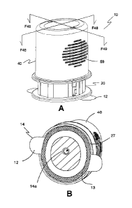
applicator 10. Figure 1B is a bottom perspective view of applicator 10 showing
a
single-sided adhesive pad 14 with an adhesive pad cover 12. As shown, the
adhesive pad cover 12 is clear only for the purpose of showing the location of
an
adhesive layer 13, but adhesive pad cover 12 may be opaque. As illustrated, an
adhesive layer 13 of adhesive pad 14 aligns with an external housing flange
portion 27 of applicator housing 21 and an adhesive pad opening 14a that
aligns
with a needle axis L2 (shown in Figs. 32-33). The non-adhesive side of the
single-sided adhesive pad 14 is bonded to lower housing bottom 172 (shown in
Fig. 22) of a sensor lower housing 170 by welding. Figures 2 and 3 are front
plan
and left side plan views of the applicator 10, respectively, showing a
vertical axis
L1 that extends through the middle of sensor applicator 10. The ready-to-use
subcutaneous sensor applicator 10 includes an applicator housing assembly 20
and a deployment button assembly 40. A unique feature of the present invention
over other similar devices is that the ready-to-use subcutaneous sensor
applicator
is fully assembled where a user does not need to combine any structural
components before use. The user simply removes the ready-to-use
subcutaneous sensor applicator 10 from its packaging, removes the adhesive
tape cover 12 from the adhesive tape 14 on the bottom of the applicator
housing
exposing the adhesive that is aligned with the proximal external body flange
portion 27, positions the subcutaneous sensor applicator in a pre-selected
location onto the user's skin or the skin of a patient, and pushes the
deployment
button assembly 40. The single push of the deployment button assembly 40
causes a sensor module 160 (not shown; see Figs. 3 and 61-62) to be deployed
onto the skin with an analyte sensor deployed subcutaneously in the skin and
the
power to the electronic circuit to be turned on automatically. The user is not
required to assemble a sensor module to the applicator, or manipulate
structure
on the applicator to remove the deployment button assembly from the sensor
22
CA 03138101 2021-10-26
WO 2020/231405
PCT/US2019/032114
module, or to perform any other task to power up the electronic circuit within
the
sensor module after subcutaneous insertion of the sensor.
[00149] Turning now to Figure 4, there is illustrated an exploded, front,
perspective view of the applicator 10. Applicator 10 includes an applicator
module 15 and an unassembled sensor module 160. The applicator module 15
includes the button deployment assembly 40, which includes a pre-loaded
insertion assembly 100, and the applicator housing assembly 20.
[00150] The pre-loaded insertion assembly 100 includes an insertion
assembly
housing 110, a needle assembly 140, a biasing element 149 and an electro-
sensor assembly 220. The needle assembly 140 and the biasing element 149
are disposed within the insertion assembly housing 110 with the biasing
element
149 compressed into a tensioned orientation such that the needle assembly 140
is in a ready or cocked position, and the insertion assembly housing 110 being
locked within the deployment button 50. The electro-sensor assembly 220 is
captured by the insertion assembly housing 110 at a lower or proximal end of
the
insertion assembly housing 110 such that a portion of sensor 250 is removably
positioned within the needle 155 of the needle assembly 140 when the needle
assembly 140 is in the ready or cocked position.
[00151] The applicator housing assembly 20 includes an applicator housing
21
and a sensor lower housing 170 captured by the applicator housing 21, which
sensor lower housing 170 is released from the applicator housing 21 when the
sensor applicator system is deployed. As shown in Figs. 1-3, the deployment
button assembly 40 is coupled to the applicator housing assembly 20 such that
a
portion of the insertion assembly housing 110 is within the applicator housing
21
and a portion of the applicator housing 21 is within the deployment button 50.
The various assembled structural components will now be described
individually.
[00152] Turning now to Figures 5-10, there is illustrated various views of
deployment button 50. Fig. 5 is a front, left-side, perspective view of
deployment
button 50. Deployment button 50 has a button elongated body 52, a closed
button distal end 53 and an optional button body flange 56 disposed at an open
button proximal end 54. The button elongated body 52 has a circumferential
wall
57 that defines a button chamber 58. Fig. 6 is a front plan view of the
deployment
button of Fig. 5. As can be seen from Figs. 5-10, button elongated body 52 has
a
23
CA 03138101 2021-10-26
WO 2020/231405
PCT/US2019/032114
length BL that is longer than a width BW. The length BL is about 1.5 inches
(3.8
cm) but this dimension is not limiting. The width BW is about 1.25 inches (3.2
cm) but this dimension is not limiting. The button chamber has a depth BD of
about 1.4 inches (3.5 cm) but this dimension is not limiting. As shown in
Figs. 5-6
and 8, the sides of button elongated body 52 may include ridges or grooves 59
to
provide better gripping of the deployment button 50 by the fingers and thumb
of
the user when placing on the skin of the user/patient.
[00153] Fig. 7 is a cross-sectional view of the deployment button of Fig. 5
taken
along line F7-F7. Within button chamber 58, a plurality of optional elongated
spacers 70 extend a predefined distance from closed button distal end 53
toward
open button proximal end 54. Also within button chamber 58, there is an
optional
spacer wall 72 that extends a predefined distance from closed button distal
end
53 toward open button proximal end 54 along the inside of circumferential wall
57.
Spacer wall 72 is located within button chamber 58 such that a space is
created
between the plurality of elongated spacers 70 and spacer wall 72, which this
space is only provided for ease of assembly during manufacturing.
[00154] Fig. 8 is a cross-sectional view of the deployment button of Fig. 5
taken
along line F8-F8. In addition to the plurality of optional elongated spacers
70 and
the optional spacer wall 72 are at least a pair of outward-facing button
retaining
arms 60. Button retaining arms 60 are connected to closed button distal end 53
and extend within button chamber 58 a predefined distance in the space created
between the plurality of elongated spacers 70 and spacer wall 72. Button
retaining arms 60 are resilient such that they can be bent toward a center of
the
button chamber 58 and return back to their original position. At the retaining
arm's end is a button retaining arm hook structure 61. As shown in Figs. 7 and
8,
closed button distal end 53 has an optional recess 53a in an outside surface
for
placement of an index finger, if so desired, when activating the subcutaneous
analyte sensor applicator system 10.
[00155] Fig. 9 is a top view of deployment button 50. In this view, a pair
of
optional closed end ports 53b is illustrated and looking down through the
optional
closed end ports 53b, one can see the hook structure 61 of the button
retaining
arms 60. The openings 53b are a result of the molds used when injection
molding the part.
24
CA 03138101 2021-10-26
WO 2020/231405
PCT/US2019/032114
[00156] Fig. 10 is a bottom view of deployment button 50. In this view, the
relationship of the plurality of elongated spacers 70 and spacer wall 72 is
more
clearly shown including the button retaining arms 60 and the optional button
flange 56.
[00157] Turning now to Figures 11-16, the structure of the applicator
housing 21
will now be discussed. Fig. 11 is a front, left-side, perspective view of
applicator
housing 21 and Fig. 12 is a front plan view of applicator housing 21.
Application
housing 21 has an applicator elongated body 22 formed by an applicator
circumferential wall 25 that defines an applicator housing chamber 28, an open
distal body end 23, an open proximal body end 24, a proximal internal body
flange portion 26 (shown in Fig 15), and a proximal external body flange
portion
27. The proximal external body flange portion 27 is an important feature of
the
applicator 10. The purpose of the flange is that it passively applies solid
even
pressure on the adhesive tape using the deployment force of the mechanism.
The resultant force of the 3-5 lbs. of deployment force is intentionally used
to
solidly set the pressure sensitive adhesive (PSA) of the adhesive tape on the
skin
of the user/patient. This is an important aspect of the present invention that
achieves the entire integrated passiveness of the mechanism for the user. The
user does not have to apply pressure to the adhesive tape to secure it to the
skin
of the user/patient after the sensor and applicator are simultaneously
inserted and
released, respectively. Applicator housing 21 also includes an inwardly-facing
applicator housing retaining arms 30 formed in the applicator circumferential
wall
25 where the applicator housing retaining arm 30 extend at a predefined angle
from the applicator circumferential wall 25 into the applicator housing
chamber 28
and terminate adjacent the open proximal body end 24. Applicator housing
retaining arm 30 is sufficiently resilient so that the arm 30 can be forced
back
toward the circumferential wall 25. A plurality of spacer slots 39 extend from
open
distal body end 23 of the applicator elongate body 22 a predefined distance
sufficient to accommodate the plurality of elongated spacers 70 of the
deployment
button 50.
[00158] Fig. 13 is a cross-sectional view of the applicator housing of Fig.
11
taken along line F13-F13. Besides the inward-facing applicator housing
retaining
arm 30, there are two other features along the inside surface of the
applicator
CA 03138101 2021-10-26
WO 2020/231405
PCT/US2019/032114
circumferential wall 25. These features include an elongated cam wall surface
32
and an applicator assembly housing stop 38. Fig. 13A is an enlarged view of
the
cam wall surface 32 delineated by area Fl 3A. As can be seen, an upper surface
portion 32a has as a first surface portion recess 33, a first sloping surface
34a
that extends along the cam wall surface 32 away from surface portion recess 33
and slopes toward the applicator housing chamber 28, a second sloping surface
34b that extends along cam wall surface 32 away from first sloping surface 34a
and slopes away from the applicator housing chamber 28. A cam surface 36
extends along middle surface portion 32b and away from second sloping surface
34a and slopes further away from the applicator housing chamber 28 where cam
surface 36 terminates at a lower surface portion 32c that has a second surface
portion recess 35. Fig. 13B is an enlarged view of the insertion assembly
housing
stop 38 delineated by area Fl 3B. Insertion assembly housing stop 38 is
located
to create an endpoint for the movement of deployment housing assembly 40
when deployment button 50 is activated. Fig. 14 is a cross-sectional view of
applicator housing of Fig. 11 taken along line F14-F14. This view illustrates
the
inward-facing applicator housing retaining arms 30 with their retaining arm
hook
ends 30a and shows the retaining arms 30 as they extend at a predefined angle
toward open proximal body end 24.
[00159] Fig. 15 is a top view of applicator housing 21. This view shows the
retaining arm hook ends 30a as well as the proximal internal body flange
portion
26. In Fig. 16, proximal internal body flange portion 26 has a flange portion
recess
26a. This recess is designed to accommodate the sensor lower housing 200 for
the purpose of presenting coplanar surfaces between open proximal body end 24
and sensor lower housing 200 while inward-facing applicator housing retaining
arms 30 hold sensor lower housing 200 until the subcutaneous analyte sensor
applicator system is deployed.
[00160] Turning now to Figures 17-22, there is illustrated various views of
one
embodiment of sensor lower housing 170. Figs. 17 and 18 are a front, left,
perspective view and a front plan view of sensor lower housing 170,
respectively.
Sensor lower housing 170 has a lower housing bottom 172, a lower housing wall
173 that extends upward from lower housing bottom 172 defining a lower housing
chamber 184, and a circumferential bottom flange 171 that extends
26
CA 03138101 2021-10-26
WO 2020/231405
PCT/US2019/032114
perpendicularly away from lower housing wall 173. In at least two, opposed
locations in lower housing wall 173, there is a lower housing locking element
174
that is inwardly facing and used to retain sensor upper housing 200 and
electro-
sensor assembly 220 after deployment of the applicator system 10. Also in at
least two, opposed locations in lower housing wall 173, there is a lower
housing
retainer recess 178 for receiving applicator housing retaining arm 30 for
holding
sensor lower housing 170 at open proximal body end 24 of applicator housing 21
prior to deployment of the applicator system 10. Also shown are a plurality of
optional flange notches 182 in circumferential bottom flange 171, which are
not
required, and used only for ease of assembly of sensor lower housing 170 to
applicator housing 21 and is not an essential aspect of the present invention.
Extending into lower housing chamber 184 from lower housing bottom 172 is a
power actuator 175 that contacts a power switch on the electro-sensor assembly
220 when sensor upper and lower housings 170, 200 are joined together when
the sensor applicator system 10 is deployed. In this embodiment, power
actuator
175 is resilient such that it has a bowed cross-sectional shape from lower
housing
bottom 172 into lower housing chamber 184. This is shown in Fig. 20A. The
bowed shape provides a biasing tension by the power actuator 175 to the power
switch 240 (shown in Fig. 44) on electronic circuit 230 when the sensor
applicator
system is deployed such that the joining of sensor upper and lower housings
170,
200 causes the power switch 240 to depress power activator 175, which, in
turn,
maintains a biasing force against power switch 240.
[00161] Figs. 19 and 20 are a cross-sectional view of sensor lower housing
170
of Fig. 17 taken along line F19-F19 and a cross-sectional view of sensor lower
housing 170 of Fig. 17 taken along line F20-F20. These views provide a more
clear view of the inwardly-facing lower housing locking elements 174, the
lower
housing retaining recess 178 and the power actuator 175.
[00162] Figs. 21 and 22 are a top plan view and a bottom plan view of lower
sensor housing 170, respectively. In this embodiment, there are three openings
176 references as vent openings 176a, 176b and sensor opening 176c. Sensor
opening 176c is for accommodating the subcutaneous sensor 250 when the
sensor applicator system is deployed. Openings 176a and 176b are optional and
27
CA 03138101 2021-10-26
WO 2020/231405
PCT/US2019/032114
may provide ventilation to the patient's skin to allow trapped moisture to
wick out
of the sensor housing 170.
[00163] Turning now to Figures 23-29, there are illustrated various views
of one
embodiment of the insertion assembly housing 110. Figs. 23 and 24 are a front
perspective view and a front plan view of the insertion assembly housing 110.
Insertion assembly housing 110 includes an assembly housing body 112, an open
housing distal end 113, a closed housing proximal end 114, an assembly housing
bottom 115, and an assembly circumferential wall 111 defining an assembly
housing chamber 118. Assembly circumferential wall 111 includes an assembly
housing locking slot 130 spaced from open housing distal end 113 that receives
outwardly facing button retaining arm 60 when insertion assembly housing 110
is
assembled into deployment button 50. Once insertion assembly housing 110 is
inserted and retained within deployment button 50, it remains locked within
deployment button 50 and always moves with the deployment button 50.
[00164] Assembly circumferential wall 111 also includes a plurality of
assembly
housing retaining arms 120 where each of the retaining arms 120 have an
outward-facing housing arm hook surface 121. The retaining arms 120 reside in
first surface portion recess 33 of the elongated cam wall surface 32 and lock
insertion assembly housing 110 within applicator housing 21, which effectively
locks deployment button 50 to applicator housing 21 by way of the button
retaining arms 60 of deployment button 50 being locked into assembly housing
locking slot 130 of the assembly circumferential wall 111 of insertion
assembly
housing 110. During deployment of the sensor applicator system, each assembly
housing retaining arm 120 slides along the elongated cam wall surface from the
first surface portion recess 33 when in the ready-to-use orientation to the
second
surface portion recess 35 when in the deployed orientation.
[00165] Another aspect of assembly circumferential wall 111 includes a
plurality of housing retaining fingers 124 where each retaining finger 124 has
an
inward-facing finger hook surface 125. Each retaining finger 124 extends below
assembly housing bottom 115 and holds sensor upper housing 200 when the
sensor applicator system 10 is in the ready-to-use orientation.
Circumferential
wall 111 also includes a needle assembly locking slot 132 that extends a
predefined distance from closed housing proximal end 114 toward open housing
28
CA 03138101 2021-10-26
WO 2020/231405
PCT/US2019/032114
distal end 113. Needle assembly locking slot 132 is to accommodate the
applicator assembly housing stop 38 of applicator housing 21, which will
interact
with needle assembly 140 (to be discussed later) when sensor applicator system
is deployed to insert subcutaneous sensor 250.
[00166] Turning now to Figs. 25 and 26, there are illustrated a cross-
sectional
view of insertional assembly housing 110 taken along ling F25-F25 and F26-F26,
respectively. As shown in these figures, assembly housing bottom 115 is
recessed to accommodate sensor upper housing 200 while the plurality of
housing retaining fingers 124 hold sensor upper housing 200 within the
recessed
housing bottom 115 until released by activation of the sensor applicator
system
10.
[00167] Figs. 27 and 28 illustrate a top view and a bottom view of
insertion
assembly housing 110. In these views, it is clearly shown that outward-facing
housing arm hook surface 121 of assembly housing retaining arm 120 extend
beyond the perimeter of assembly circumferential wall 111 for engagement with
elongated cam wall surface 32 of applicator housing 21 and the existence of a
housing proximal end opening 116 to accommodate the needle 155 of the needle
assembly 140. Also shown is at least one optional assembly housing rail 117
that
also extends along a major portion of assembly circumferential wall 111
between
open housing distal end 113 and closed housing proximal end 114, and beyond
the perimeter of assembly circumferential wall 111. This optional rail 117, if
included, would be disposed within a corresponding applicator housing channel
29 to facilitate alignment of insertion assembly housing 110 within applicator
housing 21. Fig. 29 is a bottom perspective view of the insertion assembly
housing 110 to provide a visual of the structural relationship of the assembly
housing bottom 115, the assembly housing retaining arm 120, the housing
retaining finger 124, and needle assembly locking slot 132.
[00168] Turning now to Figures 30-35, there is illustrated various views of
one
embodiment of a needle assembly 140. Figs. 30 and 31 are a front perspective
view and a front plan view of needle assembly 140. Needle assembly 140
includes a needle body 142 and a tubular needle 155 with a needle wall 155a
(not
shown) fixedly attached to needle body 142 where the tubular needle 155
defines
a needle axis L2 (shown in Figs. 32, 32).
29
CA 03138101 2021-10-26
WO 2020/231405
PCT/US2019/032114
[00169] Figs. 32 and 33 illustrate a cross-sectional view of the needle
assembly
of Fig. 30 taken along line 32-32 and a cross-sectional view of the needle
assembly of Fig. 30 taken along line 33-33, respectively. Needle 155 is
located to
align with housing proximal end opening 116 of insertion assembly housing 110.
Needle body 142 has a closed needle body distal end 143, an open needle body
proximal end 144, a needle body top 145, a needle body retaining arm 150, and
a
needle-receiving portion 154. Needle 155 has a needle wall 155a that forms a
needle body 156 with a needle distal end 157 and a needle proximal end 158.
Needle distal end 157 is fixedly secured to needle-receiving portion 154 of
needle
body 142. More specifically, the needle is fixated to the needie-receiving
portion
154 with tight toierance. A usable securing material is UV epoxy. This
fixation is
important because the portion of the needle wail that's removed must align
closely with sensor 250. Needle proximal end 158 includes a needle sharp 159.
Needle 155 includes a needle open region 156a where a portion of the needle
wall 155a is removed. Needle open region 156a extends from needle proximal
end 158 for a predefined distance. Needle open region 156a is needed to
accommodate sensor 150 and to allow retraction of needle 155 after deployment
of sensor 150 subcutaneously. Fig. 32 shows the structure of needle body
retaining arm 150 where retaining arm 150 has an outward-facing needle
retaining arm hook surface 151 that extends beyond the needle body
circumferential wall 141 when needle body retaining arm 150 is in a relaxed
state.
Needle body retaining arm 150 is resilient and configured such that it may be
compressed toward and into needle body circumferential wall 141. Fig. 33 shows
one embodiment of needle receiving portion 154 of needle body 142. Needle
receiving portion 154 is configured to delineate an area around which biasing
element 149 resides between closed needle body distal end 143 and closed
housing proximal end 114 of the insertion assembly housing 110. When needle
assembly 140 is assembled inside of assembly housing chamber 118 of the
insertion assembly housing 110, biasing element 149 is in a compressed state
and needle body retaining arm 150 is located within and held by needle
assembly
locking slot 132 of insertion assembly housing 110 until released by
interference
with applicator assembly housing stop 38 of applicator housing 21 when
deployment button assembly 40 is deployed to insert sensor 250 subcutaneously.
CA 03138101 2021-10-26
WO 2020/231405
PCT/US2019/032114
When applicator assembly housing stop 38 forces needle body retaining arm 150
into needle body 142, biasing element 149 moves to a less compressed state
causing needle assembly 140 to slide toward open housing distal end 113
causing needle 155 to retract away from upper sensor housing 200.
[00170] Figs. 34 and 35 are a top view and a bottom view of needle assembly
140. These views show the position of the needle body retaining arm 150
relative
to the needle body 142. Also shown are needle body side slots 146 that are
included for two reasons: (a) to prevent any inadvertent disconnection of
outwardly-facing button retaining arm 60 of the deployment button 50 from the
assembly housing locking slot 130 and (b) to prevent possible interference
with
needle body 142 as it slides up toward deployment button top 55 after
implanting
sensor 250 into subcutaneous tissue. In the bottom view, an outline 149a of
the
biasing element 149 is provided to show the relative position of the biasing
element 149 against the inside top surface of the needle body top 145.
[00171] Turning now to Figures 36 and 37, there is illustrated a front,
top,
perspective view and a rear, bottom, perspective view of one embodiment of a
sensor upper housing 200 containing an electro-sensor assembly 220. The
electro-sensor assembly 220 includes an electronic circuit 230 and a sensor
250.
Fig. 36 shows a subcutaneous sensor 250 extending a predefined distance
below sensor upper housing 200. Fig. 37 shows electro-sensor assembly 220
residing within sensor upper housing 200. After the electro-sensor assembly
220
is assembled within sensor upper housing 200, a potting compound 215 is
applied by an automatic dispensing machine (not shown) to the sensor upper
housing 200. The potting compound 215 seeps down under the electronic circuit
230 and is filled until the potting compound 215 is just even with the base of
the
activation switch 240 (shown in Fig. 44) and flows out to the inner
circumference
to the sensor upper housing 200 and the electronic circuit retainer 209. The
potting compound is typically a waterproof material, preferably a 2-part fast-
curing
material. Fig. 36A is an exploded view of Fig. 36 showing electro-sensor
assembly 220 and sensor upper housing 200.
[00172] Figs. 38, 38A and 39 are a front, perspective view, an enlarged
view of
an upper housing retaining recess and a front plan view, respectively, of
sensor
upper housing 200. Sensor upper housing 200 has an upper housing top 205, an
31
CA 03138101 2021-10-26
WO 2020/231405
PCT/US2019/032114
upper housing top opening 206, a circumferential upper housing wall 207 that
extends transversely away from upper housing top 205 and defines an upper
housing chamber 212 (shown in Figs. 40, 41), and a housing top flange portion
208 that extends from upper housing top 205 transversely beyond
circumferential
upper housing wall 207. Circumferential upper housing wall 207 also includes
an
upper housing locking recess 210 adjacent housing top flange portion 208.
Upper
housing locking recess 210 is located for locking engagement with a
corresponding lower housing locking element 174 when joined together to form
sensor module 160 is deployed on a user's skin. On the inside of
circumferential
upper housing wall 207 is at least one electronic circuit retainer 209 that
holds the
electronic circuit 230 within upper housing chamber 212.
[00173] Figs. 40 and 41 are a cross-sectional view of the sensor upper
housing
of Fig. 38 taken along line F40-F40 and a cross-sectional view of the sensor
upper housing of Fig. 38 taken along line F41-F41, respectively. Descending
from upper housing top opening 206 is a tubular upper housing needle guide
211.
Upper housing needle guide 211 has a guide distal end 211a and a guide
proximal end 211b. Furthermore, the needle guide 211 extends a predefined
distance such that, when sensor upper housing 200 is coupled with sensor lower
housing 170, guide proximal end 211b of upper housing needle guide 211
extends no further than lower housing bottom 172. Guide proximal end 211b has
a portion 211c removed to accommodate sensor 250, which has a bend that is
positioned within portion 211c and where a portion of sensor 250 is positioned
within the needle open region of needle 155. Fig. 41 is a cross-sectional view
of
the sensor upper housing of Fig. 38 taken along line F41-F41 showing the upper
housing locking recess 210.
[00174] Turning now to Figs. 42 and 43, there is illustrated the electronic
circuit
230 without sensor 250. Fig. 42 is a bottom perspective view and Fig. 43 is a
top
perspective view. Fig. 43 clearly shows the battery 235 that powers electronic
circuit 230. Fig. 42 shows a circuit power switch 240 that is in a normally
off
position. Fig. 44 is an enlarge view area F44 delineated in Fig. 42. Circuit
power
switch 240 is a frusto-conical shape above adjacent electronic components of
the
electronic circuit 230. Circuit power switch 240 is positioned on electronic
circuit
230 to couple with the power actuator 175 of sensor lower housing 170 when
32
CA 03138101 2021-10-26
WO 2020/231405
PCT/US2019/032114
sensor upper housing 200 and sensor lower housing 170 are coupled together
during sensor applicator system activation and deployment. When coupled
together, power actuator 175 pushes against circuit power switch 240 which
then
connects power from battery 232 to electronic circuit 230 and sensor 250. The
sensor module 160 is automatically powered on when this action occurs. In
other
words, this action automatically occurs when the sensor applicator system 10
is
deployed and the sensor module 160 deployed on the skin of the user with the
sensor implanted subcutaneously. Electronic circuit 230 also includes
electronic
components such as, for example, a transmitter (not shown) for wireless
communication of sensor and other data with an electronic device 902 such as
those devices described later.
[00175] Figs. 45 and 46 are front and rear views of one embodiment of
sensor
250, respectively. Sensor 250 has a sensor distal end 260, a sensor middle
portion 270 and a sensor proximal portion 280. Sensor distal end 260 has a
plurality of contact pads 262 that electrically couples to electronic circuit
230.
Sensor proximal portion 280 along with a portion of sensor middle portion 270
is
implanted subcutaneously within the skin of the user/patient. A plurality of
electrodes 282 are exposed at sensor proximal portion 280 where at least one
of
the plurality of electrodes 282 is configured to measure an analyte, such as,
for
example, glucose. More than one analyte may be measured provided that other
of the plurality of electrodes 282 are so configured. In this embodiment,
sensor
250 has a bend such that sensor proximal portion 280 is transverse, and
preferably perpendicular, to sensor distal end 260.
[00176] Fig. 47 is an enlarged, rear view of sensor 250 showing sensor
proximal
portion 280 and the plurality of electrodes 282 with sensor distal portion 260
extending away from the viewer and into the plane of the drawing. As seen,
this
embodiment of sensor 250 has one or more friction surfaces 284 that appear as
bumps along the side of sensor proximal portion 280. These "bumps" contact the
inside surface of needle wall 155a in needle open region 156a. The frictional
contact between sensor proximal portion 280, needle wall 155a and the size of
sensor 250 allow needle 155 to penetrate the skin of the user and implant
sensor
proximal portion 280 subcutaneously without damaging sensor proximal portion
33
CA 03138101 2021-10-26
WO 2020/231405
PCT/US2019/032114
280 or any portion of sensor 250 and then withdraw needle 155 leaving sensor
proximal portion 280 implanted.
[00177] Turning now to Figures 48-62, there will be discussed the operation
of
the all-inclusive, ready-to-use sensor applicator system 10. Figs. 48 and 49
are
cross-sectional views of the applicator system 10 in a ready-to-use state.
Fig. 48
is a left-side, cross-sectional view of the applicator system 10 of Fig. 1
taken
along line F48-F48 in Fig. 1 showing the applicator system is a ready-to-use
state.
As illustrated, sensor applicator system 10 is packaged as ready-to-use and is
all-inclusive, meaning that the user does not need to assemble a "sensor
module"
to an inserter or to physically connect a power source to the sensor module to
operate the sensor module (i.e. to power the electronic circuit and sensor).
In this
all-inclusive, ready-to-use position, the needle assembly 140 is coupled
inside of
the insertion assembly housing 110 with the biasing element 149 in a
compressed
state storing potential energy used for retracting the needle 155 once
deployed.
The sensor upper housing 200 is retained at the closed housing proximal end
114
of the insertion assembly housing 110. Needle 155 extends through upper
housing needle guide 211 toward sensor lower housing 170 where needle
proximal end 158 is position directly aligned with and adjacent the sensor
opening
176c of sensor lower housing 170. Fig. 49 is a front, cross-sectional view of
the
applicator system of Fig. 1 taken along line F49-F49 in Fig. 1. This view
shows
outwardly-facing button retaining arms of deployment button 50 engaged in
assembly housing locking slot 130 of insertion assembly housing 110. This is
more clearly shown in Fig. 50A, which is an enlarged view within the area
delineated by F50A in Fig. 549. This view also shows inwardly-facing
applicator
housing retaining arm 30 coupled to lower housing locking recess 178 to retain
sensor lower housing 170 to application housing 21. This is more clearly shown
in Fig. 50B, which is an enlarged view within the area delineated by F5OB in
Fig.
49.
[00178] Figs. 51 and 53 are cross-sectional views of the applicator system
10 in
a deployed orientation just before completion of the implantation of sensor
250
before needle 155 is retracted and the sensor upper and lower housings 170,
200
are joined to each other. The purpose is to show the spatial relationship of
the
relevant retaining arms and corresponding locking recesses of the various
34
CA 03138101 2021-10-26
WO 2020/231405
PCT/US2019/032114
components where substantially simultaneously, the sensor module 160 is about
to be completed, the needle 155 and sensor 250 are within the subcutaneous
tissue of the user, the needle assembly 140 is about to be automatically
retracted,
and the sensor module 160 is about to be released from the applicator housing
21. Fig. 51 a left-side, cross-sectional view of the applicator system of Fig.
48
showing the applicator system partially deployed just short of full
deployment.
Fig. 52 is an enlarged view within the area delineated by F52 in Fig. 51
showing
that the needle body retaining arm 150 is about to make contact with
applicator
assembly housing stop 38. Fig. 53 is a front, cross-sectional view of the
application system of Fig. 51 showing the closed housing proximal end 114 of
the
insertion assembly housing 110 about to make contact with the inwardly-facing
applicator housing retaining arm 30. Fig. 54 is an enlarged view within the
area
delineated by F54 in Fig. 53.
[00179] Figures 55 and 57 are cross-sectional views of the applicator
system 10
in a deployed orientation upon completion of the implantation of sensor 250.
Fig.
55 is a left-side, cross-sectional view of the applicator system of Fig. 48
showing
the applicator system 10 fully deployed with the needle assembly 140 retracted
within the insertion assembly housing 110. As shown, sensor upper housing 170
is coupled with sensor lower housing 200 and needle assembly 140 has been
moved by the kinetic energy of released biasing element 149 where the needle
body top 145 is in contact with deployment button top 55. Fig. 56 is an
enlarged
view within the area delineated by F56 in Fig. 55. Fig. 55 more clearly shows
the
contact between needle body top 145 and deployment button top 55. Fig. 57 is a
front, cross-sectional view of the applicator system 10 of Fig. 55 fully
deployed. In
this view, closed housing proximal end 114 had made contact with inwardly-
facing
applicator housing retaining arm 30 and, at its furthest most travel, has
completely
pushed retaining arm 30 away from sensor lower housing 170, which releases the
now formed sensor module 160 from the applicator module 15. Fig. 58 is an
enlarged view within the area delineated by F58 in Fig. 57 to more clearly
show
how the retaining arm 30 is released from sensor lower housing 170.
[00180] Turning now to Figures 59 and 60 are cross-sectional views of the
ready-to-use orientation and the fully deployed orientation of the assembly
housing retaining arm 120 and the elongated cam wall surface 32 of the
CA 03138101 2021-10-26
WO 2020/231405
PCT/US2019/032114
applicator housing 21. At the ready-to-use orientation, a sufficient force
against
the deployment button 50 is required to overcome the resistance created by the
first sloping surface 34a of the cam wall surface 32, which sloping surface
34a
causes the assembly housing retaining arm 120 to push and bias the arm 120
toward the assembly housing chamber 118 (i.e. by riding/sliding along sloping
surface 34a) until the assembly housing retaining arm 120 reaches second
sloping surface 34b of the cam wall surface 32. The initial force applied
against
the deployment button 50 coupled with the force of the biased arm 120 causes
the deployment button to continue to move without additional force required to
its
fully deployed position as the assembly housing retaining arm 120 follows
along
the second sloping surface 34b and the cam surface 36 which continues to slope
away (i.e. outwardly) applicator housing chamber 28 until assembly housing
retaining arm 120 reaches second surface portion recess 35 of the elongated
cam
wall surface 32. At this point downward movement of deployment button
assembly 40 ceases since the sensor module 160 is fully deployed.
[00181] Figs. 61 and 62 are a right-side plan view and a front plan view of
the
fully deployed sensor applicator system 10 showing the sensor module 160
deployed and separated from the applicator module 15 with sensor 250 deployed
subcutaneously within the skin of the user/patient.
[00182] Needle/sharp
[00183] Figures 63 and 64 illustrate perspective views of one embodiment of
a
needle/sharp 300 of the present invention. Needle/sharp 300 includes a sharp
body 302, a sharp open region 304, and a sharp tip 306. Sharp body 302 is an
annular section of sharp 300 that extends longitudinally and defines an
enclosed
conduit 301 therethrough.
[00184] A wire EDM machining operation or a laser operation is used to remove
a portion of the tubing wall 303 along sharp 300 a predefined distance to
define
sharp open region 304, thereby reducing the overall height 310 of sharp 300.
Both the wire EDM machining operation and the laser operation can be performed
on cylindrical tubing or on flattened, oval tubing. Sharp open region 304 is a
section of an annulus that extends longitudinally with the tubing wall 303
along the
length of sharp open region 304 defining an unenclosed concave well 314 from
36
CA 03138101 2021-10-26
WO 2020/231405
PCT/US2019/032114
sharp tip 306 to sharp body 302. Concave well 214 is sized to receive a
continuous monitoring sensor 250.
[00185] CGM System
[00186] Referring now to Figs. 65 and 66, there is illustrated one
embodiment of
the CGM system 1000 of the present invention. CGM system 1000 includes
subcutaneous analyte sensor applicator 10, and an electronic device 900, 902
that is equipped for wireless communication. An adhesive pad 14, which is
welded only to a bottom of the sensor lower housing 170 also has an adhesive
layer on an opposite side of the adhesive pad 14 where the adhesive layer
coincides with the bottom of proximal external body flange portion 27 of
applicator
housing 21 for adhesively attaching the applicator module 15 to the skin of a
patient. This is shown in Fig. 1 B.
[00187] Figure 66 shows one embodiment of system 1000 in use after
insertion
of sensor 250 into the subcutaneous tissue. As shown, Fig. 66 shows examples
of electronic device 902, 902', a transmitter 1004 (which is sensor module 160
containing sensor lower housing 170, sensor upper housing 200 and electro-
sensor assembly 220) on the patient's arm, where transmitter 1004
communicates analyte measurement data from continuous monitoring sensor 250
(deployed subcutaneously into the patient) to electronic device 902, where the
data is displayed to the user on a user interface 918.
[00188] System 1000 also includes system software installed on an
electronic
device 902 equipped for wireless communication with transmitter 1004.
Optionally, system 1000 utilizes an analyte strip reader 906 (not shown) for
calibration that is capable of wireless communication with electronic device
902.
Although a smartphone with software is illustrated, it is understood that the
electronic device could be a dedicated reader/meter that is the size of a
smartphone or it could be an integrated meter that includes a dedicated
continuous glucose monitoring meter integrated with a blood glucose meter for
calibration. Examples of electronic device 902 include a computer, a tablet
computer, a smartphone, a data logger, a watch, an automobile
information/entertainment system, or other electronic device. Wireless
communication may be via radio frequency (RF) communication, Wi-Fi,
37
CA 03138101 2021-10-26
WO 2020/231405
PCT/US2019/032114
BlueTooth, near-field communication (NFC), a sensor radio, mobile body area
networks (MBAN) or other wireless communication protocol. In the embodiment
employing a strip reader 906, strip reader 906 has integrated BLE (BlueTooth
low
energy) and will send calibration data wirelessly to electronic device 902 and
query the patient regarding the patient's intention to use the new calibration
data
point.
[00189] In one embodiment, transmitter 1004 communicates to the electronic
device 902 using a wireless personal area network (WPAN), such as Bluetooth
Low Energy (BLE). In other embodiments, other wireless communication
protocols may be used with communication generally effective within a range of
a
few centimeters to a few meters. In some embodiments, for example, the system
software is configured to communicate with Android and/or Apple software
platforms installed on mobile phones and the like and has a range of up to
thirty
feet (about 9.2 meters).
[00190] In one embodiment, transmitter 1004 is designed to conserve power
and operates via standard Bluetooth BLE protocol. For example, sensor readings
from continuous monitoring sensor 250 are transmitted from transmitter 1004
every five minutes and the sensor reading is promptly displayed to the user
after
being received by the user's electronic device 902. Typically, transmitter
1004 will
successfully connect with the electronic device 902 after one or two attempts.
[00191] In one embodiment, system 1000 uses universally unique identifier
(UUID) filtering to prevent unwanted communication from another device. It is
expected that multiple devices may be present and discoverable in proximity to
electronic device 902, particularly when the user is in a densely populated
area as
in a subway, concerts, or other public locations.
[00192] In one embodiment, system 1000 utilizes calibration data obtained
wirelessly from a separate strip reader. For example, a finger strip reading
for
glucose is taken and then either manually or automatically entered in system
1000 for calibration. In one embodiment, the system 1000 software application
has a means for the user to manually enter a one-point calibration value taken
from any meter. For example, the user uses the interface of the electronic
device
902 to enter a calibration reading of 100 mg/di obtained using a separate
strip
reader. After entering the calibration data, the user can accept, reject, or
38
CA 03138101 2021-10-26
WO 2020/231405
PCT/US2019/032114
manually re-enter the calibration data. In other embodiments, the system
software receives BLE calibration information from the external meter. After
system 1000 receives the calibration data, the user can accept, reject, or
manually re-enter this calibration data into the user interface.
[00193] The system software provides a user interface 918, one example of
which is a touch-sensitive display screen. In one embodiment, user interface
918
has a main screen 909 with indicators 910a for radio strength and battery
strength. Another indicator 910b displays the analyte concentration (e.g.,
glucose
concentration) in units of mg/dL (milligrams per deciliter) or mmol/L
(millimoles per
liter). Indicator 910c displays a glucose trending arrow to communicate to the
user whether the analyte concentration (e.g., glucose) is increasing,
decreasing,
or unchanged. In one embodiment, indicator 910c for the trending arrow also
communicates the relative rate of change.
[00194] In one embodiment, for example, a rate of change having an absolute
value equal to or greater than a predefined value (e.g., 3 mg/dL / minute) is
displayed as two vertically-oriented arrows (up or down); a rate of change in
a
second predefined range with an absolute value less than the predefined value
(e.g., 2-3 mg/dL / minute is displayed as a single vertically-oriented arrow
(up or
down); a rate of change in a third predefined range with absolute value less
than
the second predefined range (e.g., 1-2 mg/dL / minute is displayed as an arrow
inclined at 45 to the horizontal (up or down); and a rate of change in a
fourth
predefined range with an absolute value less than the absolute value of the
third
predefined range (e.g., 1 mg/dL / minute or less) is displayed as a horizontal
arrow to indicate a steady state. In one embodiment, the rate of change is
calculated based on five consecutive data points using the following formula:
[00195] In one embodiment, analyte (e.g., glucose) concentration is updated
every one minutes with data from transmitter 1004 and displayed on main screen
909. Optionally, transmitted data is updated and stored in transmitter 1004 in
case electronic device 902 is out of range or unable to receive during that
period.
In one embodiment, each transmission by transmitter 1004 includes a predefined
39
CA 03138101 2021-10-26
WO 2020/231405
PCT/US2019/032114
number of previous data points (e.g., five) to fill in missing data in the
event
electronic device 902 is unable to receive during that period.
[00196] Main screen 909 also displays a plot 911 of analyte concentration
versus time. In one embodiment, the Y-axis (analyte concentration) is
configured
to automatically scale with a minimum Y-axis value 10% below the minimum
value of plotted data and the maximum Y-axis value 10% above the maximum
value of plotted data. The X axis may be configured to display a timeframe of
the
user's choosing.
[00197] Main screen 909 also displays a macro timescale 912 of data that
includes data displayed in plot 911. Part of the data displayed in macro
timescale
912 is highlighted and corresponds to the data displayed in plot 911. For
example, macro timescale 912 may be configured to display analyte
concentration data over three hours, six hours, twelve hours, twenty-four
hours,
three days, or one week. Accordingly, data displayed in plot 911 is a subset
of
data displayed in macro timescale 912. In one embodiment, highlighted area 913
of macro timescale 912 is an active element on user interface 908. For
example,
by touching highlighted area 913 in the center and dragging left or right, the
data
of plot 911 is selected and moved. Similarly, by touching highlighted area 913
on
left edge 913a or right edge 913b and dragging left or right, highlighted area
913
is expanded or contracted along the time axis. When the size or location of
highlighted area 913 is adjusted, plot 911 is automatically updated to display
data
between the same minimum time and maximum time of highlighted area 913.
Main screen 909 also displays an active service icon 915. Selecting active
service icon 915 displays a service screen with indicators 910 for calibration
and
customization. For example, the service screen includes indicators 910 for
setting
upper and lower ranges, alarm limits, displayed units, device pairing
settings, time
scale, X-axis time domain, and the like. For example, the user accesses the
service screen to set the time range of data displayed in macro timescale 912
and
plot 911. Selecting the calibration icon opens a calibration screen used to
calibrate analyte data. In some embodiments, the service screen includes
instructions for use or a link to access instructions for use.
[00198] For example, user-set or default values for maximum and minimum
concentration/control limits are displayed on plot 911 as dashed lines 916a,
916b,
CA 03138101 2021-10-26
WO 2020/231405
PCT/US2019/032114
respectively, extending horizontally. In one embodiment, user-set control
limits
are not alarmed. Default control limits provide upper and lower alert limits
and
upper and lower reportable range limits. A reading above the maximum 916a or
below the minimum 916b results in an alarm, such as vibration or an audible
alert
to the user. In one embodiment, maximum concentration limit 916a has a default
value of 510 mg/dL and minimum concentration limit 916b has a default value of
90 mg/dL.
[00199] In some embodiments, system software is configured to generate
reports for health care professionals. For example, touching an icon opens
reports and configurations that could be transferred to a Health Care
Professional
via the cloud, such as the amount of time above and below target ranges; alarm
reports, CGM values; estimated Al C and eAG values, and analyte
measurements over time.
[00200] In one embodiment, system 1000 enables the user to manually enter a
one-point calibration value taken from a separate glucose strip reader. For
example, the user enters 100 mg/dl as obtained from a test strip measurement.
After entering calibration data, the patient shall accept, reject, or manually
re-
enter this calibration data into the user interface.
[00201] In another embodiment, system 1000 is configured to receive
calibration information from strip reader via BLE or other wireless
communication
protocol.
[00202] In some embodiments, settings and preferences may be locked and are
accessed only by entering a password, biometric information, or other
information
serving as a key to unlock the settings and preferences menu.
[00203] In one embodiment, system 1000 performs general data calculations
using the following generic variable labels:
AO = (M*X + B) ¨ (N*Y +C)
Al = AO + calibration adjusment
A2 = A1/18.018018
X = ((<channel 0>*0.000494) - 1)* 1000
Y = ((<channel 1>*0.000494) - 1) * 1000
[00204] Generic variables are defined as follows:
AO is uncalibrated CGM value in mg/dL
41
CA 03138101 2021-10-26
WO 2020/231405
PCT/US2019/032114
Al is calibrated displayed CGM value in mg/dL
A2 is calibrated displayed CGM value in mmol/L (alternate units)
X is the mV reading output of Channel 0 (the sensor signal channel)
M is the slope correction factor Channel 0
B is offset correction factor for Channel 0
Y is the my reading output of Channel 1 (the blank signal channel)
N is the slope correction factor for channel 1
C is the offset correction factor for channel 1
[00205] In one embodiment, values for M, B, N, and C variables are stored
on
electronic device 902. In one embodiment, values AO, Al, X, and Y are stored
to
a Sqlite Database along with date timestamp. For example, datetime, channel-0-
value, channel-1-value, calculated-glucose value, calculated-glucose-value-
with-
calibration, and device-id. Optionally, a separate database includes patient-
entered calibration data with timestamp, such as datetime, entered-calibration
value, and device-id.
[00206] In one embodiment, values for Al or A2 (values displayed to the
patient
in plot 911) that are greater than a predefined maximum limit (e.g., 500 mg/dL
or
27.7 mmol/L) result in an error message displayed on user interface 918, such
as
"Above Reportable Range." Similarly, values for Al or A2 of less than a
predefined minimum limit (e.g., 40 gm/dL or 2.2 mmol/L) result in an error
message displayed to the user, such as "Below Reportable Range."
[00207] Communication between transmitter 1004 and electronic device 902 is
secure. For example, BLE-supported Security Manager Protocol is utilized
between transmitter 1004 and electronic device 902. SMP defines the
procedures and behavior to manage pairing, authentication, and encryption
between the devices, including encryption and authentication, pairing and
bonding, key generation for device identity resolution, data signing,
encryption,
pairing method based on the input/output capabilities of transmitter 1004 and
electronic device 902.
[00208] In one embodiment, electronic device 902 is a watch configured to
communicate wirelessly with transmitter 1004. In such an embodiment, system
software includes three screens on the user interface 918 of the electronic
device
902' configured as a watch. A first screen displays the most recent analyte
42
CA 03138101 2021-10-26
WO 2020/231405
PCT/US2019/032114
concentration and units of measurement. For example, glucose concentration is
displayed by indicator 910b in mg/dL or mmol/L and is updated every five
minutes. A trending arrow indicator 910c shows the relative rate of change as
discussed above.
[00209] A second screen displays the most recent glucose concentration and
units of measurement. Second screen displays plot 911 with analyte
concentration data for the previous one hour, where the Y-axis is glucose
concentration and the X-axis is time. Upper and lower limits 916a, 916b are
displayed in dashed lines. A third screen displays macro timescale 912 with
twenty-four hours of acquired data.
[00210] Sensor Construction
[00211] Figure 67 shows a perspective illustration of one embodiment of a
multi-layer sensor assembly 500 ready for deposition of reagents to create a
continuous monitoring sensor 250 having, in this embodiment, a reference
electrode 534, a blank or second working electrode 533, a counter electrode
532,
and a first working electrode 530. Electrodes 530, 532, 533, 534 are formed at
a
substrate distal end portion 502 and communicate electrically through assembly
middle portion 530 with electrically-conductive contact pads 503 at a
substrate
proximal end portion 501. Multi-layer sensor substrate 500 is useful to form a
subcutaneous analyte sensor, such as a glucose monitoring sensor.
[00212] A sensing layer (not shown) is formed over each of the first and
second
working electrodes 530, 533. The sensing layer is made up of three coating
layers, a base coating layer, a second coating layer and a third or top
coating
layer. The base coating layer contains poly-2-hydroxyethyl methacrylate
(PHEMA) and is the coating that is disposed directly on the exposed metal at
the
bottom of the respective wells at substrate distal end portion 502. Specific
to the
first working electrode where glucose is measured, glucose oxidase and/or
glucose dehydrogenase is also included. The second working or blank electrode
does not contain any enzyme and is used only for measuring background noise
and/or interferents in the sample since the first working electrode will have
a total
current that include a portion driven by the amount of glucose in the
subcutaneous tissue as well as the background noise and/or interefents derived
43
CA 03138101 2021-10-26
WO 2020/231405
PCT/US2019/032114
current. Using an algorithm to subtract the current derived from the second
working or blank electrode from the first working electrode provides a more
accurate glucose measurement. The second coating layer is disposed directly on
the base coating layer and contains PHEMA and a plurality of microspheres from
polydimethylsiloxane (PDMS). PDMS is a material a material having
substantially
no or little permeability to glucose but a substantially high permeability to
oxygen.
The third or top coating layer is disposed directly on the second coating
layer and
contains PHEMA and catalase. Catalase is a material that prevents release of
hydrogen peroxide from the sensing layer into the surrounding environment. In
this case, the surrounding subcutaneous tissue. For the reference electrode
534,
a silver-silver chloride (AgCI) layer is created on the metal at the bottom of
the
well and then the AgCI layer is covered with a hydrogel membrane. The counter
electrode 532 has the metal at the bottom of the well covered only with a
hydrogel
membrane.
[00213]
Referring now to Figure 68, a perspective, exploded illustration shows a
base layer 510, a middle layer 550, and a top layer 580 that together comprise
multi-layer sensor substrate 500. "Middle layer" herein means the layer
adjacent
to the top layer 580 without any intervening, electrically-insulating layer
when
there are other layers between base layer 510 and middle layer 550. Base layer
510 is electrically insulating and includes a base proximal end portion 514, a
base
distal end portion 516, and a base middle portion 518 between base proximal
end
portion 514 and base distal end portion 516. A base metallized layer 520 is
disposed on base layer 510 and defines at least one circuit 552 extending
longitudinally along base layer 510. Each circuit 552 has an electrically-
conductive contact pad 524 formed at base proximal end portion and an
electrically-conductive contact pad 526 formed at base distal end portion 516
with
an electrically-conductive trace 528 electrically coupling electrically-
conductive
contact pad 524 at the base proximal end 514 with electrically-conductive pad
526 at base distal end 516.
[00214] Middle
layer 550, also electrically insulating, is disposed over base layer
510 and includes a middle layer proximal end portion 554, a middle layer
distal
end portion 556, and a middle layer middle portion 558. Middle layer 550 has a
size and shape corresponding to base layer 520 and that is aligned with base
44
CA 03138101 2021-10-26
WO 2020/231405
PCT/US2019/032114
layer 510. Middle layer 550 includes electrically-conductive contact pads 560
at
middle layer distal end portion 556 adapted to receive an electrode material
or
reagent to form a respective electrode. Each electrically-conductive contact
pad
562 at middle layer proximal end portion 554 is adapted to receive an
electrical
contact.
[00215] The top layer 580, also electrically-insulating, is disposed over
middle
layer 550. Top layer 580 has a size and shape corresponding to middle layer
550
and base layer 510. Top layer 580 has a top layer proximal end portion 582, a
top layer distal end portion 584, and a top layer middle portion 586, where
top
layer 580 aligned with base layer 510 and middle layer 550. Top layer 580 has
a
plurality of openings that include contact openings 590 on substrate proximal
end
portion 501 and sensor wells 592 on substrate distal end portion 502. Contact
openings 590 and sensor wells 592 coincide with electrically-conductive
contact
pads 560, 562, respectively, of middle layer 550. Base layer 510, middle layer
550, and top layer 580 are manufactured with circuits 552, 572 on base layer
510
and middle layer 550 to create multi-layer sensor substrate 500 with substrate
proximal end portion 501, substrate distal end portion 502, and assembly
middle
portion 503 extending longitudinally between substrate proximal end portion
501
and substrate distal end portion 502 as shown, for example, in Fig. 42.
Substrate
distal end portion 502 and assembly middle portion 503 each have a width of
about 279 microns.
[00216] Referring now to Figures 69-71, base layer 510 is shown in a plan
view
in Fig. 44, base proximal end portion 514 is shown enlarged in Fig. 70, and
base
distal end portion 516 is shown enlarged in Fig. 71. Base layer 510 has a base
layer substrate 512 that is electrically insulating and includes a base
proximal end
portion 514, a base distal end portion 516, and a base middle p0rti0n518
extending between and connecting base proximal end portion 514 and base distal
end portion 516. In one embodiment, base layer substrate 512 is made of
polyimide and has a thickness from 7.5 m to 12.5 m. For example, base layer
substrate 512 has a thickness of about 10 m. In one embodiment discussed in
more detail below, base layer substrate 512 may be formed by spin coating
polyimide on a glass plate followed by further lithographic processing.
CA 03138101 2021-10-26
WO 2020/231405
PCT/US2019/032114
[00217] Base metallized layer 520 is disposed directly onto base layer
substrate
512 and defines at least one circuit extending longitudinally along base layer
substrate 512 from base layer proximal end portion 514 to base layer distal
end
portion 516. In one embodiment as shown, base metallized layer 520 defines two
circuits 522, where each circuit 522a, 522b has an electrically-conductive
contact
pad 524a, 524b, respectively, formed at base proximal end portion 514. Circuit
522a has an electrically-conductive contact pad 526a1-526a2, formed at base
distal end portion 516. Circuit 522b has electrically-conductive contact pad
526b
at distal end portion 516. Each circuit 522a, 522b has an electrically-
conductive
trace528 (528a and 528b) electrically coupling electrically-conductive contact
pad
524a1-524a2, 524b at the base proximal end portion 514 with the respective
electrically-conductive pad 526a, 526b at the base distal end portion 516. For
example, circuit 522a is configured for a working electrode 530 of sensor
assembly 500 and circuit 522b is configured for a blank electrode 533 of
sensor
assembly 500 (shown in Fig. 67).
[00218] Contact pads 526a1-526a2 each have a size and shape corresponding
to one or more contact pads 562 of middle metallized layer 550, rather than
being
sized only for through openings 564 of middle layer substrate 552. An
advantage
of this configuration is that contact pads 526a1-526a2 reduce stress induced
to
contact pads 562 caused by the spin coating process described below, which
stress leads to cracking of contact pads 562 in middle metallized layer 570.
In
one embodiment, for example, contact pad 526a1 is sized and shaped to
substantially underlie contact pad 562a of middle metallized layer 570, but
not
through opening 564c. Contact pad 526a2 is sized and shaped to substantially
underlie contact pads 562b, 562c and through opening 564d of middle metallized
layer 570.
[00219] In one embodiment, base metallized layer 520 has an overall
thickness
of 1200 300 A. For example, base metallized layer 520 is formed by
depositing
a first part of chromium (200 150 A) directly onto and against base layer
substrate 512, a second part of gold (1000 150 A) disposed directly onto the
chromium, and a third part of chromium (200 150 A) disposed directly onto
the
gold. In other words, the base metallized layer 520 has a thickness in the
range
of about 900 Angstroms to about 1,500 Angstroms. Other conductive materials
46
CA 03138101 2021-10-26
WO 2020/231405
PCT/US2019/032114
and thicknesses are acceptable for base metallized layer 520 depending on the
intended use of sensor assembly 500.
[00220] Referring now to Figures 72-74, middle layer 550 is shown in a plan
view in Fig. 72, second proximal end portion 554 is shown enlarged in Fig. 73,
and second distal end portion 556 is shown enlarged in Fig. 74. Middle layer
550
has a middle layer substrate 552 that is electrically insulating and defines a
plurality of middle layer through openings 564 with side walls extending to
base
layer 510, where each middle layer through opening 564 communicates
electrically with a respective electrically-conductive contact pad 524, 526 of
circuit
552 of base layer 510. In one embodiment, middle layer substrate 552 is made
of
polyimide that is spin coated onto base layer 510 and base metallized layer
520
as discussed below, for example, in a method 600 of making multi-layer sensor
substrate 500. In one embodiment, middle layer substrate 552 has a thickness
from 7.5 m to 12.5 m, such as about 10 m.
[00221] A middle metallized layer 570 is disposed directly onto middle
layer
substrate 552 and the side walls of through openings 564 to define at least
two
middle layer circuits 572, where each middle layer circuit 572 has
electrically-
conductive contact pad 560 formed at middle layer proximal end portion 554 and
electrically-conductive contact pad 562 formed at middle layer distal end
portion
556 with an electrically-conductive trace 574 electrically coupling contact
pad 560
at middle layer proximal end portion 554 with electrically-conductive contact
pad
562 at middle layer distal end portion 556, and a least one or more additional
electrically conductive pads 560, 562 in electrical contact with through
openings
564. The at least one or more additional electrically conductive pads 560, 562
electrically coupled to base layer circuit(s) 552 by way of through openings
or vias
564. For example, middle metallized layer 570 is deposited on top surface
550a,
on the sidewalls of through openings 564, and onto part of base metallized
layer
520 creating electrical continuity between the base metallized layer 520 and
the
respective contact pads 560, 562.
[00222] In one embodiment of middle layer proximal end portion 554 as shown
in Fig. 73, for example, middle layer circuit 572a includes contact pad 560b
and
middle layer circuit 572b includes contact pad 560c. Contact pads 560a, 560d
are isolated from middle layer circuits 572a, 572b. Contact pad 560a (e.g.,
for
47
CA 03138101 2021-10-26
WO 2020/231405
PCT/US2019/032114
working electrode 130) defines two through openings 564a and contact pad 560b
(e.g., for blank electrode 133) defines two through openings 564b, each of
which
has electrical continuity to base metallized layer 520 at contact pad 524a and
contact pad 524b, respectively (shown in Fig. 70).
[00223] In one embodiment of middle layer distal end portion 556 as shown
in
Fig. 74, for example, middle layer circuit 572a includes contact pad 562a and
middle layer circuit 572b includes contact pad 562c. Contact pads 562b, 562d
are isolated from middle layer circuits 572a, 572b. Middle layer substrate 552
has
through opening 564c at with contact pad 562b (e.g., for blank electrode 133)
having electrical continuity to base metallized layer 520 at contact pad 526b
(shown in Fig. 71). Middle layer substrate 552 defines through opening 564d
with
contact pad 562d having electrical continuity with contact pad 526a2 (shown in
Fig. 71). Contact pads 562d and 562b are isolated from middle layer circuits
572a, 572b. Contact pad 562a (i.e. the reference electrode 134) is segmented
into 3 contact pad portions 562a1, 562a2 and 562a3. The reference electrode
534 is segmented to prevent cracking of the Ag/AgCI and delamination from
contact pad 562a, which is a definite advantage where sensor 500 is implanted
subcutaneously in a patient.
[00224] An advantage of the multi-layer sensor assembly 500 is the ability
to
construct a sensor having a smaller width that penetrates the subcutaneous
tissue than is achievable by laying all of the conductive traces side-by-side
on a
single substrate. The multi-layer sensor assembly 500 uses multiple layers for
the
traces thus reducing the width by limiting each layer to one or two circuit
traces.
[00225] Although the preferred embodiments of the present invention have
been described herein, the above description is merely illustrative. Further
modification of the invention herein disclosed will occur to those skilled in
the
respective arts and all such modifications are deemed to be within the scope
of
the invention as defined by the appended claims.
48