Note: Descriptions are shown in the official language in which they were submitted.
CA 03138309 2021-10-27
WO 2020/236574 PCT/US2020/033100
SYSTEM AND METHOD FOR MULTIPLEXED OPTICAL ADDRESSING OF
ATOMIC MEMORIES
CROSS-REFERENCE TO RELATED APPLICATIONS
[0001] This application claims the benefit of U.S. Provisional Application
No.
62/849,278, filed May 17, 2019, which is hereby incorporated by reference in
its entirety.
BACKGROUND
[0002] Arrays of neutral atoms with Rydberg interactions have emerged as a
powerful
platform for quantum computing. See Hannes Bemien, Sylvain Schwartz, Alexander
Keesling, Harry Levine, Ahmed Omran, Hannes Pichler, Soonwon Choi, et al.,
Probing Many-
Body Dynamics on a 51-Atom Quantum Simulator, Nature 551 (7682): 579-84
(2017); Manuel
Endres, Hannes Bemien, Alexander Keesling, Harry Levine, Eric R. Anschuetz,
Alexandre
Krajenbrink, Crystal Senko, Vladan Vuletic, Markus Greiner, and Mikhail D.
Lukin, Atom-by-
Atom Assembly of Defect-Free One-Dimensional Cold Atom Arrays, Science 354
(6315): 1024-
27 (2016), which are hereby incorporated by reference in their entireties. To
realize more
general algorithms, it is necessary to develop methods for optically
addressing individual
atoms. Scalable optical control of many-body quantum systems, such as arrays
of atoms,
or arrays of defects or trapped ions (e.g., nitrogen-vacancies in diamond) in
solids,
requires precise modulation of many optical channels at specific wavelengths.
Presently
available optical systems, however, cannot fulfill the desired performance
requirements
that include delivery of tens to hundreds of laser beams to closely spaced
(e.g., 3 m)
atoms at required wavelengths (e.g., 370 nm, 420 nm, 780 nm, and 1013 nm), on-
off
amplitude modulation contrast on each channel in excess of 50 dB, phase
modulation
contrast, up to 1 mW of optical power per beam at wavelengths of 370 nm, 420
nm, and
780 nm, and up to 10 mW at 1013 nm.
1
CA 03138309 2021-10-27
WO 2020/236574 PCT/US2020/033100
[0003] Therefore, there is a continuing need for systems and methods for
multiplexed
optical addressing of atomic memories.
SUMMARY
[0004] In an example embodiment, the present disclosure provides a system
for
optically modulating a plurality of optical channels, the system comprising a
power
delivery module adapted to convert a coherent light beam into a plurality of
optical
channels, and at least one optical modulator, optically coupled to the power
delivery
module, the at least one optical modulator adapted to optically modulate each
of the
plurality of the optical channels. The system further includes a vacuum
chamber having a
trapping plane therein, the vacuum chamber adapted to generate an addressable
array of
trapped particles at the trapping plane, wherein each of the plurality of
optical channels is
optically coupled to at least one of the trapped particles of the addressable
array.
[0005] In another example embodiment, the present disclosure provides a
method for
optically modulating a plurality of optical channels, the method comprising
converting a
coherent light beam into a plurality of optical channels, delivering the
plurality of optical
channels to at least one optical modulator, the at least one optical modulator
adapted to
optically modulate each of the plurality of optical channels, optically
modulating at least
one of the plurality of optical channels, and optically coupling at least one
of the plurality
of optical channels to at least one of a plurality of trapped particles
disposed at a trapping
plane of a vacuum chamber adapted to generate an addressable array of the
plurality of
trapped particles therein.
[0006] The systems and methods described above have many advantages, such
as
precision laser delivery to large numbers of atoms or atom-like systems for
applications
in quantum information processing.
2
CA 03138309 2021-10-27
WO 2020/236574
PCT/US2020/033100
BRIEF DESCRIPTION OF THE FIGURES
[0007] Various objectives, features, and advantages of the disclosed
subject matter
can be more fully appreciated with reference to the following detailed
description of the
disclosed subject matter when considered in connection with the following
drawings, in
which like reference numerals identify like elements.
[0008] FIG. 1A is a schematic diagram representing an example embodiment of
an
optical train of a system described herein.
[0009] FIG. 1B is a schematic diagram representing a photonic integrated
circuit
employed in example embodiments of the system described herein.
[0010] FIG. 1C is another schematic diagram representing a photonic
integrated
circuit employed in example embodiments of the system described herein.
[0011] FIG. 1D is a schematic diagram representing an example embodiment of
the
photonic integrated circuits that can be used in the system described herein.
[0012] FIG. 1E is a schematic diagram representing an example embodiment of
the
system described herein.
[0013] FIG. 1F is a schematic diagram representing a side view of a
photonic
integrated circuit employed in example embodiments of the system described
herein.
[0014] FIG. 1G is a schematic diagram representing a top view of the
photonic
integrated circuit shown in FIG. 1F.
[0015] FIG. 2A is a schematic diagram representing an example embodiment of
an
optical modulator that can be used in the system described herein.
[0016] FIG. 2B is a schematic diagram representing an example embodiment of
the
system described herein that employs a microlens array.
[0017] FIG. 3A is a schematic diagram representing an example embodiment of
a
layout of a photonic integrated circuit that can be used by the system
described herein.
3
CA 03138309 2021-10-27
WO 2020/236574 PCT/US2020/033100
[0018] FIG. 3B is a schematic diagram representing another example
embodiment of
a layout of a photonic integrated circuit that can be used by the system
described herein.
[0019] FIG. 4 is a schematic diagram representing an example embodiment of
an
optical modulator of the system described herein.
DETAILED DESCRIPTION
[0020] According to some embodiments, the present disclosure describes
methods
and systems for precision laser delivery to a large number of atoms or atom-
like systems
for applications in quantum information processing. In some example
implementations,
photonic integrated circuit (PIC) systems including arrays of nanophotonic
optical
modulators enable high-speed simultaneous control of 1D and 2D arrays of
atoms. Multi-
qubit gates¨a core component of quantum information processing¨can be applied
by
exciting adjacent atoms that experience a strong and coherent interaction when
both
atoms are in the Rydberg state. This technology potentially enables a new
generation of
quantum experiments beyond observation of quantum phenomena, and towards large-
scale control of many-body quantum systems. Arrays of nanophotonic optical
modulators
in PICs for high-speed simultaneous control of 1D and 2D arrays of atoms are
described
herein, starting with PICs based on lithium niobate-on-insulator technology,
followed by
active UV-visible-infrared photonics in wide-bandgap materials such as lithium
niobate
(LN) and aluminum nitride-on-sapphire for controlling the Rydberg transitions
of
individual Rubidium atoms in an array of optical traps. See Lu, Tsung-Ju,
Michael Fanto,
Hyeongrak Choi, Paul Thomas, Jeffrey Steidle, Sara Mouradian, Wei Kong, Di
Zhu,
Hyowon Moon, Karl Berggren, Jeehwan Kim, Mohammad Soltani, Stefan Preble, and
Dirk Englund, "Aluminum Nitride Integrated Photonics Platform for the
Ultraviolet to
Visible Spectrum." Optics Express 26 (9): 11147-60 (2018), which is hereby
incorporated by reference in its entirety. Among several operational
requirements, the
4
CA 03138309 2021-10-27
WO 2020/236574
PCT/US2020/033100
photonics need to deliver high-speed pulses at a wavelength of X = 420 nm,
optical power
on the order of 100 W at each atom, and a nanosecond switching time with >4V
modulation and 40 dB extinction.
[0021] FIG. 1A
is a schematic diagram representing an example embodiment of an
optical train of a system 100 for optically modulating a plurality of optical
channels,
according to some embodiments described herein. As shown in FIGS. 1A and 1B,
in
certain embodiments, a power delivery module 130 is adapted to convert a
coherent light
beam 120 into a plurality of optical channels (e.g., 16 channels, of which
optical channels
140a, 140b, and 140c are shown in FIG. 1B). In some example embodiments, the
coherent light beam 120 is produced by a coherent light source 110 that is
optically
coupled to the power delivery module 130 via an optic fiber array 125 that is
optically
coupled into the plurality of optical channels 140a, 140b, 140c, etc. In some
embodiments, the power delivery module comprises at least one beam splitter
(not
shown) in addition to, optically coupled to, or as a part of an optic fiber
array 125. In
certain of these embodiments, the power delivery module comprises at least one
electrically controlled optical modulator adapted to modulate the at least one
beam splitter
(not shown). Optical system 100 also includes at least one optical modulator
(150a,
150b, 150c, etc., shown in FIG. 1B) that are optically coupled to the power
delivery
module 130. Optical modulators 150a, 150b, 150c, etc. are adapted to optically
modulate
each of the plurality of optical channels 140a, 140b, 140c, etc. In an example
embodiment shown in FIG. 1B, upon modulation, optical channels 140 can be
fanned out
into an array of output waveguides 155a, 155b, 155c, etc. at the edge 159 of a
photonic
integrated circuit (PIC) 160, described in detail hereinbelow. The light from
the array of
waveguides 155a, 155b, 155c, etc. is collected by objective 189 (FIG. 1A),
e.g., a high
(e.g., 0.9) numerical aperture (NA) objective. The light from the array of
waveguides
CA 03138309 2021-10-27
WO 2020/236574 PCT/US2020/033100
155a, 155b, 155c, etc. is typically polarized in one direction, and therefore,
as shown in
FIG. 1A, beam 175 produced by objective 189 includes optical signals carried
by
waveguides 155a, 155b, 155c, etc. Beam 175 can be guided by lenses 176 and 178
through a pinhole 177, a cleanup polarizer 180 to remove stray light polarized
in the other
direction, an optical cleanup filter (e.g., dichroic mirror) 182 to remove
stray non-linear
conversion 187, and then converted to a desired (e.g., circular) polarization
with a half-
wave (X12) plate 179 and a quarter wave (X14) plate 181, followed by being
imaged by
mirror 186 and objective 185 onto an array of trapped particles (e.g., atoms)
190 inside
vacuum chamber 195. A flip mirror 183 and alignment camera 184 are also shown
in
FIG. 1A. The vacuum chamber 195 has a trapping plane 191 therein, and the
vacuum
chamber 195 is adapted so that array 190 of trapped particles is addressable.
The optical
train shown in FIG. 1A is configured so that each of the plurality of optical
channels
140a, 140b, 140c, etc, shown in FIG. 1B, is optically coupled to at least one
of the
trapped particles of array 190.
Turning to FIG. 1C, an example embodiment of photonic integrated circuit (PIC)
160 is
shown. PIC 160 includes optical modulators 150a, 150b, 150c, etc., and the
array of
output waveguides 155a, 155b, 155c, etc., and can be fabricated on substrate
105 that is
optically transparent (i.e., Abs < 0.1) at wavelengths in a range of between
400 nm and
1600 nm. Suitable materials for substrate 105 include lithium niobate, lithium
tantalate,
AlxGai-xN, silicon nitride (SiN), titanium dioxide (TiO2), barium titanate
(BTO), or
alumina. Lithium niobate, particularly MgO-doped lithium niobate, has
excellent electro-
optic properties that enable fabrication of millimeter-scale electro-optically
controlled
optical modulators, as described further below. As also shown in FIG. 1C, the
power
delivery module 130 and the plurality of optical channels 140a, 140b, 140c,
etc. can also
be fabricated on the substrate 105.
6
CA 03138309 2021-10-27
WO 2020/236574 PCT/US2020/033100
[0022] Turning back to FIG. 1B, in some example embodiments, the optical
modulators 150a, 150b, 150c, etc. each comprise an electro-optically
controlled Mach-
Zehnder interferometer (MZI), each of the plurality of the MZIs adapted to
modulate one
of the optical channels 140a, 140b, 140c, etc. The components of one Mid, the
one
controlling optical channel 140a, are labeled in FIG. 1B for clarity. As shown
in FIG.
1B, in an MZI, two 50:50 directional couplers 151a and 151b are connected by
two input
arms 152a and 152b. A relative phase shift between the two input arms 152a and
152b is
induced by a voltage Vo applied on input arm 152a that changes the refractive
index
(phase) on input arm 152a due to the electro-optic (EO) effect. The phase
difference
changes the coupling ratio of the input arm 152a and output arm 153b.
Controlling the
coupling ratio switches optical power output from one output port 153a of the
output
directional coupler 151b to the other output port 153b that is connected to
the output
waveguide 155a, thereby modulating the signal amplitude of each of the
plurality of
optical channels 140a.
[0023] In another example embodiment, optical modulators that can be
employed by
the systems described herein includes an MZI-coupled tunable resonator. This
embodiment harnesses resonance effects to use the relatively weak electro-
optic (EO)
phase shift, such as the EO phase shift in aluminum nitride (A1N), to produce
a much
larger effect. In accordance with one or more such embodiments, in FIG. 2A
optical
modulator 200 is shown. Similarly to optical modulators 150a, 150b, 150c, etc.
shown in
FIGS. 1A-1D, optical modulator 200 can also be adapted to modulate one of the
optical
channels 140a, 140b, 140c, etc. Optical modulator 200 comprises resonator 215
that
includes loop 210 coupled to waveguide 220. When a condition called critical
coupling is
satisfied, that is, when the loss in loop 210 is equal to the input, and when
the loop 210 is
resonant at the wavelength of the optical input 204, optical power is
completely removed
7
CA 03138309 2021-10-27
WO 2020/236574 PCT/US2020/033100
from waveguide 204, creating a perfect off switch. To quickly turn the optical
power
back on, the EO effect can be used to slightly detune the loop 210 from
resonance. This
optical modulation scheme works well when the precise value of the wavelength
is
arbitrary. When the modulated wavelengths are defined by specific atomic
transitions,
then additional tuning is required, because, for example, random fabrication
errors can
affect both the resonance and critical coupling conditions, and the EO effect
is not likely
to fully correct for these errors. The critical coupling condition can further
be tuned by
replacing a coupling junction with MZI 230. Both the resonance and critical
coupling
conditions can be tuned with local heaters, using the thermo-optic effect that
is relatively
slow, typically on the order of microseconds, because of the time required for
materials to
heat up. As shown in FIG. 2A, the critical coupling condition is tuned by
replacing the
coupling with an MZI 230, one arm 250 of which is equipped with MZI heater
245.
Resonator 215 is also equipped with resonator heater 247. The standard
geometry for AIN
tuning is shown in FIG. 2A: two ground electrodes 225a and 225b straddling the
waveguides 220a and 220 b, with an EO signal electrode 235 buffered by
dielectric from
the waveguides 220a and 220b. This geometry produces a field in the z-
direction, the
direction of the EO effect in AIN. Current is injected through DC electrodes
240a and
240b into higher resistance metal electrodes (e.g., titanium) serving
resonator heater 247
and MZI heater 245 and into ground electrodes 225a and 225b for thermo-optic
tuning.
The low resistance (e.g., Au) upper electrodes 240a and 240b are also used to
bus the
current to the device with minimized non-local heating. To reduce the power
requirements of this optical modulator, reduce thermal crosstalk, and increase
compactness, insulation trenches can be etched (air having a much lower
thermal
conductivity than the substrate) into the substrate, placing each heater on
its own island.
8
CA 03138309 2021-10-27
WO 2020/236574
PCT/US2020/033100
Bridges remain to support the waveguides and electrical connections.
Diffraction grating
260 redirects the modulated output signal traveling through waveguide 206.
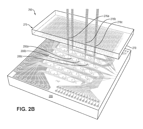
[0024] Device 290 that includes an array of MZI-coupled tunable resonators
200a,
200b, 200c, etc. is shown in FIG. 2B. An output of each diffraction grating
(not shown
in FIG. 2B, labeled 260 in FIG. 2A) can be converted to a high-NA beam using
microlens
array 275. Each diffraction grating has its own lens 276a, 276b, 276c, etc.
for NA
conversion. Points on the surface of each microlens 276a, 276b, 276c etc.
outside of the
optical axis are collimated in different directions that can be blocked. In
addition, metal
can be fabricated around the diffraction gratings (not shown) to inhibit stray
light that is
close enough to the focal point of each microlens. Metal (e.g., chrome) can be
fabricated
at the plane of the microlens array 275 to remove light that does not travel
through a
desired lens. Alternatively, where the arrays of optical modulators 200a,
200b, 200c, etc.
is formed on transparent photonic substrate 205, microlenses can be fabricated
on the
bottom surface of the substrate 205 (not shown), producing a completely
integrated
device.
[0025] Various embodiments of extracting modulated output from the optical
modulators described herein are provided below.
[0026] As shown in FIG. 1D, several PICs 160a, 160b, 160c, etc. can be
manufactured so that their edges 159a, 159b, 159c, etc. are polished to a fine
angle (e.g.,
angle <10 ), and arranged so that a combination of unidimensional arrays of
output
waveguides 155a, 155b, 155c, etc. for each PIC forms a a two-dimensional (2D)
output
array. Alternatively, as shown in FIG. 1E, a single PIC 160 can be optically
coupled to
an array of waveguides 156a, 156b, 156c, etc. to form a 2D output array 157.
[0027] As shown in FIG. 3A, in accordance with some example embodiments, in
optical modulator array 300 that comprises optical modulators 320a, 320b,
320c, etc.,
9
CA 03138309 2021-10-27
WO 2020/236574 PCT/US2020/033100
modulated output signals carried by waveguides 330a, 330b, 330c, etc. are
outputted
through diffraction gratings array 310. Diffraction gratings 310a, 310b, 310c,
etc. can be
arranged in a 2D or 1D pattern. Alternatively, as shown in FIG. 3B, optical
modulator
array 350 is shown. In array 350, each optical modulator 355a, 355b, 355c,
etc. can be
placed adjacent to diffraction grating 365a, 365b, 365c, etc, with single pump
waveguide
340 supplying optical power to each optical modulator 355a, 355b, 355c, etc.
via
waveguides 351a, 351b, 351c, etc. In some embodiments, single pump waveguide
340
can supply each row, with pickoff couplers (not shown) taking a fraction of
the optical
power for each grating-coupled modulator 355a, 355b, 355c, etc.
[0028] As an alternative to modulating laser beams at 420 nm on the UV-
visible PICs
described above, this active function can be accomplished using an already
established
PIC technology: silicon-on-insulator (SOT) PICs. SOT PIC technology, such as
the SOT
PIC 410 shown in FIG. 4, is available to modulate tens to hundreds of input
waveguides
420, and SOT carrier depletion modulations can have high speed (in excess of
20 GHz)
and can modulate relatively high power (in excess of 10 mW). See e.g., Elenion
Technologies, New York, NY. Such SOT PICs can be used to modulate the required
number of optical channels carried by input waveguides 420 in the NIR-IR
wavelength (X
= 1,100-1,700 nm). The modulated output beams 430 can be used for controlling
atomic
optical transitions above a wavelength of 1,100 nm. For controlling UV atomic
optical
transitions, the modulated output beams 430 can be subsequently frequency-
converted to,
for example, 420 nm, by coupling the SOT PIC 410 to a frequency-conversion
module
440. A PIC of AN or LN waveguides 440 can be adapted to convert an optical
signal
having a first frequency to an optical signal having a second frequency.
Within PIC 440,
two cascaded second harmonic generation (SHG) steps from 1,680 nm to 840 nm
and
then to 420 nm can be performed, or, as shown in FIG. 4, sum-frequency
generation
CA 03138309 2021-10-27
WO 2020/236574 PCT/US2020/033100
(SFG) from 1550 nm (modulated SOT PIC output 430) to 420 nm output 450 can be
performed using a yellow (e.g., dye) laser (input 445) at about 570 nm, or by
combining
approximately 1,300 nm modulated SOT PIC output 430 with a 620 nm pump (also
shown
as input 445) to produce output at 420 nm (beams 450). The waveguides 440 can
be
periodically poled or width modulated for phase matching in frequency
conversion.
[0029] In various embodiments of the systems described herein, the output
of a PIC,
positioned outside of the vacuum chamber, is imaged onto the addressable array
of
trapped particles located inside the vacuum chamber. This arrangement has
several
advantages. First, optical and electrical access to the PIC does not have to
cross the
vacuum seal of the vacuum chamber, improving the vacuum performance of the
vacuum
chamber and reducing its complexity. Second, during operation, the surface of
the PIC
can produce undesirable electric and magnetic fields that can negatively
affect the
performance of the addressable array of trapped particles. Third, during
operation, the
PIC can produce thermal fluctuations that can degrade the vacuum inside the
vacuum
chamber and the performance of the addressable array as a quantum memory.
[0030] In some embodiments, the PIC of present invention solves the problem
of a
possible relative movement of the photonic hardware and the vacuum chamber
that
contains trapped particles. This problem can be solved by allowing the same
PIC to
control beams of multiple wavelengths, such as trapping (tweezer) beams and
gate
(control) beams, that are then jointly projected onto the atom array. Such an
arrangement
beneficially allows to account for small movements of the photonic hardware
handling
the two types of beams, so that atoms are dragged along with any small motion
of the
tweezer beams while remaining within the optical field of the gate beam. (In
certain
embodiments, vibrational movements of the PIC can be additionally damped to be
less
than tens of Hz so that the atoms are not heated.) Nearby wavelengths (i.e.,
wavelengths
11
CA 03138309 2021-10-27
WO 2020/236574
PCT/US2020/033100
that are within about 20-30% of the center wavelengths) can be readily
combined onto the
same waveguide using wavelength division multiplexing devices, such as arrayed
waveguide gratings, unbalanced Mach-Zehnder interferometer add-drop
multiplexers, or
resonator-based add-drop filters. For example, for controlling Rubidium (Rb)
atoms, the
780 nm (D2 line) and 795 nm (D1 line) channels, together with trapping beams
at about
800-810 nm can all be controlled using the same layer of the photonic
integrated circuit.
As described above, the two-photon Rydberg transition employs additional laser
fields at
420 nm and 1013 nm. The 1013 nm wavelength can be combined with the
approximately
800 nm wavelengths on the same waveguide, as single-mode waveguide operation
is still
assured, although the 1013 nm laser field has a slightly larger evanescent
field than the
800 nm wavelengths. The 420 nm laser field is too short in wavelength to be
readily
controlled in the same waveguide layer.
[0031]
Referring now to FIG. 1F and FIG. 1G, and considering a 420 nm Rydberg
laser field as an example, an additional (second) layer of gate waveguides
configured to
carry a gate beam of a second wavelength, such as the 420 nm Rydberg laser
field (only
one second layer gate waveguide 170a is shown) can be added onto substrate
105,
separated from the first layer trapping waveguides that are optically coupled
to at least
one of the trapped particles of the addressable array (i.e. waveguides 155a,
b, c, etc.; only
one first layer waveguide, 155d, is shown in FIG. 1F and FIG. 1G). Second
layer gate
waveguides 170a, etc. can be disposed on PIC 160 shown in FIG. 1B. These
second
layer gate waveguides 170a, etc. can be added to the PIC during the
fabrication of
substrate 105. As shown in FIG. 1F and FIG. 1G, second layer gate waveguides
170a,
etc. can be separated from the first layer waveguides 155a, b, c, d etc., by
cladding 106,
as shown schematically and not to scale in FIG. 1F. In an example embodiment,
the
cladding can be at least 2 i_tm of silicon dioxide (5i02). Two adjacent
waveguides (such
12
CA 03138309 2021-10-27
WO 2020/236574 PCT/US2020/033100
as 155d and 170a, shown in FIG. 1F and FIG. 1G), each having a cross section
diameter
that is approximately equal to half the respective wavelength inside the
waveguide
material, as shown in FIG. 1F, can be optically coupled into one channel
through a
staggered adiabatic tapering of the two waveguides, as illustrated in FIG. 1G
with respect
to waveguides 155d and 170a. The tapered portion 171a of the thinner waveguide
170a
begins, along the length of waveguide 170a, closer to edge 159 than the
tapered portion
161d of the thicker waveguide 155d, as shown in FIG. 1G. This allows to
evanescently
transfer shorter wavelength evanescent field 172a (e.g., blue light) from a
second layer
waveguide, such as waveguide 170a, using only a single-mode section of a first
layer
waveguide, such as waveguide 155d, and both the short wavelength evanescent
field
172a and the slightly larger longer wavelength evanescent field 162d exit the
PIC at the
same point at the edge 159 of the PIC, thereby producing a combined
multiplexed
gate/trapping beam.
[0032] Accordingly, in a first example embodiment, the present invention is
a system
for optically modulating a plurality of optical channels. In a 1st aspect of
the first
example embodiment, the system comprises a power delivery module adapted to
convert
a coherent light beam into a plurality of optical channels; at least one
optical modulator,
optically coupled to the power delivery module, the at least one optical
modulator adapted
to optically modulate each of the plurality of the optical channels; and a
vacuum chamber
having a trapping plane therein, the vacuum chamber adapted to generate an
addressable
array of trapped particles at the trapping plane, wherein each of the
plurality of optical
channels is optically coupled to at least one of the trapped particles of the
addressable
array.
[0033] In a 2nd aspect of the first example embodiment, the system further
comprises
a coherent light source optically coupled to the power delivery module.
13
CA 03138309 2021-10-27
WO 2020/236574 PCT/US2020/033100
[0034] In a 3rd aspect of the first example embodiment, the power delivery
module
comprises at least one beam splitter and an optic fiber array. Other features
and example
features of the system are as described above with respect to the 1" through
the 2'
aspects of the first example embodiments.
[0035] In a 4th aspect of the first example embodiment, the power delivery
module
comprises at least one electrically controlled optical modulator adapted to
modulate the at
least one beam splitter. Other features and example features of the system are
as
described above with respect to the 1" through the 3rd aspects of the first
example
embodiments.
[0036] In a 5th aspect of the first example embodiment, the at least one
optical
modulator is configured to modulate a signal amplitude on each of the
plurality of optical
channels. Other features and example features of the system are as described
above with
respect to the 1" through the 4th aspects of the first example embodiments.
[0037] In a 6th aspect of the first example embodiment, the at least one
optical
modulator is a photonic integrated circuit (PIC). Other features and example
features of
the system are as described above with respect to the 1" through the 5th
aspects of the first
example embodiments.
[0038] In a 7th aspect of the first example embodiment, the at least one
optical
modulator comprises a plurality of electro-optically controlled Mach-Zehnder
Interferometers (MZI), each of the plurality of the MZIs adapted to modulate
one of the
optical channels. Other features and example features of the system are as
described
above with respect to the 1" through the 6th aspects of the first example
embodiments.
[0039] In an 8th aspect of the first example embodiment, each of the
plurality of MZIs
comprise waveguides comprising a material selected from lithium niobate,
lithium
tantalate, AlxGai-xN, SiN, titanium dioxide (TiO2), barium titanate (BTO), or
alumina. In
14
CA 03138309 2021-10-27
WO 2020/236574 PCT/US2020/033100
one example embodiment, the material is lithium niobate. Other features and
example
features of the system are as described above with respect to the 1" through
the 7th aspects
of the first example embodiments.
[0040] In a 9th aspect of the first example embodiment, the at least one
optical
modulator comprises a plurality of tunable resonators, each of the plurality
of tunable
resonators adapted to modulate one of the optical channels. Other features and
example
features of the system are as described above with respect to the 1" through
the 6th aspects
of the first example embodiments.
[0041] In a tenth aspect of the first example embodiment, each of the
plurality of
tunable resonators is a Mach-Zehnder Interferometer (MZI)-coupled resonator
comprising
a waveguide loop and an MZI. Other features and example features of the system
are as
described above with respect to the 1" through the 6th and the 9th aspect of
the first
example embodiments.
[0042] In an 11th aspect of the first example embodiment, each waveguide
loop
includes an electro-optically controlled section adapted to modulate the
waveguide loop's
refractive index. Other features and example features of the system are as
described
above with respect to the 1" through 6th, and the 9th through the 10th aspects
of the first
example embodiments.
[0043] In a 12th aspect of the first example embodiment, the tunable
resonator
includes a waveguide heating element adapted to modulate the waveguide loop's
refractive index. Other features and example features of the system are as
described
above with respect to the 1" through the 6th and the 9th through the 1 1th
aspects of the first
example embodiments.
[0044] In a 13th aspect of the first example embodiment, the MZI includes a
first arm
and a second arm, and the tunable resonator includes an MZI heating element
adapted to
CA 03138309 2021-10-27
WO 2020/236574 PCT/US2020/033100
modulate a refractive index of at least the first or the second arm. Other
features and
example features of the system are as described above with respect to the 1"
through 6th
and the 9th through the 12th aspects of the first example embodiments.
[0045] In a 14th aspect of the first example embodiment, the at least one
optical
modulator comprises a Silicon-on-Insulator (SOI) photonic integrated circuit
(PIC), said
SOI PIC adapted to optically modulate each of the plurality of the optical
channels. Other
features and example features of the system are as described above with
respect to the 1"
through the 6th aspects of the first example embodiments.
[0046] In a 15th aspect of the first example embodiment, the system further
comprises
a frequency-conversion module optically coupled to the SOI PIC, the frequency-
conversion module adapted to convert an optical signal having a first
frequency to an
optical signal having a second frequency. Other features and example features
of the
system are as described above with respect to the 1" through the 6th and the
14th aspects of
the first example embodiments.
[0047] In a 16th aspect of the first example embodiment, the at least one
optical
modulator is disposed on a substrate, and wherein each of the plurality of
optical channels
comprises an output waveguide. Other features and example features of the
system are as
described above with respect to the 1" through the 15th aspects of the first
example
embodiments.
[0048] In a 17th aspect of the first example embodiment, the plurality of
output
waveguides is configured to form a one-dimensional output array.
[0049] Other features and example features of the system are as described
above with
respect to the first through the 16th aspects of the first example
embodiments.
[0050] In an 18th aspect of the first example embodiment, the system
comprises a
plurality of stacked optical modulators configured to form a two-dimensional
output
16
CA 03138309 2021-10-27
WO 2020/236574 PCT/US2020/033100
array. Other features and example features of the system are as described
above with
respect to the first through the 18th aspects of the first example
embodiments.
[0051] In a 19th aspect of the first example embodiment, each of the
plurality of
output waveguides is optically coupled to an auxiliary waveguide, the
auxiliary
waveguides configured to form a two-dimensional output array. Other features
and
example features of the system are as described above with respect to the
first through the
18th aspects of the first example embodiments.
[0052] In a 20th aspect of the first example embodiment, each output
waveguide is
optically coupled to a diffraction grating. Other features and example
features of the
system are as described above with respect to the first through the 19th
aspects of the first
example embodiments.
[0053] In a 21' aspect of the first example embodiment, the diffraction
gratings are
configured to form a two-dimensional output array. Other features and example
features
of the system are as described above with respect to the first through the 21'
aspects of
the first example embodiments.
[0054] In a 22nd aspect of the first example embodiment, the system further
comprises
a microlens array, wherein each microlens of the array is optically coupled to
one of the
diffraction gratings. Other features and example features of the system are as
described
above with respect to the first through the 21' aspects of the first example
embodiments.
[0055] In a 23rd aspect of the first example embodiment, each output
waveguide is
configured to carry a trapping beam of a first wavelength, and wherein the
substrate
further includes a plurality of gate waveguides, each trapping waveguide being
optically
coupled to at least one of the trapped particles of the addressable array, and
each gate
waveguide being configured to carry a gate beam of a second wavelength,
different from
the first wavelength. Other features and example features of the system are as
described
17
CA 03138309 2021-10-27
WO 2020/236574 PCT/US2020/033100
above with respect to the first through the 22nd aspects of the first example
embodiments.
In a 24th aspect of the first example embodiment, at least one output
waveguide and at
least one gate waveguide are configured to optically couple, thereby producing
a
combined wavelength-multiplexed gate/trapping beam. Other features and example
features of the system are as described above with respect to the first
through the 23rd
aspects of the first example embodiments.
[0056] In a second example embodiment, the present invention is a method
500 for
optically modulating a plurality of optical channels. In a first aspect of the
second
example embodiment, the method comprises converting 510 a coherent light beam
into a
plurality of optical channels; delivering 520 the plurality of optical
channels to at least
one optical modulator, the at least one optical modulator adapted to optically
modulate
each of the plurality of optical channels; optically modulating 530 at least
one of the
plurality of optical channels; and optically coupling 540 at least one of the
plurality of
optical channels to at least one of a plurality of trapped particles disposed
at a trapping
plane of a vacuum chamber adapted to generate an addressable array of the
plurality of
trapped particles therein.
[0057] Having thus described several illustrative embodiments, it is to be
appreciated
that various alterations, modifications, and improvements will readily occur
to those
skilled in the art. Such alterations, modifications, and improvements are
intended to form
a part of this disclosure and are intended to be within the spirit and scope
of this
disclosure. While some examples presented herein involve specific combinations
of
functions or structural elements, it should be understood that those functions
and elements
may be combined in other ways according to the present disclosure to
accomplish the
same or different objectives. In particular, acts, elements, and features
discussed in
connection with one embodiment are not intended to be excluded from similar or
other
18
CA 03138309 2021-10-27
WO 2020/236574 PCT/US2020/033100
roles in other embodiments. Additionally, elements and components described
herein may
be further divided into additional components or joined together to form fewer
components for performing the same functions. Accordingly, the foregoing
description
and attached drawings are by way of example only, and are not intended to be
limiting.
19