Note: Descriptions are shown in the official language in which they were submitted.
CA 03138661 2021-10-29
WO 2021/021883 PCT/US2020/044000
ELECTROSURGICAL TIP
RELATED APPLICATIONS
[0001] This application claims the benefit of priority under 35 U.S.C. 119
to U.S.
Provisional Application No. 62/880,226, titled "Sputter-Coated Ceramic
Electrosurgical Tip",
filed on July 30, 2019, the entirety of which is incorporated herein by
reference.
FIELD
[0002] The present disclosure relates generally to the field of medical
devices. In
particular, the present disclosure relates to an electrosurgical surgical tip
that includes a
conductive and low-profile cutting surface to provide high current density
radiofrequency energy
with minimal thermal damage to surrounding tissues.
BACKGROUND
[0003] Many endoscopic ultrasound (EUS) guidance procedures involve
creating a
puncture tract (e.g., fistula) through the tissue layer(s) of a target anatomy
using a tissue-
penetrating needle, advancing a guidewire through the tissue-penetrating
needle to position a
distal end of the guidewire within the target anatomy and then advancing a
medical device with a
circular electrosurgical tip over the guidewire to dilate the puncture tract.
To effectively dilate
the tissue layer(s) with minimal thermal damage (e.g., charring, burning,
coagulation, etc.), the
electrosurgical tip must deliver radiofrequency energy with sufficient current
density through a
low surface area profile. Due to these design criteria, conventional
electrosurgical tips tend to be
expensive and difficult to manufacture.
[0004] It is with these considerations in mind that a variety of
advantageous medical
outcomes may be realized by the devices, systems and methods of the present
disclosure.
SUMMARY
[0005] In one aspect, the present disclosure relates to a medical device
comprising a non-
conductive base component defining a longitudinal axis and a lumen
therethrough. A conductive
material may be disposed on an outer surface of the non-conductive base
component around a
distal opening of the lumen. A conductive material may be disposed on an outer
surface of the
non-conductive base component along the longitudinal axis. The conductive
material disposed
around the distal opening may include a first layer of conductive material
bonded to the non-
conductive base component. The conductive material disposed along the
longitudinal axis may
include a second layer of conductive material bonded to the non-conductive
base component.
The first and second layers of conductive material may be sputter-coated onto
the non-
conductive base component.
1
CA 03138661 2021-10-29
WO 2021/021883 PCT/US2020/044000
[0006] In the described and other embodiments, one or more of the first and
second
layers of conductive material may be sputter-coated onto the non-conductive
base component. A
channel may be formed within the outer surface of the non-conductive base
component along the
longitudinal axis. The second layer of conductive material may extend through
the channel. The
first and second layers of conductive material may include titanium. The
conductive material
disposed around the distal opening may further include a third layer of
conductive material
bonded to the first layer of conductive material and the conductive material
disposed along the
longitudinal axis may include a fourth layer of conductive material bonded to
the second layer of
conductive material. The third and fourth layers of conductive material may be
sputter-coated
onto the respective first and second layers of conductive material. The third
and fourth layers of
conductive material may include niobium. The conductive material disposed
around the distal
opening may further include a fifth layer of conductive material bonded to the
third layer of
conductive material. The conductive material disposed along the longitudinal
axis may include a
sixth layer of conductive material bonded to the fourth layer of conductive
material. The fifth
layer of conductive material may include gold. The sixth layer of conductive
material may
include a nickel-copper alloy. The fifth and sixth layers of conductive
material may be sputter-
coated onto the respective third a fourth layers of conductive material. The
fifth layer of
conductive material may be brazed to the third layer of conductive material.
The sixth layer of
conductive material may be sputter-coated onto the fourth layer of conductive
material. A distal
portion of a conductive wire may be soldered to the sixth layer of conductive
material.
[0007] In another aspect, the present disclosure relates to a system
comprising a non-
conductive base component attached to a distal end of an electrosurgical
sheath. The non-
conductive base component may include a conductive material applied around a
distal opening
of the non-conductive base component and a strip of conductive material
applied along a
longitudinal axis of the non-conductive base component. An access cannula may
be disposable
within a lumen of the electrosurgical sheath and extendable through the non-
conductive base
component.
[0008] In the described and other embodiments, one or more of the
conductive material
and the strip of conductive material may be applied via sputter-coating. A
channel may be
formed within an outer surface of the non-conductive base component along the
longitudinal
axis. The strip of conductive material may extend through the channel. The
channel may be
disposed within a distal portion of the electrosurgical sheath. A distal
portion of a conductive
wire may be disposed within the channel. The distal portion of the conductive
wire may be
bonded to the channel using solder. The conductive wire may extend along the
electrosurgical
2
CA 03138661 2021-10-29
WO 2021/021883 PCT/US2020/044000
sheath and a proximal end of the conductive wire may be connectable to an
electrosurgical
generator. A guidewire may be extendable through a lumen of the access
cannula.
[0009] In yet another aspect, the present disclosure relates to a medical
device
comprising a non-conductive base component defining a longitudinal axis and a
lumen
therethrough. A first layer of conductive material may be disposed around an
outer surface of the
non-conductive base component in a spiral pattern. A second layer of
conductive material may
be disposed around an outer surface of the non-conductive base component in a
spiral pattern.
The first and second layers of conductive material may be electrically
insulated from each other.
[0010] In the described and other embodiments, the first and second layers
of conductive
material may be the same. The first and second layers of conductive material
may be different.
The first and second layers of conductive material may be sputter-coated to
the non-conductive
base component.
BRIEF DESCRIPTION OF THE DRAWINGS
[0011] Non-limiting embodiments of the present disclosure are described by
way of
example with reference to the accompanying figures, which are schematic and
not intended to be
drawn to scale. In the figures, each identical or nearly identical component
illustrated is typically
represented by a single numeral. For purposes of clarity, not every component
is labeled in every
figure, nor is every component of each embodiment shown where illustration is
not necessary to
allow those of ordinary skill in the art to understand the disclosure. In the
figures:
[0012] FIG. 1A provides a perspective view of an electrosurgical tip,
according to one
embodiment of the present disclosure.
[0013] FIG. 1B provides a cross-sectional view of the various layers of
conductive
material, according to one embodiment of the present disclosure.
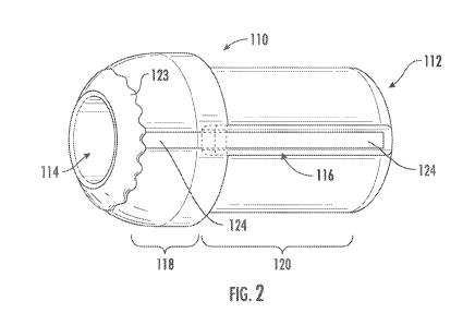
[0014] FIG. 2 provides a perspective view of an electrosurgical tip,
according to one
embodiment of the present disclosure.
[0015] FIGS. 3A-3B provide perspective views of an electrosurgical tip
housed within a
fixture for physical vapor deposition, according to one embodiment of the
present disclosure.
[0016] FIG. 4 provides a schematic illustration of a fixture (FIGS. 3A-3B)
disposed
within a physical-vapor deposition chamber, according to one embodiment of the
present
disclosure.
[0017] FIGS. 5A-5B provide perspective views of alternative electrosurgical
tip
configurations, according embodiments of the present disclosure.
[0018] FIG. 6 provides a perspective view of an electrosurgical system,
according to one
embodiment of the present disclosure.
3
CA 03138661 2021-10-29
WO 2021/021883 PCT/US2020/044000
DETAILED DESCRIPTION
[0019] The present disclosure is not limited to the particular embodiments
described
herein. The terminology used herein is for the purpose of describing
particular embodiments
only, and is not intended to be limiting beyond the scope of the appended
claims. Unless
otherwise defined, all technical terms used herein have the same meaning as
commonly
understood by one of ordinary skill in the art to which the disclosure
belongs.
[0020] Although embodiments of the present disclosure are described with
specific
reference to an electrosurgical surgical tip comprising one or more layers of
conductive metal(s)
coated onto a non-conductive ceramic base using physical vapor deposition
(PVD), electroless
plating, electrolytic plating or brazing, the disclosed devices and methods
are not limited to
medical devices or electrosurgical devices, but may include a variety of non-
conductive devices
coated with one or more layers of a variety of conductive materials.
[0021] As used herein, the singular forms "a," "an," and "the" are intended
to include the
plural forms as well, unless the context clearly indicates otherwise. It will
be further understood
that the terms "comprises" and/or "comprising," or "includes" and/or
"including" when used
herein, specify the presence of stated features, regions, steps elements
and/or components, but do
not preclude the presence or addition of one or more other features, regions,
integers, steps,
operations, elements, components and/or groups thereof.
[0022] As used herein, the term "distal" refers to the end farthest away
from the medical
professional when introducing a device into a patient, while the term
"proximal" refers to the end
closest to the medical professional when introducing a device into a patient.
[0023] In various embodiments, the present disclosure relates generally to
a medical
device (e.g., electrosurgical tip) comprising single or multiple layers of
conductive material(s)
precisely applied/deposited onto a non-conductive (e.g., ceramic) base in a
controlled location
and/or pattern and with a low surface area. The layer(s) of conductive
material(s) may provide
high current density radiofrequency (RF) energy and minimize or prevent
collateral thermal
damage to surrounding tissues. The components of the medical device local to
the layer(s) of
conductive material(s) may be electrically and thermally insulative to prevent
harm to the patient
and/or prevent thermal damage to the medical device itself.
[0024] Referring to FIG. 1A, in one embodiment, a medical device 100 (e.g.,
electrosurgical tip) of the present disclosure may include a non-conductive
base component 110
comprising a conical or tapered distal portion 118 (e.g., an increasing taper
or angled surface
extending in a constant or varying distal to proximal direction) and a
cylindrical proximal
portion 120 (e.g., with a substantially constant outer dimension). A lumen 112
may extend along
a longitudinal axis of the non-conductive base component 110. An outer
dimension of the
4
CA 03138661 2021-10-29
WO 2021/021883 PCT/US2020/044000
cylindrical proximal portion 120 may be less than a maximum outer dimension of
the tapered
distal portion 118. A groove or channel 116 may be formed within (e.g., extend
along) an outer
surface of the non-conductive base component 110 along the longitudinal axis
of the proximal
portion 120. In addition, the channel 116 may be formed within (e.g., extend
along) a proximal
end of the distal portion 118 of the non-conductive base component 110. In
various
embodiments, the non-conductive base component 110 may include a variety
insulative
materials, including, but not limited to ceramic, hard plastics and the like.
A ring 122 (e.g.,
circular ring, trace, etc.) of conductive material may be disposed on an outer
surface of the non-
conductive base component 110 around a distal opening 114 of the lumen 112. A
strip 124 (e.g.,
longitudinal strip, trace, etc.) of conductive material may be disposed on an
outer surface of the
distal and proximal portions 118, 120 along the longitudinal axis of the non-
conductive base
component 110. A distal end of the strip 124 may intersect, overlap or
otherwise contact a
portion of the ring 122 to provide a contiguous layer of conductive material
(e.g., a single/unitary
conductive layer) on/along the outer surfaces of the distal and proximal
portions 118, 120 of the
non-conductive base component 110. In various embodiments, a portion of the
strip 124 of
conductive material may be disposed within (e.g., extend through) the channel
116.
[0025] In one embodiment, the ring 122 of conductive material may include a
first layer
of conductive material bonded to the non-conductive base component 110 and the
strip 124 of
conductive material may include a second layer of conductive material bonded
to the non-
conductive base component 110. The first and second layers of conductive
material may be the
same or different materials. In various embodiments, the first and second
layers of conductive
material may include a metal (e.g., titanium) that provides the advantage of
forming/creating a
strong atomic bond (e.g., adhesion) with the non-conductive base component 110
(e.g., ceramic).
In various embodiments, the first and/or second layers of conductive material
may be applied or
deposited to the non-conductive base component 110 using physical vapor
deposition (e.g.,
sputter-coating, thermal evaporation, arc spraying, etc.), electroless
plating, electrolytic plating
or brazing, or other coating applications.
[0026] In one embodiment, the ring 122 of conductive material may include a
third layer
of conductive material bonded to the first layer of conductive material, and
the strip 124 of
conductive material may include a fourth layer of conductive material bonded
to the second layer
of conductive material. The third a fourth layers of conductive material may
be the same or
different materials (e.g., different from each other and/or different from the
first and second
layers of material). In various embodiments, the third and fourth layers of
conductive material
may include a metal (e.g., niobium) that provides the advantage of
forming/creating a strong
atomic bond (e.g., solderability) with the respective first and second layers
of conductive
CA 03138661 2021-10-29
WO 2021/021883 PCT/US2020/044000
material. In various embodiments, the third and fourth layers of conductive
material may be
applied or deposited to the non-conductive base component 110 using physical
vapor deposition
(e.g., sputter-coating, thermal evaporation, arc spraying, etc.), electroless
plating, electrolytic
plating or brazing or other coating applications.
[0027] In one embodiment, the ring 122 of conductive material may include a
fifth layer
of conductive material bonded to the third layer of conductive material, and
the strip 124 of
conductive material may include a sixth layer of conductive material bonded to
the fourth layer
of conductive material. The fifth and sixth layers of conductive material may
be the same or
different materials (e.g., different from each other and/or different from the
first, second, third
and fourth layers of material). In various embodiments, the fifth layer of
conductive material
may include a highly conductive metal (e.g., gold) that forms/creates a strong
atomic bond with
the third layer of conductive material. In various embodiments, the sixth
layer of conductive
material may include a conductive metal (e.g., nickel-copper alloy) that
form/creates a strong
atomic bond with the fourth layer of conductive material and which may form a
strong atomic
bond with a layer of solder (discussed below). In various embodiments, the
fifth and sixth layers
of conductive material may be applied or deposited to the non-conductive base
component 110
using physical vapor deposition (e.g., sputter-coating, thermal evaporation,
arc spraying, etc.),
electroless plating, electrolytic plating or brazing or other coating
applications. In one
embodiment, the layers of conductive material comprising the ring 122 (e.g.,
first, third and fifth
layers) and the layers of conductive material comprising the strip 124 (e.g.,
second, fourth and
sixth layers) may intersect (e.g., overlap, touch, contact, etc.) each other
in a variety of different
patterns, layers and/or configurations to form a contiguous layer of
conductive material (FIG.
1B). Alternatively, the fifth layer of conductive material may include a
compatible filler material
123 (e.g., gold, silver, tin, etc.) brazed or welded (FIG. 2) to the non-
conductive base component
(e.g., rather than using physical vapor deposition), and the sixth layer of
conductive material may
be applied or deposited to the non-conductive base component 110 using
physical vapor
deposition (e.g., sputter-coating, thermal evaporation, arc spraying, etc.),
electroless plating,
electrolytic plating or brazing or other coating applications. In various
embodiments, the brazed
or welded layer of conductive material may provide a cutting surface with a
geometry designed
for a specific application (e.g., a raised, enlarged or thicker cutting
surface, etc.).
[0028] In various embodiments, the ring 122 of conductive material may be
the patient
contacting portion (e.g., cutting surface) of the medical device 100 and the
strip 124 of
conductive material may be the non-patient contacting portion of the medical
device. In one
embodiment, a distal portion of a conductive wire (not shown) may be disposed
within the
groove 116 and attached to the sixth layer of conductive material by a layer
of solder formed
6
CA 03138661 2021-10-29
WO 2021/021883 PCT/US2020/044000
within the channel 116 on top of (e.g., over) the sixth layer of conductive
material and the
conductive wire disposed therebetween. A proximal end of the conductive wire
may be
electrically connected to an electrosurgical generator, as discussed below.
[0029] In various embodiments, an inner wall of the lumen 112 may not be
coated with a
conductive material to thermally and electrically insulate the lumen 112, and
any medical
devices extending therethrough (e.g., cannulas, guidewires, etc.), from the
conductive ring 122
and/or strip 124. In various embodiments, the low profile/low surface area of
the conductive ring
122 and strip 124 and the surrounding surfaces of the non-conductive base
component 110 (e.g.,
distal portion 118, proximal portion 120, lumen 112) may conduct sufficient RF
energy to
efficiently cut through/penetrate various soft tissue walls (e.g., stomach,
duodenum, gallbladder,
pancreas, liver, etc.) with minimal collateral thermal damage to the
surrounding tissues. The
ring 122 may be disposed on a distalmost portion of the distal portion 118,
such that tissue
contacts the ring 122 first, and subjected to the RF energy for penetration
through the tissue.
[0030] In various embodiments, the layer(s) of conductive material(s) may
be
applied/deposited on the non-conductive base component 110 using a line-of-
sight PVD process
that displaces metal atoms from a cathode using inert plasma atoms. Referring
to FIGS. 3A-3B,
in one embodiment, a non-conductive base component 110 of the present
disclosure may be
disposed within a fixture 130 which masks all outer surfaces of the non-
conductive base
component 110 except for the surfaces to which the ring 122 and strip 124 are
to be applied. A
plug or blank 132 may be disposed within the distal opening 114 of the non-
conductive base
component 110 to shield the lumen 112 from contact/coating with the atomized
metals.
Alternatively, the non-conductive base component 110 may be masked with a
preformed tape,
pattemable coating, photoresist or other removable coating to delineate the
ring 122 and strip
124.
[0031] Referring to FIG. 4, in one embodiment, the fixture 130 may be
positioned within
a sputter chamber 140 such that one side of the fixture 130 is directly
opposite a metal target
148a (e.g., the conductive material to be sputtered). The sputter chamber 140
may serve as an
anode, the metal target 148a may serve as a cathode and the inner surface of
the sputter chamber
140 may serve as an electrode. An inert gas 146 (e.g., argon) may be pumped
into the sputter
chamber 140, energized to a plasma state and an electric field applied to
bombard the
cathode/metal target 148a. As the plasma atoms contact the metal target 148a,
metal atoms may
be displaced from the metal target 148a and directed towards the surface of
the fixture 130. A
thin layer (e.g., approximately 50 microns) of sputtered metal 148b may then
form on the surface
of the fixture 130, including the unmasked/exposed portion of the non-
conductive base
component 110 disposed therein. In various embodiments, the fixture 130 may be
rotated within
7
CA 03138661 2021-10-29
WO 2021/021883 PCT/US2020/044000
the sputter chamber 140 to expose the other unmasked surface of the non-
conductive base
component to the metal target 148a and the process repeated. In addition, the
metal target 148a
may be replaced with a different metal target to apply/deposit the various
layers of metal to the
respective portions (e.g., ring 122 and strip 124) of the non-conductive base
component 110, as
discussed above.
[0032] Referring to FIG. 6, in one embodiment, a system 200 of the present
disclosure
may include a non-conductive base component 110 of a medical device 100
attached to a distal
end of a non-conductive electrosurgical sheath 126. In various embodiments,
the proximal
portion (not shown) of the non-conductive base component 110 may be
received/disposed within
a distal portion of the electrosurgical sheath 126 such that the channel 116
(not shown) and distal
portion of the conductive wire (not shown) disposed therein are thermally and
electrically
insulated. The conductive wire may extend along the electrosurgical sheath 126
(e.g., embedded
within a sidewall of the electrosurgical sheath) to connect a proximal end of
the conductive wire
to an electrosurgical generator. An access cannula 129 may be extendable
through the lumen (not
shown) of the non-conductive base component 110.
[0033] A variety of advantages may be realized by the devices, systems and
methods of
the present disclosure. For example, the disclosed layer(s) of conductive
material(s)
applied/deposited onto an outer surface of an electrosurgical device using PVD
may allow for
broader processing conditions at elevated temperature to provide finer surface
features (e.g.,
lower surface area, lower profile, etc.), thereby reducing production costs,
simplifying
manufacturing, minimizing collateral thermal damage and maximizing patient
safety. The
disclosed PVD process may be applied to new medical devices and/or lower the
cost of
manufacturing or modifying existing medical devices. For example, the manual
and expensive
process involved in manufacturing a conventional electrosurgical tip, e.g., in
which bi-polar
traces of gold are printed in a spiral pattern around a non-conductive tip
(Gold ProbeTM Boston
Scientific Corp., Marlborough MA.; FIG. 5A) or a steel wire is formed around a
ceramic tip (Hot
AxiosTM Boston Scientific Corp., Marlborough MA.; FIG. 5B), may be modified to
apply/deposit the bipolar or monopolar conductive layers using a PVD process.
In various
embodiments, for medical applications in which thicker conductive layers may
be required,
additional layer(s) of conductive material(s) may be applied to the PVD layer
using electroless
plating, electrolytic plating and/or brazing.
[0034] In various embodiments, the order in which the various layers of
conductive
materials outlined above (e.g., titanium, niobium, gold, nickel-copper alloy)
may be
applied/deposited to the non-conductive base component may be based on their
respective
properties of adhesion to the non-conductive base (e.g., ceramic),
solderability (e.g., the ability
8
CA 03138661 2021-10-29
WO 2021/021883 PCT/US2020/044000
to adhere/bond the highly conductive outer/top layer to the adhesive
inner/bottom layer) and/or
conductivity (e.g., of the outer/tissue contacting layer). It should be
appreciated, however, that
the present disclosure is in no way limited to these materials/metals, the
number of layers of such
materials and/or their order or pattern of deposition. A variety of conductive
materials, including,
by way of non-limiting example, titanium, niobium, gold, molybdenum, titanium
nitride,
tantalum, tungsten, platinum, palladium, iridium, tin, nickel, copper,
vanadium, silver, zinc or
other biocompatible metals, as well as alloys, oxides and nitrides of such
materials may be
applied/deposited on the disclosed medical device 100 in a variety of
orders/layers, patterns
and/or thicknesses.
[0035] In various additional embodiments, the number of layers of
conductive material(s)
applied to the non-conductive base component (e.g., the ring 122 and/or strip
124), is not limited
to the first through sixth layers outlined above, but may include a single
layer, two layers or any
number of additional layers.
[0036] In various additional embodiments, the layers of conductive material
comprising
the ring 122 (e.g., first, third and fifth layers) and the layers of
conductive material comprising
the strip 124 (e.g., second, fourth and sixth layers) may intersect (e.g.,
overlap, touch, contact,
etc.) each other in a variety of different patterns, layers and/or
configurations to form a
contiguous layer of conductive material. For example, a portion of the second
layer may partially
overlap a portion of the first layer of conductive material, a portion of the
third layer of
conductive material may partially overlap a portion of the second layer of
conductive material, a
portion of the fourth layer of conductive material may partially overlap a
portion of the third
layer of conductive material, a portion of the fifth layer of conductive
material may partially
overlap a portion of the fourth layer of conductive material and a portion of
the sixth layer of
conductive material may partially overlap a portion of the fifth layer of
conductive material.
[0037] All of the devices and/or methods disclosed and claimed herein can
be made and
executed without undue experimentation in light of the present disclosure.
While the devices and
methods of this disclosure have been described in terms of preferred
embodiments, it may be
apparent to those of skill in the art that variations can be applied to the
devices and/or methods
and in the steps or in the sequence of steps of the method described herein
without departing
from the concept, spirit and scope of the disclosure. All such similar
substitutes and
modifications apparent to those skilled in the art are deemed to be within the
spirit, scope and
concept of the disclosure as defined by the appended claims.
9