Note: Descriptions are shown in the official language in which they were submitted.
CA 03139126 2021-11-03
WO 2021/007340
PCT/US2020/041234
APPARATUS AND METHODS FOR PROVIDING ELECTRIC
ENERGY TO A SUBJECT
CROSS-REFERENCE TO RELATED APPLICATIONS
[0001] This
application claims priority to and the benefit of U.S. Patent Application
Serial
No. 16/504,623 filed July 8, 2019, entitled, "Implantable Power Adapter," the
disclosure of
which is incorporated herein by reference in its entirety.
[0002] This
application also claims priority to and the benefit of U.S. Provisional Patent
Application Serial No. 62/976,698 filed February 14, 2020, entitled,
"Apparatus and Methods
for Providing Electric Energy to a Subject," the disclosure of which is
incorporated herein by
reference in its entirety.
BACKGROUND
[0003] The
present disclosure relates generally to the field of electrical transmitters
or
stimulators used alone or in conjunction with implantable electrical devices,
and in particular,
to external electrical transmitters configured to provide transcutaneous
electrical energy to a
portion of a subject and/or to an implant disposed in the subject, and power
adapters that are
configured to be used with such an implant.
[0004]
Providing basic transcutaneous electrical nerve stimulation to a subject's
body is
known. In general, an external transmitter or stimulator (or electrical
contacts thereof) can be
placed in contact with the subject's skin and can provide stimulation directly
to a target area or
nerve or can provide electrical energy to an implanted device, which in turn,
provides
stimulation to the target area or nerve. In some known implementations,
implantable devices
receive power and/or energy from an external transmitter that can
transcutaneously apply
and/or provide a low frequency electrical current, which is received and/or
"picked-up" by one
or more electrodes or conductive portions of the implantable device. In this
manner, the energy
transfer can be similar to the transcutaneous energy transfer used in some
known devices for
delivering direct transcutaneous electrical nerve stimulation.
[0005]
Providing low frequency electrical current to a target area of the subject
and/or to
implantable devices, however, can cause pain, muscle contraction and/or
activation,
discomfort, and/or other undesirable sensations at or in non-target areas of
the subject.
1
CA 03139126 2021-11-03
WO 2021/007340
PCT/US2020/041234
Sensitivity (e.g., of a body) to a transcutaneous electrical stimulus
decreases as the frequency
of the stimulus increases, which can lower undesirable sensitivity but can
also lower efficacy
of the implantable device if the device, in turn, transmits electrical
stimulus with undesirable
characteristics (e.g., relatively high frequencies). In addition to
sensitivity, the use of an
external transmitter or stimulator to provide transcutaneous electrical
stimulus to the target area
of the subject (e.g., either directly or via an implantable device) can result
in electrical charge
build up on the skin and/or can result in undesirable heating of the external
transmitter or
stimulator associated with, for example, switching between positive and
negative phases of the
stimulation.
[0006] Thus, a
need exists for external transmitters or stimulators that can provide
transcutaneous energy to a target area of a subject and/or to implantable
devices implanted in
the subject while limiting undesirable interactions with other or non-target
portions of the body.
Furthermore, a need exists for implantable devices and/or power adapters used
with
implantable devices that receive transcutaneous energy having a desired set of
characteristics
to avoid causing pain, muscle contractions and/or activation, discomfort, and
other undesirable
sensations to portions of a subject (e.g., non-target areas or tissue).
SUMMARY
[0007] In some
embodiments, an apparatus includes a housing and a circuit at least partially
disposed in the housing. The housing can be configured to be coupled to an
implantable
electrical conductor for disposition in a body. The circuit can be configured
to be electrically
connected to a pick-up electrode of the implantable electrical conductor when
the housing is
coupled to the implantable electrical conductor. When the housing is coupled
to the
implantable electrical conductor and implanted in a body, the circuit is
configured to (1)
receive, transcutaneously from a power supply, a first energy, (2) convert the
first energy to a
second energy, and (3) transmit, to the pick-up electrode, the second energy
such that the
implantable electrical conductor can apply, via a stimulating electrode, the
second energy at
the second frequency to a region in the body.
BRIEF DESCRIPTION OF THE DRAWINGS
[0008] Unless
otherwise indicated, the drawings are not necessarily to scale. The drawings
are merely schematic representations, not necessarily intended to portray
specific parameters
2
CA 03139126 2021-11-03
WO 2021/007340
PCT/US2020/041234
of the invention. The drawings are intended to depict only typical embodiments
of disclosed
systems, apparatus, and methods.
[0009] FIG. 1A
is a schematic block diagram depicting a power adapter coupled to an
implant, in accordance with an embodiment.
[0010] FIG. 1B
is a schematic block diagram depicting an implant without a power adapter,
in accordance with an embodiment.
[0011] FIG. 2
is a schematic block diagram depicting a power adapter, in accordance with
an embodiment.
[0012] FIG. 3
is a schematic block diagram depicting an example of use of an apparatus in
conjunction with a transmitter, in accordance with an embodiment.
[0013] FIG. 4
is a flowchart depicting a method of using a power adapter, in accordance
with an embodiment.
[0014] FIGS. 5A
and 5B are schematic diagrams depicting an effect of using a power
adapter in conjunction with a transmitter, in accordance with an embodiment.
[0015] FIGS. 5C-
5E are waveforms illustrating potential waveforms used with respect to
a power adapter, in accordance with an embodiment.
[0016] FIG. 5F
is a graph illustrating the relationship between charge and frequency when
applied to an individual, according to an embodiment.
[0017] FIGS. 6A-
6F depict various views of a power adapter and/or an implant, in
accordance with an embodiment.
[0018] FIGS. 7A
and 7B depict a side view and a partial cross-sectional perspective view,
respectively, of a power adapter and an implant, in accordance with an
embodiment.
[0019] FIGS. 8A-
8C are schematic diagrams depicting circuits of a power adapter, in
accordance with various embodiments.
[0020] FIGS. 9A
and 9B are schematic diagrams depicting circuits of a power adapter, in
accordance with various embodiments.
3
CA 03139126 2021-11-03
WO 2021/007340
PCT/US2020/041234
[0021] FIGS.
10A and 10B are schematic diagrams depicting circuits of a power adapter,
in accordance with various embodiments.
[0022] FIG. 11A
depicts a non-rectified waveform (e.g., an alternating current waveform),
in accordance with an embodiment.
[0023] FIG. 11B
depicts a one-way rectified waveform, in accordance with an
embodiment.
[0024] FIG. 11C
depicts a two-way rectified waveform, in accordance with an
embodiment.
[0025] FIGS.
12A-12D are schematic diagrams depicting at least a portion of a power
adapter, in accordance with various embodiments.
[0026] FIG. 13
depicts a transmitter, and a power adapter coupled to an implant, in
accordance with an embodiment.
[0027] FIG. 14A
is a schematic diagram depicting a kit including an implantable device
and associated implements, in accordance with an embodiment.
[0028] FIG. 14B
is a schematic diagram depicting a kit including implements for coupling
a power adapter to an implant, in accordance with an embodiment.
[0029] FIGS.
15A and 15B are schematic diagrams depicting at least a portion of an
external pulse transmitter electrically connected to a load, in accordance
with an embodiment.
[0030] FIGS.
16A-16D are graphs illustrating various relationships between compliance
voltage and load voltage, in accordance with an embodiment.
[0031] FIGS.
17A-17D are schematic diagrams depicting a portion of a circuit included in
the external pulse transmitter of FIGS. 15A and 15B, and shown in a first
configuration, a
second configuration, a third configuration, and a fourth configuration,
respectively.
[0032] FIG. 17E
is a graph illustrating a current and a voltage across a load as the portion
of the circuit of FIGS. 17A-17D is transitioned between the first
configuration, the second
configuration, the third configuration, and the fourth configuration.
4
CA 03139126 2021-11-03
WO 2021/007340
PCT/US2020/041234
[0033] FIG. 18
depicts a waveform generated by an external pulse transmitter, in
accordance with an embodiment.
[0034] FIGS.
19A and 19B are graphs of an oscilloscope depicting a first waveform and a
second waveform, respectively, each of which is generated by an external pulse
transmitter, in
accordance with an embodiment.
[0035] FIG. 20
is a schematic diagram depicting at least a portion of a power adapter, in
accordance with an embodiment.
[0036] FIG. 21
is a schematic diagram depicting at least a portion of a power adapter, in
accordance with an embodiment.
DETAILED DESCRIPTION
[0037] The
embodiments and/or methods described herein are related to external electrical
transmitters or stimulators configured to provide transcutaneous electrical
energy to a target
area of a subject and/or to an implantable device implanted in the subject,
and power adapters
configured for use with at least some implantable devices. In some
embodiments, for example,
a method of using an external electrical transmitter to transcutaneously
provide electrical
energy to an implant implanted in a subject includes providing a first
electrical pulse while a
stimulating circuit is in a first configuration in which a power source (e.g.,
a voltage source
and/or a current source) is electrically connected to a load. The first
electrical pulse having a
positive voltage. The load can be, for example, a portion of the skin of the
subject positioned
between the external electrical transmitter and the implant, which can have a
capacitive element
(or property) that results in electrical charge build up across the load. The
stimulating circuit
is transitioned to a second configuration in which the power source is
electrically isolated from
the load to allow the load to discharge the electrical charge built up across
the load. The
stimulating circuit is transitioned, after a predetermined time, to a third
configuration different
from the first configuration and the second configuration, in which the power
source is
electrically connected to the load. The method includes providing a second
electrical pulse
while the stimulating circuit is in the third configuration. The second
electrical pulse having a
negative voltage (or vice versa).
[0038] In some
embodiments, an apparatus includes a housing and a circuit at least partially
disposed in the housing (e.g., as part of a power adapter). The housing can be
configured to be
CA 03139126 2021-11-03
WO 2021/007340
PCT/US2020/041234
coupled to an implantable electrical conductor for disposition in a body. The
circuit can be
configured to be electrically connected to a pick-up electrode of the
implantable electrical
conductor when the housing is coupled to the implantable electrical conductor.
When the
housing is coupled to the implantable electrical conductor and implanted in a
body, the circuit
is configured to (1) receive, transcutaneously from a power supply (e.g., an
external electrical
transmitter), a first energy, (2) convert the first energy to a second energy,
and (3) transmit, to
the pick-up electrode, the second energy such that the implantable electrical
conductor can
apply, via a stimulating electrode, the second energy at the second frequency
to a region in the
body.
[0039] In some
embodiments, an apparatus includes a power adapter having a housing and
a circuit at least partially disposed in the housing. The housing can be
configured to be coupled
to an implantable device for disposition in a body. The circuit can be
configured to be
electrically connected to the implantable device when the housing is coupled
to the implantable
electrical conductor. When the housing is coupled to the implantable
electrical conductor and
implanted in a body, the circuit can be configured to (1) receive,
transcutaneously from a power
supply (e.g., an external electrical transmitter), a first energy having a
first set of characteristics,
(2) convert the first energy to a second energy having a second set of
characteristics different
from the first set of characteristics, and (3) transfer, to the implantable
device, the second
energy such that the second energy powers the implantable device.
[0040] In some
embodiments, a method includes receiving, transcutaneously and from an
external electrical transmitter, first energy having a first set of
characteristics. The first energy
is converted, via a rectification circuit, to a second energy having a second
set of characteristics
different from the first set of characteristics. The second energy is
transferred from the
rectification circuit to a stimulating electrode of an implantable electrical
conductor such that
the implantable electrical conductor applies, via the stimulating electrode,
the second energy
to a target nerve internal to a body.
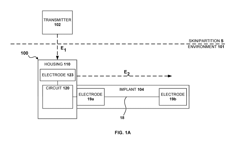
[0041] FIG. 1A
is a schematic block diagram depicting a power adapter 100 coupled to an
implant 104, in accordance with an embodiment. As shown in FIG. 1A, the power
adapter 100
includes a housing 110, a circuit 120 at least partially disposed in the
housing 110 and an
electrode 123. The power adapter 100 can be configured to be coupled or
interconnected to
implant 104 such as at and via the housing 110, as shown in FIG. 1A. The power
adapter 100
can be configured to operate, in conjunction with and when coupled to the
implant 104, in an
6
CA 03139126 2021-11-03
WO 2021/007340
PCT/US2020/041234
environment of and internal to a body, such as environment 101, which can be
defined, for
example, by a boundary such as skin/partition S, such as shown in FIG. 1A.
[0042] FIG. 1B
is a schematic block diagram depicting the implant 104 without a power
adapter being couple thereto (e.g., the power adapter 100 shown in FIG. 1A).
As shown in
FIG. 1B, the implant 104 includes electrodes 19a and 19b. The power adapter
100, when
coupled to the implant 104 (e.g., at and/or over electrode 19a such as shown
in FIG. 1A), can
be configured to operate in the environment 101, in conjunction with the
implant 104 and a
device such as an external electrical transmitter 102 to, for example, enable
(e.g., supply power
to) the implant 104 to perform or otherwise carry out a medical procedure,
task, operation, or
measurement in the body. More specifically, the electrode 123 can be
configured to receive
electrical energy from external electrical transmitter 102, the circuit 120
can convert the
frequency and/or waveform of the electrical energy, and the power adapter 100
can provide the
converted electrical energy to the electrode 19a, as described in further
detail herein.
[0043] For
example, the power adapter 100 can be configured to receive, from the external
electrical transmitter 102 and via the electrode 123, energy Ei (referred to
herein as "first
energy") such as a first form or quantity of energy, power, or signals
(collectively, "energy")
having a first characteristic or set of characteristics (e.g., a first
frequency, a first waveform, a
first burst pattern, and/or the like). The first energy El, due to the first
characteristic(s), may
be unsuitable for use in powering and/or otherwise provided to or used by the
implant 104.
Accordingly, to provide energy suitable for use by the implant 104 such that
the implant 104
is enabled to perform the medical procedure in the body, the power adapter 100
can be
configured to transform, rectify, derive, adapt, and/or otherwise convert the
first energy Ei to
a second energy E2, including a second form or quantity of energy, power, or
signals
("collectively, energy") having a second characteristic or set of
characteristics (e.g., a second
frequency, a second waveform, a second burst pattern, and/or the like). As
shown in FIG. 1A,
the power adapter 100 can be configured to convert the first energy Ei to the
second energy E2
such that the second energy E2, due to the second characteristic(s), is
suitable for use by the
implant 104, such that the implant 104 is enabled to perform, using the second
energy E2, the
medical procedure in the body (e.g., including providing, via the second
energy E2, stimulation,
activation, or excitation of tissue, nerves, or muscles in the body, or
blocking of excitation or
activation of the tissue, nerves, or muscles). The power adapter 100 can be
configured to
transfer or input the second energy E2 to the implant 104 to enable (e.g.,
powering of, or control
7
CA 03139126 2021-11-03
WO 2021/007340
PCT/US2020/041234
over) the implant 104 in performing or otherwise carrying out the medical
procedure in the
body. More particularly, when the power adapter 100 is coupled to the implant
104, the circuit
120 is electrically coupled to the electrode 19a (e.g., via a conductor or the
like not shown in
FIG. 1A) such that the second energy E2 that is generated by the circuit 120
is provided as an
input to the electrode 19a.
[0044] The
housing 110 can be configured to be coupled to the implant 104 for disposition
in a body therewith. The electrode 123 of the power adapter 100 can be
configured to receive,
transcutaneously with respect to the body, the first energy Ei (e.g., high
frequency electrical
bursts, low frequency pulses, etc.) for conversion and transfer to implant 104
for application
(e.g., in the form of bursts or pulses, to be used by the implant 104, etc.),
as described herein.
Skin/partition S can include, for example, a barrier, partition, skin, and the
like, such as of the
body of a subject, including, for example, a person, patient, and the like.
The body of the
subject can include an (e.g., internal) environment, such as environment 101.
[0045] The
external electrical transmitter 102 can be or include, for example, an
external
pulse transmitter (EPT), a power source or supply, an energy source or supply,
a voltage source
or supply, a (wireless) energy transfer device, a signal transmitter, and/or
the like. The external
electrical transmitter 102 can be any suitable configuration. Various terms
are used herein to
refer to an external transmitter and should be understood to be
interchangeable unless the
context clearly dictates otherwise. For example, such terms can include
"external electrical
transmitter," "external electrical stimulator," "external pulse transmitter,"
"external pulse
generator," "electrical pulse generator," "electrical transmitter,"
"electrical stimulator," "power
supply," "transcutaneous electrical nerve stimulator (TENS)," and/or the like.
For simplicity,
the term "transmitter" is generally used herein to refer to such devices.
[0046] The
transmitter 102 can be configured to transmit energy (e.g., the first energy
Ei)
into a body of a subject, which can be received, for example, by the power
adapter 100 and
used in and/or by implant 104 (e.g., when power adapter 100 is coupled to
implant 104). For
example, the transmitter 102 can be configured to transmit the energy into the
body for receipt,
or pick-up (e.g., of some portion of the energy), by the power adapter 100.
Subsequently, the
energy, after being received by the power adapter 100, can be transferred from
the power
adapter 100 to the implant 104 (e.g., the second energy E2, shown in FIG. 1A).
In some
instances, the energy can be converted to a form (e.g., from a first form of
energy to a second
form of energy) suitable for use in powering the implant 104, such as to
enable the implant 104
8
CA 03139126 2021-11-03
WO 2021/007340
PCT/US2020/041234
to perform a medical procedure in the body, as described herein. In other
instances, the power
adapter 100 can have and/or can be placed in a pass-through configuration
and/or state in which
the energy received from the transmitter is transferred to the implant without
substantially
modifying the characteristics of the energy. Accordingly, the second energy E2
transferred
from the power adapter 100 to the implant 104 can have characteristics similar
to or different
from characteristics of the first energy Ei received from the transmitter 102.
[0047] The
transmitter 102 can be configured to transmit the energy into a body of a
subject
transcutaneously, at various levels of current, or electrical charge, and at
current and/or
frequency levels, to avoid causing adverse sensory or motor activation or
stimulation (e.g.,
responses at or in undesirable locations of the body near the electrodes of
the transmitter 102,
referred to herein as a "local response") in and by the body. In some
instances, the transmitter
102 can deliver energy transcutaneously via hydrogel, wetted cloth, and/or
other electrodes
attached to the skin. In some instances, the transmitter 102 can be configured
to transmit the
energy via output of a time-varying voltage (or electrical potential), current
(or electrical
charge), or electromagnetic field ¨ at a predetermined frequency or range of
frequencies, and
with a predetermined waveform. In some implementations, the output from the
transmitter 102
can include, for example, a time-varying flow of electrical charge. The time-
varying flow of
electrical charge can include, for example, electrical bursts, electrical
pulses, and/or the like
("electrical burst(s)" or "burst(s)"), such as in the form of a train or
series of high frequency
bursts, including, for example, electrical, electromagnetic, and/or magnetic
bursts. In some
implementations, the output of the transmitter 102 can include a train or
series of low frequency
bursts, where each burst includes a single low frequency pulse. In some
implementations, the
output of the transmitter 102 can include a train or series of bursts
including any suitable
combination of one or more low frequency energy bursts and one or more high
frequency
energy bursts. In some instances, the one or more low frequency energy bursts
can have one
or more characteristics configured to result in a desirable local response in
and by the body
such as, for example, increased blood flow within a region of the body
adjacent to or relatively
near the transmitter 102, while the one or more high frequency energy bursts
can be received
by, for example, the power adapter 100.
[0048] In some
implementations, the predetermined frequency or range of frequencies can
include, for example, a frequency or range of frequencies between
approximately 10 kilohertz
(kHz) and 100 kHz. The predetermined frequency or range of frequencies can
otherwise
9
CA 03139126 2021-11-03
WO 2021/007340
PCT/US2020/041234
include a frequency or range of frequencies at which the energy output from
the transmitter
102 can be applied, such as to a body of a subject, without causing an
undesirable response, or
stimulation ("response"), such as an undesirable local motor response, in and
by the body near
the electrodes of the transmitter. For example, FIG. 5F is a graph
illustrating a relative
stimulation intensity as a function of stimulation frequency. In some
implementations, the
transmitter 102 can be configured to provide energy or stimulation at a
frequency within the
shaded area identified as the "Operational Window." Moreover, as the frequency
increases,
the stimulation intensity prior to causing an undesirable local response also
increases, as
described in further detail herein.
[0049] In some
implementations, the transmitter 102 can be configured to transmit the
energy (e.g., first energy El) at a frequency and charge configured to avoid
causing a sensation
or response in or by the body tissues (e.g., a local response). In some
implementations, the
transmitter 102 can be configured to transmit energy (e.g., the first energy
El) at a frequency
and charge configured to cause a desirable local response (e.g., increased
blood flow or other
desired local responses). In some implementations, the transmitter 102 can be
configured to
transmit energy (e.g., the first energy El), in which a first portion of the
energy is at a first
frequency and/or charge configured to avoid causing a local response and a
second portion of
the energy is at a second frequency and/or charge configured to cause the
desirable local
response. In some implementations, the transmitter 102 can be configured to
transmit the first
portion of the energy and the second portion of the energy in any suitable
combination, pattern,
interval, sequence, and/or the like.
[0050] In some
implementations, the predetermined waveform can include, for example, a
sinusoidal waveform, a rectangular waveform, a triangular waveform, or any
other suitable
waveform (as described in further detail herein with reference to FIGS. 5C-
5E). The
predetermined waveform can otherwise include any suitable type of waveform.
Operating
parameters by which the transmitter 102 can be configured to transmit the
energy can include,
for example, pulse width, pulse frequency, current magnitude, current density,
power
magnitude, power density, and the like.
[0051] The
transmitter 102 can be configured to transmit the energy by application of the
output to a body of a subject at or with respect to a position, region, or
location surrounding,
encompassing, or adjacent to a position or location at which the power adapter
100 or the
implant 104 are disposed (e.g., implanted) in the body, such as shown in FIG.
1A. For example,
CA 03139126 2021-11-03
WO 2021/007340
PCT/US2020/041234
the transmitter 102 can be configured to transmit the energy by application of
the output to the
body, transcutaneously, such as along or with respect to a path (e.g.,
electrical path, conductive
path) at least partially disposed internal to the body, and interconnecting
the transmitter 102,
the power adapter 100, and the implant 104. That is, the path can be defined,
in part, by the
body into which the transmitter 102 is configured to transmit the energy, such
as by the portion
of the body between the transmitter 102, power adapter 100, and implant 104.
[0052] The
implant 104 represents an implant such as an implantable device, including,
for
example, an implantable electrical conductor, and/or the like ("implant" or
"implantable
device" or "implantable electrical conductor"). The implant 104 can be
configured to be
powered by and/or otherwise use energy received from an external device such
as an external
transmitter or power supply (e.g., transmitter 102), via a power adapter
(e.g., power adapter
100), to perform a medical procedure in a body (e.g., in environment 101) of a
subject, as
described herein. In some implementations, the implant 104 can include an
onboard energy
source, energy storage device, and/or the like, such as a battery. Such a
battery can, for
example, store and/or be recharged by the energy received transcutaneously.
[0053] For
example, in some instances, the implant 104 can be or include an implantable
electrical conductor, such as of an implantable stimulation device, or
stimulator, configured to
operate in the body, and to be powered, via the power adapter 100, by an
external device such
as the transmitter 102. In these instances, the implantable stimulation
device, or stimulator,
can be or include, for example, a nerve stimulator, an artificial pacemaker,
and/or the like. In
other instances, the implant 104 can be or include an implantable electrical
conductor, such as
of a fluid conveyance device, or fluid conveyor, such as a pump or compressor
(e.g., insulin
pump), or a vacuum, suction, or depressurizing device. In other instances, the
implant 104 can
be or include an implantable electrical conductor, such as a sensor,
transducer, monitor, and/or
recorder, including, for example, an electrocardiography (ECG) sensor, a heart
rate monitor, a
Holter monitor, and/or the like. The implant can otherwise be or include any
suitable type and
number of implantable electrical conductors.
[0054] As shown
in FIG. 1B, the implant 104 includes electrodes 19a and 19b,
interconnected over conductor 18. The implant 104 can include an input and an
output, such
as at the electrode 19a and the electrode 19b, respectively. For example, the
implant 104 can
be configured to receive energy at the input (e.g., at the electrode 19a), and
to provide energy
at the output, (e.g., at the electrode 19b). Energy can be conveyed between
the input (e.g.,
11
CA 03139126 2021-11-03
WO 2021/007340
PCT/US2020/041234
electrode 19a) and the output (e.g., electrode 19b) via an implantable
electrical conductor (e.g.,
conductor 18) of the implant 104. The implant 104 can be configured to
receive,
transcutaneously and at the electrode 19a, energy from a transmitter such as
transmitter 102.
The energy can be received, for example, to power the implant 104, to control
the implant 104
(e.g., as in performing a medical procedure), and/or the like.
[0055] In some
implementations, the implant 104 can be configured to receive energy from
the transmitter 102 via the power adapter 100. For example, in some instances,
such as when
the power adapter 100 is connected to the implant 104, as shown in FIG. 1A,
the power adapter
100 can be configured to receive the first energy Ei (e.g., having a first
frequency, waveform
and/or other characteristic) from the transmitter, for conversion of the first
energy to the second
energy E2 (e.g., having a second frequency, waveform and/or other
characteristic), and transfer
of the second energy E2, from the power adapter 100 and to the implant 104,
such as by input
to the implant 104 at the electrode 19a, such that the implant 104 receives
the second energy
E2 (e.g., for output at electrode 19b). In some implementations, when the
power adapter 100
is not connected to the implant 104 (e.g., as shown in FIG. 1B), the electrode
19a can receive
the second energy E2 directly. By connecting the power adapter 100 to the
implant 104 and
over the electrode 19a, the implant 104 can be retrofitted and/or adapted to
receive the first
energy El rather than the second energy E2. That is, when the power adapter
100 is connected
to the implant 104, such as shown in FIG. 1A, the power adapter 100 can
prevent the electrode
19a from directly receiving energy. The energy output by electrode 19b can be
detected and/or
received by the transmitter 102 (e.g., by a skin electrode (not shown in FIGS.
1A or 1B) to
complete an electrical circuit including the transmitter 102, the housing 110
and the implant
104.
[0056] The
electrodes 19a and 19b can each include one or more electrodes, electrical
contacts, electrical terminals, and the like. The electrode 19a can include an
input electrode
and the electrode 19b can include an output electrode. For example, the
electrode 19a can
include an input electrode such as a receiving electrode, a pick-up electrode,
and/or the like
(referred to herein as "pick-up electrode"). In some implementations, such as
those in which
the implant 104 is a stimulation device, the electrode 19b can include an
output electrode such
as a stimulating or stimulation electrode, a stimulation lead, and/or the like
(referred to herein
as "stimulating electrode" or "stimulation electrode"). In some
implementations, the electrode
19a can include and/or can be formed of a material such as a titanium (Ti),
titanium-nitride
12
CA 03139126 2021-11-03
WO 2021/007340
PCT/US2020/041234
(TiN), platinum-iridium (Pt-Ir) compound, and/or the like. In some
implementations, the
electrode 19b can include and/or can be formed of a material such as a
platinum (Pt), iridium
(Ir), a platinum-iridium (Pt-Ir) compound, or alloy, and/or the like. The
conductor 18 can
include any suitable electrical conductor, electrical lead, and/or conductive
material over which
the electrodes 19a and 19b can be interconnected. For example, the conductor
18 can include
a path such as a conductive path or an electrical path configured to
interconnect the electrodes
19a and 19b over the implant 104. The conductor 18 can include and/or can be
formed of a
material such as an inert or non-reactive material, or any other material
suitable for use in a
body of a subject, in accordance with embodiments described herein.
[0057] The
housing 110 can be or can include any suitable type of housing or casing. For
example, the housing 110 can include a housing such as an hermetically sealed
casing, or can,
configured to house or otherwise contain one or more circuits (e.g., circuit
120), and, having a
feedthrough, inner contact (e.g., electric conductor), one or more mating
features (e.g., grip
mechanism assembly) configured to electrically and mechanically couple to and
make contact
with a pick-up electrode (e.g., electrode 19a of implant 104), and a sleeve
(e.g., for mechanical
and/or electrical protection). The housing 110 can be configured to at least
partially house one
or more circuits, including, for example, the circuit 120. The housing 110 can
be configured
to be coupled to an implant such as implant 104 for disposition, with implant
104 (and the
circuit 120), in a body of a subject. The housing 110 can be configured to
mechanically insulate
the circuit 120 from the body, including, for example, from an environment in
the body such
as environment 101. For example, the housing 110 can be configured to insulate
the circuit
120 from, for example, an environment such as environment 101 in the body of
the subject,
such as when the housing 110 is coupled to implant 104 and disposed in
environment 101, such
as by implantation with implant 104 in the body. The housing 110 can include
any suitable
housing capable of attaching, coupling, connecting, interconnecting, or
otherwise being added,
mechanically, electrically, and otherwise, to an implant such as implant 104,
as described
herein. The housing 110 can include any suitable type and number of
components, such as
including resistors, capacitors, transistors, diodes, inductors, an energy
source, energy storage
device, and/or the like. In some implementations, the housing 110 does not
include an energy
source, energy storage device, and/or the like, which can be or include, for
example, a battery
or other chemical source of energy. In other implementations, the housing can
include an
energy storage device (e.g., battery, energy storage capacitor, etc.) that can
be used to power
the implant 104 and/or can be recharged by receiving the transcutaneous
transfer of energy, as
13
CA 03139126 2021-11-03
WO 2021/007340
PCT/US2020/041234
described herein. In some implementations, the housing 110 can be or include,
for example, a
hermetically sealed can configured to at least partially house the circuit
120.
[0058] The
circuit 120 can be or include a circuit such as an integrated circuit (IC),
and/or
the like. The circuit 120 can be configured to be electrically connected to an
implantable device
such as the implant 104 when the housing 110 is coupled to the implant 104,
such as at the
electrode 19a. For example, the circuit 120 can be configured to electrically
connect to the
implant 104, when the housing 110 is coupled to the implant 104, such as at a
pick-up electrode
(e.g., electrode 19a) of the implant 104, to enable the circuit 120 to provide
energy (e.g.,
transformed power, conditioned signals) to the implant 104. The energy can be
provided, by
the circuit 120 and to the implant 104, via input to the implant 104 at the
pick-up electrode
(e.g., via a conductor or electric interface in electric communication with
the electrode 19a).
The circuit 120 can be configured to receive the energy (e.g., for conversion
of the energy and
transfer of the converted energy to implant 104) from a transmitter such as
transmitter 102, as
described herein. The circuit 120 can include various components, such as
described herein
with reference to FIG. 2.
[0059] As an
example, in use, the power adapter 100 can be configured to be implanted, in
a coupled or interconnected state with implant 104, in a body of a subject.
For example, the
power adapter 100 can be configured to be coupled to implant 104 by attachment
of the housing
110 over a pick-up electrode (electrode 19a) of the implant 104. In some
instances, the power
adapter 100 can be configured to be retrofit to an existing implant in a body
of a subject, such
as the implant 104. For example, the power adapter 100 can be configured to be
mated to the
existing implant such as by crimping, or the like. Once the power adapter 100
is implanted in
the body with the implant 104, operating parameters, including, for example,
stimulation
parameters, and the like, can be set (e.g., at transmitter 102), as described
herein. Accordingly,
the power adapter 100¨ along with the transmitter 102 and the implant 104¨ can
be configured
for use, such as by the subject of the body (in which the power adapter 100 is
implanted with
the implant 104).
[0060] In other
implementations, the power adapter 100 can be integral to the implant 104.
For example, in some implementations, the power adapter 100 can be provided as
part of or
embedded in the implant 104, such as in a pre-coupled or ¨interconnected state
with the implant
(e.g., via interconnection to electrode 19a). Similarly stated, in such
implementations, the
functions of the power adapter 100 (as described herein) can be part of and/or
integrated into
14
CA 03139126 2021-11-03
WO 2021/007340
PCT/US2020/041234
the implant. In such implementations, a separate power adapter 100 is not
needed and/or used
to receive the transcutaneous energy transfer.
[0061] In some
implementations, such as those in which the implant 104 is a stimulation
device and the electrode 19b includes an output electrode such as a
stimulating electrode, the
power adapter 100 can be configured to convert the first energy Ei (e.g., from
transmitter 102)
to the second energy E2, for input of the second energy E2 to the implant 104
to enable the
implant 104 in performing a medical procedure. In such implementations, the
medical
procedure can include, for example, a medical procedure in which the implant
104 is
configured to provide stimulation, activation, excitation, and the like
("stimulation") of tissue,
nerves, or muscles in a body of a subject. In such implementations, the
implant 104 can be
configured to perform the medical procedure in the body via output of the
second energy E2 at
the electrode 19b. In such implementations, the second energy E2 can include,
for example, a
sequence of low frequency pulses or bursts and/or a sequence of high frequency
pulses or
bursts. Specifically, the second energy E2 can include, for example,
interlaced delivery of low
and high frequency energy, stimulation, bursts, and/or pulses. The medical
procedure can be
performed, for example, to activate a cutaneous receptor, a muscle, and/or a
nerve of the body.
[0062] FIG. 2
is a schematic block diagram depicting a power adapter 200, in accordance
with an embodiment. As shown, the power adapter 200 includes a housing 210 and
a circuit
220 at least partially disposed in the housing 210. The power adapter 200 can
be configured
to be coupled or interconnected to an implant (e.g., the implant 104) for
disposition in a body,
such as to operate in an environment (e.g., the environment 101) of and
internal to the body.
The circuit 220, when the housing 210 is coupled to an implant (e.g., the
implant 104) and
implanted in a body, can be configured to electrically interconnect (e.g., via
an electrode 223b)
to a stimulating electrode of the implant. The power adapter 200 can be
structurally and/or
functionally similar to other power adapters (e.g., the power adapter 100)
shown and described
herein.
[0063] The
circuit 220 includes a rectification circuit 221 and an electrode 223a (e.g.,
pick-
up electrode). The rectification circuit 221 can be or include, for example, a
halfwave-
rectification circuit or a fullwave-rectification circuit. For example, in
some instances, the
rectification circuit 221 can include a resistor 222, a diode 224, and a
capacitor 226. While not
shown or described with respect to FIG. 2, in other implementations (e.g., as
shown and
described with respect to 9A, 9B and/or 10), the circuit can include another
capacitor and/or an
CA 03139126 2021-11-03
WO 2021/007340
PCT/US2020/041234
inductor to provide protection at frequencies used with respect to Magnetic
Resonance (MR)
devices such as, for example, Magnetic Resonance Imaging (MRI) devices. The
rectification
circuit 221 can be configured to selectively convert received energy (e.g.,
received from the
transmitter 102 via the electrode 223a). For example, the rectification
circuit 221 can be
configured to convert first energy by rectification of the first energy to
provide second energy
(e.g., via the electrode 223b). In some instances, the second energy can be
substantially
positive DC or substantially negative DC. As an example, the rectification
circuit 221 can be
configured to convert and filter received signals in a manner similar to that
of an amplitude
modulation (AM) receiver.
[0064] The
capacitor 226 can be or include, for example, a direct current (DC) blocking
capacitor. The capacitor 226 can be configured to maintain a level of charge
balance of the
rectification circuit 221. For example, the capacitor 226 can be configured to
provide charge
balancing of energy transmitted from the rectification circuit 221. In some
implementations,
such as those in which the implant 104 is a stimulation device, a type or
characteristic of the
capacitor 226 can be chosen, for example, based on a characteristic (e.g.,
operating condition)
such as tissue-electrode capacitance, such as of a pick-up electrode (e.g.,
electrode 19a) and a
stimulating electrode (e.g., electrode 19b) of the implant 104, with respect
to tissue internal to
a body of a subject (e.g., in environment 101). In such implementations, the
capacitor 226 can
effectively be connected in series with the pick-up electrode and the
stimulating electrode. In
a serial connection of capacitors, the capacitor with the least amount of
capacitance (i.e., the
capacitor with the smallest measure of capacitance) determines the combined
capacitance of
the capacitors (e.g., which is substantially equal to the capacitance of the
capacitor with the
least relative amount of capacitance). Accordingly, the capacitor 226 can be
chosen or
configured to have a particular value or measure of capacitance to not
decrease the overall
capacitance of the path (e.g., interconnecting the capacitor 226, the pick-up
electrode, and the
stimulating electrode) based on the effective capacitance of the tissue-
electrode capacitance of
the pick-up electrode and the stimulating electrode.
[0065] As an
example, where the tissue-electrode capacitance is approximately 4
microfarad ( F), the capacitor 226 can be chosen or configured to have a value
or measure of
capacitance of approximately 4 [tF, or greater. In this example, the value of
the capacitor 226
can be chosen or configured based on the tissue-electrode capacitance of the
tissue internal to
the body and the pick-up electrode (e.g., electrode 19a) and the stimulating
electrode (e.g.,
16
CA 03139126 2021-11-03
WO 2021/007340
PCT/US2020/041234
electrode 19b) of the implant 104. In some implementations, the capacitor 226
can be chosen
or configured to have a value or measure of capacitance that does not decrease
but supports
and/or maintains an overall capacitance of the conductive path (e.g., the path
interconnecting
a pick-up electrode with a stimulating electrode) of the implant 104.
[0066] The
diode 224 can be or include, for example, a rectifying diode. In some
implementations, the diode 224 can be or include a rectifying diode such as a
Schottky diode,
a silicone diode, and/or the like. In some implementations, a type or
characteristic of the diode
224 can be chosen, for example, based on a characteristic such as a magnitude
of a voltage
drop (e.g., in a forward direction) over the diode 224. For example, the type
of the diode 224
can be chosen to reduce a magnitude of the voltage drop over the diode 224. In
this example,
the type of the diode 224 can be chosen to be or include a Schottky diode
(e.g., instead of a
silicon diode) to reduce the magnitude of the voltage drop over the diode 224
(e.g., compared
to that of the silicon diode), and to thereby achieve a higher pick-up ratio
(e.g., compared to
that of a silicone diode). In some implementations, a type of the diode 224
can be chosen based
on or to facilitate any suitable characteristic, such as amount of leak
current, amount of back
leak current, a discharge rate (e.g., of capacitor 226) between applied
electrical bursts, and/or
the like. For purposes of the present disclosure "pick-up" ratio refers to the
amount of energy
received by the implant relative to the amount of energy sent by the external
transmitter. For
example, a pick-up ratio of 0.5 indicates that the amount of energy received
by the implant is
approximately half the amount of energy sent by the external pulse
transmitter.
[0067] The
resistor 222 provides a discharge path (from rectification circuit 221) for
the
capacitor 226. In some implementations, a type or characteristic of the
resistor 222 can be
chosen, for example, based on a characteristic of the rectification circuit
221 including, for
example, a discharge path characteristic of the rectification circuit 221. For
example, the
resistor 222 can be chosen to have a measure or value of resistance greater
than an effective
resistance of the diode 224, to prevent bypass (e.g., by electrical current)
of the diode 224 in
use (e.g., of the power adapter 200 with an implant such as implant 104). In
some
implementations, a type or characteristic of the resistor 222 can be chosen,
for example, based
on an applied frequency or frequency range of the energy (e.g., electrical
signals, electrical
bursts) from transmitter 102, a burst repetition frequency of the applied
frequency or frequency
range of the energy, a burst duration of the applied frequency or frequency
range of the energy,
and/or the like.
17
CA 03139126 2021-11-03
WO 2021/007340
PCT/US2020/041234
[0068] FIG. 3
is a schematic block diagram depicting an example use of a power adapter
300 in conjunction with a transmitter 302, in accordance with an embodiment.
As shown, the
power adapter 300 includes a housing 310 (labeled "add-on receiver") and a
circuit (not shown)
at least partially disposed in the housing 310. The power adapter 300 can be
structurally and/or
functionally similar to other power adapters (e.g., 100, 200) described
herein.
[0069] The
transmitter 302 can be configured to send or otherwise provide energy to power
adapter 300 (for powering and/or supplying energy to implant 304) via path
303. In some
implementations, the electrical pulse generator (e.g., transmitter 102,
transmitter 302) can
include, for example, a power supply. The path 303, along which the energy is
received,
transferred, and applied, can include, for example, a portion of the body of
the subject between
the transmitter 302 (e.g., at a gel and/or cloth electrode of the transmitter
(not shown)) and the
power adapter 300 (when disposed with implant 104 in the body).
[0070] For
example, the power adapter 300, the housing 310, and the circuit can be
structurally and/or functionally similar to the power adapter 100, the housing
110, and the
circuit 120, respectively, as described herein. The power adapter 300 can be
configured to be
coupled, via the housing 310, to an implant such as implant 304 for
disposition in a body with
implant 304, such as beneath skin and in environment 301 of the body. The
power adapter 300
can be configured to be attached or coupled to implant 304 such that the pick-
up electrode of
implant 304 is electrically insulated from the environment 301 (e.g., when
implant 304 and
power adapter 300 are implanted in a body). The power adapter 300 can be
configured to
receive energy from the transmitter 302 for conversion and transfer to implant
304, and
application, via a stimulating electrode of implant 304, to a target site or
object in the body.
[0071] The
transmitter 302 can be structurally and/or functionally similar to the
transmitter
102, as described herein. For example, the transmitter 302 can include an
external transmitter
(labeled "transmitter") and a patch (not shown) including one or more gel
electrodes (labeled
"gel electrode"). In some implementations, the external transmitter can
include, for example,
a high frequency transmitter. While shown in FIG. 3 as gel electrodes, in some
implementations, the patch can include, for example, a gel patch, a hydrogel
patch, a cloth
patch, and/or the like, including, for example, electrodes such as gel
electrodes, hydrogel
electrodes, cloth electrodes, and/or the like. In some implementations, the
patch can include a
disposable patch. The transmitter 302 can be configured to transmit energy
transcutaneously
18
CA 03139126 2021-11-03
WO 2021/007340
PCT/US2020/041234
into the body of a subject (e.g., for receipt by the circuit disposed in the
housing 310), such as
by application, via the patch, of the output of the transmitter 302 to the
body.
[0072] Implant
304 can be structurally and/or functionally similar to implant 104, as
described herein. For example, implant 304 can include an electrical conductor
or lead (labeled
"lead"), a stimulating electrode (labeled "stimulating electrode"), and a pick-
up electrode (not
shown), over which the power adapter 300 can be attached or coupled, such as
described herein
with reference to FIG. 1, and shown in FIG. 3. The lead of implant 304 can
include, for
example, a conductive path interconnecting the stimulating electrode and the
pick-up electrode.
The lead of implant 304 can be or include, for example, an electrical
conductor such as a coiled
wire (Pt-Ir) conductor disposed within a silicone sheath, or tubing. For
example, the lead of
implant 304 can be insulated (e.g., from tissue in the environment 301) by the
silicone tubing
and by silicone backfill disposed in and configured to close the tubing at
each end. Implant
304 can be configured to receive, transcutaneously and via the power adapter
300 (e.g.,
disposed at the pick-up electrode of implant 304), energy (e.g., electrical
signal,
electromagnetic signal, magnetic signal) from the transmitter of the
transmitter 302. For
example, implant 304 can be configured to receive the energy to apply, via the
stimulating
electrode, a stimulus (e.g., electrical bursts, electrical pulses) to a target
site or object in a body
of a subject. In some implementations, implant 304 can include, for example,
three or more
stimulating electrodes (e.g., such as the electrode 19b).
[0073] In use,
the power adapter 300 can be configured to receive, transcutaneously from
the transmitter 302, transdermal high frequency bursts of energy (e.g.,
electrical energy). The
energy can be received at, or can otherwise include, for example, a first
frequency of between
about 10 kHz and 100 kHz, or greater. In other instances, the first frequency
can be between
100 kHz and 3 megahertz (MHz). In yet other instances, the first frequency can
be 10 MHz or
less and/or any other suitable frequency. The received energy can be
converted, by the power
adapter 300, to a form suitable for use in providing stimulation, activation,
or excitation (e.g.,
of tissue, nerve, muscle) in a body of a subject. For example, the received
energy can be
converted, by the power adapter 300, to a second energy (e.g., stimulation
current) having a
second frequency less than the first frequency, such as, for example about 1
kHz. In other
implementations, the second frequency can be between 1 kHz and 10 kHz. In yet
other
implementations, the second frequency can be between 500 Hz and 30 kHz. The
energy
conversion can include, for example, rectification and charge balancing via
the power adapter
19
CA 03139126 2021-11-03
WO 2021/007340
PCT/US2020/041234
300. The converted energy can be transferred, from the power adapter 300 to a
stimulating
electrode of the implant 304, for application to a target in the body (e.g.,
nerve) at the
stimulating electrode.
[0074] As an
example, the implant 304 can be or include a lead such as a flexible
electrical
conductor having a length of approximately 15 cm and a diameter of
approximately 1.2 mm.
The stimulating electrode of the implant 304 can be positioned at or near a
target object in the
body, such as a nerve, or the like. The pick-up electrode of the implant 304
can be covered by
attachment of the power adapter 300 to the end of the implant 304 at which the
pick-up
electrode is disposed. The target object can include any suitable point,
region, or part of
interest, such as a nerve (e.g., peroneal nerve, peripheral nerve, etc.). In
some implementations,
the implant 304 can include, for example, one or more stimulating electrodes
having
dimensions in the range of approximately 1 mm in length. In some
implementations, where
the implant 304 includes three or more stimulating electrodes, the stimulating
electrodes can
be spaced along the lead of the implant 304 at a spacing of approximately 1 mm
apart. In some
implementations, one or more of the stimulating electrodes of the implant 304
can be
manufactured or assembled by coiling of an electrical conductor (e.g., the
lead of the implant
304) on the outside of the silicone tubing (e.g., silicone sheath) and at the
end of the lead, such
as shown in FIG. 3. A conductive surface of the stimulating electrode (e.g.,
at the stimulation
end of the implant 304) can be configured to be in contact with surrounding
tissue in the
environment 301 when implanted (e.g., with the power adapter 300) in the body.
In some
implementations, the implant 304 can include, for example, an anchor (e.g.,
hook, tines) having
a diameter of approximately 1.5 mm. The anchor can be configured to fix the
implant 304 in
position, or otherwise prevent lead migration in the environment 301 upon
implantation and
positioning of the implant 304 with the power adapter 300 in a body of a
subject. For example,
the anchor can include a silicone anchor having four prongs or hooks and can
be disposed at
the stimulation end of the implant 304.
[0075] In some
implementations, the transmitter 302 can optionally be configured to be
used or programmed for use via software (e.g., residing on a device external
to the transmitter).
For example, the software can reside or otherwise be hosted on any suitable
type of compute
device (e.g., mobile device, tablet computer, server). For example, the
software can be
executed at a compute device to generate and send signals (e.g., including
commands) to the
transmitter 302 for execution (e.g., at the transmitter 302), and the
transmitter 302 can be
CA 03139126 2021-11-03
WO 2021/007340
PCT/US2020/041234
configured to receive, from the compute device, one or more of the signals,
including, for
example, a signal corresponding to a command configured to be executed at the
transmitter
302. The signals can include, for example, machine- or processor-readable code
and/or
instructions configured to be stored on and/or executed at the transmitter
302. In some
implementations, the code can include instructions configured to be executed
at the transmitter
302, such as to set or specify one or more operating parameters, stimulation
parameters, and/or
the like, of and/or at the transmitter 302. For example, one or more of the
operating parameters
of the transmitter 302 can include a particular stimulation routine to be
applied (e.g., via the
implant 304), a particular stimulation intensity to be applied (e.g.,
transcutaneously to the
body), an applied frequency or frequency range of the energy to be applied,
and so on. The
software can be configured for use, for example, by a user or operator such as
a clinician, a
patient, and/or the like.
[0076] In some
implementations, the software by which the transmitter 302 can optionally
be configured to be used or programmed for use can be stored, for example, at
a compute device
such as a tablet compute device. In some instances, the compute device can be
configured to
communicate with the transmitter 302 via a communications link such as a
Bluetooth Low
Energy (BLE) communications link, or the like. In some instances, the software
can be
configured to enable access to data including, for example, patient
demographic information,
session data, patient stimulation profiles, and the like. In some instances,
the software can
reside and/or otherwise can be hosted for use via a smartphone platform (e.g.,
i0S, Android).
In some instances, the software can include, for example, a mobile app. In
some
implementations, the software can be configured to enable, for example, use
tracking, system
error or fault notification, and/or the like. In some implementations, the
software can be
configured to control various functions of the transmitter 302, including, for
example, selection
of a stimulation program or routine (e.g., as pre-defined by a user such as a
clinician),
stimulation activation and deactivation (e.g., turning the transmitter 302 on
and off), increase
or decrease (applied) stimulation intensity, and so on. In some
implementations, the software
can be configured to provide (e.g., via a display, transducer such as a
speaker) an indication
(e.g., visual, auditory) as to operating status, such as with respect to
selected stimulation
program, selected stimulation intensity level, good or bad electrode
connection, among other
types of indications of errors or operating status.
21
CA 03139126 2021-11-03
WO 2021/007340
PCT/US2020/041234
[0077] FIG. 4
is a flowchart depicting a method 401 of using a power adapter, in
accordance with an embodiment. The power adapter can be structurally and/or
functionally
similar to any of the power adapters (e.g., 100, 200, and/or 300) described
herein.
100781 At 42,
the method 401 includes receiving (e.g., via the power adapter 100, 200,
and/or 300), transcutaneously and from an electrical pulse generator (e.g.,
the transmitter 102
and/or 302), first energy at a first frequency and/or first waveform. At 44,
the method 401
includes converting, via a rectification circuit (e.g., the rectification
circuit 221), the first
energy to a second energy. In some implementations, the second energy can have
a second
frequency different from the first frequency and/or a second waveform
different from the first
waveform. At 46, the method 401 includes transferring, from the rectification
circuit, the
second energy to a stimulating electrode (e.g., the electrode 19b shown in
FIGS. 1A and 1B)
of an implantable electrical conductor (e.g., the implant 104 and/or 304) such
that the
implantable electrical conductor applies, at the second frequency and via the
stimulating
electrode, the second energy to a target internal to a body (e.g., of a
subject). The target internal
to the body can include, for example, a nerve, a region in the body, and/or
the like.
[0079] In some
implementations, the second energy can be transferred from the
rectification circuit (e.g., the rectification circuit 221) to a pick-up
electrode (e.g., the electrode
19a) of the implantable electrical conductor (e.g., the implant 104), for
subsequent transfer and
routing via the implantable electrical conductor (e.g., the conductor 18 of
the implant 104) to
the stimulating electrode (e.g., the electrode 19b), and application, at the
stimulating electrode,
to a target nerve internal to the body. In some implementations, the second
energy can be
transferred from the rectification circuit to the implantable electrical
conductor, and in
particular, the stimulating electrode, to enable application of the second
energy to the target
internal to the body. In some implementations, the first energy can include,
for example,
alternating current. In some implementations, the second energy can include,
for example,
pulsating direct current. In some implementations, the first frequency can
include, for example,
a frequency in the range of about 30 kHz and 100 kHz. When the apparatus is
not coupled to
the implantable electrical conductor (e.g., via the housing 110, 210, and/or
310), the pick-up
electrode of the implantable electrical conductor can be configured to
receive, transcutaneously
(e.g., from the electrical pulse generator), third energy at substantially the
second frequency
and/or second waveform.
22
CA 03139126 2021-11-03
WO 2021/007340
PCT/US2020/041234
[0080] FIGS. 5A
and 5B are schematic diagrams depicting an effect of using a power
adapter 500 in conjunction with a transmitter (e.g., the transmitter 502b) and
the implant 504,
in accordance with an embodiment. The power adapter 500 can be structurally
and/or
functionally similar to other power adapters (e.g., the power adapter 100,
200, and/or 300)
described herein. The implant 504 can be structurally and/or functionally
similar to the
implants or implantable electrical conductors (e.g., the implant 104 and/or
304) described
herein.
[0081] With
reference to FIG. 5A, transmitter 502a (labeled "External Transmitter (low
frequency)") can be configured to apply transcutaneous stimulation (e.g.,
first energy) via an
electrode patch 57a (e.g., disposed at a skin surface) into a body of a
subject. The transmitter
502a can be or include, for example, a low frequency external transmitter,
and/or the like,
configured to operate in conjunction with the implant 504 (e.g., without the
power adapter
500). The transmitter 502a can be structurally and/or functionally similar to
any of the
transmitters (e.g., the transmitter 102), as described herein.
[0082] The
transmitter 502a can be configured to transmit the energy by application
(e.g.,
via the electrode patch 57a) of the output to the body (e.g., at a skin
surface of the body),
transcutaneously, such as along or with respect to a path (e.g., electrical
path, conductive path)
at least partially disposed internal to the body, and interconnecting the
transmitter 502a and the
implant 504. The path can include, for example, the electrode patch 57a, a
first portion of the
body 50a, the implant 504 (e.g., via the electrodes 59a and 59b), a second
portion of the body
50b, an electrode patch 57b, and the transmitter 502a. A portion of the
applied transcutaneous
stimulation (e.g., 10%-20%) can be picked up or received by the implant 504,
at electrode 59a,
and can be transferred and/or routed, to electrode 59b and along the implant
104 (e.g., via the
conductor 18). The electrode 59a can include, for example, a pick-up
electrode. The electrode
59b can include, for example, a stimulating electrode.
[0083] In some
implementations, the implant 504 can include insulation such as a silicone
backfill and tubing, disposed about a lead body (e.g., the conductor 18 shown
in FIGS. 1A and
1B) of the implant 504, such that energy (e.g., electrical pulses received via
the electrode 59a)
can be transmitted efficiently to the conductive surfaces of the stimulation
electrode contacts
(e.g., of the electrode 59b), where the electrical current can then be applied
to a target such as
a target peripheral nerve, or any other suitable site in the body, as
described herein. In some
23
CA 03139126 2021-11-03
WO 2021/007340
PCT/US2020/041234
implementations, the lead body (e.g., the conductor 18 shown in FIGS. 1A and
1B) of the
implant 504 can include, for example, a Pt-Ir lead.
[0084] In some
implementations, the energy frequency 51a at the pick-up electrode and the
energy frequency 5 lb at the stimulating electrode can be similar, or
substantially equal or
identical. In some implementations, the waveform can also be similar, or
substantially equal
or identical, with the exception of the signal amplitude. The transmitter 502a
can be configured
to apply and deliver energy transcutaneously at a low applied frequency or
frequency range
(e.g., below 10 kHz) for stimulation at the low applied frequency at and by
the electrode 59b.
[0085] With
reference to FIG. 5B, transmitter 502b (labeled "External Transmitter (high
frequency bursts)") can be configured to send or transmit first energy (e.g.,
energy including
high frequency bursts) via electrode patch 57a (e.g., disposed at a skin
surface) into a body of
a subject, such as described herein. The transmitter 502b can be or include,
for example, a high
frequency external transmitter, and/or the like, configured to operate in
conjunction with the
implant 504 via power adapter 500. The transmitter 502b can be structurally
and/or
functionally similar to transmitters (e.g., the transmitter 102 and/or 302)
described herein.
[0086] The
transmitter 502b can be configured to send the first energy at a frequency of
approximately 10 kHz - 100 kHz, to avoid causing sensation in the body of the
subject. The
transmitter 502b can be configured to send the first energy at a frequency to
avoid causing
direct activation of the nerves about the location of application of the
transcutaneous
stimulation to the body. The transmitter 502b can be configured to transmit
the energy by
application (e.g., via the electrode patch 57a) to the body (e.g., at a skin
surface of the body),
transcutaneously, such as along or with respect to a path (e.g., electrical
path, conductive path)
at least partially disposed internal to the body, and interconnecting the
transmitter 502b, the
power adapter 500, and the implant 504. The path can include, for example, the
electrode patch
57a, a first portion of the body 50a, the power adapter 500 (e.g., via the
electrode 123 and/or
223a in FIGS 1 and 2, respectively), the implant 504 (e.g., via the electrodes
59a and 59b), a
second portion of the body 50b, an electrode patch 57b, and the transmitter
502b.
[0087] A
portion of the applied transcutaneous stimulation such as between
approximately
10%-20% (e.g., from the transmitter 502b) can be picked up by the pick-up
electrode of the
power adapter 500, in the form of the first energy 52a (e.g., having a first
frequency and/or
having a first waveform) and converted, by a rectification circuit (e.g., the
rectification circuit
24
CA 03139126 2021-11-03
WO 2021/007340
PCT/US2020/041234
221) of a circuit (e.g., the circuit120 and/or 220) of the power adapter 500
(e.g., at least partially
disposed in the housing 510 of the power adapter 500), to second energy 52b
(e.g., having a
second frequency and/or having a second waveform). The second energy 52b can
include, for
example, low frequency bursts, high frequency bursts, and/or the like. The
second energy 52b
can be routed to the electrode 59b for application, via one or more electrodes
at or of the
electrode 59b, to a target such as a target peripheral nerve, or any other
suitable site in the body,
such as to treat pain. In some implementations, the second energy 52b can
include, for
example, a sinusoidal waveform, a rectangular waveform, a triangular waveform,
or the like.
For example, the power adapter 500 (via the circuit disposed in the housing
510) can be
configured to operate in a manner similar to that of an AM radio receiver, by
demodulating
energy including signals such as high frequency bursts (e.g., carrier wave)
and detecting the
low frequency (e.g., modulated) signal. As such, the power adapter 500 can be
configured to
be retrofit and/or adapted for use in or with an implant (e.g., the implant
504) normally
configured to receive energy at a first frequency (e.g., a low frequency)
and/or having a first
waveform, such that the implant can receive energy at a second frequency
(e.g., low frequency
pulses, high frequency bursts) and/or having a second waveform.
[0088] In some
implementations, the rectification circuit of the circuit at least partially
disposed in housing 510 of the power adapter 500 can include a rectifying
diode (e.g., the diode
224) oriented in a cathodic orientation, such as shown in FIG. 5B, such that
cathodic
stimulation is provided via the stimulating electrode (of the implant 504). In
some
implementations, the rectification circuit of the circuit at least partially
disposed in housing 510
of the power adapter 500 can include a rectifying diode (e.g., the diode 224)
oriented in a
cathodic orientation such that cathodic stimulation is provided via the
stimulating electrode (of
the implant 504). The nerve (e.g., sensory, motor) activation threshold in the
cathodic
orientation (e.g., negative pulse delivered to the stimulating electrode) is
lower than that of an
anodic orientation of the rectifying diode (e.g., the diode 224) as it causes
more effective
depolarization of the cell membrane and subsequent activation of the nerve. In
some
implementations, the housing 510 can be or include a hermetically sealed
housing made of
Titanium. The first energy (e.g., current at first frequency) applied by the
transmitter 502b can
be returned, transcutaneously and from the stimulating electrode, to the
transmitter in the form
of the second energy (e.g., current at second frequency) to complete the
electrical circuit. For
example, the rectifying diode (e.g., the diode 224) can be oriented to be
connected to the
stimulating electrode of the implant 504. In other implementations, the
rectifying diode (e.g.,
CA 03139126 2021-11-03
WO 2021/007340
PCT/US2020/041234
the diode 224) can be oriented in an anodic orientation such that anodic
stimulation is provided
via the stimulating electrode (of the implant 504).
[0089] In some
implementations, the transmitter 502b can provide the first energy having
a first waveform that can include, for example, multiple sets of bursts or
pulses, which in turn
can be rectified by the power adapter 500 into the second energy having a
second waveform.
FIGS. 5C-5E are example waveforms 52c, 52d, and 52e, respectively,
illustrating potential
waveforms used with respect to a power adapter, in accordance with different
implementations.
As shown in FIG. 5C, the transmitter 502b can provide energy having the
waveform 52c, which
can be provided similar to the first energy 52a. A characteristic of the
waveform 52c can
include, for example, a first frequency and/or waveform, such as a rectangular
waveform, or
the like. More specifically, the waveform 52c is shown with two sets of bursts
or pulses having
square or rectangular waveforms with the first frequency and that alternate in
phase (e.g., a
positive phase and a negative phase). The waveform 52c can be used to provide
the first energy
52a to the power adapter 500. The power adapter 500 can then convert the first
energy 52a to
second energy 52b having a second frequency and/or second waveform.
[0090] FIGS. 5D
and 5E show waveforms 52d and 52e, respectively, that are examples of
waveforms of second energy 52b (e.g., as input by the power adapter 500 to the
electrode 59a,
and applied by the implant 504 via output at the electrode 59b). Specifically,
the waveform
52d of FIG. 5D is a rectified version of the waveform 52c of FIG. 5C (e.g.,
using envelope
detection rectification). The waveform 52d is shown with two sets of bursts or
pulses having
a non-symmetric waveform and a single phase (e.g., one of a positive phase or
a negative
phase). More specifically, the square wave bursts of the waveform 52c are
rectified to produce
the square waveform 52d, which effectively is a square waveform having a lower
frequency
than the square wave bursts of the waveform 52c. As another example, the
waveform 52e of
FIG. 5E can be produced using simple rectification of the waveform 52c. The
predetermined
waveform 52e is shown with two sets of bursts or pulses having a rectangular
waveform and a
single phase (e.g., one of a positive phase or a negative phase). For example,
the waveform
52e can include the positive components of the waveform 52c with the negative
portions of the
waveform 52c removed. In some instances, the frequency of the waveform 52e
(e.g., of the
second energy) can be similar or substantially equal or identical to the
frequency of the
waveform 52c (e.g., of the first energy). While the waveforms 52c, 52d, and
52e are each
shown with two sets of bursts or pulses, it should be understood that the
waveforms 52c, 52d,
26
CA 03139126 2021-11-03
WO 2021/007340
PCT/US2020/041234
and 52e can include any number of bursts or pulses. Moreover, while the bursts
or pulses are
particularly shown in FIGS. 5C-5E, it should be understood that they are
provided by way of
example only and not limitation.
[0091] FIG. 5F
is a graph illustrating the relationship between charge per burst and
frequency when applied transcutaneously to an individual, according to an
embodiment. As
shown in FIG. 5F, the predetermined frequency or range of frequencies (e.g.,
at which the first
energy is output from the transmitter 502b) can include, for example, a
frequency or range of
frequencies in the range of approximately 10 kHz to 100 kHz. The predetermined
frequency
or range of frequencies can otherwise include a frequency or range of
frequencies and the range
of energy and/or charge at which the energy output from the transmitter 102
can be applied,
such as to a body of a subject, without causing a response, or stimulation
("response"), such as
a local motor response or sensation, in and by the body. For example, the
predetermined
frequency or range of frequencies and the amount of energy and/or charge can
be chosen or
determined to achieve a targeted response (labeled "Targeted response") as a
function of
frequency with respect to a magnitude of the applied energy. The magnitude of
the applied
energy can be specified, for example, such as in terms of a magnitude of
electrical current, or
in terms of a delivered electrical charge, which is measured in Coulombs.
[0092] As
illustrated in FIG. 5F, as the frequency increases, the amount of energy
and/or
charge that can be applied to the individual without an undesirable local
response can also
increase. Line A illustrated in FIG. 5F is an example frequency at which the
transmitter 502a
of FIG. 5A can transmit the first energy 51a to an implant that does not
include a power adapter
such as the power adapter 500. Line B illustrated in FIG. 5F is an example
frequency at which
the transmitter 502b of FIG. 5B can transmit the first energy 52a to an
implant (e.g., the implant
504) that is coupled to or includes the power adapter 500. In some instances,
when at higher
frequencies, there can be a larger margin (e.g., the "Operational Window")
between the energy
sufficient to result in a response of the targeted tissue near the implant and
the energy sufficient
to result in an undesirable local response under the skin electrodes.
[0093] While
the transmitters 502a is described above as transmitting the first energy 51a
having a relatively low frequency and the transmitter 502b is described above
as transmitting
the first energy 52a having a relatively high frequency, in some embodiments,
a transmitter can
be configured to transmit energy that includes any suitable combination of the
energy 51a (e.g.,
the relatively low frequency) and the energy 52a (e.g., the relatively high
frequency). In such
27
CA 03139126 2021-11-03
WO 2021/007340
PCT/US2020/041234
implementations, the transmitter can transmit the energy in any suitable
pattern, combination,
sequence, interlaced or non-interlaced series, time-dependent bursts or
pulses, random bursts
or pulses, and/or the like. In some instances, the relatively low frequency
energy can be
configured to result in and/or otherwise cause a desirable local response such
as, for example,
increased blood flow or other desirable response within a region of the body
adjacent and/or
near the transmitter, while the relatively high frequency energy can be
received by the power
adapter and transmitted to the implant, as described above.
[0094] FIGS. 6A-
6F depict various views of a power adapter 600 and/or an implant 604,
in accordance with an embodiment. The power adapter 600 can be structurally
and/or
functionally similar to other power adapters (e.g., 100, 200, 300, and/or 500)
shown and
described herein. The implant 604 can be structurally and/or functionally
similar to other
implants (e.g., 104, 304, and/or 504) shown and described herein. For example,
the implant
604 can include a pick-up electrode 69a and a stimulating electrode 69b, such
as shown in FIG.
6A.
[0095] In some
implementations, the housing 610 can be configured to be coupled, for
example, to, on, and/or over implant 604, such that the housing 610 at least
partially covers an
end of implant 604, such as shown in FIGS. 6E and 6F. For example, the housing
610 can be
configured to be coupled on and over implant 604 to at least partially cover
(e.g., non-
hermetically) one or more of the electrodes, such as a pick-up electrode, of
the implant 604, as
described herein. In this example, in covering one or more of the electrodes
of the implant
604, the housing 610 can be configured to insulate (e.g., electrically
insulate) the one or more
(e.g., covered) electrodes from surrounding tissue (e.g., as in environment
101) when disposed
in a body with implant 604. In some implementations, the one or more covered
(e.g., by
housing 610) electrodes of implant 604 can include, for example, a pick-up
electrode. In some
implementations, the housing 610 can be configured to be coupled to, on, and
over implant 604
with a retainment force of approximately 6.5 Newtons (N).
[0096] The pick-
up electrode 69a of the implant 604 is shown in FIG. 6D. As shown in
FIG. 6E, the power adapter 600 can be attached on and over the pick-up
electrode of the implant
604. As shown in FIG. 6F, circuit 620 can be at least partially disposed in
the housing 610,
where the housing 610 includes, for example, a housing (1), configured to
function as a pick-
up electrode of the power adapter 600. The housing 610 can be configured to
hermetically seal
the circuit 620 inside the housing (1). Further, as shown in FIG. 6F, the
power adapter 600 can
28
CA 03139126 2021-11-03
WO 2021/007340
PCT/US2020/041234
include a feed-through conductor (2) through which (converted) energy from the
circuit 620
can be transferred to the stimulating electrode of the implant 604. Further,
as shown in FIG.
6F, the power adapter 600 can include electrical conductors (4). The
electrical conductors (4)
can be, for example, press-fit against the pick-up electrode of the (5) of the
implant 604. The
housing 610 can be configured to couple to the implant 604 and can fit over
the pick-up
electrode of the implant 604, upon coupling of the housing 610 to the implant
604. The housing
610 can include a silicone sleeve (3), to electrically insulate the pick-up
electrode from
surrounding tissue (e.g., when the housing 610 is coupled to the implant 604
and disposed in a
body). The silicone sleeve (3) can be configured to provide a friction or
retainment force to
the coupling between the housing 610 and the implant 604 upon coupling of the
housing 610
to the implant 604. For example, the silicone sleeve (3) can be configured to
apply pressure
and friction to the coupling or interface between the power adapter 600 and
the implant 604
upon coupling of the housing 610 to the implant 604.
100971 FIGS. 7A
and 7B depict a side view and a partial cross-sectional view, respectively,
of a power adapter 700 and a portion of an implant 704, in accordance with an
embodiment.
The power adapter 700 can be structurally and/or functionally similar to other
power adapters
(e.g., 100, 200, 300, 500, and/or 600) shown and described herein. The implant
704 can be
structurally and/or functionally similar to other implants (e.g., 104, 304,
504, and/or 604)
shown and described herein. For example, the implant 704 can include a pick-up
electrode and
a stimulating electrode (not shown), as described above with reference to the
implant 604 of
FIG. 6A.
[0098] In some
implementations, a housing 710 of the power adapter 700 can be configured
to be coupled, for example, to, on, and/or over implant 704, such that the
housing 710 at least
partially covers an end of implant 704, such as shown in FIGS. 7A and 7B. For
example, the
housing 710 can be configured to be coupled on and over implant 704 to at
least partially cover
(e.g., non-hermetically) one or more of the electrodes, such as a pick-up
electrode, of the
implant 704, as described herein. In this example, in covering one or more of
the electrodes of
the implant 704, the housing 710 can be configured to insulate (e.g.,
electrically insulate) the
one or more (e.g., covered) electrodes from surrounding tissue (e.g., as in
environment 101)
when disposed in a body with implant 704. In some implementations, the one or
more covered
(e.g., by housing 710) electrodes of implant 704 can include, for example, a
pick-up electrode.
29
CA 03139126 2021-11-03
WO 2021/007340
PCT/US2020/041234
In some implementations, the housing 710 can be configured to be coupled to,
on, and over
implant 704 with a retainment force of approximately 6.5 Newtons (N).
[0099] As shown
in FIG. 7B, the power adapter 700 can be attached on and over a pick-up
electrode 705 of the implant 704. A circuit 720 can be at least partially
disposed in the housing
710 and, in conjunction with the pick-up electrode 705, can be configured to
function as a pick-
up electrode of the power adapter 700. The housing 710 can be configured to
hermetically seal
the circuit 720 inside the housing 710. As shown, the housing 710 can include
a first sleeve
703A and a second sleeve 703B. The first sleeve 703A can be, for example, a
sleeve, cover,
housing, etc. formed from any suitable material. For example, the first sleeve
703A can be
formed from materials such as thermoplastic polyurethane (e.g., Tecothane),
polyether ether
ketone (PEEK), and/or the like. Similarly, the second sleeve 703B can be a
sleeve, cover,
housing, etc. formed from any suitable material (e.g., a material similar to
or different from the
material of the first sleeve 703A). For example, the second sleeve 703B can be
formed from a
material such as silicone and/or the like. In some embodiments, at least one
of the first sleeve
703A and/or the second sleeve 703B can be configured to electrically insulate
the pick-up
electrode 705 from surrounding tissue (e.g., when the housing 710 is coupled
to the implant
704 and disposed in a body). Further, the first sleeve 703A and the second
sleeve 703B ¨ alone
or in combination ¨ can be configured to provide a friction or retainment
force to the coupling
between the housing 710 and the implant 704. For example, the sleeve(s) 703A
and/or 703B
can be configured to apply pressure and friction to the coupling or interface
between the power
adapter 700 and the implant 704 upon coupling of the housing 710 to the
implant 704.
[0100] As shown
in FIG. 7B, the power adapter 700 can include a feed-through conductor
702 through which (converted) energy from the circuit 720 can be transferred
to the stimulating
electrode of the implant 704. The power adapter 700 can further include
electrical conductors
706. The electrical conductors 706 can be, for example, press-fit against the
pick-up electrode
705 of the implant 704. The electrical conductors 706 can be electrically
connected to the feed-
through conductor 702, thereby allowing the electrical conductors 706 to
transmit electric
power between the feed-through conductor 702 and the pick-up electrode 705 of
the implant
704. A space 707 within the housing 710 at or around an interface between the
feed-through
conductor 702 and the electrical conductors 706 can be filed with epoxy and/or
silicone and
configured to electrically insulate the interface therebetween. Accordingly,
the power adapter
700 can be structurally and/or functionally similar to the power adapter 600.
CA 03139126 2021-11-03
WO 2021/007340
PCT/US2020/041234
[0101] FIG. 8A
is a schematic diagram depicting a circuit 821A of a power adapter, in
accordance with an embodiment. The circuit 821A can be structurally and/or
functionally
similar to other circuits or a portion of other circuits (e.g., the circuit
221) described herein.
[0102] As
shown, the circuit 821A includes a capacitor C (e.g., the capacitor 226) in
series
with a resistor R (e.g., the resistor 222), which is in parallel with a diode
D (e.g., the diode
224). The diode D can include a rectifying diode. The capacitor C can include
a DC blocking
capacitor, as described above with respect to capacitor 226 in FIG. 2. In some
embodiments,
the capacitor C can be disposed on either side of the diode D. The diode D can
be oriented in
cathodic orientation or in anodic orientation. For example, in the cathodic
orientation, when
the circuit 821A is connected to an implant (e.g., the implant 104), a cathode
of the diode D
can be connected to the implant (e.g., at the electrode 19a). As another
example, in the anodic
orientation, when the circuit 821A is connected to an implant (e.g., the
implant 104), an anode
of the diode D can be connected to the implant (e.g., at the electrode 19a of
the implant 104).
The resistor R can be disposed in parallel to the diode to enable discharge of
the capacitor C
during positive phase of the pulse (e.g., second energy).
[0103] FIGS. 8B
and 8C are schematic diagrams depicting individual circuits 821B and
821C, respectively, of a power adapter, in accordance with an embodiment. The
circuits 821B
and 821C can be configured to provide electrostatic discharge protection (ESD)
via an ESD
protection circuit. The circuits 821B and 821C can otherwise be structurally
and/or
functionally similar to other circuits or a portion of other circuits (e.g.,
the circuit 221)
described herein.
[0104] As
shown, the circuits 821B and 821C can include a capacitor C (e.g., the
capacitor
226) in series with a resistor R (e.g., the resistor 222) and a diode D (e.g.,
the diode 224) ¨ the
resistor R is in parallel with the diode D. Moreover, each circuit 821B and
821C can include
an electrostatic discharge (ESD) protection circuit, such as shown in FIG. 8B.
For example, as
shown in FIG. 8B, the circuit 821B can include the ESD protection circuit
connected in parallel
with the diode D (and the resistor R). Accordingly, the ESD protection circuit
in the circuit
821B can be configured to provide protection over the diode D. As another
example, as shown
in FIG. 8C, the circuit 821C can include the ESD protection circuit connected
in parallel with
the diode D and the capacitor C (and the resistor R). In some implementations,
the ESD
protection circuit can include, for example, a diode such as a Zener diode, a
transient volt
suppressor (TVS) diode, bidirectional Zener diodes (e.g., two diodes connected
in series front
31
CA 03139126 2021-11-03
WO 2021/007340
PCT/US2020/041234
to front or back to back) and/or the like. The ESD protection circuit can be
configured to
reduce an exposure to risk of accidental electrostatic discharge such as
during manufacturing
and implantation, and further, reduces the need for other ESD protection.
[0105] FIGS. 9A
and 9B are schematic diagrams depicting individual circuits 921A and
921B, respectively, of a power adapter, in accordance with an embodiment. The
circuits 921A
and 921B can be structurally and/or functionally similar to other circuits or
a portion of other
circuits (e.g., the circuit 221) described herein.
[0106] As
shown, each circuit 921A and 921B includes a capacitor C (e.g., the capacitor
226) in series with a resistor R (e.g., the resistor 222) and a diode D (e.g.,
the diode 224) ¨ the
resistor R is in parallel with the diode D. Moreover, each circuit 921 can
include a capacitor
Cmri configured to provide magnetic resonance imaging (MRI) protection. For
example, as
shown in FIG. 9A, the circuit 921A can include the capacitor Cmri connected in
parallel with
the diode D (and the resistor R). As another example, as shown in FIG. 9B, the
circuit 921B
can include the capacitor Cmri connected in parallel with the diode D and the
capacitor C (and
the resistor R). Accordingly, the capacitor Cmri, connected as such in either
of the circuits
921A and 921B can be configured to provide, at low frequencies (50 kHz),
relatively high
impedance. Moreover, at higher frequencies (e.g., 64 MHz, 128 MHz) such as in
MRI
machines, the capacitor Cmri can be configured to provide low impedance and
effectively will
prevent rectification by effectively shorting (i.e., short-circuiting) the
diode D. Thus, only non-
rectified current will be delivered to the stimulating electrode (e.g., from
either of the circuits
921A and 921B). Moreover, non-rectified current at 64 MHz or 128 MHz will not
activate the
nerve (unlike the rectified current) and will not cause any unintended
stimulation and/or
unpleasant sensation during the MRI procedure. For example, the capacitor Cmri
be chosen to
have a capacitance of approximately 100 picoFarads (pF), and, as such, can
have an impedance,
at 50 kHz of approximately 30,000 ohms; at 64 MHz = 25 Ohm; and at 128 MHz =
12 Ohm.
The aforementioned frequencies are MRI frequencies (for 1.5 T and 3.0 T MRI
machines
respectively), which will bypass the rectifying circuit via the Cmri short
circuit (e.g., 921A and
921B). Accordingly, at these frequencies, the circuits 921A and 921B are
configured to not
provide rectified pulses to the stimulating electrode of the implant (e.g.,
the implant 104).
[0107] FIGS.
10A and 10B are schematic diagrams depicting individual circuits 1021A
and 1020B, respectively, of a power adapter, in accordance with an embodiment.
The circuits
32
CA 03139126 2021-11-03
WO 2021/007340
PCT/US2020/041234
1021A and 1021B can be structurally and/or functionally similar to other
circuits or a portion
of other circuits (e.g., the circuit 221) described herein.
[0108] As
shown, each circuit 1021A and 1021B includes a capacitor C (e.g., the
capacitor
226) in series with a resistor R (e.g., the resistor 222) and a diode D (e.g.,
diode 224) ¨ the
resistor R is in parallel with the diode D. As shown in FIG. 10A, the circuit
1021A can include
an inductor Lmri disposed and connected in series with the rest of the
circuit. Compared to
adding a capacitor (e.g., Cmri) to the circuit (e.g., as shown in FIGS. 9A and
9B), the inductor
Lmri can be configured to block higher frequencies, reduce current via the
receiver, and can
prevent undesired stimulation and also heating (e.g., of the power adapter 100
and/or the
implant 104) due to the current flow. For example, the inductor Lmri be chosen
to have an
inductance of approximately 5 nanohenries (n}-Ty) to provide 2 Ohms at 50 kHz;
2 kOhm at 64
MHz; and 4 kOhm at 128 MHz. In some implementations, the inductor Lmri can
include
dimensions of approximately 2.5 mm x 2.5 mm x 3.8 mm. The aforementioned
frequencies
are MRI frequencies that will be blocked by the inductor, which is capable of
blocking the MRI
frequencies in the circuit 1021A (e.g., as described above with reference to
the circuits 921A
and 921B). Accordingly, at these frequencies, the circuit 1021A is configured
to not provide
pulses to the stimulating electrode of the implant (e.g., the implant 104),
thereby providing
protection to the patient when in an MRI machine.
[0109] While
the circuit 1021A is shown in FIG. 10A as including the inductor Lmri as an
alternative to the capacitor Cmri included in the circuits 921A and 921B, in
some embodiments,
a circuit can include both an inductor and a capacitor (e.g., a LC circuit).
For example, as
shown in FIG. 10B, the circuit 1021B includes a capacitor Cmri and an inductor
Lmri, each of
which can be configured to provide magnetic resonance imaging (MRI) protection
alone or in
combination. As described above with reference to the circuit 1021A, the
inductor Lmri in the
circuit 1021B is connected in series with the rest of the circuit. Thus, at
least one of the
capacitor 1021A and/or the inductor 1021B can limit, prevent, and/or
substantially prevent the
circuit 1021B from providing pulses to the stimulating electrode of the
implant (e.g., the
implant 104), thereby providing protection to the patient when in an MRI
machine.
[0110] FIGS.
11A-11C are waveforms illustrating potential waveforms used with respect
to a power adapter, in accordance with an embodiment. Any of the power
adapters described
herein can be used with, can receive, can convert, and/or can output energy
having any suitable
characteristic or set of characteristics, which can include, for example, one
or more
33
CA 03139126 2021-11-03
WO 2021/007340
PCT/US2020/041234
characteristics associated with waveform. For example, FIG. 11A illustrates a
waveform
1102a, in accordance with an embodiment. The waveform 1102a can be, for
example, a non-
rectified waveform associated with and/or otherwise having alternating
current. As described
in detail above, a transmitter such as those described herein can be
configured to generate and
provide energy (e.g., a first energy) to a power adapter. In some instances,
the first energy can
have a waveform similar to or substantially the same as the waveform 1102a
shown, for
example, in FIG. 11A.
[0111] The
power adapters described in detail herein can be configured to receive a first
energy and to convert and output a second energy. For example, the power
adapters can include
one or more circuits having any suitable components, as described in detail
above with
reference to specific embodiments. In some implementations, a power adapter
can be
configured to convert energy received from the transmitter (e.g., the first
energy) to an energy
(e.g., a second energy) having one or more different characteristics. For
example, in some
embodiments, the power adapter and/or at least a portion thereof can be
configured to rectify
the first energy received from the transmitter such that a second energy
having a rectified
waveform (e.g., a halfwave rectified) waveform or a fullwave rectified
waveform) is
transferred to, for example, a pick-up electrode of an implant. In some
instances, the
rectification can be, for example, a one-way rectification (also referred to
as halfwave-
rectification). For example, FIG. 11B illustrates a waveform 1102b resulting
from, for
example, a one-way or halfwave rectification of the waveform 1102a. In other
instances, the
rectification can be, for example, a two-way rectification (also referred to
as fullwave-
rectification). For example, FIG. 11C illustrates a waveform 1102c resulting
from, for
example, a two-way or fullwave rectification of the waveform 1102a.
[0112] FIGS.
12A-12D are schematic diagrams depicting power adapters, in accordance
with various embodiments. As described above with reference to FIGS. 11A-11C,
in some
implementations the power adapters described herein can be configured to
rectify an energy
transcutaneously received from a transmitter. More specifically, FIG. 12A
illustrates a power
adapter 1200a coupled to an implant 1204a. The power adapter 1200a and the
implant 1204a
can be similar in at least form and/or function to any of the power adapters
and implants,
respectively, described in detail herein. The power adapter 1200a can include
a circuit 1220a
and one or more electrodes 1223a that is/are configured to receive energy from
the transmitter
(e.g., as described above with reference to the electrode 123 and/or 223a). In
the embodiment
34
CA 03139126 2021-11-03
WO 2021/007340
PCT/US2020/041234
shown in FIG. 12A, the power adapter 1200a and/or the circuit 1220a can be
configured to
perform, for example, one-way or halfwave rectification on the energy (e.g., a
first energy)
received from the transmitter and can provide energy having the one-way of
halfwave rectified
waveform (e.g., shown in FIG. 11B) to a pick-up electrode 1205a of the implant
1204a (e.g., a
second energy).
[0113] FIG. 12B
illustrates a power adapter 1200b coupled to an implant 1204b, in
accordance with an embodiment. The power adapter 1200b and the implant 1204b
can be
similar in at least form and/or function to any of the power adapters and
implants, respectively,
described in detail herein. As shown, the power adapter 1200b can include a
circuit 1220b,
one or more proximal electrodes 1223b, and a distal electrode 1228b. The
electrodes 1223b
and 1228b can be configured to receive energy from the transmitter, as
described in detail
above. In the embodiment shown in FIG. 12B, the power adapter 1200b can be
configured as
a lead or the like having the circuit 1220b disposed at or near the proximal
end and the distal
electrode 1228b disposed at or near the distal end. Moreover, the power
adapter 1200b and/or
the circuit 1220b can be configured to perform, for example, two-way or full-
wave rectification
on the energy (e.g., a first energy) received from the transmitter and can
provide the two-way
or fullwave rectified energy (e.g., a second energy) to a pick-up electrode of
the implant 1204b.
For example, in the example shown in FIG. 12B, the proximal electrode 1223b
and the distal
electrode 1228b can be in electrical communication with the transmitter and
configured to
transfer energy therebetween (e.g., via two electrical connections, wires,
interconnects, etc.).
In some embodiments, the circuit 1220b can include, for example, two or more
diodes that can
enable the power adapter 1200b and/or the circuit 1220b to perform the two-way
or fullwave
rectification on the energy received from the transmitter (e.g., a first
energy). As such, the
power adapter 1200b can be configured to provide two-way or fullwave rectified
energy to a
pick-up electrode 1205b of the implant 1204b (e.g., a second energy).
[0114] While
the power adapter 1200b is shown and described as including the circuit
1220b at or near the proximal end and the distal electrode 1228b at or near
the distal end, in
other embodiments, a power adapter configured to perform two-way of fullwave
rectification
on energy received from a transmitter can have any suitable arrangement. For
example, FIG.
12C illustrates a power adapter 1200c coupled to an implant 1204c, in
accordance with an
embodiment. In this example, the power adapter 1200c includes a circuit 1220c
and a distal
electrode 1228c at or near the distal end of the power adapter 1200c and a
proximal electrode
CA 03139126 2021-11-03
WO 2021/007340
PCT/US2020/041234
1223c at or near the proximal end of the power adapter 1200c. In some
implementations, the
power adapter 1200c can be similar in at least function to the power adapter
1200b and, as
such, can be configured to provide two-way of fullwave rectified energy to a
pick-up electrode
of the implant 1204c. In some embodiments, providing the circuit 1220c at or
near the distal
end of the power adapter 1200c can allow for a single electrical connection
between the
proximal electrode 1223c and the distal electrode 1228c (e.g., rather than two
electrical
connections, as shown in FIG. 12B).
[0115] FIG. 12D
illustrates a power adapter 1200d coupled to an implant 1204d, in
accordance with an embodiment. In this example, the power adapter 1200d
includes a circuit
1220d and a distal electrode (not shown in FIG. 12D) at or near the distal end
of the power
adapter 1200d, as described above with reference to the power adapter 1200c
shown in FIG.
12C. In the example shown in FIG. 12D, the power adapter 1200d can include a
pair of
proximal electrodes 1223d at or near the proximal end of the power adapter
1200d. In some
implementations, the power adapter 1200d can be similar in at least function
to the power
adapter 1200b and/or 1200c and, as such, can be configured to provide two-way
rectified
energy to a pick-up electrode of the implant 1204d. In some implementations,
including
various arrangements of one or more proximal electrodes (e.g., the proximal
electrodes 1223d)
can allow the power adapter 1200d to be used with transmitters having various
shapes and/or
sizes.
[0116] FIG. 13
illustrates a power adapter 1300 coupled to an implant 1304, and a
transmitter 1302 configured to provide energy transcutaneously to the power
adapter 1300, in
accordance with an embodiment. As described above with reference to, for
example, the power
adapters 1200b, 1200c, and/or 1200d, the power adapter 1300 shown in FIG. 13
can be
configured to perform two-way rectification on the energy received from a
transmitter 1302.
More particularly, the power adapter 1300 can be configured as a lead or the
like that can be
coupled to the implant 1304 as described in detail above. For example, the
power adapter 1300
can be configured as a lead having a proximal electrode 1323 disposed at or
near a proximal
end of the lead and a circuit 1320 at or near a distal end of the lead.
[0117] In some
embodiments, the lead can have a length of about 7.0 centimeters (cm). In
other embodiments, the lead can be longer than 7.0 cm or can be shorter than
7.0 cm. In some
embodiments, the length of the lead and/or power adapter 1300 can be at least
partially based
on a size and/or shape of the transmitter 1302 used therewith. For example, as
shown in FIG.
36
CA 03139126 2021-11-03
WO 2021/007340
PCT/US2020/041234
13, the arrangement of the power adapter 1300 can be such that the proximal
electrode 1323 is
at least partially aligned with a first patch, a first side, and/or other
suitable portion (e.g., a first
portion) of the transmitter 1302 and the circuit 1320 and/or an electrode of
the circuit 1320 (not
shown in FIG. 13) is at least partially aligned with a second patch, second
side, and/or other
suitable portion (e.g., a second portion) of the transmitter 1302. As such,
the power adapter
1300, the transmitter 1302, and a portion of the body disposed therebetween
can form a circuit
and/or at least a portion of a circuit, thereby allowing the power adapter
1300 to perform two-
way rectification on the energy (e.g., a first energy) received from the
transmitter 1302.
Moreover, with the power adapter 1300 coupled to, for example, a pick-up
electrode of the
implant 1304, the power adapter 1300 can be configured to provide two-way
rectified energy
(e.g., a second energy) to the implant 1304, as described in detail herein.
[0118] FIG. 14A
is a schematic diagram depicting a kit 1405A including an implant, in
accordance with an embodiment. As shown, the kit 1405A can include a lead
adapter (labeled
"Lead Adapter"), an implant (labeled "StimRouter Lead in Loader"), a tunneling
needle stylet,
stimulation probes, a tunneling needle, an introducer set, and one or more
lead stimulation
electrodes, and an anchor. The kit 1405A can also include a power adapter (not
shown in FIG.
14A) that can be structurally and/or functionally similar to other power
adapters (e.g., 100, 200,
300, 500, and/or 600) shown and described herein. The implant can be
structurally and/or
functionally similar to other implants (e.g., 104, 304, 504, and/or 604) shown
and described
herein. While the kit 1405A is shown as including seven or more discrete
devices, other
arrangements and/or configurations can include any number of devices and/or
implements, in
accordance with embodiments of the present disclosure
[0119] The kit
1405A represents a tool set including various implements and tools by
which to facilitate disposition of the implant in a body of a subject.
[0120] The lead
adapter can include a lead adapter configured to couple the implant (e.g.,
104, 304, 504, and/or 604) to a transmitter (e.g., transmitter 102) such as
during an
intraoperative implantation procedure. When provided as part of the kit 1405A,
the implant
can include electrodes or probes, and be provided with an energy (e.g.,
signal, power) input
end (e.g., at pick-up electrode) and an energy (e.g., signal, power) output
end (e.g., at
stimulating electrode, transducing end, sensing end), such as described
herein. The implant
can be provided in a loading or deployment device, or loader, configured to
facilitate
implantation of the implant in a body.
37
CA 03139126 2021-11-03
WO 2021/007340
PCT/US2020/041234
[0121] The
loading or deployment device can be configured to maintain the implant in a
sterile condition before and during end-use, and to reduce a risk of
contamination during
implantation of the implant (with the power adapter) in a body. The loading or
deployment
device can be configured to facilitate implantation of the implant (e.g., with
the stimulating
electrode end being the leading end).
[0122] The
introducer set can include, for example, an incision-forming tool, a hollow
tube
(e.g., through which to dispose the power adapter and the implant in a body of
a subject), and
a seal. For example, the introducer set can include a trocar including an
obturator, a tube such
as a cannula, and a medical seal. The tunneling needle and the tunneling
needle stylet can
include a tunneling needle configured to facilitate access to a body, such for
subsequent
implantation of the implant (e.g., and the power adapter) in the body.
[0123] The
anchor can include, for example, a silicon anchor. The anchor can otherwise
include an anchor formed of any suitable material, such as a non-reactive or
inert material, and
the like. The anchor can be configured to fix the implant (e.g., along with
the power adapter)
in position in a body when disposed in the body. For example, the anchor can
include a 4-
pronged anchor configured to prevent or reduce lead migration after
implantation. The kit
1405A can otherwise include any other suitable tool or implement for
facilitating access to a
body of a subject, and disposition (e.g., via implantation) of the power
adapter and the implant
in the body, in accordance with embodiments disclosed herein. For example, the
kit 1405A
can include tools and implements (provided and supplied in various conditions)
such as listed
in Table 1, below.
Table 1: Tools and Implements
Components # included Sterile
Implantable Lead (StimRouter Lead in Loader 1 Yes
Stimulation Probes 2 Yes
Stimulation Cables (yellow) 2 Yes
Introducer Set 9 Fr 1 Yes
Lead Adapter 1 Yes
Tunneling Needle 1 Yes
Tunneling Needle Stylet 1 Yes
Pack of 4 Gel Electrodes 1 No
Gel Electrode Cable (black) 1 No
Procedure Manual 1 No
38
CA 03139126 2021-11-03
WO 2021/007340
PCT/US2020/041234
[0124] FIG. 14B
is a schematic diagram depicting a kit 1405B including a power adapter,
in accordance with an embodiment. The kit 1405B represents a tool set
including various
implements and/or tools that may be used to facilitate the coupling and/or
attachment of a
power adapter to an implant. As shown, the kit 1405B can include "Pocketing
Needles," a
"Pocketing Stylet," a "Silicone Sleeve Deployment Tool," a "Pulse Generator
and Receiver
Pusher," and a "Pulse Generator and Receiver Attachment Tool." The kit 1405B
can also
include a power adapter (not shown in FIG. 14B) that can be structurally
and/or functionally
similar to any of the power adapters described herein (e.g., the power
adapters 100, 200, 300,
500, and/or 600) and/or an implant (not shown in FIG. 14B) that can be
structurally and/or
functionally similar to any of the implants described herein (e.g., the
implants 104, 304, 504,
and/or 604). While the kit 1405B is shown as including a number of discrete
devices, other
arrangements and/or configurations can include any number of devices and/or
implements, in
accordance with embodiments of the present disclosure
[0125] In some
implementations, the pocketing needles and the pocketing stylet can be
configured to facilitate access into a body. More specifically, the pocketing
needles and the
pocketing stylet can be used to access an implant (e.g., that is not already
coupled to a power
adapter) that is previously inserted into the body. The pulse generator and
receiver pusher can
be used to advance a power adapter to the implant disposed in the body and the
pulse generator
and receiver attachment tool can be used to attach the power adapter to the
implant (e.g.,
physically and electrically attach). The silicone sleeve deployment tool can
be used to apply a
silicone sleeve over at least a portion of the power adapter and/or the
implant (e.g., as described
above with reference to the sleeves 703A and 703B shown in FIG. 7B).
[0126] In some
instances, the kit 1405A and the kit 1405B can be sold, packaged, and/or
shipped together as a combined unit or kit. In other instances, the kit 1405A
can be sold,
packaged, and/or shipped separately from the kit 1405B.
[0127] Any of
the implantable devices, power adapters, and/or the like can be configured
to receive electrical energy from any suitable external transmitter. In some
implementations,
an external transmitter (also referred to as an "external pulse transmitter"
or "EPT") can be
configured to provide bursts, pulses, and/or flows of electrical charge in a
body of a subject,
which can be received or "picked-up" by any one or a combination of the power
adapters and/or
implants described herein. In other implementations, an EPT can be, for
example, a
transcutaneous stimulator that can be configured to provide stimulation (e.g.,
bursts, pulses,
39
CA 03139126 2021-11-03
WO 2021/007340
PCT/US2020/041234
and/or flows of electrical charge) to a target area or nerve of a subject
without the use of an
implantable device. For example, such an EPT can be a transcutaneous
electrical nerve
stimulator (TENS) device, a neuromuscular electrical stimulator (NMES) device,
and/or the
like.
[0128] In some
embodiments, a suitable EPT can be substantially similar to the transmitter
102 described above with reference to FIGS. 1A and 1B. In some instances, it
can be desirable
for an EPT to transcutaneously provide energy with a predetermined set of
characteristics. In
some implementations, the predetermined set of characteristics can include,
for example, a
frequency or range of frequencies, a voltage or range of voltages, a current
or range of currents,
a waveform or range of waveforms, a symmetric or asymmetric pulse, etc.
Moreover, in some
implementations, the predetermined set of characteristics can be selected to
reduce or avoid
adverse sensory or motor stimulation (e.g., an undesirable local response),
undesirable heating
of the EPT or energy loss in the form of heat, undesirable charge buildup in
the skin and/or
tissue (e.g., a load circuit), undesirable charge imbalances, and/or the like.
[0129] Examples
of suitable transmitters (or portions, features, and/or aspects thereof) and
the use and/or implementation of such transmitters is provided below. While
specific
embodiments and/or implementations are provided below, it should be understood
that they
have been presented by way of example only and not limitation. While
embodiments and/or
implementations are described as being used with an implantable device (such
as any of those
described above), it should be understood that a transmitter can be
substantially similar in form
and/or function to those described but configured to provide transcutaneous
stimulation to a
target area of a subject without the additional use of an implantable device.
Similarly, it should
be understood that a transmitter can be used in conjunction with an implant
with or without a
power adapter (such as those described above). While embodiments and/or
implementations
are described as having specific features, other embodiments having additional
features or other
combinations of features are possible and other implementations are
contemplated within the
scope of this disclosure.
[0130] For
example, FIGS. 15A-15B are various schematic diagrams illustrating at least
portions of an external pulse transmitter (EPT) 1502 electrically connected to
a load 1501,
according to an embodiment. The EPT 1502 can be any suitable transmitter such
as any of
those described herein. For example, in some embodiments, the EPT 1502 and/or
portions or
aspects thereof can be similar to and/or substantially the same as the
transmitter 102 and/or
CA 03139126 2021-11-03
WO 2021/007340
PCT/US2020/041234
portions or aspects thereof Accordingly, such similar portions of the EPT 1502
may not be
described in further detail herein. In some implementations, the EPT 1502 can
be configured
to transcutaneously provide electrical energy to an implanted device such as
any of the power
adapters and/or implants described herein. Moreover, in the embodiment shown
in FIG. 15A,
the EPT 1502 can be configured to reduce, minimize, and/or otherwise at least
partially control
an amount of heat associated with and/or generated by the use of the EPT 1502,
as described
in further detail herein.
[0131] As shown
in FIG. 15A the EPT 1502 can include one or more circuits that is
configured to provide stimulation, energy, voltage, current, etc., to the
connected load 1501.
In some implementations, for example, the EPT 1502 is in electrical contact
with the skin of a
subject wearing the EPT 1502. A portion of the skin and tissue of the patient,
therefore, can
form the load 1501 electrically connected to the EPT 1502. More specifically,
the skin and
tissue of the subject have an impedance that can be represented as a capacitor
(Cload) in series
with a resistor (Rload) and the EPT 1502 can be connected to the load 1501
such that a
stimulation, energy, voltage, current, etc. generated by the EPT 1502 results
in a flow of current
across the load 1501 having a load voltage (Vload), as shown in FIG. 15A. In
some instances,
for example, the load 1501 (e.g., the skin and tissue of the patient) can have
an impedance
represented as a 300 Ohm resistor in series with a 30 nanoFarad (nF)
capacitor.
[0132] For
example, FIG. 15B illustrates at least a portion of a stimulating circuit 1580
included in the EPT 1502 that is configured to provide stimulation, energy,
current, etc. to the
load 1501. The stimulating circuit 1580 includes at least a battery 1591, a
capacitor 1592, a
voltage converter 1593, and a current source 1594. The EPT 1502 and/or the
stimulating circuit
1580 also includes a controller 1590 configured to control at least the
voltage converter 1593
and the current source 1594. The controller 1590 can be any suitable hardware-
based,
software-based, and/or firmware-based controller configured to control the
operation of at least
the voltage converter 1593 and the current source 1594. In some embodiments,
for example,
the controller 1590 can include a microprocessor and/or the like configured to
execute a set of
instructions and/or code stored, for example, in a memory (not shown in FIG.
15B).
[0133] The
battery 1591 can be any suitable battery configured to output a known and/or
desired voltage. Said a different way, the battery 1591 can be any suitable
size or type of
battery and can be configured to be and/or to act as a voltage source in the
stimulating circuit
1580. The voltage converter 1593 is electrically connected to the battery 1591
and is
41
CA 03139126 2021-11-03
WO 2021/007340
PCT/US2020/041234
configured to up-convert the voltage provided from the battery 1591 to a
desired higher voltage
(e.g., a compliance voltage (Vc)) suitable for driving a desired amount of
current through the
load 1501. In addition, the voltage converter 1593 can supply a flow of high
voltage current
to charge the capacitor 1592 of the EPT 1502. In some implementations, the
compliance
voltage Vc can be determined based at least in part on an amount of current
produced by the
current source and an impedance of an attached load 1501. For example, in some
implementations, the compliance voltage Vc can be between about 20 volts (V)
and about 120
V. The capacitor C can be, for example, a high voltage capacitor and/or any
other suitable
capacitor. In some implementations, for example, the capacitor C can have a
capacitance
sufficient to drive a desired charge or current across the load 1501 without a
significant voltage
drop across the capacitor C. In some implementations, the capacitor C can have
a capacitance
between about 2 [if and about 10 [1.F.
[0134] As
described above, in some implementations, the EPT 1502 can be configured to
reduce, minimize, and/or otherwise at least partially control an amount of
heat associated with
and/or generated by the use of the EPT 1502. In many physiological
applications, it is desirable
to deliver constant current during the stimulation pulse, which can result in
a changing voltage
drop over the current source during the stimulation pulse. In some instances,
heat can result
from an amount of voltage drop over the current source 1594, wherein a larger
amount of
voltage drop results in a larger amount of heat. Said a different way, a
difference between the
compliance voltage and the load voltage can result in dissipated power in the
form of heat.
[0135] FIG. 16A
is a graph 1595A that illustrates a compliance voltage (solid line) and a
load voltage (dashed line) during symmetrical stimulation (e.g., where a
positive phase or
positive pulse of the stimulation has the same duration and the same load
current as the negative
phase or pulse of the stimulation but with opposite polarities). The vertical
y-axis represents
voltage (V) while the horizontal x-axis represents time in seconds x 10-4. The
load in the
example shown in FIG. 16A is a resistor and the load voltage closely follows
the compliance
voltage during both a positive phase and a negative phase of stimulation.
[0136] As
stated above, however, the skin and tissue of a patient (e.g., the load 1501)
can
be modeled as a resistor in series with a capacitor. FIG. 16B is a graph 1595B
that illustrates
a compliance voltage (solid line) and a load voltage (dashed line) during
symmetrical
stimulation, when a high voltage capacitor is added to the resistor. The
vertical y-axis
represents voltage (V) while the horizontal x-axis represents time in seconds
x 10-4. The
42
CA 03139126 2021-11-03
WO 2021/007340
PCT/US2020/041234
addition of the capacitor is such that the load voltage varies significantly
from the compliance
voltage during the course of the stimulation pulse. During the positive phase,
the load capacitor
starts charging from zero, but during the negative phase, the load capacitor
starts from a value
that is different from zero. For example, the compliance voltage is zero at
around 3.0 x 10⁻⁴
seconds to around 3.5 x 10⁻⁴ seconds, while the load voltage reaches zero at
around 4.4x10⁻⁴
seconds, as shown in FIG. 16B. During constant current stimulation, an amount
of wasted
energy for each pulse (which manifests as heat) is equal to an integral of a
difference between
the compliance voltage Vc and the load voltage Vload, multiplied by the value
of the delivered
current.
[0137] As a
result, a difference between the load voltage and the compliance voltage is
larger in the negative phase. Since the dissipated power is proportional to
the difference
between the compliance voltage and the load voltage, it follows that (1) a
larger load
capacitance will result in a larger amount of heating, (2) more heat is
generated in the negative
phase than the positive phase, and (3) more heat is generated in asymmetrical
stimulation (e.g.,
where a positive phase or positive pulse of the stimulation has a different
duration, voltage,
and/or waveform as the negative phase or pulse of the stimulation but with
opposite polarities)
than in symmetric stimulation (e.g., due to the compliance voltage having the
same magnitude
during both positive and negative phases). For example, FIG. 16C is a graph
1595C that
illustrates a compliance voltage (solid line) and a load voltage (dashed line)
during
asymmetrical stimulation. The vertical y-axis represents voltage (V) while the
horizontal x-
axis represents time in seconds x 10-3. As shown, when the positive compliance
voltage is the
same as the negative compliance voltage, the load voltage significantly varies
from the
compliance voltage during the course of the stimulation pulse.
[0138] In some
instances, however, asymmetrical stimulation can be used to reduce a
difference between the compliance voltage and the load voltage by, for
example, varying the
compliance voltage during the positive and negative phases. For example, FIG.
16D is a graph
1595D that illustrates a compliance voltage (solid line) and a load voltage
(dashed line) during
asymmetrical stimulation. The vertical y-axis represents voltage (V) while the
horizontal x-
axis represents time in seconds x 10-3. In this example, heat can be reduced
during asymmetric
stimulation by reducing the magnitude of the compliance voltage during the
negative phase.
Said another way, the reduced magnitude of the compliance voltage during the
negative phase
can account for, compensate for, and/or otherwise offset the reduction in the
load voltage
43
CA 03139126 2021-11-03
WO 2021/007340
PCT/US2020/041234
during the negative phase that is due to the load capacitor. Thus, the
reduction in the difference
between the variable compliance voltage and the load voltage results in less
heat generation.
Moreover, the reduction of the compliance voltage also reduces an amount of
battery energy
consumed by the EPT 1502.
[0139] In some
implementations, the EPT 1502 can be configured to transmit electrical
charge to a target area of a subject and/or to an implanted device (e.g., such
as any of those
described herein with or without a power adapter), while limiting, reducing,
and/or
substantially preventing electrical charge build up and/or electrical charge
imbalance in or
across the load 1501 (e.g., the skin and tissue). In some implementations, the
EPT 1502 can
be configured to provide a constant current stimulation or energy to the
target area of the subject
and/or to the implanted device. For example, FIGS. 17A-17D illustrate a switch
or bridge
portion of the stimulating circuit 1580 included in the EPT 1502. The switch
or bridge portion
of the stimulating circuit 1580 (referred to herein as switch circuit 1580A),
can be any suitable
type of switch configured to open and/or close one or more portions of the
circuit to control a
flow of electric current therethrough.
[0140] For
example, in the embodiment shown in FIGS. 17A-17D, the switch circuit
1580A is configured as an "H-switch" or an "H-bridge." The switch circuit
1580A can be
electrically connected to the load 1501 and can be configured to transmit
electrical charge
thereto. More particularly, in the example shown in FIGS. 17A-17D, the switch
circuit 1580A
can be configured to provide and/or drive a constant current Iset through the
load 1501. As
shown, the switch circuit 1580A includes a first switch 1581A in series with a
second switch
1581B. The switch circuit 1580A also includes a third switch 1581C in series
with a fourth
switch 1581D. Moreover, the first switch 1581A and the second switch 1581B are
arranged in
parallel with the third switch 1581C and the fourth switch 1581D. The switch
circuit 1580A
is arranged such that a first conductor or electrode of the load 1501 is
electrically connected
between the first switch 1581A and the second switch 1581B and a second
conductor or
electrode of the load 1501 is electrically connected between the third switch
1581C and the
fourth switch 1581D. The switch circuit 1580A is posited between a voltage
source
(Vcompliance) and ground. In some implementations, the H-switch or H-bridge
configuration
can allow the switch circuit 1580A to switch between a positive phase (or
positive pulse), in
which an electric charge flows from Vcompliance to ground to or across the
load 1501 in a first
or positive direction, and a negative phase (or negative pulse), in which an
electric charge flows
44
CA 03139126 2021-11-03
WO 2021/007340
PCT/US2020/041234
from Vcompliance to ground to or across the load 1501 in a second or negative
direction (e.g.,
opposite the positive direction).
[0141] FIG. 17A
illustrates the switch circuit 1580A in a first configuration. As shown,
the first switch 1581A and the fourth switch 1581D are in a closed
configuration or state while
the second switch 1581B and the third switch 1581C are in an open
configuration or state,
allowing current to flow from Vcompliance, across the load 1501 in a positive
direction and to
ground. As described above with reference to FIG. 15A, the load 1501 (e.g.,
skin and tissue of
the patient) can be represented as a resistor in series with a capacitor. In
some implementations,
the load capacitor (e.g., Cload in FIG. 15A) is charged during the positive
phase (or positive
pulse) of stimulation. Accordingly, the first configuration can be associated
with, for example,
a positive phase of the stimulation.
[0142] FIG. 17B
illustrates the switch circuit 1580A in a second configuration. As shown,
each of the switches 1581A, 1581B, 1581C, and 1581D are in the open
configuration or state.
In some implementations, the second configuration can be associated with
and/or can result in
a ground phase, a discharge phase, a neutral phase, a zero-voltage phase,
and/or the like. In
some implementations, the second configuration can be an inter-phase interval,
a switching
interval, and/or the like associated with switching between the positive phase
of the stimulation
and a negative phase of the stimulation.
[0143] With
each of the switches 1581A, 1581B, 1581C, and 1581D in the open
configuration or state, the load 1501 is electrically isolated and/or
disconnected from the switch
circuit 1580A and/or the compliance voltage Vcompliance associated with the
switch circuit
1580A and thus, no current is driven through the load. Moreover, because the
load 1501 (e.g.,
the skin) does not include an ideal capacitor, the load capacitor is allowed
to self-discharge at
least some of the electrical charge stored by the load capacitor (e.g., built
up in the skin of the
subject). In some instances, the switch circuit 1580A can be configured to
remain in the second
configuration until a current through the load 1501 falls below a
predetermined threshold. In
other instances, the switch circuit 1580A can be configured to remain in the
second
configuration for a predetermined time. In other instances, a user can set one
or more
parameters associated with controlling the switch circuit 1580A (e.g., via the
controller 1590
shown in FIG. 15A). As such, electrical charge built up in the load 1501 can
be discharged
before initiating the negative phase (or negative pulse) of the stimulation.
CA 03139126 2021-11-03
WO 2021/007340
PCT/US2020/041234
[0144] FIG. 17C
illustrates the switch circuit 1580A in a third configuration. For example,
in some implementations, the switch circuit 1580A can be configured to
transition from the
second configuration to the third configuration after a predetermined time
and/or in response
to a current through the load 1501 falling below a predetermined threshold. As
shown, the
second switch 1581B and the fourth switch 1581D are in the closed
configuration or state while
the first switch 1581A and the third switch 1581C are in the open
configuration or state. As
such, the load 1501 is electrically isolated or disconnected from a first
portion of the switch
circuit 1580A (e.g., the compliance voltage Vcompliance associated with the
switch circuit
1580A) but electrically connected to a second portion of the switch circuit
1580A. In some
instances, second portion of the switch circuit 1580A can be an optional
ground or discharge
portion of the switch circuit 1580A allowing the constant current to be driven
through the load
1501 by the discharging of the load capacitor (e.g., to ground). More
specifically, the
discharging of the load capacitor (e.g., to ground) to drive the constant
current through the load
1501 can result in the constant current being driven in the negative direction
and/or with a
negative phase. As such, the discharging of the load capacitor, for example,
can initiate a
negative phase of the stimulation. In some implementations, discharging the
electrical charge
build up in the capacitor of the load 1501 to initiate the negative phase of
the stimulation can
reduce an amount of energy and/or heat associated with initiating the negative
phase of the
stimulation, and/or the like.
[0145] FIG. 17D
illustrates the switch circuit 1580A in a fourth configuration. For
example, in some implementations, the switch circuit 1580A can be configured
to transition
from the third configuration to the fourth configuration after a predetermined
time, in response
to a desired amount of energy being discharged from the load capacitor, and/or
in response to
a current through the load 1501 falling below a predetermined threshold. As
shown, the second
switch 1581B and the third switch 1581C are in the closed configuration or
state while the first
switch 1581A and the fourth switch 1581D are in the open configuration or
state. As such, the
load 1501 is electrically connected to the compliance voltage Vcompliance to
drive the current
through the load 1501 in the negative direction (e.g., the negative phase), as
shown in FIG.
17D. In some instances, the discharging of the load capacitor prior to the
switch circuit 1580A
transitioning to the fourth configuration can reduce and/or limit an amount of
electrical charge
build up in the load 1501, which can reduce and/or limit charge imbalances. In
some
implementations, the electrical charge build up in the load 1501 can be
discharged and used to
drive and/or to initiate the drive of the current in the negative direction
(e.g., the negative phase)
46
CA 03139126 2021-11-03
WO 2021/007340
PCT/US2020/041234
while the switching circuit 1580A is in the third configuration such that less
energy is used
when the load 1501 is again connected to the compliance voltage Vcompliance
(FIG. 17D),
thereby reducing an amount of energy and/or heat associated with initiating
the negative phase,
and/or the like.
[0146] FIG. 17E
is a graph illustrating an amount of current across the load 1501 (Iload)
and a voltage across the load 1501 (Vload) as the switching circuit 1580A
transitions through
the first, second, third, and fourth configurations. For example, during the
positive phase of
the stimulation (indicated in FIG. 17E by the arrow A) when the switching
circuit 1580A is in
the first configuration (FIG. 17A), a constant current Iload having a positive
phase is driven
across the load 1501 and a voltage Vload across the load increases. During the
inter-phase
interval of the stimulation (indicated in FIG. 17E by the arrow B) when the
switching circuit
1580A is in the second configuration (FIG. 17B), no current Iload is driven
across the load
1501 and the voltage Vload across the load decreases in response to the load
capacitor self-
discharging. During an initial portion of the negative phase of the
stimulation (indicated in
FIG. 17E by the arrow C) when the switching circuit 1580A is in the third
configuration (FIG.
17C), constant current Iload is driven across the load 1501 as a result of
discharging the load
capacitor (e.g., to ground). This configuration can be, for example, a
negative phase ¨ ground
discharge interval. Moreover, the voltage Vload across the load decreases in
response to the
load capacitor discharging to ground. During a subsequent portion of the
negative phase of the
stimulation (indicated in FIG. 17E by the arrow D) when the switching circuit
1580A is in the
fourth configuration (FIG. 17D), constant current Iload is driven across the
load 1501 (e.g., in
the negative direction and/or with a negative phase) by the compliance voltage
Vcompliance.
This configuration can be, for example, a negative phase ¨ active discharge
interval in which
constant current is driven through the load 1501 (e.g., in the negative
direction and/or with a
negative phase) by a current source that is energized by the compliance
voltage, thereby
actively discharging the load capacitor. Moreover, the voltage Vload across
the load continues
to decrease in response to the load capacitor being discharged by the
compliance voltage
Vcompliance.
[0147] Although
not shown in FIGS. 17A-17E, in some implementations, the switching
circuit 1580A can be configured to switch back to the first configuration
after the negative
phase of the stimulation to initiate the positive phase of the stimulation. In
some
implementations, there can be a relatively long period of time (e.g., a
predetermined period or
47
CA 03139126 2021-11-03
WO 2021/007340
PCT/US2020/041234
predetermined time) between two successive stimulation pulses during which the
switching
circuit 1580A can be in an inter-phase configuration and/or the like (e.g.,
similar to or the same
as the configuration shown in FIG. 17B). In other implementations, the
switching circuit
1580A can be electrically connected to the load 1501 and a current source
(Iset) can be set to
zero such that no current is driven through the load 1501. In some instances,
after the
predetermined period or predetermined time, the switching circuit 1580A can be
configured to
transition or switch to the first configuration shown in FIG. 17A and the EPT
1502 can provide
a positive pulse (or a stimulation pulse having the positive phase).
[0148] In some
instances, the EPT 1502 can be configured to deliver bursts, pulses, and/or
flows of constant current stimulation that are charge balanced and/or
otherwise result in a net
zero charge in the load (e.g., the skin and tissue). Said another way, the EPT
1502 can be
configured to deliver energy transcutaneously through the load and to an
implanted device that
results in little or no electrical charge build up (e.g., a charge imbalance)
in the load. In some
instances, it may be desirable to correct charge imbalances at the beginning
of a group or set
of bursts rather than correcting charge imbalances at each individual burst,
which can otherwise
present challenges due to high-speed switching (e.g., about 10 [is) and time
for software
feedback corrections.
[0149] For
example, FIG. 18 is a waveform 1652 illustrating two sets of bursts provided,
for example, by the EPT 1502. As shown, a first set of bursts 1686A starts
with a burst having
a negative phase or pulse and ending with a burst having a positive phase or
pulse and a second
set of bursts 1686B starts with a burst having a positive phase or pulse and
ending with a burst
having a negative phase or pulse. While a single example of the first and the
second set of
bursts 1686A and 1686B, it should be understood that the EPT 1502 can provide
stimulation
with an alternating series of any number of the first set of bursts 1686A and
the second set of
bursts 1686B). FIG. 19A is a graph 1685A of an oscilloscope that shows the
first set of bursts
1686A and a charge 1687A within the load associated with the first set of
bursts 1686A. As
shown, the first set of bursts 1686A results in an electrical charge build up
in the load.
Similarly, FIG. 19B is a graph 1685B of an oscilloscope that shows the second
set of bursts
1686B and a charge 1687B within the load associated with the second set of
bursts 1686B. As
shown, the second set of bursts 1686B results in an electrical charge build up
in the load that
is substantially the same magnitude of the electrical charge build up
associated with the first
set of bursts 1686A but with an opposite polarity. Thus, the EPT 1502 can be
configured to
48
CA 03139126 2021-11-03
WO 2021/007340
PCT/US2020/041234
provide the second set of bursts 1686B to substantially offset a charge
imbalance associated
with the first set of bursts 1686A. As such, a net charge associated with the
waveform 1652 is
substantially zero (e.g., a net charge in or experienced by the load, the
skin, the tissue, and/or
portions or combinations thereof). Said another way, a residual or resultant
charge associated
with the first set of bursts of the waveform 1652 is substantially canceled or
offset by an
opposite residual or resultant charge associated with the second set of bursts
of the waveform
1652.
[0150] In some
instances, the EPT 1502 can be configured to provide bursts, pulses,
current, and/or energy to an implanted device that includes a power adapter
(such as any of
those described herein) coupled to an implant (such as any of those described
herein). In such
instances, the power adapter can include a rectifier configured to rectify the
energy received
from the EPT 1502 (e.g., having the waveform 1652) into energy having any
suitable and/or
desired waveform. As such, the opposite polarities of the first set of bursts
1686A and the
second set of bursts 1686B does not affect the rectified energy delivered from
the power adapter
to the implant.
[0151] While
embodiments and/or methods described herein generally include implanted
devices configured to provide stimulation to a portion of the body with a
single profile, in other
embodiments, any of the power adapters, implants, and/or combinations thereof
can be
configured to provide stimulation to one or more portions of the body having
any number of
profiles, levels, characteristics, forms, etc. For example, FIG. 20 is a
schematic block diagram
of a power adapter 1700 coupled to a first implant 1704A and a second implant
1704B. As
described in detail above, in some implementations the power adapter 1700 can
be configured
to rectify an energy transcutaneously received from a transmitter (e.g., the
EPT 1502 and/or
the like). The power adapter 1700 and the implants 1704A and 1704B can be
similar in at least
form and/or function to any of the power adapters and implants, respectively,
described in
detail herein.
[0152] As shown
in FIG. 20, the power adapter 1700 can include a receiving electrode
1705, a first band pass filter (BPF1) 1706A, a second band pass filter (BPF2)
1706B, a first
circuit 1721A, and a second circuit 1721B. More specifically, the first band
pass filter 1706A
is electrically coupled in series between the receiving electrode 1705 and the
first circuit
1721A, which in turn, is electrically coupled in series to the first implant
1704A. Similarly,
the second band pass filter 1706B is electrically coupled in series between
the receiving
49
CA 03139126 2021-11-03
WO 2021/007340
PCT/US2020/041234
electrode 1705 and the second circuit 1721B, which in turn, is electrically
coupled in series to
the second implant 1704B. Each of the first circuit 1721A and the second
circuit 1721B can
be a rectifying circuit configured to rectify energy (e.g., half-wave or full-
wave rectification)
into a desired form, level, profile, waveform, etc. For example, the first
circuit 1721A can
include a resistor R1 electrically coupled in parallel to a diode D1 and the
second circuit 1721B
can include a resistor R1 electrically coupled in parallel to a diode D2. In
some embodiments,
the first circuit 1721A and the second circuit 1721B can be substantially
similar to any of the
circuits described herein (e.g., the circuits described above with reference
to FIGS. 8A-8C, 9A-
9B, 10A-10B, and/or the like).
[0153] The band
pass filters 1706A and 1706B can be any suitable device configured to
filter or selectively control a flow of energy therethrough. For example, in
some
implementations, the first band pass filter 1706A can be a filter centered
around a first
frequency while the second band pass filter 1706B can be a filter centered
around a second
frequency different from the first frequency. In this manner, bursts of energy
received from
the transmitter (e.g., the EPT 1502) by the receiving electrode 1705 that have
a carrier
frequency substantially equal to or within a range of the first frequency will
pass through the
first band pass filter 1706A, while a carrier frequency that is not
substantially equal to or not
within a range of the first frequency (e.g., the second frequency) will be
blocked by the first
band pass filter 1706A. Similarly, bursts of energy received from the
transmitter by the
receiving electrode 1705 that have a carrier frequency substantially equal to
or within a range
of the second frequency will pass through the second band pass filter 1706B,
while a carrier
frequency that is not substantially equal to or not within a range of the
second frequency (e.g.,
the first frequency) will be blocked by the second band pass filter 1706B.
[0154] As such,
the first band pass filter 1706A can be configured to deliver bursts of
energy having the first frequency to the first circuit 1721A, which in turn,
can rectify the energy
and can deliver a first rectified energy to the first implant 1704A. As shown
in FIG. 20, the
first implant 1704A includes a stimulating electrode 1707A configured to
provide a portion of
the body with stimulation having the first rectified energy. Moreover, the
first band pass filter
1706A can filter out and/or not provide bursts of energy having frequencies
outside a range of
the first frequency. For example, the first band pass filter 1706A can be
configured to filter
out and/or not provide bursts of energy having the second frequency to the
first circuit 1721A.
CA 03139126 2021-11-03
WO 2021/007340
PCT/US2020/041234
[0155]
Similarly, the second band pass filter 1706B can be configured to deliver
bursts of
energy having the second frequency to the second circuit 1721A, which in turn,
can rectify the
energy and can deliver a second rectified energy to the second implant 1704B.
The second
implant 1704B includes a stimulating electrode 1707B configured to provide a
portion of the
body with stimulation having the second rectified energy. Moreover, the second
band pass
filter 1706B can filter out and/or not provide bursts of energy having
frequencies outside a
range of the second frequency. For example, the second band pass filter 1706B
can be
configured to filter out and/or not provide bursts of energy having the first
frequency to the
second circuit 1721B. In this manner, the band pass filters 1706A and 1706B
can be used to
separate energy received by the receiving electrode 1705 and the circuits
1721A and 1721B
can be used to rectify the separate energies into two separate rectified
energies having any
suitable level, profile, character, waveform, etc. As such, the power adaptor
1700 can be used
to provide selective stimulation to separate regions within a subject.
Moreover, if stimulation
is desired at electrode 1707A but not at electrode 1707B, energy having the
first frequency can
be provided to the receiving electrode 1705, and if stimulation is desired at
electrode 1707B
but not at electrode 1707A, energy having the second frequency can be provided
to the
receiving electrode 1705.
[0156] FIG. 21
is a schematic block diagram of power adapter 1800 coupled to a first
implant 1804A and a second implant 1804B. The power adapter 1800, the first
implant 1804A,
and the second implant 1804B can be substantially similar to the power adapter
1700, first
implant 1704A, and second implant 1704B described above with reference to FIG.
20. The
power adapter 1800 includes a receiving electrode 1805, a first band pass
filter 1806A, a second
band pass filter 1806B, a first circuit 1821A, and a second circuit 1821B, as
described above.
In the example shown in FIG. 21, the power adapter 1800 includes a capacitor
C, a first inductor
Li, and a second inductor L2. The capacitor C and the first inductor Li
collectively form the
first band pass filter 1806A and the capacitor C and the second inductor L2
collectively form
the second band pass filter 1806B. In some instances, the band pass filters
1806A and 1806B
can be filters centered on a frequency expressed by Equation 1 below:
f = -
271-,1 LC Equation
1
where f is frequency, L is inductance, and C is capacitance.
Si
CA 03139126 2021-11-03
WO 2021/007340
PCT/US2020/041234
[0157] In the
example shown in FIG. 21, the capacitance of the capacitor C is the same for
the first band pass filter 1806A and the second band pass filter 1806B. Thus,
the band pass
filters 1806A and 1806B can be configured to filter energy at different
frequencies by including
an inductor Li with a first amount of inductance and an inductor L2 with a
second amount of
inductance different from the first amount of inductance. In this manner, the
power adapter
1800 can provide energy to the first implant 1804A having a first profile,
level, waveform, etc.
while preventing the first implant 1804A from receiving energy with other
frequencies, and
energy to the second implant 1804B having a second profile, level, waveform,
etc. while
preventing the second implant 1804B from receiving energy with other
frequencies, as
described in detail above with reference to the power adapter 1700 and
implants 1704A and
1704B shown in FIG. 20.
[0158] Detailed
embodiments of the present disclosure have been disclosed herein or
purposes of describing and illustrating claimed structures and methods that
can be embodied
in various forms and are not intended to be exhaustive in any way or limited
to the disclosed
embodiments. Many modifications and variations will be apparent without
departing from the
scope of the disclosed embodiments. The terminology used herein was chosen to
best explain
the principles of the one or more embodiments, practical applications, or
technical
improvements over current technologies, or to enable understanding of the
embodiments
disclosed herein. As described, details of well-known features and techniques
can be omitted
to avoid unnecessarily obscuring the embodiments of the present disclosure.
[0159]
References in the specification to "one embodiment," "an embodiment," "an
example embodiment," or the like, indicate that the embodiment described can
include one or
more particular features, structures, or characteristics, but it shall be
understood that such
particular features, structures, or characteristics may or may not be common
to each and every
disclosed embodiment disclosed herein. Moreover, such phrases do not
necessarily refer to
any one particular embodiment per se. As such, when one or more particular
features,
structures, or characteristics is described in connection with an embodiment,
it is submitted
that it is within the knowledge of those skilled in the art to affect such one
or more features,
structures, or characteristics in connection with other embodiments, where
applicable, whether
or not explicitly described.
[0160]
Parameters, dimensions, materials, and configurations described herein are
meant
to be examples and that the actual parameters, dimensions, materials, and/or
configurations
52
CA 03139126 2021-11-03
WO 2021/007340
PCT/US2020/041234
will depend upon the specific application or applications for which the
inventive teachings
is/are used. It is, therefore, to be understood that the foregoing embodiments
are presented by
way of example only and that, within the scope of the appended claims and
equivalents thereto;
and that embodiments can be practiced otherwise than as specifically described
and claimed.
Embodiments of the present disclosure are directed to each individual feature,
system, article,
material, kit, and/or method described herein. In addition, any combination of
two or more
such features, systems, articles, materials, kits, and/or methods, if such
features, systems,
articles, materials, kits, and/or methods are not mutually inconsistent, is
included within the
scope of the present disclosure.
[0161] As used
herein, the terms "about" and/or "approximately" when used in conjunction
with values and/or ranges generally refer to those values and/or ranges near
to a recited value
and/or range. In some instances, the terms "about" and "approximately" may
mean within
10% of the recited value. For example, in some instances, "approximately a
diameter of an
instrument" may mean within 10% of the length of the instrument. The terms
"about" and
"approximately" may be used interchangeably. Similarly, the term
"substantially" when used
in conjunction with physical and/or geometric feature(s), structure(s),
characteristic(s),
relationship(s), etc. is intended to convey that the feature(s), structure(s),
characteristic(s),
relationship(s), etc. so defined is/are nominally the feature(s),
structure(s), characteristic(s),
relationship(s), etc. As one example, a first quantity that is described as
being "substantially
equal" to a second quantity is intended to convey that, although equality may
be desirable,
some variance can occur. Such variance can result from manufacturing
tolerances, limitations,
approximations, and/or other practical considerations.
[0162] While
various embodiments have been described above, it should be understood
that they have been presented by way of example only, and not limitation.
Where schematics
and/or embodiments described above indicate certain components arranged in
certain
orientations or positions, the arrangement of components may be modified.
While the
embodiments have been particularly shown and described, it will be understood
that various
changes in form and details may be made. Although various embodiments have
been described
as having particular features and/or combinations of components, other
embodiments are
possible having a combination of any features and/or components from any of
embodiments
described herein.
53
CA 03139126 2021-11-03
WO 2021/007340
PCT/US2020/041234
[0163] The
specific configurations of the various components can also be varied. For
example, the size and specific shape of the various components can be
different from the
embodiments shown, while still providing the functions as described herein.
More specifically,
the size and shape of the various components can be specifically selected for
a desired or
intended usage. Thus, it should be understood that the size, shape, and/or
arrangement of the
embodiments and/or components thereof can be adapted for a given use unless
the context
explicitly states otherwise.
[0164] Where
methods and/or events described above indicate certain events and/or
procedures occurring in certain order, the ordering of certain events and/or
procedures may be
modified. Additionally, certain events and/or procedures may be performed
concurrently in a
parallel process when possible, as well as performed sequentially as described
above.
54