Note: Descriptions are shown in the official language in which they were submitted.
CA 03139920 2021-11-10
ANTENNA DEVICE FOR MEASURING BIOMETRIC INFORMATION BY USING
MAGNETIC DIPOLE RESONANCE
TECHNICAL FIELD
[0001] The present disclosure relates to an antenna device for measuring
biometric information by using magnetic dipole resonance.
BACKGROUND ART
[0002] Recently, more and more people are suffering from so-called adult-onset
diseases such as diabetes, hyper lipidemia, blood clots, etc., attributed to
the
westernization of dietary habits. A simple way of figuring out the seriousness
of
these diseases is to measure biological components in the blood. The
measurement of biological components allows for detecting the amounts of
various
components in the blood associated with glucose, anemia, blood clots, etc.,
which is
advantageous in that any one can find out whether the level of a particular
component is in a normal range or in an abnormal range, without going to a
clinic.
[0003] One of the simplest methods of biological component measurement is to
inject a drop of blood drawn from a fingertip into a test strip and then
perform
quantitative analysis of an output signal by electrochemistry or photometry.
This
method is suitable for people with no expertise knowledge since the meter
displays
the amounts of components.
[0004] What follows is a technology that measures glucose levels in the body
by
inserting a glucose measurement sensor into the body and observing transitions
in
frequency, without directly extracting blood.
DISCLOSURE
TECHNICAL SOLUTION
[0005] An antenna device according to an embodiment may include: a first
LEGAL 37504902.1 1
Date Recue/Date Received 2021-11-10
CA 03139920 2021-11-10
conductive wire and a second conductive wire which are disposed along a part
of
the boundary of a first area in a first plane while being spaced apart from
each
other; a third conductive wire and a fourth conductive wire which are disposed
along
a part of the boundary of a second area in a second plane parallel to and
spaced
apart from the first plane while being spaced apart from each other; a fifth
conductive wire and a sixth conductive wire which are disposed along a part of
the
boundary of a third area in a third plane parallel to and spaced apart from
the
second plane while being spaced apart from each other; a first connection part
connecting a first end of the first conductive wire to a first end of the
third conductive
wire; a second connection part connecting a first end of the second conductive
wire
to a first end of the fourth conductive wire; a third connection part
connecting a
second end of the third conductive wire to a second end of the fifth
conductive wire;
and a fourth connection part connecting a second end of the fourth conductive
wire
to a second end of the sixth conductive wire.
[0006] In the antenna device according to an embodiment, the second end of the
first conductive wire and the second end of the second conductive wire are
connected to an antenna port, the first conductive wire and the second
conductive
wire are disposed opposite each other with respect to a virtual plane passing
through the antenna port and the center point of the first area and
perpendicular to
the first plane, the third conductive wire and the fourth conductive wire are
disposed
opposite each other with respect to the virtual plane, and the fifth
conductive wire
and the sixth conductive wire are disposed opposite each other with respect to
the
virtual plane.
[0007] The antenna device may further include: an antenna port to which the
first
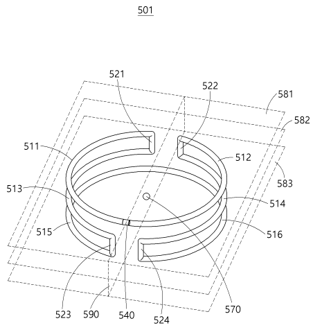
conductive wire and the second conductive wire are connected; and a feeder for
supplying a feed signal via the antenna port.
[0008] In the antenna device according to an embodiment, a combination of one
LEGAL 37504902.1 2
Date Recue/Date Received 2021-11-10
CA 03139920 2021-11-10
or two of the first conductive wire, the second conductive wire, the third
conductive
wire, the fourth conductive wire, the fifth conductive wire, and the sixth
conductive
wire may have a length of 1/4 of the wavelength of a target frequency.
[0009] In the antenna device according to an embodiment, the first area, the
second area, and the third area may be either polygonal or circular.
[0010] In the antenna device according to an embodiment, the first area, the
second area, and the third area may be equal in size and shape when viewed
from
a direction perpendicular to the first plane.
[0011] In the antenna device according to an embodiment, the first connection
part
and the second connection part may be disconnected from each other, and the
third
connection part and the fourth connection part may be disconnected from each
other.
[0012] In the antenna device according to an embodiment, a virtual straight
line
from the feeder to the first connection part may be at a threshold angle or
lower with
respect to the virtual plane, and a virtual straight line from the feeder to
the second
connection part may be at a threshold angle or lower with respect to the
virtual
plane.
[0013] In the antenna device according to an embodiment, conductive wires
disposed in a reference plane positioned halfway through a plurality of planes
parallel to and spaced apart from each other may generate a resonance by a
magnetic dipole, in response to a feed signal.
[0014] In the antenna device according to an embodiment, conductive wires
disposed in one or more planes positioned on one side of the reference plane
may
generate a resonance by a first electric dipole in response to the feed
signal, and
conductive wires disposed in one or more planes positioned on the other side
of the
reference plane may generate a resonance by a second electric dipole of the
opposite polarity to the first electric dipole in response to the feed signal.
LEGAL 37504902.1 3
Date Recue/Date Received 2021-11-10
CA 03139920 2021-11-10
[0015] In the antenna device according to an embodiment, the connection parts
may connect between the conductive wires through via holes.
[0016] In the antenna device according to an embodiment, the fifth conductive
wire
and the sixth conductive wire may be electrically connected to each other.
[0017] The antenna device may further include one or more conductive wires
electrically connected to the fifth conductive wire and the sixth conductive
wire,
which are disposed along a part of the boundary of an area in one or more
additional planes parallel to and spaced apart from the third plane while
being
spaced apart from each other.
[0018] In the antenna device according to an embodiment, the conductive wires
of
the antenna device may be printed on a surface of a printed circuit board
(PCB)
having the shape of a cylinder.
[0019] In the antenna device according to an embodiment, a resonance frequency
of the antenna device may vary in response to changes in the concentration of
a
target analyte around the antenna device.
[0020] The antenna device may further include a communication part for sending
to an external device biological parameter data regarding variations of the
resonance frequency of the antenna device and measured scattering parameters.
[0021] In the antenna device according to an embodiment, when a feed signal is
fed to the antenna device, the first conductive wire capacitively couples with
the
third conductive wire, the third conductive wire capacitively couples with the
fifth
conductive wire, the second conductive wire capacitively couples with the
fourth
conductive wire, and the fourth conductive wire capacitively couples with the
sixth
conductive wire.
[0022] An antenna device according to another embodiment may include: first
conductive wires disposed along a part of a first area in a first plane;
second
conductive wires which are disposed along a part of a second area in a second
LEGAL 37504902.1 4
Date Recue/Date Received 2021-11-10
CA 03139920 2021-11-10
plane parallel to and spaced apart from the first plane, and which
capacitively
couple with the first conductive wires; and third conductive wires which are
disposed
along a part of a third area in a third plane parallel to and spaced apart
from the
second plane, and which capacitively couple with the second conductive wires,
wherein the first conductive wires are connected to an antenna port and
connected
to the second conductive wires at a distal end relative to the antenna port,
and the
second conductive wires are connected to the third conductive wires at a
proximal
end relative to the antenna port, and a resonance generated by a magnetic
dipole
and a resonance generated by an electric dipole are formed separately in
response
to a feed signal fed to the antenna port.
[0023] An antenna device according to another embodiment may include: a first
conductive wire which is disposed in a reference plane positioned halfway
through a
plurality of planes parallel to and spaced apart from each other, and which
generates a resonance by a magnetic dipole; a second conductive wire which is
disposed in one or more planes positioned on one side of the reference plane,
and
which generates a resonance by a first electric dipole in response; and a
third
conductive wire which is disposed in one or more planes positioned on the
other
side of the reference plane, and which generates a resonance by a second
electric
dipole of the opposite polarity to the first electric dipole.
BRIEF DESCRIPTION OF THE DRAWINGS
[0024] FIG. 1 shows a general shape of a dipole antenna.
[0025] FIG. 2 shows an antenna element having a loop shape.
[0026] FIG. 3 shows an antenna element with two dipole antennas disposed
adjacent to each other.
[0027] FIG. 4 shows frequency response characteristics for electromagnetic
waves
according to the type of the antenna element.
LEGAL 37504902.1 5
Date Recue/Date Received 2021-11-10
CA 03139920 2021-11-10
[0028] FIG. 5A explains the shape of an antenna device according to an
embodiment.
[0029] FIG. 5B explains the direction of current flowing through an antenna
device
according to an embodiment.
[0030] FIG. 6 explains the shape of an antenna device according to an
embodiment.
[0031] FIG. 7 shows a cylindrical sensor including an antenna device according
to
an embodiment.
[0032] FIG. 8 shows a PCB-type sensor including an antenna device according to
an embodiment of the present disclosure.
[0033] FIGS. 9A and 9B show the shape of an in-body biosensor including an
antenna device according to an embodiment.
[0034] FIGS. 10A to 10C show frequency response characteristics for
electromagnetic waves according to the type of the sensor.
[0035] FIG. 11A explains how the resonance frequency of an antenna device
according to an embodiment varies with the concentration of a target analyte
around
the antenna device.
[0036] FIG. 11B shows how resonance frequency varies with relative dielectric
constant.
[0037] FIGS. 12A to 12C show frequency response characteristics for a magnetic
dipole and an electric dipole.
[0038] FIG. 13 shows frequency response characteristics for electromagnetic
waves.
[0039] FIG. 14 is a block diagram showing a glucose measurement system
according to an embodiment.
BEST MODE FOR THE INVENTION
[0040] Hereinafter, exemplary embodiments will be described in detail with
LEGAL 37504902.1 6
Date Recue/Date Received 2021-11-10
CA 03139920 2021-11-10
reference to the accompanying drawings. However, since various changes may be
made to the embodiments, the scope of the rights of the patent application is
not
limited or limited by these embodiments. It should be understood that all
changes,
equivalents, or substitutes to the embodiments are included in the scope of
the
rights.
[0041] The terms used in the example embodiments have been used for the
purpose of explanation only, and the terms should not be interpreted as an
intention
of limiting the explanation. An expression of the singular number includes an
expression of the plural number unless clearly defined otherwise in the
context. In
the present specification, it should be understood that a term such as
"include" or
"have" is used to specify existence of a feature, a number, a step, an
operation, a
constituent element, a part, or a combination thereof described in the
specification,
but it does not preclude the possibility of the existence or addition of one
or more
other features, numbers, steps, operations, constituent elements, parts, or
combinations thereof.
[0042] Unless otherwise defined, all terms, including technical and scientific
terms,
used herein have the same meaning as commonly understood by one of ordinary
skill in the art to which example embodiments pertain. Terms, such as those
defined in commonly used dictionaries, should be interpreted as having
meanings
that are consistent with those in the context of the related art but are not
interpreted
as having ideal or excessively formal meanings unless clearly defined in the
present
application.
[0043] In addition, in the description with reference to the accompanying
drawings,
the same reference numerals are assigned to the same components regardless of
the reference numerals, and redundant descriptions thereof will be omitted. In
describing the embodiments, when it is determined that a detailed description
of
related known technologies may unnecessarily obscure the subject matter of the
LEGAL 37504902.1 7
Date Recue/Date Received 2021-11-10
CA 03139920 2021-11-10
embodiments, the detailed description thereof will be omitted.
[0044] In describing the components of the embodiment according to the present
invention, terms such as first, second, "A", "B", (a), (b), and the like may
be used.
These terms are merely intended to distinguish one component from another
component, and the terms do not limit the nature, sequence or order of the
components. When a component is described as "connected", "coupled", or
"linked" to another component, this may mean the components are not only
directly
"connected", "coupled", or "linked", but also are indirectly "connected",
"coupled", or
"linked" via a third component.
[0045] A component that has the same common function as a component included
in any one example embodiment will be described using the same name in other
example embodiments. Unless otherwise stated, the description set forth in any
one example embodiment may be applicable to other example embodiments, and a
detailed description will be omitted in an overlapping range.
[0046] According to an embodiment, a technology regarding an in-body biosensor
capable of semi-permanently measuring glucose is provided. The in-
body
biosensor may also be referred to as an invasive biosensor, an insertable
biosensor,
or an implantable biosensor. The in-body biosensor may be a sensor that senses
a target analyte using electromagnetic waves. For example, the in-body
biosensor
may measure biometric information associated with a target analyte.
Hereinafter,
the target analyte is a material associated with a living body, and may also
be
referred to as a biological material (analyte). For
reference, in the present
specification, the target analyte has been mainly described as glucose, but is
not
limited thereto. The biometric information is information related to a
biological
component of a subject, and may include, for example, a concentration, level,
etc.,
of an analyte. If the analyte is glucose, the biometric information may
include a
glucose level.
LEGAL 37504902.1 8
Date Recue/Date Received 2021-11-10
CA 03139920 2021-11-10
[0047] The in-body biosensor may measure biological parameters (hereinafter,
referred to as "parameters") associated with the above-described biological
component, and determine biometric information from the measured parameters.
In the present specification, the parameters may represent circuit network
parameters used to analyze a biosensor and/or a biosensing system.
Hereinafter,
for convenience of explanation, scattering parameters will be mainly described
as
an example, but the parameters set forth herein are not limited to them. As
the
parameters, for example, admittance parameters, impedance parameters, hybrid
parameters, and transmission parameters may be used. For the scattering
parameters, transmission coefficient and reflection coefficient may be used.
For
reference, the resonance frequency calculated from the above-described
parameters may be related to the concentration of the target analyte, and the
biosensor may predict glucose levels by detecting a change in the transmission
coefficient and/or the reflection coefficient.
[0048] The in-body biosensor may include a resonator assembly (e.g., an
antenna). Hereinafter, an example in which the resonator assembly is an
antenna
will be mainly described. The resonance frequency of the antenna may be
expressed as a capacitance component and an inductance component as shown in
Equation 1 below.
[0049] [Equation 1]
1
f = ____________________
27TAIU
[0050]
[0051] wherein f denotes the resonance frequency of an antenna included in the
biosensor using electromagnetic waves, L denotes the inductance of the
antenna,
and C denotes the capacitance of the antenna. The capacitance C of the antenna
may be proportional to a relative dielectric constant Eras shown in Equation 2
LEGAL 37504902.1 9
Date Recue/Date Received 2021-11-10
CA 03139920 2021-11-10
below.
[0052] [Equation 2]
C CC Er
[0053]
[0054] The relative dielectric constant Er of the antenna may be affected by
the
concentration of the target analyte around it. For
example, when an
electromagnetic wave passes through a material having a certain dielectric
constant, changes in amplitude and phase may occur in the transmitted
electromagnetic wave due to radio reflection and scattering. Since the degree
of
reflection and/or scattering of the electromagnetic wave varies depending on
the
concentration of the target analyte present around the biosensor, the relative
dielectric constant Er may also vary. This can be construed that a biological
capacitance is formed between the biosensor and the target analyte, due to a
fringing field generated by the electromagnetic wave radiated by the biosensor
including an antenna. Since the relative dielectric constant Er of the antenna
varies with changes in the concentration of the target analyte, the resonance
frequency of the antenna also varies. In other words, the concentration of the
target analyte may correspond to the resonance frequency.
[0055] According to an embodiment, the in-body biosensor may radiate
electromagnetic waves while sweeping the frequency and measure scattering
parameters for the radiated electromagnetic waves. The in-body biosensor may
determine a resonance frequency from the measured scattering parameters and
estimate a glucose level corresponding to the determined resonance frequency.
The in-body biosensor may be inserted into a subcutaneous layer and predict
the
level of glucose diffused from a blood vessel to interstitial fluid.
[0056] The in-body biosensor may estimate biometric information by identifying
the
amount of frequency transition in resonance frequency. For more accurate
LEGAL 37504902.1 10
Date Recue/Date Received 2021-11-10
CA 03139920 2021-11-10
measurement of resonance frequency, a quality factor may be maximized.
Hereinafter, an antenna structure with an improved quality factor in an
antenna
device used in a biosensor using electromagnetic waves will be described.
[0057] FIG. 1 shows a general shape of a dipole antenna.
[0058] A general dipole antenna 100 may include two straight conductive wires
connected to a feeder 120. The two straight conductive wires may be connected
via the feeder 120. A first conductive wire 111 and second conductive wire 112
of
the dipole antenna may be connected to the feeder 120 in a straight shape,
without
facing each other. Here, the straight shape may refer to a shape in which the
first
conductive wire 111 and second conductive wire 112 of the dipole antenna 100
extend in opposite directions.
[0059] The feeder 120 may supply a feed signal to the dipole antenna via a
port.
The feed signal is a signal that is fed to the dipole antenna, which may be an
oscillation signal that oscillates at a target frequency. The feeder 120 may
supply a
feed signal in such a way that the currents flow in the same direction through
the
first conductive wire 111 and second conductive wire 112 of the dipole antenna
having a straight shape. For example, the current in the first conductive wire
111
of the dipole antenna may flow in a direction 130 at a certain time point, and
the
current in the second conductive wire 112 of the dipole antenna may flow in
the
same direction 130. Also, at another time point, currents may flow in opposite
directions simultaneously through the first conductive wire 111 and second
conductive wire 112 of the dipole antenna.
[0060] An electric dipole may be formed by the current flowing through the
first
conductive wire 111 of the dipole antenna 100, and an electric dipole may be
likewise formed by the current flowing through the second conductive wire 112.
Since the currents flowing through the first and second conductive wires of
the
dipole antenna go in the same direction, the directions of electric dipole
moments of
LEGAL 37504902.1 11
Date Recue/Date Received 2021-11-10
CA 03139920 2021-11-10
the electric dipoles formed by the first and second conductive wires may be
the
same.
[0061] FIG. 2 shows an antenna element 200 having a loop shape.
[0062] The antenna element may have the shape of a closed loop. For example,
as shown in FIG. 2, the antenna element 200 may include a first conductive
wire
211, a second conductive wire 212, a third conductive wire 213, and a fourth
conductive wire 214 that are connected together and have a circular shape. The
first conductive wire 211 and the fourth conductive wire 214 may be disposed
opposite each other with respect to a virtual straight line 281 passing
through the
center point 270 of a circle and an antenna port 221, and the second
conductive
wire 212 and the third conductive wire 213 may be disposed opposite each other
with respect to the virtual straight line 281. Also, the first conductive wire
211 and
the second conductive wire 212 may be disposed opposite each other with
respect
to a virtual straight line 282 passing through the center point 270 of the
circle and
orthogonal to the virtual straight line 281, and the third conductive wire 213
and the
fourth conductive wire 214 may be disposed opposite each other with respect to
the
virtual straight line 282.
[0063] Moreover, the antenna element 200 may further include a feeder 221 for
supplying a feed signal to an antenna via a port. The feeder 221 may be
disposed
between the first conductive wire 211 and the fourth conductive wire 214.
Hereinafter, the direction of current flowing through each conductive wire
when a
feed signal is supplied to the antenna element 200 via the feeder 221 will be
described.
[0064] For example, the length of the first conductive wire 211, second
conductive
wire 212, third conductive wire 213, and fourth conductive wire 214 of the
antenna
element 200 may have a length of 1/4 of the wavelength of the frequency of the
feed
signal supplied from the feeder 221. While the feeder 221 is feeding a feed
signal
LEGAL 37504902.1 12
Date Recue/Date Received 2021-11-10
CA 03139920 2021-11-10
of a sinusoidal wave, the current flowing through a point corresponding to 1/4
of the
wavelength from the feeder 221 may have an intensity of 0 at a time point
where the
feeder 221 supplies a current with maximum intensity from the sinusoidal wave.
At
that time point, the current in the first conductive wire 211 may flow in a
direction
231, and the current in the fourth conductive wire 214 may flow in the
direction 231.
At the same time, alternating current power is applied from the feeder 221,
and the
length of each conductive wire is 1/4 of the wavelength corresponding to the
power.
Thus, the currents in the second conductive wire 213 and third conductive wire
213
may flow in a direction 232 which is the opposite direction of the direction
231. The
direction 231 may be counterclockwise, and the direction 232 may be clockwise.
As a result, it may be construed that, at that time point, an electric dipole
is formed
by the first conductive wire and the fourth conductive wire, and an electric
dipole is
formed by the second conductive wire and the third conductive wire.
[0065] FIG. 3 shows an antenna element 300 with two dipole antennas disposed
adjacent to each other.
[0066] The antenna device 300 may include a first dipole antenna and a second
dipole antenna. The first dipole antenna may include a first conductive wire
311
and a second conductive wire 312. The second dipole antenna may include a
third
conductive wire 313 and the fourth conductive wire 314. The first conductive
wire
311 of the first dipole antenna and the third conductive wire 313 of the
second
dipole antenna may be disposed in a first plane 381. The first conductive wire
311
and the third conductive wire 313 may be disposed opposite each other with
respect
to a virtual plane 390 perpendicular to the first plane 381. The virtual plane
390
may be disposed between the first dipole antenna and the second dipole
antenna.
Likewise, the second conductive wire 312 of the first dipole antenna and the
fourth
conductive wire 314 of the second dipole antenna may be disposed in a second
plane 382. The second conductive wire 312 and the fourth conductive wire 314
LEGAL 37504902.1 13
Date Recue/Date Received 2021-11-10
CA 03139920 2021-11-10
may be disposed opposite each other with respect to the virtual plane 390.
[0067] The first dipole antenna and the second dipole antenna each may have a
length equal to the wavelength of a target frequency. For example, FIG. 3
explains
an example in which the closed loop is circular, and the first conductive wire
311
and the second conductive wire 312 each may have a length of half the
wavelength
of the target frequency. Similarly, the third conductive wire 313 and the
fourth
conductive wire 314 each may have a length of half the wavelength of the
target
frequency.
[0068] In this specification, the target frequency is a frequency at which the
antenna device is desired to operate, for example, a frequency at which an
antenna
device inserted into the body is desired to resonate when the antenna device
forms
a biological capacitance for a target analyte with a given concentration
inside the
body.
[0069] The first dipole antenna may include a first feeder 321, and the second
dipole antenna may include a second feeder 322. The first dipole antenna may
have a folded shape by folding the antenna element having a closed-loop shape
shown in FIG. 2 in half. Likewise, the second dipole antenna may have a folded
shape as if by folding the antenna element having a closed-loop shape in half.
For
example, the first dipole antenna may have a folded shape as if by folding the
antenna element at points on the conductive wires that are a 1/4 wavelength
away
from the first feeder 321. The first conductive wire 311 and second conductive
wire
312 of the first dipole antenna are disposed parallel to each other in a plane
where
they are spaced apart from each other, and may be connected through connection
parts having via holes. For example, the first conductive wire 311 and the
second
conductive wire 312 may be symmetrical with respect to a virtual plane between
the
first plane 381 and the second plane 283, but are not limited to this.
Likewise, the
second dipole antenna may have a folded shape by folding the antenna element
at
LEGAL 37504902.1 14
Date Recue/Date Received 2021-11-10
CA 03139920 2021-11-10
points on the conductive wires that are a 1/4 wavelength away from the second
feeder 322.
[0070] The first feeder 321 may supply power to the first dipole antenna, and
the
second feeder 322 may supply power to the second dipole antenna. Hereinafter,
the direction of current flowing through each conductive wire when a feed
signal is
supplied to the antenna element 300 via the feeders 321 and 322 will be
described.
[0071] As explained above, it can be construed that, in the circular loop
shown in
FIG. 2, currents flow in opposite directions with respect to points on the
conductive
wires that are a 1/4 wavelength away from the feeder 221, at a time point
where the
feeder 221 supplies a current with maximum intensity. Accordingly, in a case
where the antenna element having a loop shape shown in FIG. 2 is folded as
shown
in FIG. 3, currents may flow in the same direction through the conductive
wires in
the antenna element having a folded loop shape, when viewed from a direction
perpendicular to the first plane 381. For example, currents may flow through
the
first conductive wire 311 and second conductive wire 312 of the first dipole
antenna
in a first circulation direction 331 (e.g., counterclockwise in FIG. 3), and
currents
may flow through the third conductive wire 313 and fourth conductive wire 314
of the
second dipole antenna in a second circulation direction 332 (e.g.,
counterclockwise)
which is the same direction of circulation as the first circulation direction
331.
[0072] For reference, the direction of current circulation in this
specification is a
direction of current flowing through conductive wires disposed on a virtual
closed
loop and/or a part of the virtual closed loop, in a plane of the antenna
element,
which may refer to a direction in which current circulates clockwise or
counterclockwise when viewed from a direction perpendicular to planes where
the
conductive wires are disposed. The clockwise or counterclockwise direction may
be reversed depending on whether the planes are viewed from above or below and
depending on the polarity of alternating current. For reference, the first
circulation
LEGAL 37504902.1 15
Date Recue/Date Received 2021-11-10
CA 03139920 2021-11-10
direction 331 and second circulation direction 332 of FIG. 3 may be clockwise
at a
time point where the feeders 321 and 322 feed a current with maximum intensity
at
which the polarity of the feed signal is positive.
[0073] In the first plane 381, currents flow in one direction through the
first
conductive wire 311 and third conductive wire 313 disposed corresponding in
shape
to a part of the closed loop, thereby forming a first magnetic dipole.
Likewise, in
the second plane 382, currents flow in one direction through the second
conductive
wire 312 and fourth conductive wire 314 disposed corresponding in shape to a
part
of the closed loop, thereby forming a second magnetic dipole. The directions
of
magnetic dipole moments of the first magnetic dipole and second magnetic
dipole
may be the same. Electromagnetic waves generated by the first magnetic dipole
and electromagnetic waves generated by the second magnetic dipole may generate
constructive interference.
[0074] A resonance generated by a magnetic dipole has a higher quality factor
than a resonance generated by an electric dipole, and the quality factor may
be
expressed by the following equation:
[0075] [Equation 3]
j. __________
(m. )
R C +
v
[0076] R
[0077] wherein Q is quality factor, RL is the value of loss resistance, and Rr
is the
value of radiation resistance.
[0078] FIG. 4 shows frequency response characteristics for electromagnetic
waves
according to the type of the antenna element.
[0079] Frequency response characteristics 400 show frequency response
characteristics for electromagnetic waves according to the type of the antenna
element. A frequency response characteristic for scattered electromagnetic
waves
LEGAL 37504902.1 16
Date Recue/Date Received 2021-11-10
CA 03139920 2021-11-10
may be obtained by measuring parameters while sweeping the frequency. As
shown in FIG. 4, the frequency response characteristic may be a reflection
coefficient among scattering parameters.
[0080] A first reflection coefficient curve 410 represents a frequency
response
characteristic for the straight dipole antenna shown in FIG. 1. A second
reflection
coefficient curve 420 represents a frequency response characteristic for an
antenna
element having the shape of a closed loop shown in FIG. 2. A third reflection
coefficient curve 430 represents a frequency response characteristic for the
antenna
element 300 forming a magnetic dipole shown in FIG. 3. The quality factor of
the
antenna element 300 forming a magnetic dipole may be relatively high.
[0081] FIG. 5A explains the shape of an antenna device 501 according to an
embodiment.
[0082] The antenna device 501 according to an embodiment may be a conductive
sensor. The antenna device 501 according to an embodiment may include: a first
conductive wire 511 and a second conductive wire 512 which are disposed along
a
part of the boundary of a first area in a first plane 581 while being spaced
apart from
each other; a third conductive wire 513 and a fourth conductive wire 514 which
are
disposed along a part of the boundary of a second area in a second plane 582
parallel to and spaced apart from the first plane 581 while being spaced apart
from
each other; and a fifth conductive wire 515 and a sixth conductive wire 516
which
are disposed along a part of the boundary of a third area in a third plane 583
parallel
to and spaced apart from the second plane 582 while being spaced apart from
each
other. The antenna device 501 may include a first connection part 521
connecting
a first end of the first conductive wire 511 to a first end of the third
conductive wire
513; a second connection part 522 connecting a first end of the second
conductive
wire 512 to a first end of the fourth conductive wire 514; a third connection
part 523
connecting a second end of the third conductive wire 513 to a second end of
the fifth
LEGAL 37504902.1 17
Date Recue/Date Received 2021-11-10
CA 03139920 2021-11-10
conductive wire 515; and a fourth connection part 524 connecting a second end
of
the fourth conductive wire 514 to a second end of the sixth conductive wire
516. In
this case, the first end may represent a distal end relative to an antenna
port, and
the second end may represent a proximal end relative to the antenna port.
[0083] In the antenna device 501 according to an embodiment, the second end of
the first conductive wire 511 and the second end of the second conductive wire
512
may be connected to an antenna port. The first conductive wire 511 and the
second conductive wire 512 may be disposed opposite each other with respect to
a
virtual plane 590 passing through the antenna port and the center point 570 of
the
first area and perpendicular to the first plane 581. The third conductive wire
513
and the fourth conductive wire 514 may be disposed opposite each other with
respect to the virtual plane 590, and the fifth conductive wire 515 and the
sixth
conductive wire 516 may be disposed opposite each other with respect to the
virtual
plane 590. The fifth conductive wire 515 and the sixth conductive wire 516 may
be
electrically connected to each other.
[0084] The antenna device 501 according to an embodiment may further include
an antenna port to which the first conductive wire 511 and the second
conductive
wire 512 are connected and a feeder 540 for supplying a feed signal via the
antenna
port. The feeder 540 may cause a current to flow through each conductive wire
by
supplying power to the antenna device. When a feed signal is fed to the
antenna
device 501 according to an embodiment, the first conductive wire 511 may
capacitively couple with the third conductive wire 513, the third conductive
wire 513
may capacitively couple with the fifth conductive wire 515, the second
conductive
wire 512 may capacitively couple with the fourth conductive wire 514, and the
fourth
conductive wire 514 may capacitively couple with the sixth conductive wire
516.
[0085] To sum up, the antenna device 501 according to an embodiment may
include a first conductive wire 511 and a second conductive wire 512 which are
LEGAL 37504902.1 18
Date Recue/Date Received 2021-11-10
CA 03139920 2021-11-10
disposed along a part of a first area in the first plane 581, a third
conductive wire
513 and a fourth conductive wire 514 which are disposed along a part of a
second
area in the second plane 582 parallel to and spaced apart from the first plane
581,
and which capacitively couple with the first conductive wire 511 and the
second
conductive wire 512, and a fifth conductive wire 515 and a sixth conductive
wire 516
which are disposed along a part of a third area in the third plane 583
parallel to and
spaced apart from the second plane 582, and which capacitively couple with the
third conductive wire 513 and the fourth conductive wire 514.
[0086] In the antenna device 501 according to an embodiment, a combination of
one or two of the first conductive wire 511, the second conductive wire 512,
the third
conductive wire 513, the fourth conductive wire 514, the fifth conductive wire
515,
and the sixth conductive wire 516 may have a length of 1/4 of the wavelength
of a
target frequency. For
example, the first conductive wire 511, the second
conductive wire 512, the third conductive wire 513, the fourth conductive wire
514,
the fifth conductive wire 515, and the sixth conductive wire 516 may have a
length of
1/4 of the wavelength.
[0087] Here, the wavelength of the target frequency may represent a guide
wavelength. The relationship between the wavelength in air and the guide
wavelength may be given by the following Equation 4.
[0088] [Equation 4]
=
V. [0089] Er
[0090] wherein Ag is the guide wavelength, is the
wavelength in air, and Er is
the dielectric constant of a guide medium.
[0091] Since the antenna device 501 according to an embodiment forms
capacitive
coupling between the conductive wires, the wavelength of the target frequency
may
vary with the dielectric constant of a guide material. For example, since the
length
LEGAL 37504902.1 19
Date Recue/Date Received 2021-11-10
CA 03139920 2021-11-10
of each conductive wire of the antenna device 501 is 1/4 of the wavelength of
the
target frequency, the length of the conductive wires of the antenna device may
be
decreased by increasing the dielectric constant of the guide medium.
[0092] In the antenna device 501 according to an embodiment, the first area,
the
second area, and the third area may be either polygonal or circular. For
example,
if the first area is circular as shown in FIG. 5A, the first conductive wire
511 and the
second conductive wire 512 may be disposed corresponding in shape to a part of
the circumference in the first plane 581. If the second area is circular, the
third
conductive wire 513 and the fourth conductive wire 514 may be disposed
corresponding in shape to a part of the circumference in the second plane 582.
If
the third area is circular, the fifth conductive wire 515 and the sixth
conductive wire
516 may be disposed corresponding in shape to a part of the circumference in
the
third plane 583. For another example, if the first area is polygonal unlike in
FIG. 5A,
the first conductive wire 511 and the second conductive wire 512 may be
disposed
corresponding in shape to a part of the polygon in the first plane 581. For
example,
the radius of the first area, second area, and third area may be, but not
limited to,
2.4 mm, and the distance between the first area and the third area may be, but
not
limited to, 0.6 mm.
[0093] Furthermore, the first area, the second area, and the third area may
have a
closed loop shape, and the conductive wires may be disposed corresponding in
shape to the areas.
[0094] In the antenna device 501 according to another embodiment, the first
area,
the second area, and the third area may be equal in size and shape when viewed
from a direction perpendicular to the first plane 581.
[0095] The antenna device 501 according to one embodiment may supply power
to the conductive wires by using one antenna port. The antenna device 501 may
include conductive wires connected together by connection parts. Power may be
LEGAL 37504902.1 20
Date Recue/Date Received 2021-11-10
CA 03139920 2021-11-10
supplied to the conductive wires by using one port. For example, an electrical
path
may be formed which sequentially connects the first conductive wire 511, third
conductive wire 513, fifth conductive wire 515, sixth conductive wire 516,
fourth
conductive wire 514, and second conductive wire 512, from a first terminal of
the
antenna port to a second terminal of the antenna port.
[0096] For example, the first end of the first conductive wire 511 and the
first end
of the second conductive wire 512 may be disconnected from each other. The
first
conductive wire 511 may be connected to the first connection part 521, and the
second conductive wire 512 may be connected to the second connection part 522.
The first connection part 521 and the second connection part 522 may be
disconnected from each other. Likewise, the third connection part 523 and the
fourth connection part 524 may be disconnected from each other. A virtual
straight
line from the feeder 540 to the first connection part 521 may be at a
threshold angle
or lower with respect to the virtual plane 590. A virtual straight line from
the feeder
540 to the second connection part 522 may be at a threshold angle or lower
with
respect to the virtual plane 590. The first connection part 521 and the second
connection part 522 may be disposed symmetrically with respect to the virtual
plane
590. For example, a virtual straight line from the feeder 540 to the first
connection
part 521 may be at an angle of 5 degrees with respect to the virtual plane
590, and
a virtual straight line from the feeder 540 to the second connection part 522
may be
at an angle of 5 degrees with respect to the virtual plane 590.
[0097] FIG. 5B explains the direction of current flowing through an antenna
device
according to an embodiment.
[0098] The first conductive wire 511, second conductive wire 512, third
conductive
wire 513, fourth conductive wire 514, fifth conductive wire 515, and sixth
conductive
wire 516 of the antenna device 502 shown in FIG. 5A may have a length of 1/4
of
the wavelength of a target frequency. The feeder 540 of the antenna device may
LEGAL 37504902.1 21
Date Recue/Date Received 2021-11-10
CA 03139920 2021-11-10
supply power (e.g., a feed signal) to the antenna device 502. FIG. 5B shows
that
the conductive wires of the antenna device 502 shown in FIG. 5A are unfolded
in a
plane in order to interpret the direction of current. For
reference, in this
specification, it is construed that the direction of current and/or the
direction of
circulation is reversed if the current has opposite polarity.
[0099] FIG. 5B shows a current graph of a time point at which the intensity of
current flow is zero at a point 1/8 wavelength away from the feeder 540.
Hereinafter, the direction of current flowing through each conductive wire at
that
time point will be described. The current may flow clockwise in a conductive
wire
region from the feeder 540 to the point 1/8 wavelength away from it
(hereinafter, '1/8
wavelength point'). It may be construed that, since the polarity of current is
reversed at the 1/8 wavelength point, the direction of circulation is reversed
too.
The current may flow counterclockwise in a conductive wire region from the 1/8
wavelength point to a point 5/8 wavelength away from it (hereinafter, '5/8
wavelength point'). It may be construed that, since the polarity of current is
reversed again at the 5/8 wavelength point, the direction of circulation is
reversed
again too. The current may flow clockwise in a conductive wire region from the
5/8 wavelength point to a point 3/4 wavelength away from it (hereinafter, '3/4
wavelength point').
[00100] Accordingly, since a current flows in one circulation direction
(counterclockwise in FIG. 5B) in the second area defined by the third
conductive
wire 513 and the fourth conductive wire 514, a resonance generated by a
magnetic
dipole may be generated due to a circulating current flowing through the third
conductive wire 513 and the fourth conductive wire 514. Also, since a current
flows
in a line of symmetry with respect to the 1/8 wavelength point in the first
area
defined by the first conductive wire 511 and the second conductive wire 512,
the
current may be construed as flowing in the same direction, i.e., a first
linear direction
LEGAL 37504902.1 22
Date Recue/Date Received 2021-11-10
CA 03139920 2021-11-10
(e.g., upward from below in FIG. 5B). In other words, the first conductive
wire 511
and the second conductive wire 512 may operate as dipole antennas through
which
current flows in the first linear direction, and may generate a resonance by a
first
electric dipole. Similarly, since a current flows in a line-symmetric shape
with
respect to the 5/8 wavelength point, it may be construed that the current
flows in a
second linear direction (e.g., downward from above in FIG. 5B) opposite to the
first
linear direction. In other words, the fifth conductive wire 515 and the sixth
conductive wire 516 may operate as dipole antennas through which current flows
in
a second linear direction, and may generate a resonance by a second electric
dipole.
The first electric dipole and the second electric dipole may have electric
dipole
moments of opposite polarities.
[00101] To sum up, in the antenna device according to an embodiment,
conductive
wires disposed in a reference plane positioned halfway through a plurality of
planes
parallel to and spaced apart from each other may generate a resonance by a
magnetic dipole, in response to a feed signal. In the antenna device according
to
an embodiment, conductive wires disposed in one or more planes positioned on
one
side of the reference plane may generate a resonance by a first electric
dipole in
response to the feed signal, and conductive wires disposed in one or more
planes
positioned on the other side of the reference plane may generate a resonance
by a
second electric dipole of the opposite polarity to the first electric dipole
in response
to the feed signal.
[00102] As shown in FIG. 5A, the first electric dipole formed by the
conductive wires
in the first plane and the second electric dipole formed by the conductive
wires in
the third plane have opposite polarities, and therefore the resonances
generated by
the electric dipoles in the first and third planes may cancel out each other
in the
conductive wires in the second plane between the first and third planes. As
the
intensity of sinusoidal waves changes over time, the conductive wires in the
LEGAL 37504902.1 23
Date Recue/Date Received 2021-11-10
CA 03139920 2021-11-10
reference plane may repeatedly show an increase and decrease in the strength
of
the magnetic dipole formed by the current flowing in the first circulation
direction and
an increase and decrease in the strength of the magnetic dipole formed by the
current flowing in the second circulation direction. The conductive wires in
the
other planes may repeatedly show an increase and decrease in the strength of
the
electric dipole formed by the current flowing in the first linear direction
and the
second linear direction. In this case, electric dipoles of opposite polarities
may be
formed in planes positioned on opposite sides of the reference plane.
[00103] Accordingly, the antenna device 501 may form two resonances separately
by the first electric dipole and the second electric dipole, along with a
resonance
generated by a magnetic dipole with a high equality factor, in response to a
feed
signal fed to the antenna port. The antenna device 501 may show at least three
resonance frequencies.
[00104] FIG. 6 explains the shape of an antenna device according to an
embodiment.
[00105] According to an embodiment, the fifth conductive wire and the sixth
conductive wire may be electrically connected to each other. For example, the
first
end of the fifth conductive wire of the antenna device and the first end of
the sixth
conductive wire may be connected together. In the above, FIG. 5A explains an
example in which the fifth end of the fifth conductive wire of the antenna
device and
the first end of the sixth conductive wire are physically and directly
connected, and
FIG. 6 explains an example in which they are indirectly connected via an
additional
conductive wire.
[00106] For example, an antenna device 600 may further include an additional
conductive wire in addition to the antenna device 501 of FIG. 5A. The antenna
device 600 may further include a seventh conductive wire 631 and an eighth
conductive wire 632 which are disposed along a part of the boundary of a
fourth
LEGAL 37504902.1 24
Date Recue/Date Received 2021-11-10
CA 03139920 2021-11-10
area in a fourth plane 684 parallel to and spaced apart from the third plane
while
being spaced apart from each other, and a ninth conductive wire 633 and a
tenth
conductive wire 634 which are disposed along a part of the boundary of a fifth
area
in a fifth plane 685 parallel to and spaced apart from the fourth plane while
being
spaced apart from each other. Further, the antenna device 600 according to an
embodiment may further include a fifth connection part 651 connecting a first
end of
the fifth conductive wire to a first end of the seventh conductive wire; a
sixth
connection part 652 connecting a first end of the sixth conductive wire 653 to
a first
end of the eighth conductive wire 632; a seventh connection part 653
connecting a
second end of the seventh conductive wire 631 to a second end of the ninth
conductive wire 633; and an eighth connection part 654 connecting a second end
of
the eighth conductive wire 632 to a second end of the tenth conductive wire
634.
[00107] However, the antenna device according to an embodiment is not limited
to
this but may further include conductive wires which are disposed along a part
of the
boundary of an area in one or more additional planes parallel to and spaced
apart
from the third plane while being spaced apart from each other, as is the case
for the
antenna device 600. For example, the antenna device may include conductive
wires disposed in (2n+1) planes parallel to and spaced apart from each other,
in
order to form a resonance frequency by a magnetic dipole. Here, n may denote a
natural number equal to or greater than 1. In this case, the length of the
conductive wires may be, but not limited to, 1/4 of the wavelength. The length
of
the conductive wires may be slightly different from 1/4 of the wavelength.
[00108] FIG. 7 shows a cylindrical sensor including an antenna device
according to
an embodiment.
[00109] The cylindrical sensor 700 may be a sensor that has an antenna device
710
according to an embodiment printed on a surface of a printed circuit board
(PCB)
760 having the shape of the side of a cylinder. For example, the antenna
device
LEGAL 37504902.1 25
Date Recue/Date Received 2021-11-10
CA 03139920 2021-11-10
710 may be the antenna device shown in FIG. 5A. For example, the printed
circuit
board 760 may have the shape of a hollow cylinder. The conductive wires and
connection parts of the antenna device 710 may be printed on the printed
circuit
board. The connection parts may be comprised of conductive wires as well. For
another example, the cylindrical sensor 700 may be fabricated by printing the
conductive wires and connection parts of the antenna element on a flat
flexible
printed circuit board (FPCB) and rolling the antenna element into a
cylindrical shape
so that the terminals of the antenna port are disposed adjacent to each other.
[00110] FIG. 8 shows a PCB-type sensor including an antenna device according
to
an embodiment of the present disclosure.
[00111] FIG. 8 shows a PCB-type sensor 800 that has an antenna device 810
according to an embodiment printed on a multilayered printed circuit board
(PCB)
870. For example, the antenna device 810 may be the antenna device shown in
FIG. 5.
[00112] The first conductive wire and second conductive wire of the antenna
device
may be disposed on a first side 881 of the printed circuit board 870, and the
fifth
conductive wire and the sixth conductive wire may be disposed on a second side
882 opposite to the first side 881. Also, the third conductive wire and the
fourth
conductive wire may be disposed on a third side 883 between the first side 881
and
the second side 882. Each side may be made of a layer. The first connection
part, second connection part, third connection part, and fourth connection
part of the
antenna device 810 may connect between the conductive wires through via holes.
[00113] The first conductive wire and second conductive wire of the antenna
device
810 according to an embodiment may be connected to the antenna port. The
antenna port may be connected to a coaxial cable 890. The coaxial cable 890
may
include an inner conductor 891 and an outer conductor 892. For example, the
inner conductor 891 may be connected to the second end of the first conductive
LEGAL 37504902.1 26
Date Recue/Date Received 2021-11-10
CA 03139920 2021-11-10
wire of the antenna device 810, and the outer conductor 892 may be connected
to
the second end of the second conductive wire of the antenna device 810. The
coaxial cable may supply power to the antenna device 810 using the inner
conductor 891 and the outer conductor 892. For example, the second end of the
first conductive wire may be an input port of the antenna port, and the second
end of
the second conductive wire may be an output port of the antenna port.
[00114] FIGS. 9A and 9B show the shape of an in-body biosensor including an
antenna device according to an embodiment.
[00115] FIG. 9A may show a perspective view of the sensor according to an
embodiment. FIG. 9B may show a front view of the sensor according to an
embodiment.
[00116] A PCB-type sensor 900 including an antenna device according to an
embodiment may sense a target analyte by using electromagnetic waves in the
body. FIGS. 9A and 9B show a testing device 901 that holds water around the
PCB-type sensor 900 in order to conduct testing. In the
testing device 901, the
PCB-type sensor 800 of FIG. 8 may be contained in a cylindrical inner space
992.
A cylindrical space 991 having a larger diameter than the cylindrical inner
space 992
may surround the cylindrical inner space 992. In the testing device 901, a
change
in dielectric constant caused by a temperature change may be observed.
[00117] FIGS. 10A to 10C show frequency response characteristics for
electromagnetic waves according to the type of the sensor.
[00118] A frequency response characteristic for a scattered electromagnetic
field
may be obtained by measuring parameters while sweeping the frequency. The
frequency response characteristic may be a reflection coefficient among
scattering
parameters. A frequency response characteristic 1001 of FIG. 10A may represent
a frequency response characteristic for electromagnetic waves obtained by the
conductive wire-type sensor 501. A frequency response characteristic 1002 of
FIG.
LEGAL 37504902.1 27
Date Recue/Date Received 2021-11-10
CA 03139920 2021-11-10
1 OB may represent a frequency response characteristic for electromagnetic
waves
obtained by the PCB-type sensor 800. A frequency response characteristic 1003
of FIG. 10C may represent a frequency response characteristic for
electromagnetic
waves obtained by the sensor 901 of FIG. 9A. A resonance frequency may be
obtained by a frequency response characteristic, and the resonance frequency
may
refer to a frequency that exhibits a lower reflection coefficient than
frequencies
around it.
[00119] FIG. 11A explains how the resonance frequency of an antenna device
according to an embodiment varies with the concentration of a target analyte
around
the antenna device.
[00120] The antenna device according to an embodiment may include conductive
wires 1111 and 1112 spaced apart from each other. For example, the conductive
wire 1111 may correspond to the first connection part 521 of the antenna
device 501
shown in FIG. 5A, and the conductive wire 1112 may correspond to the second
connection part 522. However, this is merely an example given for convenience
of
explanation, and other connection parts spaced apart from each other may be
described in a similar way.
[00121] For example, a strong electric field may be generated between the
conductive wire 1111 and the conductive wire 1112. In other words, capacitive
coupling may be formed between the conductive wire 1111 and the conductive
wire
1112. On the contrary, a fringing field with a relatively low electric field
intensity
may be formed in a three-dimensional space around the conductive wire 1111 and
the conductive wire 1112. If a target analyte is located in the fringing field
around
the antenna device, a biological capacitance between the sensor and the target
analyte may change. As a result, the relative dielectric constant Erof the
antenna
varies with changes in the concentration of the target analyte around the
antenna,
and the resonance frequency of the antenna also may vary. Accordingly, it is
LEGAL 37504902.1 28
Date Recue/Date Received 2021-11-10
CA 03139920 2021-11-10
possible to calculate the concentration of the target analyte by measuring the
variation in the resonance frequency of the antenna.
[00122] FIG. 11B shows how resonance frequency varies with relative dielectric
constant.
[00123] A graph 1110 represents a resonance frequency generated by a magnetic
dipole. In the graph 1110, the resonance frequency may decrease as the
relative
dielectric constant of the target analyte around the antenna device increases.
A
graph 1120 represents a resonance frequency generated by an electric dipole.
In
the graph 1120, the resonance frequency may decrease as the relative
dielectric
constant of the target analyte around the antenna device increases. However,
the
amount of transition in the resonance frequency generated by the magnetic
dipole
and the amount of transition in the resonance frequency generated by the
electric
dipole become different as the relative dielectric constant increases. For
example,
the difference in resonance frequency between the magnetic dipole and the
electric
dipole decreases as the relative dielectric constant of the target analyte
increases.
[00124] FIGS. 12A to 12C show frequency response characteristics for a
magnetic
dipole and an electric dipole.
[00125] A sensor including an antenna device according to an embodiment may
generate resonances separately for a magnetic dipole and an electric dipole.
FIGS.
12A to 12C show frequency response characteristics according to the shape of
the
sensor. A frequency response characteristic for each dipole may be obtained by
measuring each dipole's moment while sweeping the frequency. The frequency
response characteristic may represent the intensity of the moment. Frequency
response characteristics 1201 of FIG. 12A may represent frequency response
characteristics for a dipole for the conductive wire-type sensor 501. A graph
1211
and a graph 1212 may represent frequency response characteristics for an
electric
dipole, and a graph 1221 and a graph 1222 may represent frequency response
LEGAL 37504902.1 29
Date Recue/Date Received 2021-11-10
CA 03139920 2021-11-10
characteristics for a magnetic dipole. Frequency response characteristics 1202
of
FIG. 12B may represent frequency response characteristics for a dipole for the
PCB-type sensor 800. A graph 1213 and a graph 1214 may represent frequency
response characteristics for an electric dipole, and a graph 1223 and a graph
1224
may represent frequency response characteristics for a magnetic dipole.
Frequency response characteristics 1203 of FIG. 12C may represent frequency
response characteristics for a dipole for the sensor 901 of FIG. 9A. A graph
1215
and a graph 1216 may represent frequency response characteristics for an
electric
dipole, and a graph 1225 and a graph 1226 may represent frequency response
characteristics for a magnetic dipole.
[00126] FIG. 13 shows frequency response characteristics for electromagnetic
waves.
[00127] Frequency response characteristics 1300 may represent frequency
response characteristics for electromagnetic waves of an antenna device. A
frequency response characteristic for scattered electromagnetic waves may be
obtained by measuring parameters while sweeping the frequency. As shown in
FIG. 13, the frequency response characteristic may be a reflection coefficient
among scattering parameters. A first reflection coefficient curve 1310 may
represent a frequency response characteristic measured by the PCB-type sensor
800. For example, a resonance frequency may be generated at 4.387 GHz and
5.975 GHz on the first reflection coefficient curve 1310. A second reflection
coefficient curve 1320 may represent a frequency response characteristic
measured
via simulation. For example, a resonance frequency may be generated at 4.281
GHz and 5.996 GHz on the second reflection coefficient curve 1320.
[00128] FIG. 14 is a block diagram showing a glucose measurement system
according to an embodiment.
[00129] The glucose measurement system 1400 according to an embodiment may
LEGAL 37504902.1 30
Date Recue/Date Received 2021-11-10
CA 03139920 2021-11-10
include an in-body biosensor 1401 and an external device 1430. The in-body
biosensor 1401 may include a measuring part 1410 and a communication part
1420.
[00130] For example, the in-body biosensor 1401 shown in FIG. 14 may be placed
subcutaneously into a subject, and the external device 1430 may be placed
outside
the body of the subject.
[00131] The measuring part 1410 is an antenna element, which may include a
resonator assembly, for example, a resonant element. The antenna element
and/or the resonator assembly may have a structure of the antenna device shown
in
FIG. 7. The measuring part 1410 of the in-body biosensor 1401 may measure
biological parameters for the antenna device. The in-body biosensor 1401
placed
subcutaneously into the subject may generate a signal by sweeping the
frequency
within a preset frequency band and feed the generated signal to the resonant
element. The sensor 1401 may measure scattering parameters for the resonant
element to which a signal with varying frequency is supplied.
[00132] The communication part 1420 may send to the external device 1430 data
indicating the measured scattering parameters. Also, the communication part
1420
may receive power for generating a signal supplied to the measuring part 1410
by
using a wireless power transmission method. The communication part 1420 may
include a coil to wirelessly receive power or send data.
[00133] The external device 1430 may include a communication part 1431 and a
processor 1432. The communication part 1431 of the external device 1430 may
receive biological parameters from a glucose measurement device that measures
the biological parameters which change with biometric information associated
with a
target analyte. For example, the communication part 1431 may receive
biological
parameter data (e.g., scattering parameters and variations in resonance
frequency)
of the resonant element measured by the measuring part 1410. The processor
1432 of the external device 1430 may determine biometric information (e.g.,
glucose
LEGAL 37504902.1 31
Date Recue/Date Received 2021-11-10
CA 03139920 2021-11-10
levels) by using the received biological parameter data. The external device
1430
may also be referred to as a biometric information processing device. A
biometric
information processing device that determines information indicating glucose
levels
as biometric information may be referred to as a glucose determination device.
For
example, the processor 1432 of the external device 1430 may determine glucose
levels for a living body by using biological parameter data.
[00134] As explained above, the antenna element may represent three or more
resonance frequencies generated by an electric dipole and a magnetic dipole.
Accordingly, the glucose measurement system 1400 may determine biometric
information (e.g., glucose levels and variations in glucose levels) by
tracking
changes in each of the three or more resonance frequencies. For example, the
values of the three or more resonance frequencies may be mapped to each
glucose
level. For example, a look-up table in which resonance frequencies of 1 GHz,
1.25
GHz, and 1.5 GHz are mapped to a glucose level XX mg/dL may be stored. The
glucose measurement system 1400 may search the look-up table for glucose
levels
that match measured resonance frequencies. However, the determination of
glucose levels is not limited to the above method, but a variety of methods
may be
used according to design.
[00135] Moreover, an example in which the in-body biosensor 1401 transmits
biological parameters to the external device 1430 without processing them has
been
mainly described, but the present disclosure is not limited to this. For
example, the
in-body biosensor 1401 may further include its own processor, and the
processor of
the in-body biosensor 1401 may determine glucose levels. In this case, the
sensor
1401 may transmit the determined glucose levels to the external device via a
communication part. Also, an additional device (not shown) including a
processor
may be placed subcutaneously and establish human body communication with the
in-body biosensor 1401. In this case, the additional device (not shown) may
LEGAL 37504902.1 32
Date Recue/Date Received 2021-11-10
CA 03139920 2021-11-10
receive measured biological parameter data directly from the in-body biosensor
1401 to determine glucose levels. Also, the additional device (not shown) may
send the determined glucose levels to the external device 1430 from inside the
body
of the subject.
[00136] Although the above-mentioned embodiments have been described by
limited drawings, those skilled in the art may apply various technical
modifications
and alterations based on the above embodiments. For example, appropriate
results can be achieved although described techniques are carried out in a
different
order from a described method, and/or described elements are combined or mixed
in a different form from the described method, or replaced or substituted with
other
elements or equivalents.
[00137] Therefore, other implementations, other embodiments, and equivalents
to
patent claims belong to the scope of the patent claims to be described later.
LEGAL 37504902.1 33
Date Recue/Date Received 2021-11-10