Note: Descriptions are shown in the official language in which they were submitted.
WO 2020/256594
PCT/RU2020/050124
A METHOD FOR PRODUCING A SEMICONDUCTING FILM OF ORGANIC-
INORGANIC METAL-HALIDE COMPOUND WITH PEROVSKITE-LIKE
STRUCTURE
Field of the invention
This invention relates to the field of materials science, in particular, to a
method for
producing films of semiconducting material based on the organic-inorganic
metal-halide
compounds with perovskite-like structure, which can be used as a light-
absorbing layer in solar
cells, including thin-film, flexible and tandem solar cells, as well as can be
applied for
optoelectronic devices, in particular, light emitting diodes.
Background of the invention Several methods for the preparation of
semiconductor
films of light-absorbing materials with a perovskite-like structure are known
so far.
The preparation of a thin layer or film of perovskite CH3NH3PbI3 in one step
by applying
a solution of perovskite in organic mixed solvent on a substrate with a thin
layer by bringing it
into rotation at high speed around an axis perpendicular to layers plane is
described in the ref.
[Saliba M. et at. Incorporation of rubidium cations into perovskite solar
cells improves
photovoltaic performance /1 Science (80-.). 2016. Vol. 354, No 6309. P. 206-
2091 In this case,
the resulting perovskite film, integrated together with other layers in the
composition of the solar
cell, serves as a light-absorbing material. In particular, this article
describes the creation of a
perovskite solar cell consisting of five main functional layers applied onto a
glass substrate: a
transparent electrically conductive electrode (e.g. FTO), a electron transport
layer (e.g. TiO2
blocking layer), a light-absorbing layer (perovskite), and a hole transport
layer (e.g. Spiro
MeOTAD), reverse electrode (Au). Light is absorbed by perovskite layer, which
leads to the
formation of nonequilibrium charge carriers in it - electrons and holes
Further, the electrons and
holes migrate to the electron-transport and hole-transport layers,
respectively, and further to the
corresponding electrodes.
The disadvantage of the above method is the difficulty of perovskite layer
preparation from
a solution on large area substrates and, accordingly, the inability of large-
area perovskite solar
cells fabrication.
The known documents of particular relevance to the claimed invention are:
publication W02018124938A1 "Methods for producing light-absorbing materials
with
perovskite structure and liquid polyhalides of variable composition for their
implementation",
patent RU2685296 "method for producing a film of light-absorbing material with
a
perovskite-like structure",
and patent RU2675610 "a method for producing a film of a light-absorbing
material
with a perovskite-like structure".
CA 03140165 2021-11-30
WO 2020/256594
PCT/RU2020/050124
The method described in publication W02018124938A1 consists in mixing the
reagent of the composition AX - nX2, where n is greater than or equal to one,
while
component A is a singly charged organic or inorganic cation or a mixture
thereof,
component X2 is C12, Br2, 12 or mixture thereof, and a reagent containing B,
which is used
as a film of Sn, Pb or Di of a given thickness in the form of a metal or in
alloys, oxides,
salts. The reagent composition AX - nX2 is applied to the reagent B. The
reaction
proceeds: B + AX + X2 = ABX3, resulting in perovskite ABX3, excess reagents
are
removed if necessary.
A disadvantage of the known method is the impossibility of dosing a polyiodide
(polyhalide) reagent in amount which is stoichiometric with respect to
component B per unit area
of the film. The impossibility of dosing is a consequence of the high
reactivity and viscosity of
the liquid composition AX - nX2. The AX3/B ratio significantly (more than 5%)
different from
the stoichiometric one corresponding to pure ABX3 inevitably leads to a
deterioration in the
quality (in particular, uniformity of thickness and phase purity) of the
resulting film of a
semiconductor material, which negatively affects the efficiency of solar cells
based on obtained
films.
The method described in patent RU 2685296 Cl, consists in that a uniform layer
of
component B is formed on the substrate, a mixture of reagents that react with
component B
is prepared under predetermined conditions, and of a reaction inhibitor that
suppresses this
reaction under these conditions, the prepared mixture is applied in an amount
stoichiometric or greater than stoichiometric to the layer of component B and
the reaction
inhibitor is removed from the mixture, so that a chemical reaction between the
mixture of
reagents and component B is activated to form a film of perovskite-like
material (ABX3)
The above method allows the formation of a perovskite layer on surfaces of
virtually any
size. However, the disadvantage is low efficiency (not higher than 5%) of the
films obtained
using this method. [Stepanov NM, Petrov AA, Belich NA, Tarasov AB, Study of
the reactivity
of the ternary system MM - 12 - i-PrOH with metallic lead to obtain MAPbI3
films (MA
CH3NH3), abstracts at the conference XXV International Conference of Students,
Graduate
Students and Young Scientists "Lomonosov", Russia, April 9-13, 20181, [Rakita
Y. et al. Metal
to Halide Perovskite (HaP): An Alternative Route to HaP Coating, Directly from
Pb (0) or Sn (0)
Films // Chem Mater. 2017. Vol. 29, .NI=20 P 8620-8629]. This problem is a
consequence of the
fundamental flaws inherent in this method, in particular:
1) The precise control over the conditions and the rate of the process of the
formation of
the perovskite layer can hardly be achieved within the abovementioned method.
Accordingly, the
morphology and size of grains and crystallites of the resulting perovskite
film. This problem is
2
CA 03140165 2021-11-30
WO 2020/256594
PCT/RU2020/050124
caused by the high reactivity of the AX-nX2 composition of polyiodide melts
formed upon
removal of the inhibitor, as well as their increased recrystallization ability
with respect to the
perovskite layer.
2) Phase segregation during the formation of mixed-cation perovskites
containing
cesium and formamidinium (FA+) cations because the process of chemical
conversion at
low temperatures leads to the irreversible formation of non-perovskite low-
temperature
phases, for example, 5-CsPbI3, ö-FAPIth.
The method for producing a film of a light-absorbing material with a
perovskite-like
structure having the structural formula ADE3 (in the terminology of the
claimed invention,
component D is identical to component B, component E is identical to component
X)
disclosed in patent RU 2675610 is the most relevant to the claimed invention
in terms of
technical essence. This method is realizing by following: a layer of reagent D
and a layer of
reagent AE are successively applied to the substrate, after which the
substrate with the deposited
layers is placed in a liquid or gaseous medium containing reagent B2 for the
period necessary
and sufficient for the reaction to proceed: C + AE + E2 = ADE3 + X, with
CH3NH3+or
(NH2)2CI-1+ or C(NH2)3+ or Cs+ or a mixture thereof as component A, Cl or Br
is used as
component E or I or a mixture thereof, Sn, Pb or Bi metals or their alloys or
oxides or salts act as
component D, and X represents the decomposition product of component D when an
oxide or
salt is used as it.
The main disadvantage of the above method is the difficulty of controlling the
deposition
of a layer of reagent AE on the substrate surface with a layer of component D.
In particular, in
the case of organic cation A the deposition of the AE reagent thin layer by
gas-phase or thermal-
evaporative methods is difficult due to the possibility of their thermal
decomposition and
uncontrolled deposition in the regions of the substrate, on which its
deposition is undesirable or
unacceptable.
The use of vacuum deposition for the application of reagent AE, allows to
achieve the
dosage of reagent AE per unit area, however, requires the use of expensive
equipment.
In addition, the bilayer structure AE@D formed by any of the possible methods
exhibits an extremely high sensitivity to air moisture due to the high
moisture sensitivity
(hygroscopicity) of AE reagent. The latter requires the use of special
conditions, technical
means and solutions when handling the resulting bilayer structure
These two factors significantly reduce the technological advantages of this
method
for large-scale producing of perovskite thin films and devices based on them.
The terrninolon of the invention
3
CA 03140165 2021-11-30
WO 2020/256594
PCT/RU2020/050124
In the context of this invention, the perovskite-like structure means both the
perovskite
structure and any structures derived from perovskite structure. Accordingly,
the terms
"perovskite-like compounds" and "perovskite-like phases", as used herein,
refer to compounds
and phases with a perovskite-like structure respectively.
In particular, the term "halide perovskite" in the context of this invention
means phases
with the formula of ABX3 with cubic crystal system or any lower crystal system
(foe.g.
tetragonal, orthorhombic), as well as mixtures of different phases of halide
perovskites. The
structure of halide perovskites consists of a three-dimensional network of
comer connected
regular or distorted octahedra [BX6] consisting of a central atom ¨ component
B (cation Br') and
six X atoms (anions X").
In particular, "the perovskite-like structure" , as used herein, refer to the
set of structures of
so-called layered or two-dimensional or low-dimensional perovskite-related
compounds
containing layers of corner connected octahedra [BX.6] (perovskite layers),
alternating with
layers of another motif (for example, the Aurivillius phases, Ruddlesden-
Popper phases, Dion-
Jacobson phases) [Mitzi D.B. Synthesis, Structure, and Properties of Organic-
Inorganic
Perovskites and Related Materials // Progress in Inorganic Chemistry, Volume
48. Wiley Online
Library, 2007. P. 1-121]. The perovskite-like compounds and perovskite-like
phases are relate to
compounds and phases with a perovskite-like structure respectively.
The halide perovskite and the halide perovskite-like phases described above
belong to
complex halide salts comprising haloplumpates, halostannates and
halobismuthates (complex
metal-halide salts of lead, tin and bismuth respectively), therefore, in
general, such materials are
referred to as organic-inorganic metal-halide compounds with perovskite-like
structure.
The term "seeds", as used herein, refers to small grains or nuclei of
crystallites of the
perovskite-like phase with a size in any direction of no more than 100 ntn.
Disclosure of the invention
A technical problem is the need to overcome the disadvantages inherent in the
known
analogues and prototype by inventing a simpler and more technologically
advanced method for
producing semiconducting films of organic-inorganic metal-halide compounds
with perovskite-
like structure which can be used as a light-absorbing layer in the perovskite
solar cells to
increase their power conversion efficiency (PCE or efficiency) in comparison
with analogues.
The technical result achieved by using the claimed invention is to enable the
formation of
a film of a perovskite-like phase with increased average grain size in
comparison with related
methods due to the introducing of an intermediate step providing the formation
of a film
4
CA 03140165 2021-11-30
WO 2020/256594
PCT/RU2020/050124
comprising the seeds of the phase with a perovskite-like structure, as well as
the initial reagent
AX and precursor of component B (hereinafter "precursor B"), which ensures the
increase in the
efficiency (PCE) of the solar cells based on the obtained film of the
perovskite-like material as a
light-absorbing layer.
An additional technical result is improving of the electronic and optical
properties of
perovskite films obtained using the proposed method in comparison with related
methods
involving the reaction conversion of the component precursor B by the action
of reagents AX
and X2 into a organic-inorganic metal-halide compound with perovskite-like
structure
Another advantage of the proposed method is the possibility of its
implementation without
the use of specialized expensive equipment and complicated technical
requirements, which
makes the claimed method more relevant for use in industrial large-scale
production.
The formation at the intermediate step of the said film, comprising the seeds
of the phase
with a perovskite-like structure, as well as the initial reagent AX and
precursor B, is necessary
for increasing of the grain size in the resulting film of organic-inorganic
metal-halide compound
with perovskite or perovskite-like structure. An increase in the grain size
improves the electronic
and optoelectronic properties of the film of a polycrystalline semiconductor
material, in
particular, leads to a decrease in the recombination of charge carriers at
grain boundaries, which
leads to an increase in the efficiency (PCE) of devices based on the films of
the same material
with larger grains (see Table-1 in the section Examples of the invention).
When the said film,
comprising the seeds of the phase with a perovskite-like structure, as well as
the initial reagent
AX and precursor B, is treated by halogen the seeds grow consuming the initial
reagent AX and
precursor B and other seeds through a chemical reaction between the reagent
AX, precursor B
and X2 (e.g B + AX + X2 = ABX3) finally leading to the film of the perovskite-
like phase with
large grains (average size 500 nm or more) Treatment by halogen is carried out
at a given
temperature and a given partial pressure of halogen (or a given
concentration), which
provides the control of the chemical reaction rate and the grain size of the
perovskite film,
ensuring overcoming of the analogs and prototype disadvantages.
In the context of this invention, the chemical conversion means a chemical
processes
leading to the formation of halide perovskite ABX3 or a halide perovskite-like
compound of the
composition An+1n11X3n+1 where 1 < n < 100, as a result of the reaction
between the precursor of
component B (metal, alloy, oxide),reagent AX and reagent X2. In the general
case, the reaction
can be written by the following equation:
CA 03140165 2021-11-30
WO 2020/256594
PCT/RU2020/050124
nif + (n+1)AX + ((3n+1)/2)X2 = A11h1B11X30-hi + Y, where B' - is the precursor
of
component B, and Y ¨ is a by-product releasing in the cases of using an oxide
or salt as a
precursor of the component B.
The chemical conversion can occur as a result of both simultaneous addition of
components, and multiple sequential additions. In the context of this
invention, the full
chemical conversion of initial reagents (AX, X2) and precursors (B) into the
organic-
inorganic metal-halide compound with perovskite-like structure means that more
than 90%
(mole fraction) of the initial substances (reagents and precursors) have
reacted.
Brief description of the figures:
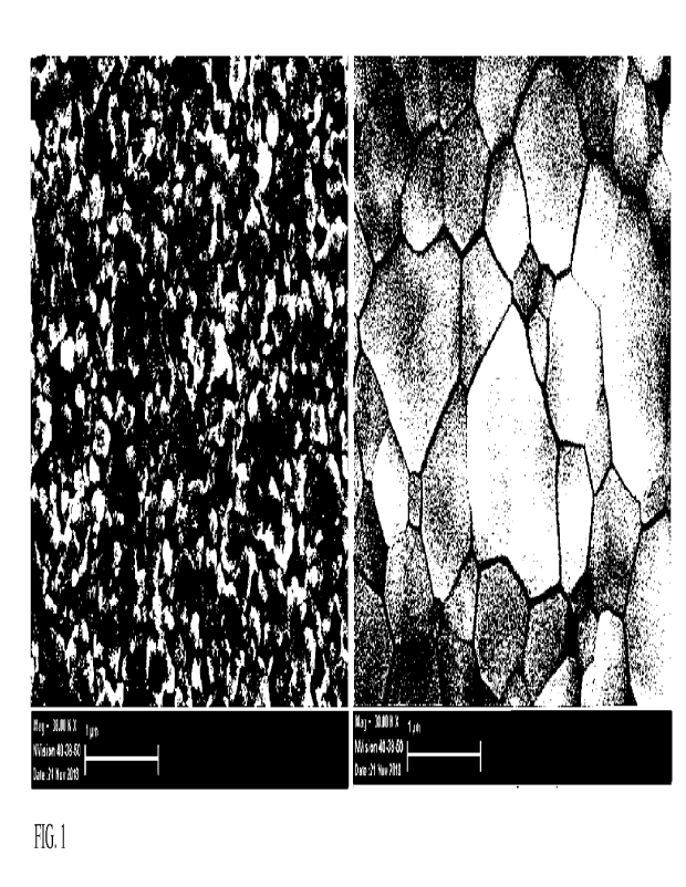
FIG. 1 shows micrographs of the top surface of the films using an scanning
electron
microscope (SEM). The FIG. 1 (a) (left) shows a micrograph of the surface of
the film obtained
after applying to the surface of metallic lead (a precursor of component B) a
solution containing
a mixture of reagents MAX and X2 with a ratio of [X2] / [MAX] = 0.5. On the
surface of the
perovskite grains MAPbI3 and MAI with a size of about 20-100 nm can be seen.
The FIG. 1
(b) (right) is a micrograph of the surface of the final perovskite film
obtained after treatment of
the film shown in FIG. 1 (a) by iodine (X2) vapours and after its full
chemical conversion to
perovskite MAPbI3 The resulting film contains crystallites ranging in size
from 200 nm to 1 pm
or more.
FIG. 2 shows a graph reflecting the dependences of the average grain size of
the resulting
MAPbI3 perovskite films and on the composition of the solution used to form
the intermediate
film in step II and the PCE (%) of solar cells, including films made using
these perovskite films
as a light-absorbing layer.
The detailed description of the invention
The described in this invention method of producing semiconducting film of the
organic-
inorganic metal-halide compounds with perovskite or perovskite-like structure
is a process
comprising the following main:
Step-I: the formation of the precursor layer of component B, where B = Pb, Sn,
Bi on the
surface of substrate.
Step-II: applying to the surface of the precursor layer of component B of the
composite
reagent containing a mixture of components A+ and X- with a molar ratio of 0+5
4 / [X-] <10
or reagent AX and reagent X2 with a molar ratio in the range 0 <[ X-] / [X2]
<1 or 0 <[X2] / [AX]
<1, respectively, with the formation of a film containing seeds of the
perovskite-like phase, as
well as components of the AX and B. This step can include an additional step
of post-processing
(heating, annealing, light irradiation) of the obtained film without changing
its chemical
composition.
6
CA 03140165 2021-11-30
WO 2020/256594
PCT/RU2020/050124
Step-III: treatment (exposure) of the previously formed film containing the
seeds of the
perovskite or perovskite-like phase, as well as reagent AX and the precursor
of component B, by
reagent X2, resulting in the formation of the semiconducting film of the
organic-inorganic metal-
halide compound with perovskite or perovskite-like structure or a film of
material with
composition identical to the target phase of the organic-inorganic metal-
halide compound with
perovskite or perovskite-like structure, or mixtures thereof. In the last two
cases, an auxiliary
step of post-processing of the film of the obtained material is introduced to
ensure the complete
conversion of any impurity phases of the film material into the target phase
of the organic-
inorganic metal-halide compound with perovskite or perovskite-like structure.
In the first step (step I), a precursor layer of component B is formed on the
surface of the
carrier substrate. In this case, glass, a transparent conductive silicon
oxide, a polymer, including
a transparent and conductive polymer, are used as the carrier substrate, and
any other material
inert with respect to the reagents used and the final material (perovskite
halide or perovskite-like
compound). It was experimentally shown that the physicochemical processes that
occur at all
three main steps of the proposed process do not depend on the nature of the
inert material of the
carrier substrate. Inert material in the terminology of the claimed invention
is any material that
does not enter into any chemical interactions with the final material, its
components, reagents
and solvents used in its synthesis. Hereinafter, we will call the substrate
material the material of
the upper layer of the substrate, directly onto which the precursor of
component B is applied.
In one embodiment of this invention, the carrier substrate material was chosen
identical to
the materials used in the construction of perovskite solar cells and similar
photovoltaic devices.
Typically, in such devices, an ABX3 layer is applied to the surface of a layer
of a transparent
electronically conductive material (transparent electrically conductive oxide,
electrically
conductive polymer) deposited on top of glass or a transparent polymer. In the
general case, it is
assumed that the carrier substrate contains all the functional layers
necessary to create the
finished device (solar cell, LED), except for the layer of light-absorbing
material ABX3 and
overlying functional layers.
In one embodiment of this invention, layers of lead, tin or bismuth with a
thickness of 5
nm to 500 nm were sprayed onto substrates of the following materials: fluorine-
doped tin oxide
(FTO) glass, doped with indium tin oxide (ITO), tin oxide SnO2 (on FTO , ITO)
or titanium
oxide TiO2 (planar and mesoporous layer), polyethyleneterephthalate,
polytriarylamine (PTAA)
Before applying the precursor layer of component B, the surface of the carrier
substrate is
thoroughly cleaned of contaminants. In particular, they are purified in an
aqueous solution of
surface-active substances (surfactants) using ultrasound, washed with
distilled water and purified
with ozone plasma.
7
CA 03140165 2021-11-30
WO 2020/256594
PCT/RU2020/050124
The precursor of component B is applied in the form of a metal film - Pb, Sn,
Bi or their
alloy or a layered structure containing several layers of metals (Pb, Sn, Bi)
located one on top of
the other. Also, salts and oxides of lead, for example, PbI2 and Pb0, can also
be used as a
precursor to component B.
The precursor of component B is applied by vacuum deposition, electrochemical
deposition, chemical vapor deposition, decomposition of a previously applied
solid phase
compound containing component B, or by other methods.
The most convenient and technologically advanced is the use of metal component
B as a
precursor. Methods for applying metal films of a given thickness are well
known, widely
distributed and available.
In one embodiment, the films of the precursor of component B in the form of a
metal (tin,
lead, bismuth) were deposited by thermal or magnetron sputtering in vacuum. At
the same time,
a cleaned substrate was placed in a vacuum chamber, fixed at a predetermined
distance from the
heating crucible or magnetron target, and sputtering was carried out with the
thickness of the
sprayed coating controlled by a quartz thickness sensor.
In the second step (step II), the composite reagent is applied to the surface
of the precursor
layer of component B, the composite reagent containing a mixture of components
A+ and X- with
a molar ratio of 0.5 <L ATM < 10 or reagent AX and reagent X2 with a molar
ratio in the
range 0 < [X-V[X2] < 1 or 0 < [X2]/[AX] < 1, respectively, with the formation
of a film
containing seeds of perovskite-like phase, as well as reagent AX and precursor
B.
The composite reagent containing reagent AX or a mixture of components A+ and
X-, as
well as reagent X2, is distributed in a uniform thin layer on the surface of
the precursor layer of
component B using inkjet printing, screen printing, spin-coating, and
immersion coating aerosol
spraying method, in particular, ultrasonic spraying, atomization through a
nozzle, electro-
spraying, aerosol inkjet printing or other methods.
As the composite reagent, a solution or a solvent diluted melt containing
cation At anion
X" and halogen X2, as well as a colloid or suspension or emulsion containing
these components
in a liquid or solid phase in a mixture with one or more solvents are used.
To add components A+ and X- to the composition of the composite reagent in the
necessary
stoichiomettic ratio, it is possible to use both the AX salt itself and any
mixture of salts, at least
one of which contains component At and any other component X- As a result of
mixing, both
components A-h and X- appear in the composition of the solution. In one
embodiment of this
inventionõ the composite reagent was prepared using acetates, formates,
fluorides, oxalates of
singly charged organic cations mixed with ammonium, potassium halides or with
hydrogen
8
CA 03140165 2021-11-30
WO 2020/256594
PCT/RU2020/050124
halides as an anion halide source, while the organic cation salt and anion
halide source were
taken in a ratio close to unit.
In one embodiment of this invention, methyl ammonium
iodide (CH3NH3I),
methylammonium bromide (CH3NH3Br), formamidinium iodide (FAD, formamidinium
bromide
(FABr), cesium iodide (Cs!) and various halide salts of substituted (primary,
secondary, tertiary,
or quaternary) ammonium cations and other stoichiometric halides with suitable
singly charged
cations were used as the AX salt.
For the successful implementation of the proposed method, the concentration of
reagents
AX and X2 in the applied composite reagent is selected in such a way as to
ensure the application
of component A in an amount stoichiometric with respect to component B per
unit area of the
film.
This condition is fulfilled, in particular, when a precursor component A of
reagent AX is
applied to the film surface in a stoichiometric amount per unit area of the
film. In this case, a
deviation of up to 10% from the optimal A/3 ratio for the resulting material
may be acceptable.
For 3D halide perovskites, the optimal ratio is A/B = 1, since it corresponds
to the
stoichiometry of the final material ABX3 and results in a single-phase film
after the conversion is
completed. For another perovskite-like compounds, this ratio may vary
depending on the desired
compound. In particular, it was shown that the ratio A/B = (n+1)/n is optimal
for layered halide
perovskites.
In one embodiment, the layered halide perovskites BA2Pb14, PEA214744, BDAPbh,
(BA + is
the butylammonium cation, PEA + is the phenylethylammonium cation, BDA2+ is
the
butanediammonium cation) were obtained with optimal A/B ratio about 2.
Analogously, the
optimal A/B ratios for any given perovskite-like compound can be easily
calculated according to
its chemical formula.
The most convenient and technically simple way to apply a given amount of
reagents AX
and X2 per unit area of the film of precursor B is to distribute their
solution over the surface of
the precursor layer of component B. In this case, acetone, alcohols,
tetrahydrofuran, dioxane,
acetonitrile or a mixture of these solvents are used as any ratio, it is also
possible to use any other
organic or inorganic neutral solvent. In this context, a neutral solvent is
any solvent that is not
able to dissolve the compounds of component B at a concentration of more than
0.3 M
In different embodiments of the invention, the composite reagent comprising
reagents AX
and X2 may be applied on the substrate by any means. Typically, to provide a
uniform
distribution of a thin layer of the reagents AX and X2 over the surface of a
substrate, the spin-
coating method is convenient, as it is fast and requires a small amount of
solution. Generally, in
9
CA 03140165 2021-11-30
WO 2020/256594
PCT/RU2020/050124
the case of the substrates of large area the composite reagent is applied on
the substrate by spin-
coating, spray-coating (aerosol spraying), slot-die coating or vapour
deposition.
To successfully realize the claimed method, it is necessary to obtain after
step-II a film not
only having A/B ratio corresponding to chemical formula of desired perovskite-
like compound,
but also containing seeds of perovskite-like phase (perovskite phase nuclei),
as well as residual
reagent AX and precursor B.
A fundamentally important condition for the formation of perovskite phase
nuclei is the
possibility of a chemical reaction of the reagent solution AX and X2 with the
precursor of
component B to form perovskite. In this case, only part of the initial
precursor of component B
should be subjected to chemical conversion into perovskite, and part of it
should remain
unchanged in order to react with an excess of the applied reagent AX during
treatment by
halogen in the next step (Ill) with the formation of perovskite.
The amount of perovskite-like phase in the form of seeds after the step-II is
determined by
the amount of halogen X2 in the applied composite reagent. For this, the
process is carried out
under such conditions in which only a chemical reaction (chemical conversion)
of the component
B precursor into perovskite occurs while it interacts with reagents AX and X2,
and perovskite
does not form when the component B precursor interacts with AX. These
conditions are realized,
since reagents AX and X2 together form a highly reactive polyiodide melt
[Petrov A.A. et al, A
new formation strategy of hybrid perovskites via room temperature reactive
polyiodide melts //
Mater. Horiz, 2017. Vol. N424. P. 625-6321 which reacts with the precursors of
component B
with the formation of perovskite in seconds or tens of seconds even at low
temperatures, while
the reaction of component B with reagent AX can proceed at a noticeable rate
only at elevated
temperatures or during the order of hours.
Therefore, in the case of applying a stoichiometric amount of AX to the
precursor of
component B, the amount of perovskite will be determined by the ratio
[X2]/[AX] or the
proportion of halogen ¨8.
Thus, the general equation for the chemical processes occurring in step II can
be written as
follows:
B' + AX + 5X2 ¨> 8ABX3 + (1-8)B" @AX + Yi
where B 'is the initial precursor of component B (usually in the form of a
metal), B"is the
final precursor of component B (neither perovskite nor perovskite-like
compound), usually
identical to the original precursor B', Y is a by-product (then can be removed
by post-
processing).
Pb + MM + 812 5MAPbI3 + (1-5)Pb@MAI
{Pbo sSno2)+ MM + 512 ¨ 45MAPbo sSno 213 + (1-5){Pbo FtSno 2)@MAI
CA 03140165 2021-11-30
WO 2020/256594
PCT/RU2020/050124
Pb + 2BAI + 612 ¨> SBA2Pbh+ (1-8)Pb@2BAI
In one embodiment of the invention, a solution of reagents AX and X2 in an
organic
solvent is applied to the surface of the component B precursor by spin-coating
(or spin-coating)
spinning coatings in an organic solvent to form a film containing nuclei of
grains of the halide
perovskite phase. In the process of spin-coating (disclosed, for example, in
- dissertations (http://konf x-pdf. ru/18fizika/632895-1-fotovoltaicheskie-
strukturi-osnove-
organicheskih-poluprovodnikov-kvantovih-tochek-cdse.php);
- GOST R ISO 27911-2015 "State system for ensuring the uniformity of
measurements
(GSI). Chemical analysis of the surface. Scanning probe microscopy.
Determination and
calibration of the lateral resolution of a near-field optical microscope"
(hap :fidocs. cntdsuidocument/1200119068);
- in https://www.msu.ruiscience/main
themes/v-mgu-razrabotali-novuyu-strategiyu-
polucheniya- perovskitnykh-solnechnykh-yacheek.html) the solution is
distributed on the surface
with an even thin layer, at the same time the evaporation of the solvent
begins, as a result, the
concentration of reagents AX and X2 in a thin layer above the film of the
precursor of component
B increases and a quick chemical reaction of AX and X2 with the precursor of
component B
begins. If the ratio [X21/[AX] is greater than 0 and less than 1, the result
is a film containing
nuclei of grains of the perovskite phase or perovskite-like phase, as well as
AX and B. The
formation of such a film is achieved in a time of the order of 5-100 seconds
when the process is
carried out at temperatures of 10-40 C. In the absence of X2, the formation of
perovskite under
these conditions does not occur, whereas when the ratio [X2HAX] is greater
than 1, the reaction
completely converts component 13 into the halide perovskite by the precursor.
Thus, the key step of the proposed method (the formation of a film containing
perovskite
or perovskite-like phase nuclei, as well as reagent AX and precursor B) can be
realized if the
ratio [X2]/[AX] lies in the range greater than 0 and less than 1, with this
optimal ratio is close to
0.5 (see section Examples of the invention and Table-1).
In special cases of the invention, the film obtained in step II can be
subjected to additional
post- processing. Post-treatment may consist of annealing (heat treatment),
treatment in an
atmosphere of a given composition (inert gas, dry air, moist air, solvent
fumes), irradiation with
visible, ultraviolet or infrared light Post-processing is performed to remove
residual solvent or
other auxiliary reagent, remove possible by-products of the reaction of
formation of a halide
perovskite (or perovskite-like compound), and complete the desired reaction to
the desired
degree of progression. In most cases, the implementation of the invention, the
post-treatment in
step II consists in short-term (1-3600 seconds) annealing at a given
temperature (30-300 C).
11
CA 03140165 2021-11-30
WO 2020/256594
PCT/RU2020/050124
In the third step (step III), the formed film containing embryos of grains of
the perovskite
phase or perovskite-like phase, as well as reagents AX and B, process X2 until
the component B
precursor and reagent AX are completely reacted to produce a film of a halide
material with a
perovskite structure or perovskite-like structure.
In one embodiment, the treatment by X2 (halogen) or "halogenation" is carried
out in a gas
or liquid phase. In the first case, halogen vapors are used; in the second
case, a solution of
halogen in a neutral solvent. In this context, a neutral solvent is understood
to mean any solvent
that does not dissolve the final material (e.g. perovskite ABX3) and not
interact chemically not
interact with it, and also does not dissolve reagent AX and precursor B and
not interact
chemically with them.
In one embodiment, alkanes (heptane, octane, decane), haloalkanes (chloroform,
dichloromethane), toluene, chlorobenzene, ethers and esters and other slightly
polar or non-polar
solvents and any mixtures thereof are used as a solvent for halogen X2. It was
experimentally
shown that the nature of the neutral solvent does not affect the chemical
conversion of reagent
AX and the precursor of component B when halogen is exposed to a halide
perovskite or
perovskite-like phase, therefore, any neutral solvent can be used in
principle.
In one embodiment, halogenation from the gas phase is carried out at room
temperature in
an atmosphere of air or neutral gas within a closed thermostatic vessel, into
which the film
formed in step H is placed.
During the treatment of the film formed at the step-II by halogen (X2) the
reagent AX and
precursor B contained in film react with halogen previously near the seeds of
perovskite-like
phase, resulting in the growth of the latter with formation of large grains of
perovskite-like phase
(typically >500 nm). Generally, the "large grains" of the polycrystalline thin
film defines herein
as grains whose average size is greater than or equal to the film thickness.
The optimal
thicknesses of the film of perovskite-like phase is in the range of 200-1000
nm, which typically
ensure absorption of more than 90% of the incident light by the film.
The optimal conditions for the chemical conversion to obtain films of halide
perovskites of
a given composition and a given thickness were selected by varying the
temperature and time of
processing (time of chemical conversion), as well as the pressure of the
halogen vapor or the
concentration of halogen in the solution. In different embodiments of the
invention, the said
parameters were varied as following: the temperature from 0 to 300 C, time of
processing from
s to 3600 s, the partial pressure of halogen vapors from 0.01 mmHg up to 500
mmHg (see
Table 1).
Processing with halogen at a given temperature and a given partial pressure of
halogen (or
a given concentration in the case of a solution) allows you to set the rate of
halogen influx to the
12
CA 03140165 2021-11-30
WO 2020/256594
PCT/RU2020/050124
film surface, thus setting the conversion reaction rate and the grain size of
the formed perovskite
film. An increase in temperature and/or partial pressure leads to an
acceleration of the conversion
reaction. The crystallite size increases with increasing duration of the
conversion reaction.
However, starting from some processing time, when the complete conversion of
the film has
already been achieved, further processing can lead to a deterioration in the
morphology and
optoelectronic properties of the perovskite halide film.
It should be noted that during the treatment by halogen X2, the formation of
the reactive
polyhalide melts occurs according the reaction AX + nX2 ¨> AX2n+1 [Petrov A.A.
et at. A new
formation strategy of hybrid perovskites via room temperature reactive
polyiodide melts //
Mater. Horiz. 2017. Vol. 4, .11-24. P. 625-632. ]. The polyhalide melts facile
the chemical
conversion of the precursor of component B into the halide perovskite or
perovskite-like phase.
The key feature of the proposed method is the ability to control the rate of
halogen influx to the
film containing the necessary reagents and components for the reaction
formation in the presence
of halogen perovskite or perovskite-like compounds. The perovskite formed in
this case by the
reaction B + AX + X2 = ABX3 does not form numerous small crystallites or
grains, but ensures
the growth or reaction growth of small perovskite phases present in the
halogen-treated film.
Thus, the total process that is being implemented at in the second and third
steps of the proposed
method can be reflected in the case of halide perovskite by the following
equations:
if + MC + SX2 ¨> 5ABX3 + (1-5)B"@AX + Yi (step-II)
{5ABX3 + (1-5)B' '@AX} + X2 ¨> ABX3 (step-III)
where the reagents indicated in braces 0 are part of the film formed in the
second step_
Thus, in contrast to the method described in patent RU 2685296 Cl, the claimed
solution
provides the delayed formation of perovskite halide during the chemical
conversion with
halogen, which contributes to the possibility of crystallite growth to a
larger size, and the
necessary condition for this is the formation of a film of the above
composition on the second
(intermediate) step of perovskite film formation. The slower formation of
perovskite and,
accordingly, the slower growth of crystals under conditions close to
equilibrium, provide not
only the possibility of producing films with larger crystallites, but also a
lower concentration of
defects in the crystals.
In one embodiment of this invention, the film of the halide perovskite or
perovskite-like
phase after completion of the chemical conversion under the influence of
halogen is subjected to
additional post-processing. Post-treatment may include annealing (temperature
treatment),
treatment in an atmosphere of a given composition (inert gas, dry air, moist
air, solvent vapor),
irradiation with visible, ultraviolet or infrared light, as well as treatment
by a solution or solvent
13
CA 03140165 2021-11-30
WO 2020/256594
PCT/RU2020/050124
of the desired composition. Post-processing is performed to remove excess
halogen adsorbed by
the film, to remove possible by-products of the chemical conversion, or to
improve the
functional properties of the perovskite layer.
In one embodiment, during the reaction treatment by halogen for a long time (5
or more
minutes), post-treatment was used to remove excess halogen X2, which consisted
in annealing
the film at a given temperature or in a certain temperature range or in
lowering the pressure
above the film below atmospheric or using the indicated effects simultaneously
. Moreover, the
higher the temperature and the lower the pressure, the higher the rate of
halogen removal The
optimum post-processing temperature of this material is one that ensures the
rapid removal of
excess halogen (in less than 10 minutes) and does not lead to decomposition of
the material or
the degradation of its properties even partially. For example, for the FAPbI3
halide perovskite,
the upper temperature limit is 190 C, for the MAPbI3 perovskite - 1500 C, for
the CsPbBr3
perovskite - 450 C.
The most technologically advanced and efficient post-processing method is
annealing at
elevated temperature for a period of time from several minutes to an hour.
Annealing is carried
out in a temperature range optimal for a given material (perovskite ABX3 or
perovskite-like
phase) D and not exceeding the thermal stability range of this material.
Annealing was also carried out during the formation during the chemical
conversion of
phases coinciding in stoichiometry with perovskite halide, but having a
different structure. For
example, films of the FAPbI3 composition, including, after carrying out the
chemical conversion,
the hexagonal phase of FAPbI3, were annealed fo r 30 minutes at 160 C.
In one embodiment of this invention, it is possible to obtain layered halide
perovskites of
the composition FIA-(11-1)13nX3n+1 containing as a spacing or interlayer
organic cation E+ selected
from various substituted ammonium cations including primary (monosubstituted,
R-NH3),
secondary (Itr(R2)NH2), tertiary ([Ri(R2)(R3)NI-Ir), and quaternary
([([11.1(R2)(R3)NR4r)
ammonium cations. In this case halide or other salt of the corresponding
cation or their mixture
is added to the composite reagent and then applied to the surface of the
precursor layer of
component B in the step-II of the process.
The ratio of components E and A in the composite reagent is chosen close to
their ratio in
the resulting layered perovskite. The concentration of components varies from
0.1 M to 7 M The
halogen treatment in the third step of the process when producing films of
layered perovskites is
carried out at a temperature from 25 C to 150 C, the optimal processing
temperature for
layered perovskites containing this bulk cation is close to the minimum
temperature providing
melting of the polyhalide of the desired substituted ammonium cation.
14
CA 03140165 2021-11-30
WO 2020/256594
PCT/RU2020/050124
In one embodiment of this invention, thin films of layered halide perovskites
of the
composition BA2Pbh, PEA2Pbh, BDAPb1.4, (BMA)2Pbh, BA2MAPb2I7 were obtained
through
chemical conversion of the pre-deposited film of Pb with a thickness of about
60 nm by applying
the liquid composite reagent of different composition. In particular, In the
step-III the solutions
of butylammonium iodide with concentration [BAI] = 0.9-1.1 M and molar ratio
of [I2]/[BAI] =
0.5 were used as the composite reagent in the case of BA2Pbh; solution of
iodine and
phenylethylammonium iodide (PEA!) with a concentration [PEAT] = 1.1 M and a
molar ratio of
[12]/[PEA1] = 0.5 was used as the composite reagent in the case of PEA2Pbh; a
solution of iodine
and butanediammonium iodide (BDAI2) with a concentration of 1.2 M and a molar
ratio of
[12]/[BDAI] = 0.5 was used as the composite reagent in the case of BDAPbh;
solution of iodine
and butylmethylammonium (or butyl(methypazanium) iodide (BMAI) with [BMAI] =
1.1 M and
a ratio of [12]/[BMAI] = 0.5 was used as the composite reagent in the case of
(BMA)2Pbh;
solution of iodine and butylammonium and methylammonium (MM) iodides with a
BAI
concentration of 0.6M and an MAI concentration of 0.3M and an overall ratio of
iodine to iodide
close to 0.5 was used as the composite reagent in the case of BA2MAPb2b. In
the step-In, the
obtained as described above films were treated by halogen ('2) vapors for 5
minutes at the
temperature of 50 C or above. These examples show that layered halide
perovskites containing
various substituted ammonium cations can be obtained under practically
identical conditions. It
should be noted that the conditions required for the preparation of layered
perovskite are also
independent of the type of substituents of the organic cation.
/Tramples of the invention
The table below shows typical conditions for the formation of films and the
efficiency of
devices based on them (if they were made).
The first column <<P[D]>> indicates the precursor of component B, The optimal
thickness of
its layer is about 60-65 nm in the case of metal films - Pb, Sn, Bi or their
alloys or layered
structures containing several layers of metals (Pb Sn, Bi) located one on top
of the other.
The second column indicates the ratio [X2]/[AX] and the concentration of AX in
the
composite reagent applied. In all cases, except for applying pure AX, which
was applied from
the vapours, the composite reagent was used in the form of a solution of X2
and AX in an
organic solvent.
The third column shows the conditions of post-processing (e.g. annealing) of
the film
obtained by applying the reagent indicated in the column 2 onto the film of
the precursor B.
CA 03140165 2021-11-30
WO 2020/256594
PCT/RU2020/050124
The fourth column indicates the conditions of treatment of the precursor film
formed after
step-II by halogen (X2).
The fifth column shows the conditions of final treatment (annealing) of the
film obtained
after completion of step-In (treatment by X2), which is essential to remove an
excess halogen
and complete the formation of an ABX3 layer.
The sixth column indicates the phase of the material obtained, according to x-
ray phase
analysis
The seventh column indicates the average grain size of the obtained film of
organic-
inorganic metal-halide perovskite-like compound.
The eighth column indicates the PCE (%) of the fabricated solar cells
comprising the
obtained film of organic-inorganic metal-halide perovsldte-like compound as a
light-absorbing
layer.
16
CA 03140165 2021-11-30
WO 2020/256594
PCT/RU2020/050124
Table 1
1 2 3 4 5
6 7 8
P[D] [X2]/[AX], Post- X2, Post-
Phase dgrains PCE
(I) C(M) processing treatment treatment
(compound) (nm) , %
OM (II.2) (11÷
Pb 0, * N2, 100 C, 12, 25 C, N2,
MAPbI3 300 10
3 min 6 min 0 min
Pb 0.25, N2, 100 C, 12, 25 C, N2, 100 C,
MAPbI3 300 --
0.6M 3 min 10 min 20 min
Pb 0.25, N2, 100 C, 12, 25 C, N2, 100 C,
MAPbI3 300 9
0.7M 3 min 10 min 20 min
Pb 0.75, N2, 100 C, 12, 25 C, N2, 100 C,
MAPbI3 400 9
0.5M 3 min 7 min 20 min
Pb 0.75, N2, 100 C, 12, 25 C, N2, 100 C,
MAPbI3 450 12.5
0.6M 3 min 7 min 20 min
Pb 0.75, N2, 100 C, 12, 25 C, N2, 100 C,
MAPbI3 420 12
0.7M 3 min 7 min 20 min
Pb 1.0, N2, 100 C, 12, 25 C, N2, 100 C,
MAPbI3 550 12
0.5M 3 min 6 min 20 min
Pb 1.0, N2, 100 C, 12, 25 C, N2, 100 C,
MAPbb 500 11.5
0.6M 3 min 6 min 20 min
Pb 0.5, N2, 100 C, 12, 25 C, N2, 100 C,
MAPbI3 700 13.5
0.5M 3 min 8 min 20 min
Pb 0.5, N2, 100 C, 12, 25 C, N2, 100 C,
MAPbI3 750 15.5
0.6M 3 min 8 min 20 min
Pb 0.5, N2, 80 C, 12, 25 C, N2, 100 C,
MA0.25FA0.75Pbb 800 14.5
0.6M 3 min 8 min 30 min
Pb 0.5, N2, 80 C, 12, 25 C, N2, 100 C,
MA0.25FAØ75P613 >950 15.5
0.7M 3 min 8 min 30 min
Pb 0.5, N2, 100 C, 12, 25 C, N2, 120 C,
MA0.25FA0.75PbBr >1000 15
0.65M 3 min 9 min 25 min
0,512,5
Pb 0.5, N2, 100 C, 12, 25 C, N2, 120 C,
MA0.25FA0.75PbBr 900 19%
0.70M 3 min 9 min 25 min
0.512.5
Pb 0.5, N2, 100 C, 12, 25 C, N2, 120 C,
MA0.25FA0.75PbBr 950 18.5
0.75M 3 min 8 min 25 min
0.512.5
Pb 0.5, N2, 110 C, 12, 55 C, N2, 125 C,
Cso.o5 800 19.2
0.7M 3 min 5 min 40 min
MA0.2FA0.75PbBro
.512.5
Pbo.8 0.5, Ar, 60 C, 12, 40 C, Ar, 100 C,
MAPbo2Sne.213 850 --
Sno.2 0.6M 2 min 6 min 10 min
Pbo.9 0.5, N2, 80 C, 12, 25 C, N2, 130 C,
MA0.2FA0.8Pb0.9B 500 --
Bi0.1 0.65M 4 min 8 min 20 min
io.113
Pb 0.5, N2, 70 C, 12, 70 C, N2, 130 C,
BA2PbI4 -- --
1.1M 4 min 8 min 20 min
Pb 0.5, N2, 90 C, 12, 60 C, N2, 120 C,
BA2MAPb2I7 -- --
0.9M 4 min 8 min 30 min
Pb0 0.5, N2, 70 C, 12, 25 C, N2, 100 C,
MAPbI3 550 12.5
0.5M 2 min 6 min 20 min
17
CA 03140165 2021-11-30
WO 2020/256594
PCT/RU2020/050124
Table 1 and in FIG. 2 presents data on the average size of perovskite grains
in MAPbI3
films and on the efficiency of solar cells, including the corresponding
perovskite films as a light-
absorbing layer, depending on the conditions for their preparation. The
following conclusions
can be drawn from the data presented:
When MM is applied to the lead surface without iodine additives in step II, a
chemical
reaction does not occur, and nucleation of perovskite grains does not occur.
The treatment by
iodine leads to the formation of a polyiodide melt, which immediately reacts
with metallic lead
with the formation of a large number of small perovskite grains. As a result,
the obtained
perovskite films have a relatively small grain size and show relatively low
values of efficiency
when they are used as a light-absorbing layer in solar cells.
When the composite reagent with the ratio [X2]/[AX] = 1 is applied to the lead
surface in
step II, a MAPb1,3 perovskite film with a given grain size is formed
immediately, subsequent
treatment by halogen does not lead to their reaction growth. As a result, the
obtained perovskite
films have an average grain size of the order of 500 nm and show relatively
low values of
efficiency (up to 12%) when used as a light-absorbing layer in solar cells.
When the composite reagent with a molar ratio [XMAX] = 0.5 at step II is
applied to the
surface of the layer of metal (Pb), the "precursor film" containing the seeds
(nuclei) of the
perovskite-like phase is formed. Then after treatment of said precursor film
by iodine, perovskite
grains grow due to the chemical reaction. As a result, the obtained perovskite
films have a large
average grain size (of the order of 700-800 nm) and show high values of
efficiency (up to 16%)
when used as a light-absorbing layer in solar cells.
Thus, the obtained experimental data directly indicate that the introduction
of an
intermediate step of perovskite-like compound film processing, ensuring the
formation of the
precursor film comprising the seeds of the perovskite-like phase, as well as
the initial reagents
AX and B, is a key step of formation of perovskite films with increased
average grain size and
provides an increase in the efficiency of resulting perovskite solar cells.
To obtain a perovskite-like compound containing different A+ cations and X"
anions
(Table 1) it is important not only the ratio [X2]/[AX], but also the ratio of
different cations and
anions in the applied composite reagent. In one embodiment, to obtain the film
of composition
MA0.25FA0.75PbI3, composite reagent with a [MAT]/[FA1 molar ratio about 3 was
used; to obtain
the film of composition MA0.25FA0.75PbBro.512.5 the molar ratio of [MA]t[FAT]
about 3 and
molar ratio [L]/[Br] about 5 were used, i.e. the ratio of different A cations
and the ratio of
different X anions in the composite reagent should be chosen close to their
desired ratio in the
resulting film of the organic-inorganic metal-halide compound with perovskite-
like structure.
18
CA 03140165 2021-11-30