Note: Descriptions are shown in the official language in which they were submitted.
CA 03141895 2021-11-25
WO 2020/248046
PCT/CA2020/050786
- 1 -
POLARIMETER AND METHOD OF DETERMINING A STATE OF
POLARIZATION OF AN INCOMING LIGHT BEAM
FIELD
[0001] The improvements generally relate to polarimeters, i.e., optical
polarization
detectors, and more particularly to on-chip polarimeters.
BACKGROUND
[0002] Light beams consist of oscillating electric and magnetic fields
which are always
perpendicular to each other as they propagate along an axis.
[0003] Polarization generally refers to the shape that the fields make as
they propagate
towards an observer lying on the axis of propagation of the light beam.
Knowing the state of
polarization of a light beam can be of importance in a vast number of
applications, such as
quantum and classical communications, remote sensing, astronomy, and
biomedical
diagnostics. By convention, the types of polarization are determined by the
electric field
acting as a reference. For instance, a linear-type of polarization indicates
that the electric
field oscillates within a single orientation from the observer's point of
view. In circular- or
elliptical-types of polarization, the electric field rotates in a respective
circular or elliptical
shape. The rotation can have two possible directions which are recognizable
using the right-
hand rule. The light beam is right-rotationally-polarized if the direction of
rotation of the
electric field is related by the right-hand rule to the direction of
propagation of the light beam.
If the direction of rotation of the electric field is instead related by the
left-hand rule to the
direction of the propagation of the light beam, the light beam is left-
rotationally-polarized.
[0004] Quantifying the state of polarization of an incoming light beam is
generally
performed using a polarimeter which can measure the relative importance of
light beam
portions behaving with any given types of polarization. In other words, the
polarimeter
divides the light beam into its main polarization components and measures them
separately.
Although existing polarimeters have been satisfactory to a certain degree,
there remains
room for improvement.
SUBSTITUTE SHEET (RULE 26)
CA 03141895 2021-11-25
WO 2020/248046
PCT/CA2020/050786
2
SUMMARY
[0005] It was found that there was a need in the industry for substrate-
integrated
polarimeters avoiding free-space propagation and components. In an aspect,
there is
described a substrate-based polarimeter having a polarization splitter, an
interferometry
circuit and output waveguides all received on a substrate. Such substrate-
based polarimeter
can significantly improve robustness while minimizing footprint and costs.
Upon receiving an
incoming light beam, the polarization splitter polarization splits the
incoming light beam into
at least a first light beam having a first polarization component and a second
light beam
having a second polarization component. For instance, the first light beam can
be a first
electric field component Ex whereas the second light beam can be a second
electric field
component Ey orthogonal to the first electric field component. Using the
interferometry
circuit, the first and second polarization components are interfered to one
another to form
first, second, third and fourth polarization components which can collectively
fully define a
state of polarization of the incoming light beam. To do so, the interferometry
circuit has a first
power splitter power splitting the first light beam into first and second
phase-retardant
waveguides, and a second power splitter power splitting the second light beam
into third and
fourth phase-retardant waveguides. The interferometry circuit has a first
polarization coupler
which polarization couples the first and third phase-retardant waveguides to
one another
forming a third polarization component, and a second first polarization
coupler which
polarization couples the second and fourth phase-retardant waveguides to one
another
forming a fourth polarization component. As the third and fourth phase-
retardant waveguides
are asymmetric with respect to the first and second phase-retardant
waveguides, the third
and fourth polarization components are complementary to one another. As such,
the
polarimeter has substrate-based output waveguides which each outputs a
respective one of
the so-split polarization components. Upon measuring intensities of the
polarization
components, and considering an interferometry pattern of the interferometry
circuit, the state
of polarization of the incoming light bam can be fully determined.
[0006] In accordance with a first aspect of the present disclosure, there
is provided a
polarimeter comprising: a substrate; a polarization splitter on said substrate
receiving an
incoming light beam and polarization splitting said incoming light beam into
at least a first
light beam having a first polarization component and a second light beam
having a second
CA 03141895 2021-11-25
WO 2020/248046
PCT/CA2020/050786
3
polarization component; an interferometry circuit on said substrate having: a
first power
splitter power splitting said first light beam into first and second phase-
retardant waveguides,
and a second power splitter power splitting said second light beam into third
and fourth
phase-retardant waveguides being asymmetric with respect to said first and
second phase-
retardant waveguides; a first polarization coupler polarization coupling said
first and third
phase-retardant waveguides to one another forming a third polarization
component, and a
second first polarization coupler polarization coupling said second and fourth
phase-
retardant waveguides to one another forming a fourth polarization component;
and a plurality
of output waveguides outputting said polarization components, wherein
intensities of said
polarization components and an interferometry pattern of said interferometry
circuit are
indicative of a state of polarization of the incoming light beam.
[0007] Further in accordance with the first aspect of the present
disclosure, the
polarimeter can for example further comprise first, second, third and fourth
detector units on
said substrate each receiving a respective one of said polarization
components, and
generating a respective one of first, second, third and fourth signals
indicative of said
intensities.
[0008] Still further in accordance with the first aspect of the present
disclosure, said first,
second, third and fourth detector units can for example each have a
photodetector on the
substrate measuring an intensity of a given spectral component of the
polarization
components.
[0009] Still further in accordance with the first aspect of the present
disclosure, the
polarimeter can for example further comprise a controller communicatively
coupled to said
first, second, third and fourth detector units, said controller having a
processor and a
memory having stored thereon instructions that when executed by said processor
perform
the step of: determining the state of polarization of said incoming light beam
based on said
first, second, third and fourth signals and on said interferometry pattern.
[0010] Still further in accordance with the first aspect of the present
disclosure, said
determining can for example comprise determining a plurality of states of
polarization each
CA 03141895 2021-11-25
WO 2020/248046
PCT/CA2020/050786
4
associated to a respective one of a plurality of spectral components of the
incoming light
beam.
[0011] Still further in accordance with the first aspect of the present
disclosure, said first,
second, third and fourth detector units can for example further have an
optical spectrum
analyzer measuring intensities of the plurality of spectral components of the
polarization
components.
[0012] Still further in accordance with the first aspect of the present
disclosure, said
optical spectrum analyzer can for example have a tunable filter being tunable
to direct a
given one of said spectral components towards a photodetector measuring an
intensity of
the selected one of said spectral components.
[0013] Still further in accordance with the first aspect of the present
disclosure, said first,
second, third and fourth phase-retardant waveguides can for example have
corresponding
subwavelength gratings.
[0014] Still further in accordance with the first aspect of the present
disclosure, said first
light beam can for example have a first electric field component and said
second light beam
has a second electric field component orthogonal to said first electric field
component, said
first, second, third and fourth polarization components being linear
combinations of said first
and second electric field components.
[0015] Still further in accordance with the first aspect of the present
disclosure, said
interferometry pattern can for example be indicative of said linear
combinations.
[0016] Still further in accordance with the first aspect of the present
disclosure, said first,
second, third and fourth phase-retardants waveguides can for example have a
respective
one of first, second, third and fourth phase delays 01, 02, 03, and 04, at
least said first and
fourth phase delays 01 and 04 being different from one another.
[0017] Still further in accordance with the first aspect of the present
disclosure, the
intensity liof said first polarization component can for example be indicative
of an intensity of
said first light beam, the intensity 12 of said second polarization component
is indicative of an
CA 03141895 2021-11-25
WO 2020/248046 PCT/CA2020/050786
intensity of said second light beam, the intensity 13 denoting an intensity of
said third
polarization component, and the intensity 14 denoting an intensity of said
fourth polarization
component.
[0018] Still further in accordance with the first aspect of the present
disclosure, said
5 interferometry pattern can for example be represented by a synthesis
matrix W1, wherein
said state of polarization S of said incoming light beam is determinable using
an equation
proportional to the following equation:
[0019] S = Wi = I,
[0020] wherein S is a vector denoting said state of polarization (S0, Si,
S2, 53)T of said
incoming light beam, and I is a vector denoting said intensities (11,12,13,
14)T.
[0021] Still further in accordance with the first aspect of the present
disclosure, the
synthesis matrix W1 can for example be given by a matrix equivalent to the
following matrix:
/1 1 0 0
1 1 0 cos(01 ¨ 03) ¨sin(Oi ¨ 03)
[0022] Wi = = 1 0 cos(04 ¨ 02) sin(04 ¨ 02)
0 0
[0023] Still further in accordance with the first aspect of the present
disclosure, said
polarization splitter can for example have first and second splitter outputs
each outputting
said first light beam, and third and fourth splitter outputs each outputting
said second light
beam, one of said first and second splitter outputs being optically coupled to
said first power
splitter, one of third and fourth splitter outputs being optically coupled to
said second power
splitter.
[0024] Still further in accordance with the first aspect of the present
disclosure, said
interferometry circuit can for example have a first interferometry circuit,
said polarimeter
further comprising a second interferometry circuit on said substrate forming
said first and
second polarization components as a linear combination of said first and
second light
beams.
CA 03141895 2021-11-25
WO 2020/248046
PCT/CA2020/050786
6
[0025] Still further in accordance with the first aspect of the present
disclosure, the
polarimeter can for example further comprise a first asymmetric power splitter
power splitting
said first light beam towards said first power splitter of said first
interferometry circuit and a
first power splitter of said second interferometry circuit, and a second
asymmetric power
splitter power splitting the second light beam towards said second power
splitter of said first
interferometry circuit and said second power splitter of said second
interferometry circuit, the
first and second asymmetric power splitters coupling towards the second
interferometry
circuit with a coupling factor PR and coupling towards the first
interferometry circuit with a
complementary coupling factor of PR' = 1 ¨PR.
[0026] Still further in accordance with the first aspect of the present
disclosure, said
interferometry pattern can for example be represented by a synthesis matrix W2
equivalent
to the following matrix:
h T-1 2Arrcos(0!1-0) ¨2Arrsin(W1-0)\
r+1 r+1 r+1
1 T-1 2A5cos(01-0) 2Arrsin(01-0)
r+1 r+1 r+1
[0027] W2 =
1¨T 1 A5 2cos(0 A5 1-0) ¨2sin(01-0)
r+1 r+1 r+1
k 1 1-T 2A5cos(0?"¨O) 2Arrsin(0!1-0)
\ r+1 r+1 r+1
[0028] wherein T denotes PR/(1¨ PR).
[0029] Still further in accordance with the first aspect of the present
disclosure, said first
and second power splitters can for example have splitting ratios of about 50%.
[0030] Still further in accordance with the first aspect of the present
disclosure, said output
waveguides can for example run along said substrate towards a common area
thereof.
[0031] Still further in accordance with the first aspect of the present
disclosure, said
polarization splitter can for example be a surface grating.
[0032] In accordance with a second aspect of the present disclosure,
there is provided a
method of determining a state of polarization of an incoming light beam, the
method
comprising: said incoming light beam impinging on a substrate having a
polarization splitter;
CA 03141895 2021-11-25
WO 2020/248046
PCT/CA2020/050786
7
said polarization splitter polarization splitting said incoming light beam
into at least a first light
beam having a first polarization component and a second light beam having a
second
polarization component; propagating said first and second light beam across an
interferometry circuit having waveguides running on said substrate; said
interferometry
circuit interfering said first and second light beams to one another in
accordance with an
interferometry pattern comprising asymmetrically phase-retarding said first
and second light
beams relative to one another to form third and fourth polarization
components, said
polarization components fully determining said state of polarization of said
incoming light
beam; simultaneously measuring intensities of said polarization components;
and using a
controller, determining said state of polarization based on said measured
intensities and on
said interferometry pattern.
[0033] Further in accordance with the second aspect of the present
disclosure, said first
light beam can for example have a first electric field component and said
second light beam
has a second electric field component orthogonal to said first electric field
component, said
first, second, third and fourth polarization components being linear
combinations of said first
and second electric field components.
[0034] In accordance with a third aspect of the present disclosure, there
is provided a
polarization imager comprising: a substrate, a plurality of the polarization
splitters spaced-
apart from one another on the substrate for receiving corresponding spaced-
apart incoming
light beams, the polarization splitters polarization splitting a respective
one of said plurality of
spaced-apart incoming light beams into at least a first light beam having a
first polarization
component and a second light beam having a second polarization component, a
plurality of
interferometry circuits optically coupled to one or more of the polarization
splitters, said
interferometry circuits interfering the first and second light beams to one
another to form at
.. least third and fourth polarization components, the polarization components
fully defining a
state of polarization of each of said spaced-apart incoming light beams, a
plurality of output
waveguides outputting said polarization components of said incoming light
beams, wherein
intensities of said polarization components and interferometry patterns of
said interferometry
circuits are indicative of said states of polarization of said incoming light
beams.
CA 03141895 2021-11-25
WO 2020/248046
PCT/CA2020/050786
8
[0035] Further in accordance with the third aspect of the present
disclosure, each
interferometry circuit can for example have an interferometry circuit on said
substrate having:
a first power splitter power splitting said first light beam into first and
second phase-retardant
waveguides, and a second power splitter power splitting said second light beam
into third
and fourth phase-retardant waveguides being asymmetric with respect to said
first and
second phase-retardant waveguides; a first polarization coupler polarization
coupling said
first and third phase-retardant waveguides to one another forming the third
polarization
component, and a second first polarization coupler polarization coupling said
second and
fourth phase-retardant waveguides to one another forming the fourth
polarization
component.
[0036] Still further in accordance with the third aspect of the present
disclosure, the
polarization imager can for example further comprise detector units on said
substrate each
receiving a respective one of said polarization components of said incoming
light beams,
and generating a respective one of first, second, third and fourth signals
indicative of said
intensities.
[0037] Still further in accordance with the third aspect of the present
disclosure, the
polarization imager can for example further comprise a controller
communicatively coupled
to said first, second, third and fourth detector units, said controller having
a processor and a
memory having stored thereon instructions that when executed by said processor
perform
the step of: determining the states of polarization of said incoming light
beams based on said
first, second, third and fourth signals and on said interferometry pattern,
and generating a
polarization image based on said states of polarization.
[0038] In accordance with a fourth aspect of the present disclosure,
there is provided a
polarimeter comprising: a substrate; a polarization splitter on said substrate
receiving an
incoming light beam having a given state of polarization and polarization
splitting said
incoming light beam into at least a first light beam having a first
polarization component and
a second light beam having a second polarization component; an interferometry
circuit on
said substrate having first and second phase-retardant waveguides receiving a
respective
one of said first and second polarization components, a multimode interference
coupler
coupling the and second polarization components to one another and splitting
the
CA 03141895 2021-11-25
WO 2020/248046
PCT/CA2020/050786
9
polarization components towards third and fourth phase-retardant waveguides,
and a
multimode coupler coupling the third and fourth phase-retardant waveguides to
one another,
thereby forming third and fourth polarization components based on interference
of the first
and second polarization components, with at least the first and third phase-
retardant
.. waveguides being asymmetric with respect to one another; an output
waveguide outputting
the polarization components, wherein intensities of said polarization
components and an
interferometry pattern of said interferometry circuit are indicative of a
spectrally-resolved
state of polarization of the incoming light beam.
[0039] Further in accordance with the fourth aspect of the present
disclosure, the
polarimeter can for example further comprise an optical spectrum analyzer
optically coupled
to the output waveguide and measuring intensities of the polarization
components at a
plurality of spectral components.
[0040] Still further in accordance with the fourth aspect of the present
disclosure, the
polarimeter can for example further comprise a controller communicatively
coupled to said
optical spectrum analyzer, said controller having a processor and a memory
having stored
thereon instructions that when executed by said processor perform the step of:
determining
the spectrally-resolved state of polarization of said incoming light beam
based on the
measured intensities and on said interferometry pattern.
[0041] In accordance with a fifth aspect of the present disclosure, there
is provided a
method of performing a spectroscopic polarimetry measurement, the method
comprising:
receiving an incoming light beam having a spectrally varying state of
polarization;
polarization splitting the incoming light beam into a plurality of light beams
having respective
polarization components; interfering the plurality of light beams to one
another according to
an interferometry pattern in which said respective polarization components
experience
respective temporal delays; measuring an optical spectrum of the plurality of
light beams, the
optical spectrum having spectrally spaced-apart intensity values; and
determining the
spectrally varying state of polarization of the incoming light beam based on
the
interferometry pattern and on the measured optical spectrum.
CA 03141895 2021-11-25
WO 2020/248046
PCT/CA2020/050786
[0042] Further in accordance with the fifth aspect of the present
disclosure, the method
can for example further comprise transforming the optical spectrum from a
spectral domain
representation to a time domain representation, thereby obtaining temporally
spaced-apart
intensity values showing the polarization components at corresponding temporal
delays.
5 [0043] Still further in accordance with the fifth aspect of the
present disclosure, the
method can for example further comprise isolating the polarization components
from one
another and transforming the so-isolated polarization components from the time
domain to
the spectral domain, thereby obtaining discrete optical spectra associated to
the polarization
components.
10 [0044] Still further in accordance with the fifth aspect of the
present disclosure, said
transforming the optical spectrum from a spectral domain representation to a
time domain
representation can for example include performing an inverse Fourier transform
of the
optical spectrum.
[0045] Still further in accordance with the fifth aspect of the present
disclosure, said
transforming the so-isolated polarization components from the time domain to
the spectral
domain can for example include performing a Fourier transform of the so-
isolated
polarization components.
[0046] In accordance with a sixth aspect of the present disclosure, there
is provided a
polarimeter comprising: a substrate; a polarization splitter on said substrate
receiving an
incoming light beam and polarization splitting said incoming light beam into
at least a first
light beam having a first polarization component and a second light beam
having a second
polarization component; an interferometry circuit on said substrate and
interfering the first
and second light beams to one another thereby forming third and fourth
polarization
components, the polarization components fully defining a state of polarization
of the
.. incoming light beam; a plurality of output waveguides outputting said
polarization
components; and an optical spectrum analyzer on said substrate, the optical
spectrum
analyzer being optically coupled to the plurality of output waveguides and
measuring
intensities of a plurality of spectral components for the polarization
components, the
CA 03141895 2021-11-25
WO 2020/248046
PCT/CA2020/050786
11
measured intensities being indicative of a spectrally-resolved state of
polarization of the
incoming light beam.
[0047] Many further features and combinations thereof concerning the present
improvements will appear to those skilled in the art following a reading of
the instant
disclosure.
DESCRIPTION OF THE FIGURES
[0048] In the figures,
[0049] Fig. 1 is a schematic view of a first example of a substrate-
mounted polarimeter,
showing a polarization splitter, an interferometry circuit, detector units and
a controller, in
accordance with one or more embodiments;
[0050] Fig. 2 is a flow chart of an example of a method for determining a
state of
polarization of an incoming light beam, in accordance with one or more
embodiments;
[0051] Fig. 3 is a schematic view of an example of a computing device of
the controller of
Fig. 1, in accordance with one or more embodiments;
[0052] Fig. 4 is a schematic view of a second example of a substrate-mounted
polarimeter, with 01 , 02 , 03 , and 04 denoting phase delays of each phase-
retardant
waveguides and /1 ,I , 13 , and /4 denoting intensities at each waveguide
output, in
accordance with one or more embodiments;
[0053] Fig. 5A shows an oblique view of an example of a substrate-based
polarization
splitter shown in contrast to its free-space counterpart, in accordance with
one or more
embodiments;
[0054] Fig. 5B shows an oblique view of an example of a substrate-based
polarization
coupler splitter shown in contrast to its free-space counterpart, in
accordance with one or
more embodiments;
CA 03141895 2021-11-25
WO 2020/248046
PCT/CA2020/050786
12
[0055] Fig. 50 shows an oblique view of an example of a substrate-based phase-
retardant waveguides shown in contrast to its free-space counterpart, in
accordance with
one or more embodiments;
[0056] Fig. 6 is a graph showing condition number as function of (01 ¨ 03
) and (04 ¨
02 ) for the polarimeter of Fig. 4, in accordance with one or more
embodiments;
[0057] Fig. 7 is a graph showing noise variance excursion ,Af% as
function of (01 ¨ 03 )
and (04 ¨ 02 ) for the polarimeter of Fig. 4, in accordance with one or more
embodiments;
[0058] Fig. 8A is a scanning electron microscope image of the polarimeter
of Fig. 4, with
an inset showing an enlarged view of a polarization splitter, in accordance
with one or more
embodiments;
[0059] Fig. 8B is a graph showing efficiency as a function of wavelength
for the
polarization splitter of Fig. 8A, in accordance with one or more embodiments;
[0060] Fig. 9 is a schematic view of an example of an experimental setup
testing the
polarimeter of Fig. 4, in accordance with one or more embodiments;
[0061] Fig. 10 is a graph showing polarization components of different
light beams
measured using both the experimental setup of Fig. 9 and a commercial free-
space
polarimeter, in accordance with one or more embodiments;
[0062] Fig. 11 is a graph showing polarization components of an incoming
light beam
measured using the polarimeter of Fig. 4 as a function of spectral components
of the
incoming light beam, in accordance with one or more embodiments;
[0063] Fig. 12 is a schematic view of a third example of a polarimeter,
shown with
asymmetrical power splitters leading to first and second interferometry
circuits, in
accordance with one or more embodiments;
[0064] Fig. 13 is a schematic view of an example of an asymmetrical power
splitter of Fig.
12, in accordance with one or more embodiments;
CA 03141895 2021-11-25
WO 2020/248046
PCT/CA2020/050786
13
[0065] Fig. 14 is a graph showing condition number as a function of (0;_
¨ OD and WI, -
OD for the polarimeter of Fig. 12, in accordance with one or more embodiments;
[0066] Fig. 15 is a graph showing polarization components of different
light beams
measured using both the polarimeter of Fig. 12 and a commercial free-space
polarimeter, in
accordance with one or more embodiments;
[0067] Fig. 16 is a top plan view of a fourth example of a polarimeter,
shown with a
polarization splitter provided in the form of an edge coupler optically
coupled to a polarization
splitter rotator, in accordance with one or more embodiments;
[0068] Fig. 17 is a schematic view of a fifth example of a polarimeter,
shown with
asymmetric subwavelength gratings as part of each phase-retardant waveguides,
in
accordance with one or more embodiments;
[0069] Fig. 18 is an enlarged view of two of the asymmetric subwavelength
gratings of the
polarimeter of Fig. 17, in accordance with one or more embodiments;
[0070] Fig. 19 is a graph showing the phase difference imparted by the
asymmetric
subwavelength gratings of Fig. 18 as a function of spectral components of an
incoming light
beam, in accordance with one or more embodiments;
[0071] Fig. 20 is a graph showing a spectrum of a coupling coefficient of
the asymmetric
power splitters of the polarimeter of Fig. 17 and of a phase difference
imparted by the
polarimeter of Fig. 17, in accordance with one or more embodiments;
[0072] Fig. 21 is a graph showing a spectrum of the phase difference
imparted by the
polarimeter of Fig. 17 after compensation, in accordance with one or more
embodiments;
[0073] Fig. 22 is a schematic view of a sixth example of a polarimeter,
shown with
detector units provided in the form of optical spectrum analyzers each having
a tunable filter
and photodetector assembly, in accordance with one or more embodiments;
[0074] Fig. 23 is a graph of a spectrum of heating power used to operate
the tunable
filters of Fig. 22, in accordance with one or more embodiments;
CA 03141895 2021-11-25
WO 2020/248046
PCT/CA2020/050786
14
[0075] Fig. 24 is a graph showing a spectrum of photocurrent representing
another
transmission spectrum of a drop port of the tunable filter of Fig. 22, in
accordance with one
or more embodiments;
[0076] Fig. 25 is a graph showing a spectrum of photocurrent representing
a transmission
spectrum of the drop port of the serially coupled double microring resonator
of Fig. 34E, in
accordance with one or more embodiments;
[0077] Fig. 26 is a schematic view of an example of a substrate-based
polarization imager
incorporating a plurality of polarimeters acting each acting as a
corresponding pixel element,
in accordance with one or more embodiments;
[0078] Fig. 26A is an enlarged view of the polarization imager of Fig. 26
showing inset
26A of Fig. 26, in accordance with one or more embodiments;
[0079] Fig. 26B is an enlarged view of the polarization imager of Fig. 26
showing inset
26B of Fig. 26, in accordance with one or more embodiments;
[0080] Fig. 27 is a schematic view of another example of a
spectropolarimeter, shown
with an interferometry circuit incorporating a multimode interferometer and an
optical
spectrum analyzer, in accordance with one or more embodiments;
[0081] Fig. 28A is a schematic and partial view of an example of the
optical spectrum
analyzer of Fig. 27, in accordance with one or more embodiments;
[0082] Fig. 28B is a graph showing intensity as a function of wavelength,
showing the
resolution of the spectropolarimeter of Fig. 27, in accordance with one or
more
embodiments;
[0083] Fig. 29 is a flow chart of an example of a method of performing a
spectroscopic
polarimetry measurement, in accordance with one or more embodiments;
[0084] Fig. 30A is an example of an optical spectrum showing spectrally
spaced-apart
intensity values, in accordance with one or more embodiments;
CA 03141895 2021-11-25
WO 2020/248046
PCT/CA2020/050786
[0085] Fig. 30B is an example of a time domain representation of the
optical spectrum of
Fig. 30A, in accordance with one or more embodiments; and
[0086] Fig. 300 is a graph showing exemplary discrete optical spectra
associated with
different polarization components, in accordance with one or more embodiments.
5 DETAILED DESCRIPTION
[0087] Fig. 1 shows a first example of a polarimeter 100 in accordance
with the present
disclosure. As depicted, the polarimeter 100 is substrate-based. In other
words, the
polarimeter 100 has different optical components optically coupled to one
another on a
substrate 102. For instance, the optical components can be permanently fixed,
integrated,
10 stacked, deposited or otherwise supported on the substrate 102. The
substrate 102 can be
formed of various materials such as those generally used in photonic-
integrated circuits
(PICs). Examples of such materials include, but are not limited to, indium
phosphide, silicon,
silicon nitride, and germanium, with waveguides guiding light from the visible
to long-wave-
infrared regions of the electromagnetic spectrum. More specifically, the
optical components
15 can include, but not limited to, a polarization splitter 104, an
interferometry circuit 106,
detector units 108, and a controller 110 in this specific embodiment. As will
be described
below, the polarimeter 1000 receives an incoming light beam 10 having an
unknown state of
polarization [So*,S1*,S2*,S3*] and then process the incoming light beam 10 so
as to
determine its given state of polarization [S0,S1,S2,S3].
[0088] As illustrated, the polarimeter 100 has a polarization splitter 104
on the substrate
102. The polarization splitter 104 receives the incoming light beam 10 and
polarization splits
it into at least a first light beam 12 having a first polarization component
and a second light
beam 14 having a second polarization component.
[0089] The polarimeter 100 has an interferometry circuit 106 which is
optically coupled to
the polarization splitter 104. The interferometry circuit 106 receives the
first and second light
beams 12 and 14 from the polarization splitter 104. Once received, the
interferometry circuit
106 performs interference between the first and second light beams 12 and 14
in
accordance with an interferometry pattern 112 thereby yielding four separate
polarization
CA 03141895 2021-11-25
WO 2020/248046
PCT/CA2020/050786
16
components fully defining the state of polarization [S0,S1,S2,S3] of the
incoming light beam
10.
[0090] More specifically, the interferometry circuit 106 has a first
power splitter 114a
which power splits the first light beam 12 into first and second phase-
retardant waveguides
116a and 116b, and a second power splitter 114b which power splits the second
light beam
14 into third and fourth phase-retardant waveguides 116c and 116d. The first
and second
power splitters 114a and 114b can have splitting ratios of about 50% in this
example. The
interferometry circuit 106 has a first polarization coupler 118a which
polarization couples the
first and third phase-retardant waveguides 116a and 116c to one another
forming a third
polarization component, and a second first polarization coupler 118b which
polarization
couples the second and fourth phase-retardant waveguides 116b and 116d to one
another
forming a fourth polarization component. As shown, the third and fourth phase-
retardant
waveguides 116c and 116d are asymmetric with respect to the first and second
phase-
retardant waveguides 116a and 116b. Thanks to the asymmetry between these two
pairs of
phase-retardant waveguides, the third and fourth polarization components are
two different
linear combinations of the first and second polarization components thereby
fully defining the
state of polarization [S0,S1,S2,S3] of the incoming light beam 10.
[0091] As such, the polarimeter 110 has output waveguides 120 which are
optically
coupled to the interferometry circuit 106 thereby outputting the polarization
components. As
will be discussed below, intensities of the polarization components are
indicative of the state
of polarization of the incoming light beam 10 when processed with knowledge of
the
interferometry pattern 112 of the interferometry circuit 106.
[0092] In this specific example, the polarimeter 100 has first, second,
third and fourth
detector units 122 on the substrate 102. Each of the detector units 122
receives a respective
.. one of the polarization components outputted by the output waveguides 120,
and generates
a respective one of first, second, third and fourth signals which are
indicative of the
intensities of the polarization components. It is noted that although the
detector units 122 are
shown on the substrate 102 in this example, the detector units 122 need not to
be on the
substrate 102. In some embodiments, the detector units 122 are optically
coupled to the
output waveguides 120 without being on the substrate 102. For instance, the
output
CA 03141895 2021-11-25
WO 2020/248046
PCT/CA2020/050786
17
waveguides 120 may lead to edge couplers to which the detector units 122 are
optically
coupled. In these embodiments, the output waveguides 120 may run along the
substrate
towards a common area thereof, e.g., towards the edge couplers or any other
type of output
components. However, in some other embodiments, the detector units 122 may not
share a
common area of the substrate 102. As such, the detector units 122 can be
remote from the
substrate 102 in at least some embodiments.
[0093] Still referring to Fig. 1, the polarimeter 100 has a substrate-
based controller 110
which is communicatively coupled to the detector units 122. The controller 110
has a
processor and a non-transitory memory having stored thereon instructions that
when
executed by the processor can determine the state of polarization
[S0,S1,S2,S3] of the
incoming light beam 10 based on the first, second, third and fourth signals
and on the
interferometry pattern 112 of the interferometry circuit 106. As schematically
shown in this
example, information 124 relating to the interferometry pattern 112 can be
stored on a
memory of the controller 110 for use in determining the state of polarization
[S0,S1,S2,S3] of
the incoming light beam 10 based on the measured intensities. The controller
110 needs not
to be on the substrate 102. In some embodiments, the controller 110 is remote
from the
substrate 102 in some embodiments.
[0094] Reference is now made to Fig. 2 which shows a flow chart of a method
200 of
determining a state of polarization of an incoming light beam.
[0095] At step 202, an incoming light beam having a given state of
polarization is received
on a substrate-based polarization splitter.
[0096] In some embodiments, the polarization splitter is provided in the
form of a surface
grating with two, four or more splitter outputs. In these embodiments, the
incoming light
beam generally impinges obliquely or vertically relative to the substrate. In
some other
embodiments, the polarization splitter is provided in the form of an assembly
comprising an
edge coupler and a polarization splitter rotator. In such embodiments, the
incoming light
beam is substantially parallel to a surface of the substrate as it impinges on
the edge
coupler. The polarization splitter rotator can have different waveguide
structures. For
example, in some embodiments, the polarization splitter rotator has an input
waveguide
CA 03141895 2021-11-25
WO 2020/248046
PCT/CA2020/050786
18
receiving incoming light which is decomposed into the fundamental quasi-
transverse-electric
(TE0) mode and the fundamental quasi-transverse-magnetic (TM0) mode. The
polarization
splitter rotator then propagates these modes through an asymmetric optical
coupler that
supports hybrid-polarization modes. The asymmetric optical coupler couples the
TM0 mode
to another waveguide and converts it into the TE0 mode simultaneously. In some
other
embodiments, the TE0 mode and the TM0 mode are propagated through a multi-mode
hybrid-polarization waveguide followed by an asymmetric optical coupler. The
multi-mode
hybrid-polarization waveguide converts the TM0 mode into the second-order
quasi-
transverse-electric mode (TE1), while the asymmetric optical coupler couples
the TEi mode
to the TE0 mode in another waveguide, thereby polarization splitting the
incoming light
beam. Other types of polarization splitter can be used as well, e.g., using
nanoparticles or
dielectric structures that have polarization-dependent responses.
[0097] At step 204, the substrate-based polarization splitter polarization
splits the
incoming light beam into at least a first light beam having a first
polarization component and
a second light beam having a second polarization component.
[0098] In some embodiments, the first and second polarization components can
be
orthogonal to one another. In these embodiments, the first polarization
component can be
polarized in a 0 or horizontal linear polarization whereas the second
polarization component
can be polarized in a 90 or vertical linear polarization. Similarly, the
first polarization
component can consist of a first electric field component Ex whereas the
second polarization
component can consist of a second electric field component Ey orthogonal to
the first electric
field component Ey.
[0099] As discussed above, the polarization splitter can have a number of
splitter outputs
outputting the first and second light beams split from the incoming light
beam. In some
embodiments, the polarization splitter has four splitter outputs wherein two
of the splitter
outputs output the first light beam and the other two of the splitter outputs
output the second
light beam. In some embodiments, the polarization has two splitter outputs
each outputting a
respective one of the first and second light beams. Examples of polarimeters
having such
two- or four-way polarization splitters are described below.
CA 03141895 2021-11-25
WO 2020/248046
PCT/CA2020/050786
19
[00100] At step 206, the first and second light beams are propagated across a
substrate-
based interferometry circuit having waveguides running on a substrate.
[00101] In embodiments having four-way polarization splitters, two of the
splitter outputs
propagating the first and second light beams can lead directly to respective
output
waveguides without much interfering. In these embodiments, the first and
second
polarization components consist of the first and second light beams,
respectively. The other
two of the splitter outputs lead to the interferometry circuit where the first
and second light
beams are interfered with one another to form the third and fourth
polarization components.
In embodiments having two-way polarization splitters, the first and second
light beams can
be interfered using more than one interferometry circuits to provide four
different polarization
components fully defining the state of polarization of the incoming light
beam.
[00102] At step 208, the first and second light beams are interfered with one
another in
accordance with an interferometry pattern which includes asymmetrically phase-
retarding
the first and second light beams relative to one another thereby forming
additional
polarization components.
[00103] In this step, should the first and second light beams be interfered
with one another
in accordance with a symmetric interferometry pattern, the third and fourth
polarization
components would be equivalent to one another, which would only partially
define the state
of polarization of the incoming light beam. By incorporating an asymmetric
interferometry
pattern, the step 208 ensures that the first and second light beams are
interfered with one
another in a way that the third and fourth polarization components bear
different aspects of
the state of polarization of the incoming light beam. Accordingly, the state
of polarization of
the incoming light beam can be fully determined by the first, second, third
and fourth
polarization components.
[00104] At step 210, intensities of the polarization components are measured.
The
measured intensity can be the peak intensity of the corresponding signal in
some
embodiments, whereas the measured intensity can be the area under the curve of
the
corresponding signal in some other embodiments. The intensities can be
measured using
respective photodetectors such as photodiodes (PDs) optically coupled with
corresponding
CA 03141895 2021-11-25
WO 2020/248046
PCT/CA2020/050786
waveguide outputs and measuring intensities of the corresponding polarization
components.
In these embodiments, the photodetectors may measure the intensity within a
given
monochromatic spectral band. As such, the state of polarization of the
incoming light beam
may be associated with only one spectral component or band. However, in some
other
5 embodiments, the detector units may have an optical spectrum analyzer
measuring
intensities at a plurality of spectral components for each of the polarization
components. In
these embodiments, the state of polarization of the incoming light beam may
include a
plurality of states of polarization each associated with a respective one of
the spectral
components of the incoming light beam. In other words, depending on the
construction of the
10 detector units, the polarimeter can be a spectropolarimeter determining
a spectrally-resolved
state of polarization of the incoming light beam.
[00105] At step 212, the state of polarization of the incoming light beam is
determined
based on the measured intensities and on the interferometry pattern of step
208.
[00106] As mentioned above, the first light beam can have a first electric
field component
15 whereas the second light beam can have a second electric field component
orthogonal to
the first electric field component. In these embodiments, the first, second,
third and fourth
polarization components can be linear combinations of the first and second
electric field
components. The interferometry pattern is thereby indicative of these linear
combinations.
For instance, let S denote the state of polarization (S0, Si, S2, 53)T of the
incoming light
20 beam, with So, Si, S2, and S3 representing the Stokes parameters, i.e.,
a typical way of
quantifying any given state of polarization, I denote the intensities (li, 12,
13, I4)T of the first,
second, third and fourth polarization components which are measured using the
detector
units, and W denotes a matrix representative of the interferometry pattern.
The state of
polarization S of the incoming light beam can be determined using an equation
equivalent to
the following equation:
[00107] S oc W = I. (1)
[00108] Accordingly, with knowledge of the interferometry pattern of the
interferometry
circuit, represented by the matrix W, one can retrieve the state of
polarization of the
CA 03141895 2021-11-25
WO 2020/248046
PCT/CA2020/050786
21
incoming light beam on the basis of the measured intensities (11,12,13, I4)T.
Other examples of
the matrix W are described below.
[00109] The computations performed to determine the state of polarization of
the incoming
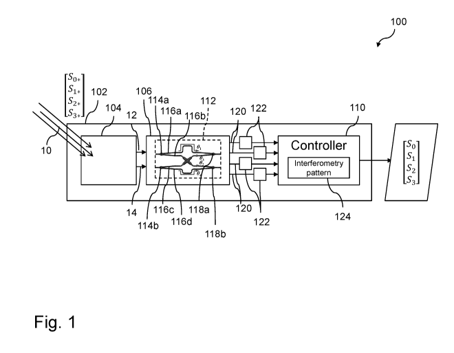
light beam can be performed by a controller. The computations may occur in
quasi-real time
as the intensities are measured in some embodiments whereas, in some other
embodiments, the measured intensities can be stored on a memory of the
controller for
subsequent computation. The controller can be provided as a combination of
hardware and
software components. The hardware components can be implemented in the form of
a
computing device 300, an example of which is described with reference to Fig.
3.
[00110] As depicted, the computing device 300 can have a processor 302, a
memory 304,
and I/O interface 306. Instructions 308 for determining the state of
polarization of the
incoming light beam can be stored on the memory 304 and accessible by the
processor 302.
For instance, the interferometry pattern, expressed in terms of matrix W, can
be stored on
the memory 304 and accessible by the processor 302.
[00111] The processor 302 can be, for example, a general-purpose
microprocessor or
microcontroller, a digital signal processing (DSP) processor, an integrated
circuit, a field
programmable gate array (FPGA), a reconfigurable processor, a programmable
read-only
memory (PROM), or any combination thereof.
[00112] The memory 304 can include a suitable combination of any type of
computer-
readable memory that is located either internally or externally such as, for
example, random-
access memory (RAM), read-only memory (ROM), compact disc read-only memory
(CDROM), electro-optical memory, magneto-optical memory, erasable programmable
read-
only memory (EPROM), and electrically-erasable programmable read-only memory
(EEPROM), Ferroelectric RAM (FRAM) or the like. The interferometry pattern can
be stored
on the memory 304 and accessible by the processor 302.
[00113] Each I/O interface 306 enables the computing device 300 to
interconnect with one
or more input devices, such as one or more optical detectors, a keyboard, a
mouse, a
pointer, or with one or more output devices such as a display, a remote
network and the like.
CA 03141895 2021-11-25
WO 2020/248046
PCT/CA2020/050786
22
[00114] Each I/O interface 306 enables the controller to communicate with
other
components, to exchange data with other components, to access and connect to
network
resources, to serve applications, and perform other computing applications by
connecting to
a network (or multiple networks) capable of carrying data including the
Internet, Ethernet,
plain old telephone service (POTS) line, public switch telephone network
(PSTN), integrated
services digital network (ISDN), digital subscriber line (DSL), coaxial cable,
fiber optics,
satellite, mobile, wireless (e.g. VVi-Fi, VViMAX), SS7 signaling network,
fixed line, local area
network, wide area network, and others, including any combination of these.
[00115] The computing device 300 described above are meant to be examples
only. Other
.. suitable embodiments of the controller can also be provided, as it will be
apparent to the
skilled reader.
[00116] Fig. 4 is a schematic view of a second example of a substrate-mounted
polarimeter
400. As depicted, the phase-retardant waveguides 416a, 416b, 416c and 416d
have
respective phase delays 01 , 02 , 03 , and 04 and the waveguide outputs 420
lead to
.. intensities /1 ,I , 13 , and /4 to be measured using corresponding detector
units. In this
example, the polarimeter 400 is a silicon photonic (SiP) four photodetectors
(PDs) division-
of-amplitude polarimeters (4PD-DOAPs) using a CMOS-compatible photonic
fabrication
process. The design of the polarimeter 400 targets to minimize the number of
optical
components.
[00117] As depicted, the polarimeter 400 has a substrate 402, a polarization
splitter 404 on
the substrate 402 and output waveguides 420 running on the substrate 402 and
outputting
first, second, third and fourth polarization components. In this example, the
substrate 402 is
designed for a standard 220-nm-thick silicon-on-insulator (S01) wafer.
[00118] The polarization splitter 404 receives an incoming light beam 10
having a given
.. state of polarization and polarization splits it into at least a first
light beam 12 having a first
polarization component and a second light beam 14 having a second polarization
component.
CA 03141895 2021-11-25
WO 2020/248046
PCT/CA2020/050786
23
[00119] In this example, the polarization splitter 404 is a four-way
polarization splitter, with
four splitter outputs. As shown, two of the splitter outputs propagate the
first and second light
beams 12 and 14 directly to respective output waveguides 420 without much
interfering. The
other two of the splitter outputs lead to the interferometry circuit 406 where
the first and
second light beams 12 and 14 are interfered with one another to form the third
and fourth
polarization components.
[00120] The interferometry circuit 406 has a first power splitter 414a which
power splits the
first light beam 12 into first and second phase-retardant waveguides 416a and
416b, and
also a second power splitter 414b which power splits the second light beam 14
into third and
fourth phase-retardant waveguides 416c and 416d. The interferometry circuit
406 also has a
first polarization coupler 418a polarization coupling the first and third
phase-retardant
waveguides 416a and 416c to one another forming the third polarization
component, and a
second first polarization coupler 418b polarization coupling the second and
fourth phase-
retardant waveguides 416b and 416d to one another forming the fourth
polarization
component.
[00121] As can be appreciated, the components of the polarimeter 400 are
optically
coupled to one another in the following way in this specific example. The
polarization splitter
has first and second splitter outputs outputting the first light beam and
third and fourth splitter
outputs outputting the second light beam. In this example, the first and third
splitter outputs
are optically coupled to corresponding output waveguides leading to respective
detector
units. The second splitter output leads to the first power splitter whereas
the fourth splitter
output leads to the second power splitter via corresponding waveguides. As
discussed
above, the first power splitter receives the first light beam from the second
splitter output and
outputs the first and second phase-retardant waveguides. The second power
splitter
receives the second light beam from the fourth splitter output and outputs the
third and fourth
phase-retardant waveguides. The first polarization coupler receives the first
and third phase-
retardant waveguides, thereby coupling the first and second light beams to one
another, and
leads to a corresponding output waveguide. Similarly, the second polarization
coupler
receives the second and fourth phase-retardant waveguides, thereby coupling
the first and
CA 03141895 2021-11-25
WO 2020/248046
PCT/CA2020/050786
24
second light beams to one another, in an asymmetric way, and leads to a
corresponding
output waveguide.
[00122] As discussed above, the third and fourth phase-retardant waveguides
416c and
416d are asymmetric with respect to the first and second phase-retardant
waveguides 416a
and 416b. More specifically, in this example, the first, second, third and
fourth phase-
retardant waveguides 416a, 416b, 416c and 416d have a respective one of first,
second,
third and fourth phase delays 01, 02, 03, and 04, with at least the first and
fourth phase delays
01 and 04 being different from one another.
[00123] As shown, the output waveguides 420 output the first, second, third
and fourth
polarization components towards a common portion 402a of the substrate 402,
where
intensities of the polarization components can be measured. As shown in this
example, the
intensity 11 of the first polarization component is indicative of an intensity
of the first light
beam 12, the intensity 12 of the second polarization component is indicative
of an intensity of
the second light beam 14, the intensity 13 denotes an intensity of the third
polarization
component, resulting from a linear combination of the first and second light
beams 12 and
14, and the intensity 14 denotes an intensity of the fourth polarization
component which
results from a different linear combination of the first and second light
beams 12 and 14.
[00124] The polarimeter 400 can produce a complete analysis matrix of an
optimally
conditioned polarimeter. Specifically, the polarimeter 400 is a division-of-
amplitude
polarimeter (DOAP) that splits the incoming light beam into several light
beams for fast,
simultaneous measurements. As the full reconstruction of the Stokes vector in
principle
requires only four intensity measurements, the interferometry circuit 406 of
the polarimeter
400 splits the incoming light beam 10 in a way that provide four polarization
components
from which the complete state of polarization (SoP) of the incoming light beam
can be
reconstructed.
[00125] As discussed above, the SoP is typically characterized by a 4 x 1
Stokes vector.
Therefore, complete reconstruction of the SoP requires a minimum of four
distinct
measurements, which can be realized by projecting the Stokes vector onto four
or more
analysis states determined by the Mueller matrix (analysis matrix) of the
polarimeter. In
CA 03141895 2021-11-25
WO 2020/248046
PCT/CA2020/050786
classical free-space optical systems, this operation can be achieved via
rotating polarizers or
via retarders in combination of a fixed polarizer. In a PIC, this can be
realized through
waveguide interferometers without mechanical moving parts. For instance, Figs.
5A-C show
PIC counterparts 500 of some free-space optical components 500' commonly used
in free-
5 .. space Stokes polarimeters. A SPS can decompose the two orthogonal E-field
components
(Ex and Ey), each coupling (ideally with equal power) into two single-mode
waveguides that
guide in opposite directions. As shown in Fig. 5A, the SPS functions as
combined
polarization beam splitter (PBS) and half-wave plate (HWP) in a conventional
free-space
optical system. An on-chip beam combiner (i.e., 3-dB Y-branch) coherently
combines Ex and
10 Ey (orthogonal in free space, but coupled to the same mode in two
waveguides), as shown
in Fig. 5B, outputting V2/2(Ex+Ey), which is equivalent to a 45 linear
polarizer. Fig. 5C
shows two phase-retardant waveguides, acting as a retarder, which thanks to
the different
lengths of the two waveguides, can introduce a phase difference between Ex and
Ey.
[00126] The polarimeter 400 transforms the Stokes vector into a series of
intensities that
15 can be detected by PDs. The analysis matrix W defines the
transformation:
[00127] I = W = S + n, (2)
[00128] where S = (SO,S1,S2,S3)T is the input Stokes vector, l=(11,12,...,IN)T
is an N-
dimensional vector representing the measured intensities, not to be confused
with the
identity matrix. The noise contribution of the PDs is n. The estimated Stokes
vector is
20 given by:
[00129] = Wt = W = S + Wt = n, (3)
[00130] where Wt denotes the generalized inverse of W, also known as the
synthesis
matrix. Here, only the case of N = 4 is considered, so that Wt = W-1-. The
error of the
estimated Stokes vector can be obtained by:
25 [00131] AS =
¨ S = W-1- = n. (4)
CA 03141895 2021-11-25
WO 2020/248046
PCT/CA2020/050786
26
[00132] Equation (4) shows that the estimation error is influenced by the
noise level and
the synthesis matrix. For noise n, with covariance matrix r, taking
expectations, one can
obtain:
[00133] Cov(g) = EtAS(AS)T = w-lr(w-1)T (5)
[00134] In the presence of additive white Gaussian noise (AWGN), and when the
noise at
each PD is zero mean and identically distributed with variance a, one can
have:
[00135] Cov(g) = a w-i (w-i)T (6)
[00136] The condition number K = IIWII 11W-111 is a figure of merit often used
to evaluate
polarimeter performance, where 11* II is the matrix form (taken as the L2 norm
throughout this
example). The detection SNR is maximized when the condition number is
minimized.
[00137] In the presence of shot noise (e.g., Poisson noise), assuming
independent noise in
each PD, the noise covariance matrix is diagonal with ith entry proportional
to the ith detected
signal power. For ilij, denoting the i,j element of matrix A, this means:
[00138] Fi j a (WS)11. (7)
[00139] Therefore, the variance of the Stokes estimate is SoP dependent for
Poisson
noise. As the signal power varies across PDs, the Poisson noise is not
identically distributed
(unlike the AWGN). For best performance, the polarimeter 400 would equalize
the noise
variances.
[00140] Matrix Q is thus defined by:
[00141] n
= E4n=1[W(i+11)ni Wn(i+1)' (8)
[00142] where ui = (Qi1, Qi2, Qi3)T, and P as the degree of polarization. As
the Poisson
variance depends on S, each component of g will have some maximum variance,
4/Lax, and
minimum variance, ylnin, associated with that component. The mean excursion
between
these extrema, Ay, is given by:
CA 03141895 2021-11-25
WO 2020/248046
PCT/CA2020/050786
27
[00143] Ay = En3=i(yimax _ yimin) = _2 = sop En3=1111111, (9)
3 3
[00144] The polarimeter 400 can equalize the noise for zero excursion, i.e.,
where
maximum noise variance yinax equal to minimum noise variance ylnin on each
Stokes vector
component. An optical structure is thus sought to minimize the condition
number K and the
variance difference Ay.
[00145] As such, the incoming light is split into four waveguides by the four-
way
polarization splitter. The optical waves propagating in the four waveguides
(e.g., A/2/2Eõ,
//2E, A/2/2Eõ, A//2E) carry the full information of SoP of the incoming light.
Two of the
optical paths are split into four paths by two 50:50 power splitters, and then
they separately
pass through unique Oi -phase-retard waveguides, and cross-coupled using 50:50
polarization couplers.
[00146] The first and second light beams 12 and 14 which pass through the
first and third
phase-retardant waveguides 416a and 416c are by construction coherent with
each other
and they combine to yield intensity /2. The first and second light beams 12
and 14 passing
through the second and fourth phase-retardant waveguides 416b and 416d are
also
coherent, yielding /3. This section of the polarimeter 400 is called a
crossing coherent
analyzer.
[00147] In this example, the remaining waveguides 426 do not pass through any
components, and yield intensities l and 12, respectively. A 3-dB optical
attenuator is added
before the PDs to distribute unpolarized light equally among the four outputs,
intensities
through Li. As discussed above, the asymmetricity between the first and second
phase-
retardant waveguides 416a and 416b and the third and fourth phase-retardant
waveguides
416c and 416d is provided by phase delays being different between the two
pairs of phase-
retardant waveguides. For instance, in some embodiments, the first, second,
third and fourth
phase-retardant waveguides 416a, 416b, 416c and 416d have a respective one of
first,
second, third and fourth phase delays 01, 02, 03, and 04. For instance, the
asymmetricity may
be obtained by ensuring that at least the first and fourth phase delays 01 and
04 are different
from one another, 01 # 04.
CA 03141895 2021-11-25
WO 2020/248046
PCT/CA2020/050786
28
[00148] The analysis matrix W1 of the polarimeter 400 is therefore:
/1 1 0 0
1 0 cos(01 ¨ 03) ¨ 03)
[00149] Wi oc = 1 0 cos(04 ¨ 02) sin(04 ¨ 02)
0 0
[00150] Fig. 6 shows the condition number K for the polarimeter 400 and is
plotted as a
function with (01 ¨ 03) and (04 ¨ 02). The minimum condition number Kinin can
be obtained
when:
[00151] (01 ¨ 03 + 04 ¨ 02) = (2m + 0.365)7, (11)
[00152] where m is any integer.
[00153] The polarimeter 400 cam be next improved by minimizing Ay, or
equivalently,
minimizing Ay = En3,11101. The variation of Ay with Oup for Eq. (11) is
depicted in Fig. 7. For
the m = 0 case, the minimum Ay is observed at (01 ¨ 03) = 0.18257 or 0.31757.
For this
design, (01 ¨ 03) has been selected to be 0.18257, see arrow in Fig. 7. The
experimental
characterization of the polarimeter 400 is discussed in the following
paragraphs. The
analysis matrix Wa is:
1 1 0 0
1 4 ¨.542
[00154] Wa 0 1 00.
08.84 0 0.542 (12)
[00155] The polarimeter 400 was fabricated using a CMOS-compatible process
with the
electron-beam lithography on an SOI platform, in which the thicknesses of the
silicon and
oxide layers are 220 nm and 2 pm, respectively. The scanning electron
microscope (SEM)
image of the polarimeter 400 is presented in Fig. 8A. The size of the strip
waveguides are
500 nm x 220 nm. The polarization splitter is formed using a 30 x 30 array of
cylindrical
holes fully etched through silicon with a period A of 695 nm and a hole
diameter D of 440 nm
(as shown in an inset of Fig. 8A). The numerical efficiency of the SPS is
given in Fig. 8B,
showing that its 3-dB bandwidth is 35 nm and that the centre wavelength is
1550 nm.
CA 03141895 2021-11-25
WO 2020/248046
PCT/CA2020/050786
29
[00156] An experiment setup to test the polarimeter 400 is shown in Fig. 9. A
linearly
polarized light beam is generated using a tunable laser. The SoP is controlled
by a polarizer
(650-2000 nm, Thorlabs), an HWP (1550 nm, Thorlabs), and a quarter-wave plate
(QWP,
1550 nm, Thorlabs). The orientation of the polarizer is fixed at 0 with
respect to the x-axis.
Rotating the HWP and QWP can allow generation of any SoPs. Two stepper motor
rotations
(K100R1/M, Thorlabs) are separately used to control the angles of the HWP and
QWP. The
four output waveguides of the polarimeter 400 are readout using off-chip
photodetectors
through optical fibers.
[00157] Through rotating the HWP and QWP, a series of SoPs can be generated
such that
the series of SoPs can spread widely over the surface of a Poincare sphere.
The polarimeter
400 was used to measure a plurality of SoPs of different incoming light beams.
The
measured results and the corresponding input SoPs are depicted in Fig. 10. A
satisfactory
agreement is observed between the input and measured SoPs. Because the
polarimeter 400
is unpackaged, the experimental set-up vibrations would cause near 0.8-dB of
intensity
measurement relative errors, which would bring near 0.114 of root-mean-square
(RMS) error
of the SoP measurements. Therefore, the RMS error of the Stokes vector
reconstruction is
very high and achieves 0.147 in this example. The RMS error can be
significantly reduced
after packaging or using integrated PDs on a chip.
[00158] The polarimeter 400 responds to a plurality of spectral components
(e.g.,
.. wavelengths). As such, the orientations of the HWP and QWP are fixed at 20
and 60 with
respect to the x-axis, respectively, and allow the tuning of the spectral
component of the
incoming light beam from 1540 nm to 1565 nm. The input SoPs as a function of
wavelengths
are shown in the dashed line of Fig. 11. The dots with error bar in the Fig.
11 are the
measured results of the polarimeter 400. The measured results can be observed
to agree
well with the corresponding input SoPs at other wavelengths.
[00159] The condition number of the polarimeter 400 described with reference
to Fig. 4 is
1.65, which is higher than the theoretical minimum value for a full-Stokes
polarimeter. The
noise variances of each Stokes element estimate are sensitive to the incoming
SoP in the
presence of signal-dependent Poisson shot noise.
CA 03141895 2021-11-25
WO 2020/248046
PCT/CA2020/050786
[00160] Fig. 12 is a schematic view of a third example of a substrate-mounted
polarimeter
1200. In this example, the polarimeter 1200 is another example of a silicon
photonic (SiP)
four photodetectors (PD) division-of-amplitude polarimeters (4PD-DOAPs) using
a CMOS-
compatible photonic fabrication process. The design of the polarimeter 1200
design makes
5 use of a slightly more complex circuit design to achieve an optimal frame
for measurements;
this measurement frame minimizes and equalizes estimation variances in the
presence of
both additive white Gaussian noise and signal dependent shot noise. Further
theoretical
examination reveals that within the optimal measurement frames for Stokes
polarimeters,
the DOAP with four PDs has the minimal equally weighted variance compared to
those with
10 a greater number of PDs. To the best of our knowledge, this is a
satisfactory demonstration
of a chip scale, solid-state full-Stokes polarimeter with an optimal
measurement frame
providing minimal and equalized noise variance on each Stokes channel.
[00161] As depicted, the polarimeter 1200 has a substrate 1202, a polarization
splitter
1204 on the substrate 1202 and output waveguides 1220 running on the substrate
1202 and
15 outputting first, second, third and fourth polarization components. The
substrate 1202 is
designed for a standard 220-nm-thick silicon-on-insulator (S01) wafer.
[00162] The polarization splitter 1204 receives an incoming light beam 10
having a given
state of polarization and polarization splits it into at least first and
second light beams 12 and
14.
20 [00163] In this example, the polarization splitter 1204 is a two-way
polarization splitter, with
two splitter outputs. As shown, a first one of the splitter outputs propagates
the first light
beam 12 towards a first asymmetric splitter 1228a whereas a second one of the
splitter
output propagates the second light beam 14 towards a second asymmetric
splitter 1228b. As
one branch of the first and second asymmetric splitters 1128a and 1228b leads
to a first
25 interferometry circuit 1206a, the other branch thereof leads to a second
interferometry circuit
1206b. As shown, the first and second asymmetric splitters 1128a and 1228b
couple
towards the second interferometry circuit 1206b with a coupling factor PR and
couple
towards the first interferometry circuit 1206a with a complementary coupling
factor of
PR' =1¨ PR.
CA 03141895 2021-11-25
WO 2020/248046
PCT/CA2020/050786
31
[00164] Each of the first and second interferometry circuits 1206a and 1206b
has a similar
construction than the interferometry circuit 406 of the polarimeter 400 shown
in Fig. 4.
Referring back to Fig. 12, the first asymmetric power splitter 1228a power
splits the first light
beam 12 towards the first power splitter of the first interferometry circuit
and a first power
splitter of the second interferometry circuit. Similarly, the second
asymmetric power splitter
1228b power splits the second light beam 14 towards the second power splitter
of the first
interferometry circuit and the second power splitter of the second
interferometry circuit.
[00165] As can be appreciated, the components of the polarimeter 1200 are
optically
coupled to one another in the following way in this specific example. The
polarization splitter
has first and second splitter outputs outputting the first and second light
beams, respectively.
The first and second light beams are both split in an asymmetric fashion
towards a
respective one of the first and second interferometry circuits via the first
and second
asymmetric power splitters. As such, the first light beam is propagated
towards the first
power splitter of the first interferometry circuit and towards the first power
splitter of the
second interferometry circuit. Similarly, the second light beam is propagated
towards the
second power splitter of the first interferometry circuit and towards the
second power splitter
of the second interferometry circuit. As such, the first polarization coupler
of the first
interferometry circuit leads to the first polarization component, the second
polarization
coupler of the first interferometry circuit leads to the second polarization
component, the first
polarization coupler of the second interferometry circuit leads to the third
polarization
component, and the second polarization coupler of the second interferometry
circuit leads to
the fourth polarization component.
[00166] As shown, the first, second, third and fourth phase-retardant
waveguides 1216a,
1216b, 1216c and 1216d of the first interferometry circuit 1206a have a
respective one of
first, second, third and fourth phase delays OL O, O, and O, whereas the
first, second, third
and fourth phase-retardant waveguides 1216a, 1216b, 1216c and 1216d of the
second
interferometry circuit 1206b have a respective one of said fourth, third,
second and first
phase delays 0, O, O, and OL with at least said first and fourth phase delays
0;_ and Od'i,
being different from one another.
CA 03141895 2021-11-25
WO 2020/248046
PCT/CA2020/050786
32
[00167] As such, the polarimeter 1200 has two interferometry circuits 1206a
and 1206b
each having a respective crossing coherent analyzer and two asymmetric power
splitters
(APS) 1228a and 1228b. The APS 1228a and 1228b are located between the
polarization
splitter 1204 and the interferometry circuits 1206a and 1206b. Fig. 13 shows
an example of
an asymmetric power splitter. For APS, the values of the weaker and the
relatively longer
output power ratio are denoted by PR and (1-PR), respectively. In this
example, the length
(L) and width (2w) of the splitting region of APS are equal to 2.32 pm and 1.4
pm,
respectively. By controlling the asymmetry of APS, the output power ratio PR
can be
controlled. Besides, a 2-ports SPS is designed to replace the 4-ports SPS. To
increase the
efficiency of the 2-ports SPS, two distributed Bragg reflection (DBR) gratings
are added at
two idle ports of the SPS. DBR gratings can reflect the lights back to the
desired
waveguides.
[00168] In this example, the polarimeter 1200 has an interferometry pattern
represented by
a synthesis matrix W2, in which the state of polarization S of the incoming
light beam is
determinable using the equation S = W2 = I, where S is a vector denoting said
state of
polarization (So, Sl, S2, 53)T of the incoming light beam, and I is a vector
denoting intensities
(ILJ /,/:i)-r of the polarization components. The synthesis matrix W2 is given
by a matrix
equivalent to the following matrix:
hT-1 2-rrcos(0¨O) ¨2-rrsin(0¨O)\
T+1 T+1 T+1
1 T¨I- 2-rrcos(01¨O) 2-rrsin(01¨O)
T+1 T+1 T+1
[00169] W2 = (13)
1 -r 1¨T 2rcos(0 -r 1¨OD ¨2rsin(01¨O)
T+1 T+1 r+1
\ 1 I--T 2-rrcos(0¨O) 2-rrsin(0¨O)
\ T+1 T+1 T+1
[00170] where T denotes a ratio of the coupling coefficients represented by
PR/(1¨ PR).
There are only two analysis matrices (within arbitrary row permutations) which
have the
properties of K = 11 and Ay = 0. The two analysis matrices Wb and Wb, have the
following
formulas:
CA 03141895 2021-11-25
WO 2020/248046
PCT/CA2020/050786
33
4 - 4 -4\
3 3 3
1 1 1
1 -
3 3
[00171] Wb oc A and (14)
.., ,
¨
1 1 1
/1 -4 4 -4\
1 1 1
1 - -
3 3 A/7
[00172] Wb OC A , (15)
..,
¨
1 1 1
\ 7 7 7
[00173] where A is a positive value (0 <A 1/2), and here A=1/4. Comparing Eqs.
(13)
with (14) and (15), one can obtain that when T = 2 ¨a the condition number of
the
polarimeter would have the potential to achieve optical performance. When T =
2 ¨ the
condition number as a function with
OD and (K- OD is presented in Fig. 14, which
shows that when ¨ = 2nrc + 7/4 and WI,-
= 2nrc + 37/4 (where n is an integer),
the optical condition number (ATh can be obtained. The analysis Wb can be
achieved when
(O¨ = 37/ 4 and WI,- = 7/4.
[00174] The structure of ¨ = 37/4, WI,- = 7/4,
and T = 2 ¨ was chosen to
be fabricated and experimentally demonstrated. In this example, the
polarimeter 1200 has a
footprint of 350 x 460 pm2. The DBR can consist of eight alternating layers of
silicon and
silicon dioxide in some embodiments. The width of silicon layer, and the
lattice period are
160 nm, and 360 nm, respectively. The polarimeter 1200 was used to measure a
series of
SoPs, and the corresponding results are depicted in Fig. 15. The measured
results agree
well with the input SoPs. Its RMS error is near 0.081 which is 44% lower than
that of the
polarimeter 1200 under the same 0.8-dB of intensity measurement relative
errors caused by
the vibrations of the experimental set-up.
[00175] The polarimeter 1200 can be regarded as a projector that projects the
input Stokes
vector onto an intensity vector of measurement. For simplicity, one normalizes
the analysis
matrix W so that W = Wi22 + Wi23 + Wi24 = 1, where i means the ith row of the
matrix.
CA 03141895 2021-11-25
WO 2020/248046
PCT/CA2020/050786
34
Therefore, the endpoints of the reduced vectors wi1 = (wi2,wi3,wi4) are
located on the
surface of a Poincare sphere. The measurement frame (i.e., the set of vectors
twO) can be
described by a polyhedron whose vertexes are defined by the endpoints of the
reduced
vectors wi. It has been demonstrated that the Platonic polyhedron can achieve
the minimum
condition number. The polarimeter 1200 whose measurement frame is an irregular
tetrahedron does not have the minimum condition number. The regular
tetrahedron is a
spherical 2-design with N=4, which has been proven to not be able to realize
noise variance
equalization except for two particular orientations in the presence of Poisson
noise.
However, this limitation can be broken via the regular octahedron, which is
the simplest
spherical 3-design. The regular octahedron is one example: when rotated to
another
orientation, it remains such a property.
[00176] A number of polyhedrons can realize a minimal and equalized Poisson
noise
variance, but can suffer from different additive Gaussian noise. Here, one
examines the
impact of the detection number N on the total variance of the four Stokes
channels (termed
as equally weighted variance, EVVV). Consider the cases of Platonic
polyhedrons. The
optical power received by each PD is proportional to So/N (i.e., the DOAP, and
the division of
time polarimeter, DOTP which used in the scenario of "photon-starved"). In
these cases, the
analysis matrix W has the following properties:
[00177] Vi(i = 1,2, =!, (16)
[00178] and
3 0 0 0\
[00179] = 0 1 0 )'
0 0 (17)
3N 0 1 0
0 00 1
[00180] where WT is the transpose of W. For AWGN, EVVVadd is given by:
[00181] EWI/cidd = 0-7,2 = Tr[(WTW) 1], (18)
CA 03141895 2021-11-25
WO 2020/248046
PCT/CA2020/050786
[00182] where a is the variance of the additive noise, and Tr(*) means the sum
of the
elements on the main diagonal (the diagonal from the upper left to the lower
right) of *.
Based on Eqs. (15) and (16), one can obtain that:
[00183] EWVadd = 10N0-7,2. (19)
5 [00184] For Poisson noise, EVVVpo, has the following expression:
[00185] EWVpoi = W11 = So = Tr[(WTW)]. (20)
[00186] Based on Eqs. (16), (17) and (20), one can obtain that:
[00187] EWVpoi = 10S0. (21)
[00188] From Eq. (19), one can know that in the presence of the additive
noise, EWVadd
10 increases with N. Therefore, the regular tetrahedrons in the two
specific orientations are the
best architectures. On the other hand, Eq. (20) indicates that the EWVpoi is
independent of
the numbers of PDs. Overall, 4PD-DOAP not only has a relatively low cost in
signal
processing, but also is less influenced by noise in the reconstructions of
SoP. Notice that the
conclusion may be opposite for a DOTP, where no power splitting is required
and SoP is
15 detected at a relatively low speed. In this case, people usually take
more measurements to
suppress noise.
[00189] The above paragraphs discuss a demonstration of a chip scale, solid-
state full-
Stokes polarimeter with an optical frame in the presence of both Gaussian and
Poisson
noises. Two ultra-compact full-Stokes polarimeters 400 and 1200 have a minimum
number
20 of detector units and a CMOS-compatible fabrication process. The designs
of these
polarimeters were optimized taken into consideration both the condition number
and
estimated variance. A polarimeter architecture for an optical 4PD-DOAP
analysis matrix (Wb
and Wb,) with the minimum condition number (K='A and Poisson shot noise
equalization
(Ay = 0) has been achieved in a PIC. Excellent agreement has been shown
between the
25 measured results using the polarimeters 400 and 1200 and a bench-top
commercial
instrument. It was shown that, within the optical frames of Stokes
polarimeters, increasing
CA 03141895 2021-11-25
WO 2020/248046
PCT/CA2020/050786
36
the number of detections beyond four through power division causes a higher
additive
Gaussian noise while the Poisson shot noise is not affected. Therefore, 4PD-
DOAP offers a
theoretically optical DOAP design. The polarimeters 400 and 1200 can also be
extended to
other materials platforms, such as silicon nitride, and germanium for the
visible and mid-
infrared ranges. Furthermore, these compact polarimeters 400 and 1200 can be
readily
integrated with other silicon photonics devices such as spectrometers so that
a
comprehensive optical vector analysis can be achieved on a single chip for
even broader
applications.
[00190] As mentioned above, the polarization splitter can be provided in the
form of an
.. assembly comprising an edge coupler and a polarization splitter rotator.
Fig. 16 shows a top
plan view of a third example of a polarimeter 1600 comprising such a
polarization splitter. As
depicted, the polarimeter 1600 has a substrate with a top surface and at least
a lateral
surface or edge. An interferometry circuit such as the ones described above is
also on the
substrate.
[00191] As illustrated, the polarization splitter has an edge coupler disposed
on the lateral
surface or edge of the substrate. In this way, a light beam incoming in a
parallel manner to
the top surface of the substrate will be injected in waveguide(s) of the
polarimeter 1600 via
the edge coupler. To split the polarization of the incoming light beam, the
polarization splitter
has a polarization splitter rotator which polarization splits the incoming
light beam into the
first and second light beams. In some embodiments, the polarization splitter
rotator splits the
two orthogonal linear polarization components (i.e., TE and TM modes) of the
incoming light
beam into two waveguides directed respectively to the first and second power
splitters of the
interferometry circuit. The TM mode of the incoming light beam is thereby
rotated into the TE
mode.
[00192] The polarimeter has detection units provided in the form of spaced-
apart
photodetectors such as photodiodes which are optically coupled to the
interferometry circuit
to receive the first, second, third and fourth polarization components. As
shown, the
photodiodes have sensors receiving the polarization components and generating
corresponding signals which can be pickup at conducting pads electrically
coupled to the
sensors. In this embodiment, the detector units can be communicatively coupled
to the
CA 03141895 2021-11-25
WO 2020/248046
PCT/CA2020/050786
37
controller via a wired connection. In some other embodiments, the signals can
also be
communicated in a wireless manner.
[00193] In some embodiments, it might be preferable to increase the spectral
band within
which the polarization components can satisfactorily propagate. Fig. 17 shows
a fourth
example of a polarimeter 1700. Although similar to the polarimeter 1200, the
phase-retardant
waveguides of the polarimeter 1700 are wavelength independent. For the first
and second
asymmetric power splitters, the output power ratio of the weaker paths and the
relatively
stronger paths are denoted by PR and (1 - PR), respectively. The phase shift
in the two
paths as Ow and cps, respectively. The crossed coherent analyzer consists of
phase-retardant
.. waveguides provided in the form of subwavelength gratings (SWGs), examples
of which are
shown in Fig. 18. Fig. 19 shows the phase difference between the two SWGs of
Fig. 18
across a given spectral band. The phase shifts of the four SWG waveguides are
represented
as el, e2, e3, and al, respectively.
[00194] As discussed above, when (e1 - e3) - (Ow - Os) = 2nn- n-A and (e4 -
e2) + (Ow -
Os) = 2nn- 3n-A, or (e1 - e3) - (ow -Os) = 2nn- 37-7-4 and (e4 - e2) + (ow
-0) = 2nn- n-A
(where n is an integer), one can obtain an optimal polarimeter in the presence
of Gaussian
and Poisson shot noise. Here, the parameters of (e1 - e3) - (Ow - Os) = TTAI.
and (e4 - e2) +
(ow - os) = 3n-A are selected as an example to design a broadband optimal
polarimeter.
The optimal polarimeter also requires PR/ (1 - PR) = 2
0.2679 in this specific
example.
[00195] Fig. 20 shows the PR/ (1 - PR) and (Ow - Os) of the asymmetric power
splitter
as a function of wavelength. The variation of the PR/(1 - PR) is less than
0.05 over a
wavelength range of 1.45 pm to 1.65 pm. The mean and variation of the (Ow -
Os) are
12.81 and 8.28 , respectively. To compensate for (Ow - OA the mean and
variation of
(e1 - e3) should be 57.81 and 8.28 , respectively. An asymmetric SWG PS with
W1 = 1.5
pm, W3 = 1.3 pm, LT1 = LT3 = 5.4 pm, and Np1 = Np3 = 11 was selected to
realize such a
phase shift. As shown in Fig. 21, the variation of (e1 - e3) - (Ow - os)
decreases to 4
after compensation. Similarly, the mean and variation of (e4 - e2) should be
122.19 and
-8.28 , respectively. To achieve a variation of -8.28 , we cascaded two SWG
PSs
.. together as shown in Fig. 1700. The structural parameters of the two SWG
PSs were: W21 =
CA 03141895 2021-11-25
WO 2020/248046
PCT/CA2020/050786
38
1.3 pm, W41 = 1.5 pm, LT21 = LT41 = 3 pm, Np21 = Np41 = 108, and W22 = 1.5 pm,
W42 = 1.3
pm, LT22 = LT42 = 6.8 pm, Np22 = Np42 = 0. The (e4 -e2)+(ow-os) as a function
of the
wavelength is presented in Fig. 21.
[00196] Fig. 22 shows a fifth example of a polarimeter 2200, in accordance
with another
embodiment. As depicted, the polarimeter 2200 has a polarization splitter and
an
interferometry circuit which leads to output waveguides each carrying a
respective one of
first, second, third and fourth polarization components. As can be
appreciated, the
polarization splitter and the interferometry circuit of this embodiment are
similar to those
described with reference to the polarimeter 400 of Fig. 4.
[00197] As will be described, the polarimeter 2200 is suited for determining a
spectrally-
varying state of polarization of the incoming light beam. More specifically,
each of the
detector units has an optical spectrum analyzer which can measure intensities
at a plurality
of spectral components for the corresponding polarization components. Each
optical
spectrum analyzer has a tunable filter which is tunable to direct a given
spectral component
towards a corresponding photodiode which measures the intensity at the
selected spectral
component. By sweeping the tunable filter across a given spectral band,
intensity
measurements at a plurality of spectral components can be measured
successively. The
construction of the optical spectrum analyzer can differ from one embodiment
to another.
However, in this specific embodiment, each optical spectrum analyzer or
spectrometer is
provided in the form of a microring resonator which can act as a filter to
pick up a given
spectral component from an incoming polarization component. As shown, each
microring
resonator can be tuned by modifying its temperature using heating elements. By
contracting
or expanding the microring, the coupling condition will vary thereby acting as
a tunable filter.
The four output spectra, I1(A) to I4(A), are eventually used to reconstruct
wavelength-
dependent Stokes parameters through linear matrix operations, as discussed
above.
[00198] The polarimeter 2200 is thereby an example of a spectroscopic
polarimeter which
can be used in combination with a broadband source or optical frequency comb
to measure
matter-light interactions in both the spectral and polarization domains. As
shown, the optical
spectrum analyzers receive the polarization components from the interferometry
circuit, and
redirect them towards a plurality of spectrally spaced-apart channels. Each of
the spectrally
CA 03141895 2021-11-25
WO 2020/248046
PCT/CA2020/050786
39
spaced-apart channels has a given spectral component or wavelength. As shown
in this
example, the optical spectrum analyzers have microring resonator(s)
redirecting the
spectrally-spaced channels into a plurality of optical detectors, e.g.,
photodiodes.
Accordingly, the optical detectors are optically coupled at least to the drop
ports of the
microring resonators and measure corresponding intensity values from the
plurality of
spectrally spaced-apart channels. The controller, which is remote from the
substrate in this
example, can be configured to determine a spectrally-resolved state of
polarization of the
incoming light beam based on the measured intensity values and on the
interferometry
pattern of the interferometry circuit.
[00199] In some embodiment, the polarimeter 2200 can be designed based on a
standard
220-nm-thick silicon-on-insulator (S01) wafer with a 2 pm buried oxide layer
and 3 pm oxide
cladding. The polarization splitter can be provided in the form of a surface
polarization
splitter (SPS) used to project an arbitrary state of polarization into two
orthogonal linearly
polarized components (E, and Ey) and couple them into different waveguides.
The
interferometry circuit then converts the two orthogonal E-field components
into four
polarization components. The spectrum of each polarization component is
measured using
an optical spectrum analyzer consisting of a thermally tunable silicon
dualmicroring
resonator and a Ge-PD. The four spectral measurements thereby capture the full
information
of wavelength-dependent polarization, from which the Stokes spectra of the
input light can
eventually be retrieved via a matrix operation. As depicted in Fig. 22, the
black arrows point
to the propagating direction of light.
[00200] The SPS makes use of a nanoantenna structure, consisting of a 2D array
of sub-
wavelength cylindrical holes on a Si substrate in this example. The
nanoantenna is designed
so that both orthogonal linearly polarized components of the light, either
from an optical fiber
or free space, are coupled into the fundamental TE mode of the planar
waveguides.
Simultaneously, the SPS decomposes each orthogonal component equally into two
splitter
outputs in opposite directions as shown in Fig. 22.
[00201] The interferometry circuit consists of a 3-dB broadband directional
coupler (BDC),
three Y-junctions for 3-dB power splitting/combination, and a few delay lines.
Taking the
outputs of the SPS, the PA projects the Stokes vector of the incoming light
into four intensity
CA 03141895 2021-11-25
WO 2020/248046 PCT/CA2020/050786
channels through interference operation: /1 and /4 from direct detection of
¨Er and
2
respectively; /2 from the interference between ¨Ex and lEy ; /3 from the
2 2 2
interference betweenE x and ¨1+/E. Here, the incoming polarization is denoted
by
4 4
a wavelength (A) dependent Stokes vector: S (A) = (So (A), S I (A), S2 (A), S3
(A))7-, where
5 (Y)7- means the transpose of the matrix (Y). Defining a wavelength-
dependent intensity vector:
I (A) = (11 (A), 12 (A), 13 (A), 14 (A))7-, the relationship between I (A) and
S (A) can be given by:
S (X) oc Ms (X) I (X) (22)
where Ms (A) is the synthesis matrix of the PA. The BDC used in the proposed
spectropolarimeter design has a wide bandwidth in excess of 100 nm. Thus the
synthesis
10 matrix Ms (A) can be practically wavelength insensitive in the spectral
range considered in
this example and can be written by the following expression,
( 1 0 0
1 0 0 ¨1
Ms (2) = 2
¨1 0 1 ¨1
¨1 [00202] 2 0 ¨1
(23)
[00203] Following the PA circuit, four silicon dual-microring resonator
spectrometers (Si-
DMRSs) are used to measure the spectra of the intensity channels. Each Si-DM
RS consists
15 of an SDMR and a Ge-PD. The MRs in the SDMR have slightly different
FSRs. Due to the
Vernier effect, the cascaded architecture can achieve a largely extended FSR
without using
ultra-small MRs that are challenging for fabrication on a wafer scale. The
extended FSR of
the SDMR is given by,
FS FSR1=FSR2 Az Az
R , ¨ ,
IFSRi¨FSR21 27-tring2 ¨R2ngi 27z-ngi ¨R2I
[00204] (24)
CA 03141895 2021-11-25
WO 2020/248046
PCT/CA2020/050786
41
[00205] where FSR1(2), Di(2), and no(2) are the FSR, diameter, and group index
of the single
MRs, respectively; the subscript 1(2) indicates the first (second) MR. It is
noted that no ng2
when the diameters of the two rings are very close. According to Eq. 6.3, the
extended FSR
of the SDMR can be increased by decreasing the difference of the diameters. A
metal heater
is used on the top of each MR to individually vary their temperatures. Tuning
the heating
powers (HPs) applied to the MRs, the wavelength of each intensity channel, I
(A), can be
continuously swept and then detected by a Ge-PD. As shown in this example, the
fabricated
silicon photonic chip sits in the centre of a printed circuit board (PCB). Its
footprint can be of
about ¨ 1 x 0.6 mm2 or smaller. In some embodiments, the chip includes 16
electric I/O
ports.
[00206] Before experimenting with the full-Stokes spectrometer, a single Si-
DMRS
integrated with a Ge-PD on the same chip was first characterized. In this
specific example,
the diameters of two MRs can be 26 pm for the bigger microring and 22 pm for
the smaller
microring, respectively. A Ge-PD design without doped Ge or Ge-metal contacts
was
adopted in the polarimeter 2200. Because the germanium lattice is not
disturbed by dopants
or metal contacts in this example, it can allow for better performance in
background loss,
bandwidth, and dark current. The Ge-PD was measured to have a responsivity of
1.12 A/W
and dark current of ¨15 nA at -4 V reverse bias, at 1550 nm wavelength.
[00207] Fig. 23 shows a relation between resonance wavelength and heating
power on the
heaters of larger microring (red dot) and smaller microring (blue square). The
centre
wavelength as a function of HPs applied to the larger and smaller microrings
were calibrated
for each channel using a tunable laser. The calibration result is shown in
Fig. 23. The tuning
efficiency is ¨10 mW/nm and ¨11 mW/nm for the larger and smaller microrings,
respectively. Thanks to the Vernier effect, the maximum HPs required to cover
the entire
extended FSR for the larger and smaller microrings are only ¨70 mW and ¨100
mW,
respectively. To verify the stability of the polarimeter 2200, several
measurements were
performed within a week using the same HP calibration. The measurement results
show
excellent agreement over six day, indicating a very stable operation of the
polarimeter 2200.
[00208] As shown in Figs. 24 and 25, the transmission spectrum of the drop
port of the
fabricated SDMR can have a resonance wavelength near 1561 nm. As best seen in
Fig. 24,
CA 03141895 2021-11-25
WO 2020/248046
PCT/CA2020/050786
42
the 20-dB linewidth can be near 0.9 nm in this example. A bimodal filter shape
was designed
for a sharper roll-off on its edges to increase the signal-to-noise ratio
(SNR). An extended
FSR of 50 nm is measured such as shown in Fig. 25.
[00209] In an example experiment, the polarimeter 2200 was used to
characterize the
polarization of a chiral material, i.e., a cholesteric liquid crystal (CLC)
slab. It consists of
chiral molecules with a mechanical twisting power, which imposes a macroscopic
helicoidal
self-organization. As a result, the local average orientation of long
molecular axis is
periodically rotating from layer to layer, forming a natural molecular helix
(i.e. "structural
chirality"). With a proper choice of the molecular mixture parameters, the CLC
slab acts like
a spectral resonant filter (e.g., Rocking filter) in a desired spectral range,
which only left-
handed (or right-handed) circular polarization can pass through. The most
complex behavior
occurs at the edges of the resonant wavelength range where polarization
sensitive reflection
and strong polarization rotations (along with strong dispersion) are present.
To demonstrate
efficacy of the proposed spectropolarimeter, a CLC sample with an edge of the
resonant
range near 1550 nm was fabricated.
[00210] All the four Si-DMRSs were calibrated following the same procedure
described in
the previous section. The wavelength dependent synthesis matrix of the PA,
M(A), was also
calibrated using four known independent polarization states. Results show the
Stokes
spectra after the CLC sample with a linear polarization input (S1 = 1).
Excellent agreement is
observed in the measurement results between the polarimeter 2200 and a
commercial
bench-top instrument. The resonant range of the fabricated CLC material was
found to be
below 1.52 pm. In the resonant range, only left-handed circular polarization
can pass
through the CLC; S3 evolves towards -1, while Si and S2 approaches zero as
wavelength
decreases. While in the non-resonant range (beyond 1.58 pm), the CLC material
does not
change the input polarization state. Therefore, Si was found to increase
gradually from 0
towards 1 with the wavelength, while S3 increases from -1 to 0 in the non-
resonant range.
[00211] In spite of compactness, the polarimeter 2200 remains a high
performance with a
high resolution (1 nm) and broad bandwidth (50 nm) of Stokes spectrum, which,
however,
has still not reached its limits. For example, according to Eq. 24, a
bandwidth of 100 nm can
be obtained by increasing the diameter of the larger microring to 24 pm.
Besides, the
CA 03141895 2021-11-25
WO 2020/248046
PCT/CA2020/050786
43
spectral resolution of the polarimeter 2200 can be further proved by another
order of
magnitude (to 0.1 nm) by decreasing the cross-coupling coefficient between the
two
microrings without introducing significant loss.
[00212] Due to the employment of the Si-DMRS, the energy consumption is
significantly
reduced. The polarimeter 2200 was found to dissipate near 3.6 J of energy to
complete one
measurement of the Stokes spectra. Compared to traditional equipment, this
value can
represent a few orders of magnitude improvement. Moreover, the energy
consumption of the
polarimeter 2200 can be significantly improved by adding thermal isolation
trenches near the
MRs (> 10 times), and by increasing the sweeping frequency of the HP (> 100
times). Due to
the limitation of the experimental set-up, the sweeping frequency was only 5
Hz. While the
thermal response time of the microring is lower than 4 ps, indicating that a
sweeping
frequency of 250 kHz is possible. Assuming a higher sweeping frequency of 5
kHz for a
larger number of spectral sweeping steps of 1,000 (versus 50 in our current
experiment), the
total energy consumption of the polarimeter 2200 is estimated to be only ¨72
mJ. In this
case, one measurement of Stokes spectra can be accomplished within 0.2 s.
[00213] Achieving an integrated polarimeter, such as the polarimeter 2200, on
a silicon
photonic chip paves the way towards fast, affordable full-Stokes spectroscopy.
To decrease
the cost and size of the device, traditional solutions come with a reduced
number of
spectroscopic components, and consequently, compromised measurement speed and
Stokes spectral resolution. By contrast, the polarimeter 2200 in this example
allows for
simultaneous achievement of a high speed and a high resolution as all the Si-
DMRSs can be
integrated on a single chip with little increase in footprint and cost. The
polarimeter 2200 is
fabricated using industry-standard silicon photonics foundry processes,
indicating an easier
path towards mass production using established large-wafer manufacturing
facilities. The
operating frequency range can be readily extended to the visible and mid-
infrared regions by
using other CMOS-compatible materials (e.g., SiN and Ge) but the same
architecture.
Leveraging the economies of scale and advantages of silicon PICs integration,
the
polarimeter 2200 has a vast potential for application in the fields of
Internet of Things,
pharmaceutical analysis, astronomy, and so on.
CA 03141895 2021-11-25
WO 2020/248046
PCT/CA2020/050786
44
[00214] The device was fabricated using a commercial CMOS-compatible SOI
process
with 193 nm deep-UV lithography at IME (now AMF Pte Ltd), Singapore. The
devices were
subsequently packaged at a laboratory. The electrical connections were
realized using
Westbond's 7400A Wire Bonder. The plastic cover shell was fabricated using a
3D printer
(Ultimaker S5).
[00215] Sample Fabrication. The CLC material used was a mixture of
commercially
available Nematic Liquid Crystal (NLC) 20608 (Qingdao Chemicals) and the
chiral molecule
CB15 (Merck). Their ratio (75:25 wt % ratio) was adjusted, so that a CLC with
selective
reflection band in the near IR region could be obtained. The CLC mixture was
heated above
the clearing point (isotropic phase transition) and filled into the LC cell of
9.6 pm thickness
by capillary method and then was slowly cooled down to the room temperature.
The cell
consists of two indium tin oxide /ITO/ coated transparent glass substrates,
which are coated
with alignment layers that align CLC molecules parallel to the surface of the
substrates.
[00216] The calibration of the HPs described in the main text was performed
using a
tunable laser source (Agilent 81600B) with optical power around 3 dBm. The
photocurrents
from Ge-PD were read by a Keithley 2612B sourcemeter. The HPs of the heaters
were
driven using a Keysight E3631A power supply. The light from a high-power wide-
band
Erbium ASE source (INO) was used to characterize the Si-DMRS. A commercial
optical
spectrum analyzer (OSA, Yokogawa AQ6370D) was used to measure its spectrum.
The
synthesis matrix of the pro- posed spectropolarimeter was calibrated by a
polarizer (650-
2000 nm, Thorlabs), an HWP (1550 nm, Thorlabs), and a quarter-wave plate (QWP,
1550
nm, Thorlabs). Two stepper motor rotators (K10CR1/M, Thorlabs) were used to
control
separately the angles of the HWP and QWP.
[00217] Fig. 26 shows an example of a polarization imager 2600, in accordance
with an
embodiment. As shown, the polarization imager has a substrate, a plurality of
the
polarization splitters spaced-apart from one another on the substrate for
receiving
corresponding spaced-apart incoming light beams. The polarization splitters
polarization split
each of the incoming light beams into at least a first light beam having a
first polarization
component and a second light beam having a second polarization component. The
polarization imager has interferometry circuits optically coupled to one or
more of the
CA 03141895 2021-11-25
WO 2020/248046
PCT/CA2020/050786
polarization splitters. The interferometry circuits make an interference
between the first and
second light beams to form at least third and fourth polarization components,
such as
discussed above with the other polarimeter examples. More specifically, in
this example, the
polarization imager has output waveguides which output the polarization
components of the
5 incoming light beams, wherein intensities of said polarization components
and interferometry
patterns of the interferometry circuits are indicative of the states of
polarization of said
incoming light beams. As the polarization components fully defining a state of
polarization of
each of the spaced-apart incoming light beams, a polarization image can be
generated on
the basis of the intensities of the polarization components.
10 [00218] In this specific example, the polarization imager has a number
of polarimeters
disposed in an array on the substrate for receiving the incoming light beams.
In some
embodiments, the polarimeters are similar to the ones described above. As
shown, the
polarization imager has a plurality of polarization splitters and a plurality
of interferometry
circuits optically coupled to one another on the substrate. In some
embodiments, there can
15 be an equivalent or lesser number of interferometry circuits than of
polarization splitters. In
the latter case, optical switch(es) may be used to sequentially couple the
polarization
splitters and the interferometry circuits to one another. As best shown in
Fig. 26A, the
polarization splitters can be two-way polarization splitters in this
embodiment. Fig. 26B
further shows that the polarization splitters are surface polarization
splitters having an array
20 of cylindrical holes fully etched through silicon. In some embodiments,
the interferometry
circuits are similar to the ones described above. As shown, the polarization
imager has a
plurality of detector units coupled to output waveguides incoming from the
interferometry
circuits for measuring corresponding intensity values from the interferometry
circuits. In any
case, the polarization imager has a controller determining a state of
polarization associated
25 with each of the polarization splitters of the array based on the
measured intensity values,
and outputting a polarization image based on the determined states of
polarization of the
incoming light beams.
[00219] In this example, the polarization imager can have a compact footprint
and thereby
achieve a relatively large fill factor. As mentioned, a number of the
polarization splitters can
30 .. share one set of optical interferometry circuit and integrated PDs
through on-chip optical
CA 03141895 2021-11-25
WO 2020/248046
PCT/CA2020/050786
46
switches so that the polarization state received by each SPS can be analyzed
in a time
series. Each polarization splitter PS connects with bus waveguides through two
on-chip
optical switches. When the on-chip optical switches of a polarization splitter
are turned on,
two orthogonal electric field components of the incoming light can propagate
from the
corresponding polarization splitter to two bus waveguides, respectively. Then,
two
orthogonal electric field components of the incoming light are injected into
the optical
interferometry circuit. Measuring the optical intensities of the optical
interferometry circuit
output ports, the polarization state of the incoming light of the
corresponding polarization
splitter can be reconstructed. In this example, if these polarization
splitters are turned on one
by one, a polarization image can be obtained.
[00220] In this example, spectroscopic polarimetry is discussed. For instance,
principles for
channelled spectrum modulator (CSM), which can modulate the Stokes parameters
into the
channelled spectrum, and on-chip optical spectrum analyzer (OSA) for obtaining
the
channelled spectrum, are provided.
[00221] Fig. 27 shows another example of a polarimeter 2700, in accordance
with another
embodiment. As shown, the polarimeter 2700 has a substrate, a polarization
splitter, an
interferometry circuit and an output waveguide.
[00222] More specifically, the polarization splitter receives an incoming
light beam having a
given state of polarization. The polarization splitter then polarization
splits the incoming light
beam into at least a first light beam having a first polarization component
and a second light
beam having a second polarization component.
[00223] As shown, the interferometry circuit has first and second phase-
retardant
waveguides receiving a respective one of said first and second polarization
components. A
multimode interference coupler is provided to couple the first and second
polarization
components to one another and then splits the polarization components towards
third and
fourth phase-retardant waveguides. The interferometry circuit has a multimode
coupler
which couples the third and fourth phase-retardant waveguides to one another,
thereby
forming third and fourth polarization components based on interference of the
first and
second polarization components. As depicted, at least the first and third
phase-retardant
CA 03141895 2021-11-25
WO 2020/248046
PCT/CA2020/050786
47
waveguides are asymmetric with respect to one another. In this way, the
polarization
components so formed fully determine the state of polarization of the incoming
light beam.
[00224] In this example, an output waveguide outputs the polarization
components towards
an optical spectrum analyzer which measures intensities of the polarization
components for
.. a plurality of spectral components. As such, upon processing by a
controller, a spectrally-
resolved state of polarization of the incoming light beam can be determined
based on the
measured intensities and also on an interferometry pattern of the
interferometry circuit, e.g.,
the phase delays of the respective phase-retardant waveguides.
[00225] As shown in this example, the polarization coupler is provided in the
form of a
surface polarization splitter which split the incoming light beam into two
orthogonal
polarization components of light. After this splitting, the polarization
components pass
through an interferometry circuit, e.g., a channelled spectrum modulator
(CSM), which can
modulate the Stokes parameters into the channelled spectrum. At last, light is
fed into an on-
chip optical spectrum analyzer (OSA). The channelled spectrum modulator can
have a first
interferometer element optically coupled to the splitter outputs and leading a
first
interferometer output, a multimode interferometer optically coupled to the
first interferometer
output, and a second interferometer optically coupled to the multimode
interferometer and
leading to a second interferometer output. As can be appreciated, the
channelled spectrum
modulator can output a modulated light beam comprising the light beams
interfering with one
another and having spectrally-resolved polarization components.
[00226] As shown, the on-chip OSA has a spectrometer circuit which receives
the
polarization components from the CSM, and redirects the polarization
components into a
plurality of spectrally spaced-apart channels where each of the spectrally
spaced-apart
channels has a given spectral component of the polarization components.
Accordingly, each
of the spaced-apart channels is analyzed to retrieve the spectrally-dependent
intensity
values. In some embodiments, the on-chip OSA can have a plurality of optical
detectors
detecting the intensity values in a spatially multiplexed manner. However, in
some other
embodiments, the on-chip OSA can have a single optical detector detecting the
intensity
values in a temporally multiplexed manner.
CA 03141895 2021-11-25
WO 2020/248046
PCT/CA2020/050786
48
[00227] As shown in Fig. 27, for each wave number a (the reciprocal of
wavelength A), two
orthogonal components (Ex(o-) and Ey(o-)) of light will be respectively
coupled into two
waveguides by the SPS. In the CSM, before and after the light passes through
the
multimode interference (MMI), if the length differences between up and down
paths are L1
and L2, respectively, the electric field E(a) of the light emerging from CSM
can be given by:
Lit .
[00228] E(a) = [(E x(o-)e12nLI-nef f (6)6 + Ey(o-)e7) et2nL2neff(6)6
[00229] + (Ex(o-)e12nLlneff(6)6 In/2 + Ey(0-))1, (25)
[00230] where neff(o-) denotes the effective index of light with wave number a
propagating
in the waveguide. The state of polarization (SoP) of light with a broadband
spectrum is often
.. described by Stokes parameter So(a), Sl(a), S2(a) and S3(0-).The relation
between Stokes
parameter and two orthogonal components (Ex(o-) and Ey(o-)) of light can be
written by:
[00231] So (0-) = 1 Ex (a) 1 2 +
[00232] S1 (a) = Ex(a)12 ¨1Ey(a)12
[00233] S2(0-) = 2Re (Ex(o-) = Ey(o-)*),
[00234] S3(0-) = ¨2Im (Ex(o-) = Ey(o-)*), (26)
[00235] where Re(*) and im(*) are the real and imaginary components of *.
Based on Eqs.
(3.1) and (3.2), the channelled spectrum (P(a)) can be obtained:
[00236] P(a) = So + Sicos(27L2neff (a)a)
[00237] + 11.523(a) I cos(27(L1 + L2)neff (a)o- + arg(S23 (o-)))
[00238] + 11.523(a) I cos(27(L1 ¨ L2)neff (0-)o- + arg(S23 ((T))), (27)
CA 03141895 2021-11-25
WO 2020/248046
PCT/CA2020/050786
49
[00239] where S23 (0-) = S2 (0-) ¨ iS3 (o-). P(a) includes three quasi-
consinusoidal
components, which carry the information about SOW, S1(0-) and S23(0-),
respectively.
Therefore, demodulating the channelled spectrum P(0-), SoPs varying with
wavelength can
be obtained.
[00240] Still referring to Fig. 27, the optical spectrum analyzer has a ring-
resonator, an
optical phase array, and a linear photodiode arrays. Each ring-resonator has a
round-trip
length L and a self-coupling coefficient T, respectively. The free spectral
range (FSR) of the
ring-resonator varies as function of the wavelength A and can be given by:
A2
[00241] F SR = ¨ (28)
n9L
[00242] where ng is the group index. The full width at half maximum (FWHM) of
the
resonance spectrum can be given by:
[00243] FWHM = (1_,2a)A2 (29)
nn LTArg
[00244] where a is the single-pass amplitude transmission, including both
propagation loss
in the ring and loss in the couplers.
[00245] Fig. 28A shows the distance between output paths, as denoted by the
letter d. The
length of (1 + Oth output waveguide is AL longer than that of ith output
waveguide. The
electric field at the direction of 0 can be given by:
2Edsine-Fne f f(A)AL
1¨ eiN ___________________________
[00246] E (0 , A) = .2Edsine+nef f(A)AL (30)
1¨e'
[00247] where N is the number of output paths. As shown in Fig. 28B, a maximum
intensity
appears when:
2ndsin0+neff(4)AL,
[00248] ________________ = 2Thm, (31)
[00249] where m is the order number. And a minimum intensity appears when:
CA 03141895 2021-11-25
WO 2020/248046
PCT/CA2020/050786
2ndsin0 +ne f f (A2)AL
[00250] N _____________________________ =27mN +27. (32)
A2
[00251] Setting AA = A1¨ A2, Eq. (31) minus Eq. (32) can obtain that:
A A
[00252] AA = (33)
dnef f ng¨nef f =
N (m _________________________________ AL)
[00253] At the centre (i.e., 0 = 0), based on Eqs. (31) and (33), the
resolution of spectrum
5 can be given by:
[00254] AA = A2
¨Nn AL. (34)
[00255] Eq. (34) indicates that by increasing the period number N and the
length difference
of path AL, one can increase the resolution of the resulting spectroscopic
polarimeter. For
this spectroscopic polarimeter, the FSR is equal to the resolution of optical
phase array
10 spectrometer to achieve a high resolution. Therefore, the resolution of
the spectroscopic
polarimeter can be determined by the FWHM of the ring resonator.
[00256] Fig. 29 shows a flow chart of an example of a method 2900 of
performing
spectroscopic polarimetry measurements. The method 2900 can be performed by
the
spectroscopic polarimeters described above.
15 [00257] At step 2902, an incoming light beam having a spectrally varying
state of
polarization is received.
[00258] At step 2904, the incoming light beam is polarization split into a
plurality of light
beams having respective polarization components.
[00259] At step 2906, the light beams are interfered to one another according
to an
20 interferometry pattern in which the respective polarization components
experience
respective temporal delays.
CA 03141895 2021-11-25
WO 2020/248046
PCT/CA2020/050786
51
[00260] At step 2908, an optical spectrum of the light beam portions is
measured such that
the optical spectrum has spectrally spaced-apart intensity values. An example
of the optical
spectrum is shown at Fig. 30A.
[00261] At step 2910, the optical spectrum is transformed from a spectral
domain
representation to a time domain representation, thereby obtaining temporally
spaced-apart
intensity values showing the polarization components at corresponding temporal
delays,
such as shown in Fig. 30B. In this step, the transformation can include an
inverse Fourier
transform. At step 2912, the polarization components are isolated from one
another, and
then the so-isolated polarization components are transformed from the time
domain to the
spectral domain, thereby obtaining discrete optical spectra associated to the
polarization
components, examples of which are shown in Fig. 300. In this step, the
transformation can
include a Fourier transform. It is noted that the steps 2910 and 2912 may be
optional in
some embodiments.
[00262] At step 2914, the spectrally varying state of polarization of the
incoming light beam
is determined based on the interferometry pattern and on the discrete optical
spectra.
[00263] As can be understood, the examples described above and illustrated are
intended
to be exemplary only. For instance, the expressions "power splitter" or "power
couplers" are
meant to be interpreted broadly so as to encompass directional couplers, Y-
junctions, multi-
mode interferometers (MMI) and any other optical components that can split or
couple
optical power regardless of its polarization. The scope is indicated by the
appended claims.