Note: Descriptions are shown in the official language in which they were submitted.
Multi-Stage Chained Feedback Regulated Voltage Supply
[0001] This patent application is a divisional of Canadian application
number 2,995,587, filed on
August 12, 2016. This patent application claims the benefit of priority to
U.S. Provisional Patent Ap-
plication No. 62/205,286, filed August 14, 2015, entitled "Long Loop Dynamic
Bias of Power Ampli-
fiers".
BACKGROUND
(1) Technical Field
[0002] This invention relates to electronic circuits, and more particularly
to bias and linearization
circuitry for power amplifiers.
(2) Background
[0003] FIG. 1 is a block diagram of a prior art telecommunications system
100. A user terminal
102 is coupled to a user antenna 104; the user terminal 102 optionally may be
divided between an in-
door component (e.g., at least one transceiver and local connection circuitry)
and an outdoor compo-
nent (e.g., at least one low noise amplifier). Similarly, a gateway 106
including at least one transceiver
is coupled to a gateway antenna 108, and may be connected to one or more
information nodes 110.
The gateway 106 generally will include one or more processing nodes that
provide a variety of signal
processing functions to establish and maintain communication channels with one
or more user termi-
nals 102. Signals may be communicated between the user terminal 102 and the
gateway 106 through
their respective antennas 104, 108 across a communications network 110, which
in some applications
may include a telecommunications satellite 112.
[0004] Examples of applications for the illustrated telecommunications
system 100 include satel-
lite television, wireless network systems (e.g., WiFi), and cellular or mobile
telephone systems. Ac-
cordingly, the telecommunications system 100 typically will include a
plurality of user terminals 102,
and the information nodes 110 may include the Internet, and/or private
connections to multimedia
content providers (e.g., television programs, movies, computer games, etc.),
and/or other users (e.g.,
other subscribers in a wireless telephone system).
[0005] For many applications, particularly satellite television and
wireless telephone systems, it
is useful to reduce the cost and/or power consumption of the user terminal 102
(e.g., a satellite TV ter-
minal or a cell phone) and/or of the gateway 106. An aspect of the present
invention is to do one or
both of the foregoing.
¨ 1 ¨
Date Recue/Date Received 2021-12-08
SUMMARY
[0006] An aspect of the present invention is to reduce the cost and/or
power consumption of a
user terminal and/or the gateway of a telecommunications system while meeting
desired performance
specifications. Embodiments generate a dynamic input bias signal based upon an
information signal
envelope (which may be pre-distorted) which is applied to the signal input of
a power amplifier, thus
reducing average power consumption. Other embodiments further include dynamic
linearization of
the information signal, and/or variation of the supply voltage to the power
amplifier as a function of
the envelope of the information signal. Another aspect is a multi-stage
"chained" feedback regulated
voltage supply circuit for providing two or more output voltages that may be
used as alternative sup-
ply voltages to the power amplifier.
[0007] More specifically, in one embodiment, source information in digital
form is coupled to a
digital modulator that generates intermediate I and Q data streams. The
digital modulator also outputs
a combined modulated information signal that is coupled to a digital-to-analog
(DAC) circuit which
outputs an analog signal. The analog signal output from the DAC is coupled to
an adder, the output of
which in turn is coupled to the signal input of a power amplifier (PA). The
output of the PA is the sig-
nal applied to and transmitted by an antenna. The intermediate I and Q data
streams from the digital
modulator are also coupled to an envelope computation block, which generates
an envelope E of the
source information signal. The envelope E of most modulated information
signals exhibits peaks and
valleys as the modulated information signal varies over time, but most of the
time the envelope stays
around an average level that is significantly lower than the peak level.
[0008] The output of the envelope computation block may be used as an
undistorted dynamic in-
put bias signal, which may be converted to an analog signal by a DAC and
combined in the adder
with the analog signal derived from the modulated information signal. The
undistorted dynamic input
bias signal and modulated information signal may be applied at the input of
the PA and change (mod-
ulate) the current through the PA as a function of the envelope of the
modulated information signal.
[0009] For a number of power amplifier designs, when the input signal level
is changed, the gain
of the amplifier changes as well, which is an undesired effect that generally
causes distortion. Accord-
ingly, in some embodiments of the invention, it is useful to modify the
dynamic input bias signal by
passing the envelope signal through a pre-distortion block before applying the
combination of the dy-
namic input bias signal and the information signal to the signal input of the
PA. Such pre-distortion is
performed in a way that dynamically counteracts the input signal level-
dependent gain variations
within the PA, and thus reduces or even eliminate changes to the gain of the
PA in conjunction with
optimizing performance and power consumption of the PA. More particularly, as
the undistorted dy-
namic input bias signal changes, the pre-distorted dynamic input bias signal
to the PA is changed in a
¨ 2 ¨
Date Recue/Date Received 2021-12-08
complementary way to cancel the amplifier's gain change. In some embodiments,
the envelope E is
pre-distorted by multiplying the data representing the envelope E with an
inverse profile of the gain of
the PA.
[0010] In some applications, there may be some residual distortion in the
combined signal that is
applied to the signal input of a power amplifier. Such residual distortion, if
any, can be reduced by ad-
ditional correction (pre-distortion) in the information signal path, separate
from the envelope signal
path. Accordingly, an optional linearization block may be included in the
information signal path.
Linearization is essentially a form of pre-distortion that modifies an
information signal to counteract
the non-linear characteristics of a typical power amplifier. Embodiments of
the invention that include
an optional linearization block may take advantage of the existing receiver
within a user terminal ¨
normally used for duplex data communications ¨ to off-load the process of
computing linearization
calibration data from the user terminal to one or more processing nodes in a
gateway. Such a calibra-
tion/linearization process is a closed loop system, albeit with a "long" loop
through an interconnecting
communications network.
[0011] Another aspect of the invention includes both pre-distorted dynamic
input biasing ¨
which effectively biases the supply current through a power amplifier as a
function of the envelope E
¨ and biasing of the supply voltage to the power amplifier as a function of
the occurrence of peaks in
the envelope E. Biasing both supply current and supply voltage can result in a
significant reduction in
power consumption in the PA. In embodiments of the invention with dual
biasing, the supply current
bias is fast, tracking at the full information signal envelope rate, while the
supply voltage bias is
slower, tracking at a lower speed only the peaks of the envelope that exceed
some threshold or meet
some specified criteria. This behavior may be achieved by digital processing,
including computing the
envelope E and deciding which peaks to track and which ones to partially track
or not track at all, as
described in further detail below. Increasing the supply voltage to a PA only
for peaks above a speci-
fied threshold will generally only be required at a rate that can be met by
the supply voltage source.
[0012] Embodiments of the invention with dual biasing require at least two
regulated voltage lev-
els for the power amplifier. Disclosed is a "chained" feedback-regulated
voltage supply circuit that
eliminates the need for separate regulator circuits for each regulated
voltage. In one embodiment, a
voltage supply circuit automatically maintains a substantially constant
voltage V1 at a first node for a
first load, and a substantially constant voltage V2 at a second node for a
second load, both under regu-
lated by a single controller.
[0013] Embodiments of the invention may be used in conjunction with radio
frequency (RF), op-
tical, and/or wireline (e.g., cable, digital subscriber line, etc.)
telecommunications systems.
¨ 3 ¨
Date Recue/Date Received 2021-12-08
[0014] The details of one or more embodiments of the invention are set
forth in the accompany-
ing drawings and the description below. Other features, objects, and
advantages of the invention will
be apparent from the description and drawings, and from the claims.
DESCRIPTION OF THE DRAWINGS
[0015] FIG. 1 is a block diagram of a prior art telecommunications system.
[0016] FIG. 2 is a block diagram of a simplified RF transmitter for
transmitting an RF signal de-
rived from a digital source.
[0017] FIG. 3 is graph of an example prior art information signal having
varying voltage (or cur-
rent) over time in a transmitter having a power amplifier with a fixed input
bias signal.
[0018] FIG. 4 is graph of an information signal having varying voltage (or
current) over time in a
transmitter having a power amplifier with a dynamic input bias signal.
[0019] FIG. 5 is a block diagram of one embodiment of an RF transmitter
that tracks the enve-
lope of an information signal and generates a dynamic input bias signal to a
PA.
[0020] FIG. 6 is a graph of an information signal having varying voltage
(or current) over time in
a transmitter having a power amplifier with a pre-distorted dynamic input bias
signal.
[0021] FIG. 7 is a graph of an information signal having varying voltage
(or current) over time in
a transmitter having a power amplifier with a dynamic input bias signal,
illustrating a threshold level
over which pre-distortion is less than below the threshold level.
[0022] FIG. 8 is a block diagram of one embodiment of a transmitter that
includes digital biasing
of both supply current through and supply voltage to a power amplifier.
[0023] FIG. 9 is a block diagram of a simplified embodiment of a
transmitter that includes digital
biasing of both supply current through and supply voltage to a power
amplifier.
[0024] FIG. 10A is a schematic diagram of a "chained" feedback regulated
voltage supply cir-
cuit.
[0025] FIG. 10B is a schematic diagram of an alternative "chained" feedback
regulated voltage
supply circuit.
[0026] Like reference numbers and designations in the various drawings
indicate like elements.
¨ 4 ¨
Date Recue/Date Received 2021-12-08
DETAILED DESCRIPTION OF THE INVENTION
[0027] An aspect of the present invention is to reduce the cost and/or
power consumption of a
user terminal and/or the gateway of a telecommunications system while meeting
desired performance
specifications. Embodiments generate a dynamic input bias signal based upon an
information signal
envelope (which may be pre-distorted) which is applied to the signal input of
a power amplifier, thus
reducing average power consumption. Other embodiments further include dynamic
linearization of
the information signal, and/or variation of the supply voltage to the power
amplifier as a function of
the envelope of the information signal. Another aspect is a multi-stage
"chained" feedback regulated
voltage supply circuit for providing two or more output voltages that may be
used as alternative sup-
ply voltages to the power amplifier. Another aspect of the invention is to
move processing (e.g., com-
puting software and/or hardware) from user terminals to one or more "remote
nodes" that may be, for
example, processing nodes of a gateway.
[0028] Embodiments of the invention may be used in conjunction with a wide
variety of tele-
communications systems, including radio frequency (RF), wireline (e.g., cable,
digital subscriber line,
etc.), optical, etc. For simplicity, the examples below will be described in
the context of an RF tele-
communications system, with the understanding that the invention is not
limited to such systems.
[0029] Example RF Telecommunications System
[0030] In an RF telecommunications system having an RF transmitter, an
important component
of the RF transmitter is a power amplifier. FIG. 2 is a block diagram of a
simplified RF transmitter
200 for transmitting an RF signal derived from digital source information.
Digital source information
is coupled to a digital modulator 202 which provides a modulated information
signal. The modulated
information signal is coupled to a digital-to-analog (DAC) circuit 204 that
outputs an analog signal.
The analog signal is coupled to the signal input of a power amplifier (PA)
206, either directly or after
up-conversion to another frequency.
[0031] Internally, the PA 206 will often include one or more amplification
stages that include
one or more power field effect transistors (FETs) each having gate, source,
and drain terminals (not-
ing that some designs may include shared drains and sources, and/or have
shared gates across two or
more FETs, or multiple gates per FET). The FETs may be fabricated using any of
a number of tech-
nologies, including gallium arsenide (GaAs), gallium nitride (GaN), standard
bulk silicon, silicon-on-
insulator (SOI), silicon-on-sapphire (SOS), and MESFET technologies. However,
the invention is not
limited to FETs or to GaAs or GaN fabrication technologies, and may include,
for example, junction
FETs, other insulated gate FET (IGFET) types (e.g., MOSFETs), or bipolar
junction transistors
(BJTs), the latter having base, emitter, and collector terminals.
¨ 5 ¨
Date Recue/Date Received 2021-12-08
[0032] A PA 206 is configured to receive a signal input, which is applied
to the base or gate of
one or more power transistors which amplify the signal input for transmission.
The signal input may
be directly connected to a power transistor input, or indirectly coupled to a
power transistor input
through coupling circuitry (such as a series capacitor) and/or buffering or
level shifting circuitry (not
shown for simplicity). The PA 206 also includes power terminals, which are
commonly a DC voltage
(e.g., VDD for FETs, Vcc for BJTs) and DC ground (which is often also the RF
circuit ground). A PA
206 may include additional circuitry, such as drivers and/or pre-amplifiers,
that help perform the am-
plification function for particular applications.
[0033] A fixed input bias signal may be applied as the signal input to a PA
206 to bias the input
(e.g., gate or base) of at least one power transistor to establish a desired
operating condition for the
PA. However, a power amplifier having a fixed input bias signal generally
wastes power, since a fixed
signal input bias causes the PA 206 to constantly draw power through its power
terminals. For exam-
ple, FIG. 3 is graph 300 of an example prior art information signal 302 having
varying voltage (or
current) over time in a transmitter having a power amplifier with a fixed
input bias signal (for clarity,
only the positive half of the information signal 302 waveform is shown). Note
that FIG. 3 is intended
to show the power of the modulated RF signal (in terms of voltage or current
in a PA) over time, and
not a modulation technique per se; the information signal 302 may be modulated
using a number of
techniques, such as amplitude modulation, frequency modulation, phase
modulation, or combinations
of those methods and other modulation techniques that are particularly useful
for transmitting digital
data, such as quadrature amplitude modulation (QAM), phase shift keying (PSK),
orthogonal fre-
quency-division multiplexing (OFDM), etc.
[0034] A dashed line 304 in FIG. 3 shows the level of the fixed input bias
signal applied to a PA.
The power consumed by the PA is proportional to the area under the dashed bias
line 304. However,
the power level of the information signal 302 is defined by an envelope 306
curve. In this example,
the power level of the information signal 302 stays relatively low most of the
time, and goes to peak
power at point P only once. Since the PA in this example is biased to deliver
the highest efficiency
only at peak power, excess power is wasted for all signals having power levels
less than that peak.
Wasted power causes a number of consequences, including: shorter battery life
or a larger battery ca-
pacity requirement (with a concomitant adverse impact on the size of a user
terminal 102); generated
heat, generally requiring thermal management (e.g., larger fans, heat sinks,
etc.); more robust elec-
tronic components to handle the highest possible power output, rather than an
average power output
with short excursions at higher power; and shortened lifetime for electronic
components.
¨ 6 ¨
Date Recue/Date Received 2021-12-08
[0035] Dynamic Biasing
[0036] Embodiments of the invention provide an improved approach to
controlling biasing of the
current or voltage applied to a PA. FIG. 4 is graph 400 of an information
signal 302 having varying
voltage (or current) over time in a transmitter having a power amplifier with
a dynamic input bias sig-
nal. As described below, some embodiments of the invention track the envelope
306 of the infor-
mation signal 302 and generate a dynamic input bias signal 402 to a PA that
provides sufficient bias
to the signal input of the PA to amplify the information signal 302 without
wasting a significant
amount of power. The power consumed by the PA is proportional to the area
under the dynamic input
bias signal 402 (dashed curve). Other embodiments described below generate a
dynamic input bias
signal 402 to the PA that provides sufficient bias to the PA for most
information signal 302 power
levels, but does not always closely track the envelope 306 for higher powered
signal excursions, re-
sulting in an even lower average dynamic input bias signal to the PA.
[0037] Envelope Detection & Dynamic Input Bias Generation
[0038] FIG. 5 is a block diagram of one embodiment of an RF transmitter 500
that tracks the en-
velope of an information signal and generates a dynamic input bias signal to a
PA. Such an RF trans-
mitter 500 may be, for example, a component of a user terminal 102. This
particular example embodi-
ment is useful in RF transmission systems that utilize some form of "IQ
modulation", where "I" is the
"In-phase" component of a signal waveform, and "Q" is the "Quadrature"
component of the signal
waveform, 90 out of phase with respect to the I component. Examples of IQ
modulation-based sys-
tems include QAM and PSK transmission systems.
[0039] In FIG. 5, source information in digital form is coupled to a
digital modulator 502 that
generates intermediate I and Q data streams in known fashion. In this example,
the digital modulator
502 also outputs a combined modulated information signal generated from the
intermediate I and Q
data streams. The modulated information signal is coupled to a digital-to-
analog (DAC) circuit 504,
which outputs an analog signal. The analog signal output from the DAC 504 is
coupled to an adder
506, the output of which in turn is coupled to the signal input of a power
amplifier (PA) 508. The out-
put of the PA 508 is the signal applied to and transmitted by an antenna
(e.g., user antenna 104 in FIG.
1). In some embodiments, the modulated information signal may be up-converted
to another fre-
quency, in known fashion, before or after the DAC 504.
[0040] As illustrated, the intermediate I and Q data streams from the
digital modulator 502 are
also coupled to an envelope computation block 510, which generates an envelope
E of the source in-
formation signal. For systems having intermediate I and Q data streams, one
convenient way of com-
puting the envelop E is to apply the following formula:
¨ 7 ¨
Date Recue/Date Received 2021-12-08
E = V12 + Q2 EQ. I
Alternatively, particularly for RF transmitters that do not utilize IQ
modulation (e.g., AM, FM, or PM
based transmitters), the envelop E of a source information signal may be
determined in a number of
known ways. The envelope E of most modulated information signals exhibits
peaks and valleys as the
modulated information signal varies over time, but most of the time the
envelope stays around an av-
erage level that is significantly lower than the peak level.
[0041] The output of the envelope computation block 510 may be used as an
undistorted dy-
namic input bias signal, which may be converted to an analog signal by a DAC
512 and combined in
the adder 506 with the analog signal derived from the modulated information
signal. The undistorted
dynamic input bias signal and modulated information signal may be applied at
the input of the PA 508
and change (modulate) the current through the PA 508 (e.g., the output drain
current 'DD of a FET or
the collector current Icc current of a BJT) as a function of the envelope of
the modulated information
signal. More specifically, if the PA signal input is ultimately coupled to the
gate of a FET, the gate
voltage to the FET is dynamically biased, and if the PA signal input is
ultimately coupled to the base
of a BJT, the base current to the BJT is dynamically biased.
[0042] In some embodiments, the analog input bias signal and the analog
information signal may
be directly combined in the adder 506. In other embodiments, the carrier
frequency of the information
signal may be much higher than the frequency of the envelope (e.g., a carrier
at 30 GHz, and an enve-
lope at 3 GHz), and accordingly the modulated carrier signal and the envelope
input bias signal may
be combined via a suitable circuit such as a diplexing network.
[0043] In some embodiments, an analog RF information signal is directly
synthesized with a
DAC (no up-converters are used). In such embodiments, one of the two DACs 504,
512 may be elimi-
nated and their functions combined in a single DAC by digitally combining the
modulated infor-
mation signal and the pre-distorted envelope signal. The single DAC can then
convert the combined
digital data stream to analog form and the composite analog signal may then be
applied to the signal
input of the PA 508, thus accomplishing the same function as with two DACs
504, 512. Accordingly,
the functions of the DACs 504, 512 and adder 506 may be generally regarded as
a "combining and
conversion" circuit that may be implemented in a number of ways that should be
clear to one of ordi-
nary skill in the art.
[0044] In the above example, the dynamic input bias signal was essentially
the envelope E as
computed in EQ. 1. However, the dynamic input bias signal (which may also be
referred to as an "en-
velope-derived" signal) instead may be proportional to the envelope, or to the
envelope squared, or to
¨ 8 ¨
Date Recue/Date Received 2021-12-08
some other function of the envelope, including in combination with additive
offsets, multiplying coef-
ficients, etc., depending on the type of power amplifier and the nonlinearity
being linearized.
[0045] Since the envelope E tracks the information signal, the stronger the
information signal,
the higher the envelope, and thus the higher the dynamic input bias signal.
Conversely, the lower the
information signal, the lower the envelope, and thus the lower the dynamic
input bias signal. For ex-
ample, a phase-modulated satellite signal, such as 16 PSK, may have a 6 dB (or
4 times) peak-to-aver-
age power ratio. Theoretically, power consumption in the PA 508 could be
reduced by the same factor
by dynamically biasing the supply current (IDD or Icc) of the PA by applying
the dynamic input bias
signal, and by biasing the supply voltage (VDD or Vcc) as a function of the
envelope E (see the de-
scription of supply voltage biasing below). Modulating only the supply current
or the supply voltage
can yield half as much improvement; with QAM or OFDM modulation, which have
higher peak
power, even greater improvements are possible.
[0046] Accordingly, compared with a fixed input bias which would cause
continuous high cur-
rent through the PA 508, the average current through the PA 508 is reduced by
applying a dynamic
input bias signal, thus reducing overall power consumption. Less power
consumption results in less
heat, longer battery life or a smaller battery capacity (with a concomitant
beneficial impact on the size
of a user terminal), and a longer lifetime for the electronic components. In
some embodiments, the
same dynamic input bias signal (or a scaled version of that signal) may be
applied to other amplifier
stages or amplifier elements, such as preamplifiers or PA drivers ahead of a
final PA stage, for even
greater power savings.
[0047] Pre-Distortion of Envelope
[0048] For a number of power amplifier designs, when the input signal level
is changed, the gain
of the amplifier changes as well, which in some applications can be an
undesired effect that generally
causes distortion. For example, the gain of a particular PA may be (1)
expansive (i.e., increasing with
increasing signal level) when input signal levels are low, (2) reach a peak
with medium input signal
levels, and (3) compressive (i.e., decreasing with increasing input signal
levels) when input signal lev-
els are high.
[0049] Accordingly, in some embodiments of the invention, it is useful to
apply a transform
function to modify the dynamic input bias signal by passing the envelope
signal through a pre-distor-
tion block 514 before applying the combination of the dynamic input bias
signal and the information
signal to the signal input of the PA 508. Such pre-distortion is performed in
a way that dynamically
counteracts the input signal level-dependent gain variations within the PA
508, and thus reduces or
¨ 9 ¨
Date Recue/Date Received 2021-12-08
even eliminate changes to the gain of the PA 508 in conjunction with
optimizing performance and
power consumption of the PA 508.
[0050] More particularly, as the undistorted dynamic input bias signal
changes, the pre-distorted
dynamic input bias signal to the PA 508 is changed in a complementary way to
cancel the amplifier's
gain change. Thus, for example, if the gain of the PA 508 drops by 1 dB when
the input signal bias is
reduced, the dynamic input bias signal is increased by the same amount of 1 dB
to maintain a constant
gain in the PA 508, thus not degrading linearity.
[0051] Accordingly, in some embodiments, the envelope E is pre-distorted by
multiplying the
data representing the envelope E with a transform function comprising an
inverse profile of the gain
of the PA 508. The gain profile may be expressed as a polynomial with
coefficients, and computed
inverse polynomial coefficients may be applied by the pre-distortion block 514
to transform the enve-
lope E to a pre-distorted envelope E'. For example, power-in versus power-out
data for the gain of the
PA 508 may be determined, and the resulting data mapped to a polynomial of the
following form
(noting that higher order polynomials may be used if needed or desired):
y = ax + bx2 + cx3 EQ. 2
Once coefficients of the polynomial in EQ. 2 are fitted to the graph of the
power-in versus power-out
data, a correction transform function polynomial with (mostly) negative
coefficients may be con-
structed, as follows:
y = ax ¨ bx2 ¨ cx3 EQ. 3
[0052] The pre-distortion block 514 applies the correction polynomial ¨
such as by multiplica-
tion ¨ to transform the envelope E to a pre-distorted envelope E'. The pre-
distorted envelope E' can
increase the gain of the PA 508 when the level of the envelope E is low (i.e.,
the gain is in an expan-
sive state), and decrease the gain of the PA 508 when the level of the
envelope E is high (i.e., the gain
is in a compressive state). For example, FIG. 6 is a graph 600 of an
information signal having varying
voltage (or current) over time in a transmitter having a power amplifier with
a pre-distorted dynamic
input bias signal 602. As shown in this example, the pre-distorted dynamic
input bias signal 602 has a
higher relative bias level BI for lower levels of the envelope 306, and a
lower relative bias level B2
for higher levels of the envelope 306.
[0053] Calibration of the Pre-Distortion Block
¨ 10 ¨
Date Recue/Date Received 2021-12-08
[0054] The power amplifier gain profile and corresponding polynomial
coefficients may be ob-
tained by calibration, and the calibration data may be transmitted or
otherwise supplied to the pre-dis-
tortion block 514, as shown in FIG. 5. Such calibration data may be determined
in a number of ways,
including: determining the coefficients by analysis of the circuit design or
by circuit modeling, option-
ally including statistical characterization, and programming/storing the
coefficients locally (e.g., in the
pre-distortion block 514) (an open-loop method); making measurements of
transmitter characteristics
during production and programming/storing the coefficients locally (another
open-loop method);
making measurements of transmitter characteristics via local detection of the
output of the PA 508
and feeding back corresponding calibration data to the pre-distortion block
514 (a local closed-loop
method); or making measurements of transmitter characteristics via remote
monitoring of the output
of the PA 508 (such as at a gateway 106) and transmitting back corresponding
calibration data to the
pre-distortion block 514 (a remote "long" closed-loop).
[0055] Embodiments of the invention that utilize a "long" closed-loop
calibration methodology
may take advantage of the existing receiver within a user terminal 102 ¨
normally used for duplex
data communications ¨ to off-load the process of computing pre-distortion
calibration data from the
user terminal 102 to one or more processing nodes in a gateway 106.
Accordingly, a test signal may
be transmitted through the PA 508, some performance metric may then be
measured at the gateway
106, corresponding calibration data may then be computed at the gateway 106,
and then the calibra-
tion data may be transmitted back to the receiver within a user terminal 102
where it is coupled to the
pre-distortion block 514 (see also the discussion below regarding correction
of residual distortion).
[0056] The measurement performance metrics and the signals used for
calibration may include
one or more of the following: outputting a single tone as a test signal, with
measurement of gain and
phase, including gain and phase compression and harmonics; a single tone level
sweep test signal; a
two-tone test signal, measuring the intermodulation and out-of-channel power
(e.g., adjacent channel
power, or ACP; in some embodiments, the modulation rate may be reduced so that
the adjacent chan-
nel frequency falls inside the test channel, not outside of the channel, to
prevent invasion and interfer-
ence with the actual adjacent channel service); a multi-tone test signal,
testing intermodulation and
ACP; outputting a modulation signal (e.g., 8PSK) that is used for normal
communications, and meas-
uring one or more of power level, signal-to-noise (SNR) ratio, error vector
magnitude (EVM), bit er-
ror rate (BER), frame error rate (FER), and/or ACP.
[0057] As one example of measurement of a performance metric that may be
useful in generating
calibration data for the pre-distortion block 514, in some embodiments, the
power consumption of the
PA 508 may be monitored as a function of varying levels of the pre-distorted
dynamic input bias sig-
nal. One power consumption monitoring method for a FET-based PA 508 is to
measure the VDD and
¨ 11 ¨
Date Recue/Date Received 2021-12-08
'DD values applied to the power terminals of the PA 508. This may be done, for
example, using an an-
alog-to-digital converter to directly sense VDD and 'DD (rather than using a
scaled replica FET, as is
typically done in analog active bias circuits). Another method may be to
measure temperature changes
in the PA 508 as the pre-distorted dynamic input bias signal is varied, as a
surrogate for power con-
sumption changes. For example, the temperature may be estimated by measuring a
voltage drop
across a diode physically placed close to the PA power transistor, minimizing
the measurement delay
effect, since the thermal time constant of the diode is low, and thus the
measurement is fast (near real-
time).
[0058] As another example, a closed loop comprising a remote gateway 106
and a user terminal
102 having a power amplifier with a pre-distorted dynamic input bias signal
may be used to measure
one or more performance metrics and generate corresponding calibration data
for the pre-distortion
block 514. This method takes advantage of existing receiver circuitry in a
user terminal 102 that is
normally used for duplex data communications over an RF communications system
between the user
terminal 102 and a remote gateway 106.
[0059] In one embodiment, the gain of the power amplifier 508 in an RF
transmitter 500 in a user
terminal 102 undergoing calibration is measured as a function of the power
level of a test signal at a
receiver in the remote gateway 106. In some embodiments, one or more
processing nodes at the gate-
way 106 process the measured data and calculate pre-distortion polynomial
coefficients according to
the algorithm described above or a comparable algorithm. In other embodiments,
the raw measured
data is sent back to the user terminal 102 under test, and calculation of pre-
distortion polynomial coef-
ficients is done locally in the user terminal 102. In either case, raw or
processed measured data is
modulated, fed back via the RF communications network 110 to a receiver in the
user terminal 102,
demodulated within the user terminal 102, and coupled to the envelope pre-
distortion block 514 in the
RF transmitter 500 of the user terminal 102. As part of the calibration
process, the RF transmitter 500
undergoing calibration may vary the transmitted test signal (e.g., gradually
increasing power level),
receive new feedback from the remote gateway 106, again vary the transmitted
test signal (e.g., in-
creasing the power level again), and repeating the operation until the gain
over the entire signal range
is measured. Based on the feedback data, counteracting polynomial coefficients
are computed (usually
at the remote gateway 106, but optionally within the user terminal 102
undergoing calibration) and
provided to the pre-distortion correction block 514.
[0060] In alternative embodiments, the gateway 106 may measure one or more
other perfor-
mance metrics of a test signal transmitted from the user terminal 102, such as
compression and/or
EVM. As with gain used as a performance metric, the pre-distortion correction
block 514 within the
user terminal 102 adjusts the pre-distortion correction terms and then
transmits an updated signal; the
operation repeats and continues in a closed loop manner as described above.
For EVM in particular,
¨ 12 ¨
Date Recue/Date Received 2021-12-08
one pre-distortion algorithm may use an adaptive filter which optimizes EVM
while adjusting enve-
lope pre-distortion coefficients; the correction term is adjusted until an
optimum EVM with minimum
power is achieved, the process iteratively repeating in a closed loop until an
overall optimum EVM
result is obtained.
[0061] Dedicated time slots may be used for calibration purposes enabling
use of test signals
without interfering with normal data signal traffic. However, while many
embodiments may use an
optimized test signal that facilitates measurement of the desired performance
metrics, in some embod-
iments the transmitted test signal may be a normal data signal, and thus
monitoring of performance
metrics for maintenance purposes may be performed during normal data
communications.
[0062] In some embodiments, the calibration test may be performed at
different channel frequen-
cies within the operating frequency range. Upon completing an initial
calibration, the calibration loop
may be re-performed from time to time to update the feedback calibration data
and maintain target
conditions. The rate of such updates may be adjusted to the rate at which the
transmission characteris-
tics change; for example, constant, faster, or slower updates, depending on
the cause of such changes.
Thus, updates to measure transmission characteristic changes caused by
temperature and component
ageing may be at a slower rate, while updates to measure changes caused by
power supply voltage
fluctuations may be at a faster rate.
[0063] The calibration methods described above may be used to save power in
a system having a
phase-array antenna and numerous corresponding transmitters (typically one
transmitter per antenna
element or per group of a few antenna elements). In such a system, the
correction coefficients may be
optimized on an average basis and a common pre-distorted dynamic input bias
signal distributed to
each of the transmitter amplifiers.
[0064] Timing Adjustment
[0065] It may be desirable in some embodiments to match the timing of
signals in the infor-
mation signal path (from the digital modulator 502 to the adder 506 in the
illustrated example) with
the timing of signals in the parallel envelope signal path (from envelope
computation block 510 to the
adder 506 in the illustrated example). Timing mismatches between the signal
paths may occur because
of differing amounts of time required to process incoming source information
on one signal path ver-
sus the other signal path. Accordingly, in some embodiments, an optional delay
module 516 may be
inserted within one or both signal paths to adjust the timing of signals in
the corresponding signal path
to match the timing of signals in the other signal path. In some embodiments,
the amount of delay
may vary as a function of the source information signal, and thus delay
module(s) 516 providing a
programmable amount of delay may be utilized.
¨ 13 ¨
Date Recue/Date Received 2021-12-08
[0066] In the illustrated example, the delay module(s) 516 are shown as
part of the digital modu-
lator 102 and the pre-distortion block 514, and in many embodiments it would
be convenient to locate
the delay function in one or both of those elements. However, the delay
module(s) 516 may be placed
anywhere in the signal paths after the digital modulator 502, and thus the
positions shown in FIG. 5
are illustrative only. It is generally most convenient and accurate to apply
any delay on the digital side
of the DACs 504, 512, but delay could be applied on the analog side of the
DACs 504, 512.
[0067] DC Biasing & Selective Pre-Distortion
[0068] As should be clear, the dynamic input bias signal is normally time-
varying. In some em-
bodiments, it may be useful to include a DC bias (positive or negative) to the
input of the PA 508. For
example, providing a DC bias allows use of DACs 504, 512 having a lesser
dynamic range. An op-
tional DC bias source may be coupled to the adder 506, as shown in FIG. 5.
Alternatively, a DC bias
may be introduced within the envelope computation block 510, within the pre-
distortion block 514, or
within or after the DAC 512, or by a separate circuit (not shown) coupled to
the envelope signal path.
[0069] The level of DC bias may be changed relative to the voltage (or
current) of the envelope E
or the pre-distorted envelope E'. For example, a greater DC bias can be
applied when at least one of
the envelopes E, E' is below a first threshold, and a lesser DC bias applied
when such envelope is
above a second threshold (which may be the same as or different from the first
threshold). This
method can further reduce power consumption be reducing the bias to the PA 508
when the envelop
level is greatest. In some embodiments, the DC bias can be dynamic, e.g.,
inversely proportional to an
envelope (E or ED. In some embodiments, a negative DC bias may be applied when
at least one of the
envelopes E, E' is above a threshold, further reducing power consumption by
the PA 508.
[0070] In some embodiments, rather than or in addition to applying a DC
bias, it may be desira-
ble to selectively apply pre-distortion only on low and medium envelope
levels, while higher envelope
levels that are in the compression region of the PA 508 are left uncorrected,
or are less corrected, or
are even negatively corrected. For example, FIG. 7 is a graph 700 of an
information signal having var-
ying voltage (or current) over time in a transmitter having a power amplifier
with a dynamic input
bias signal, illustrating a threshold level 702 over which the applied pre-
distortion 704 is less than the
pre-distortion applied below the threshold level. For the illustrated
embodiment, the pre-distortion of
the dynamic input bias signal is actually negative above the threshold level
702 (compare the pre-dis-
tortion level at BF to the pre-distortion level at ¨B2').
[0071] Such selective correction may be optimized for optimum
performance/power consump-
tion trade-off. In some embodiments, this trade-off may be optimized by
successively increasing the
portion of the envelope signal range, from lower levels to higher levels, that
is pre-distorted, while
¨ 14 ¨
Date Recue/Date Received 2021-12-08
concurrently monitoring the performance of the PA 508. For example, the EVM of
the PA 508 output
may be correlated with the amount of signal compression at each value point
within the envelope sig-
nal level range, and the bias profile optimized to achieve minimum power
consumption while ensur-
ing a desired EVM parameter is met.
[0072] Accordingly, a dynamic input bias signal (comprising the pre-
distorted envelope E' of the
information signal), the information signal itself, and any added DC bias are
combined and applied to
the input of the PA 508. The power (voltage/current) applied to the power
terminals of the PA 508 can
remain constant, yet power consumption is reduced due to the dynamic nature of
the input bias signal.
[0073] Correction of Residual Distortion
[0074] In some applications, there may be some residual distortion in the
combined signal that is
applied to the signal input of a power amplifier. Such residual distortion, if
any, can be reduced by ad-
ditional correction (pre-distortion) in the information signal path, separate
from the envelope signal
path. For example, referring to FIG. 5, an optional linearization block 518
may be included in the in-
formation signal path. Linearization is essentially a form of pre-distortion
that modifies an infor-
mation signal to counteract the non-linear characteristics of a typical power
amplifier.
[0075] Embodiments of the invention that include an optional linearization
block 518 may take
advantage of the existing receiver within a user terminal 102 ¨ normally used
for duplex data commu-
nications ¨ to off-load the process of computing linearization calibration
data from the user terminal
102 to one or more processing nodes in a gateway 106. Such a
calibration/linearization process is a
closed loop system, albeit with a "long" loop through an interconnecting RF
communications network
110.
[0076] More specifically, in some embodiments, the gateway 106 measures a
selected perfor-
mance metric (e.g., EVM, spectral regrowth, intermodulation, etc.) of a signal
transmitted from the
user terminal 102 through the RF communications network 110 to the gateway
106. The transmitted
signal may be a regular modulation signal or may be an optimized test signal
facilitating measurement
of the desired parameters. In one embodiment, the gateway 106 processes the
measured data and cal-
culates linearization coefficients/ parameters according to a linearization
algorithm (described below),
and sends that information back to the user terminal 102. The received
information is captured by an
antenna 104, and converted by a receiver and demodulator module 520 to digital
data that is coupled
to the linearization block 518. The antenna 104 may be a separate antenna, or
may be the same as the
transmit antenna 104, with a diplexer or other circuitry separating incoming
from outgoing RF sig-
nals; if an electronic phase-array antenna is used, separate receive and
transmit antenna elements may
be used without diplexers. The receiver and demodulator module 520 may
include, for example a low
¨ 15 ¨
Date Recue/Date Received 2021-12-08
noise amplifier (LNA), a downconverter circuit, an analog-to-digital circuit,
and a demodulator which
essentially performs the inverse function of the digital modulator 502.
[0077] The received digital data from the receiver and demodulator module
520 is used by the
linearization block 518 to adjust the correction (linearization) terms. An
updated test signal is then
transmitted by the PA 508 to the gateway 106. The operation repeats and
continues in a closed loop
manner until the entire signal range is measured. As with calibrating the pre-
distortion block 514,
upon completing an initial linearization calibration, the calibration loop may
be re-performed from
time to time to update the feedback calibration data and maintain target
linearization conditions. The
rate of such updates may be adjusted to the rate at which the transmission
characteristics change (e.g.,
constant, faster, or slower updates), depending on the cause of such changes.
Thus, updates to meas-
ure transmission characteristic changes caused by temperature and component
ageing may be at a
slower rate, while updates to measure changes caused by power supply voltage
fluctuations may be at
a faster rate.
[0078] As with calibrating the pre-distortion block 514, dedicated time
slots may be used for lin-
earization calibration purposes, enabling use of test signals without
interfering with normal data signal
traffic. However, in some embodiments, monitoring of performance metrics for
maintenance purposes
may be performed during normal data communications.
[0079] One linearization algorithm that may be used to set the operating
parameters of the linear-
ization block 518 uses an adaptive filter which minimizes EVM while adjusting
nonlinear pre-distor-
tion coefficients. The amplitude of a nonlinear correction term is adjusted
until the best EVM is
achieved, then a phase correction term is adjusted for best EVM. The process
is iteratively repeated in
a closed loop until an overall best EVM result is obtained.
[0080] An advantage of off-loading the process of computing linearization
calibration data from
user terminals 102 to a gateway 106 is that the gateway 106 generally already
has more computational
power for other functions, and the user terminals 102 do not need to expend
either computing time or
electrical power in making such computations.
[0081] Another advantage of the disclosed method is that the remote gateway
106 processes the
actual signal that is transmitted from a user terminal 102, as opposed to the
user terminal 102 sam-
pling or tapping a local signal, which may not represent exactly the actual
transmitted signal (for ex-
ample, because of imperfections of a directional coupler,
mismatches/reflections, signal leakages,
etc.). This advantage is particularly useful in embodiments of the invention
that use frequency-divi-
sion duplexing (FDD), such as LTE mobile phone, satellite systems, etc. In FDD
systems, the receiver
and transmitter in a user terminal 102 may operate at different frequencies.
In this case the receiver
¨ 16 ¨
Date Recue/Date Received 2021-12-08
may not be able to tune on the transmit frequency, and an additional,
dedicated receiver would be
needed to monitor the transmitter. Accordingly, a "long loop" linearization
process as described above
is particularly useful since actual transmitted signals cannot be easily
locally sampled.
[0082] Supply Voltage Biasing
[0083] Another aspect of the invention includes both pre-distorted dynamic
input biasing ¨
which effectively biases the supply current (IDD or Icc) through a power
amplifier as a function of the
envelope E ¨ and biasing of the supply voltage (VDD or Vcc) to the power
amplifier as a function of
the occurrence of peaks in the envelope E. Biasing both supply current and
supply voltage can result
in a significant reduction in power consumption in the PA 508.
[0084] In embodiments of the invention with dual biasing, the supply
current bias is fast, track-
ing at the full information signal envelope rate, while the supply voltage
bias is slower, tracking at a
lower speed only the peaks of the envelope that exceed some threshold or meet
some specified crite-
ria. This behavior may be achieved by digital processing, including computing
the envelope E and de-
ciding which peaks to track and which ones to partially track or not track at
all, as described in further
detail below. Increasing the supply voltage to a PA 508 only for peaks above a
specified threshold
may be at a rate that can be met by the supply voltage source.
[0085] FIG. 8 is a block diagram of one embodiment of a transmitter 800
that includes digital bi-
asing of both supply current through and supply voltage to a PA 508.
Generation of the dynamic input
bias signal is as shown in FIG. 5. In addition, a parallel peak envelope
signal path applies the enve-
lope signal E to a peak envelope look-ahead block 802. The digital output of
the peak envelope look-
ahead block 802 is coupled to a DAC 804, which controls the voltage output of
a variable voltage sup-
ply 806. The output of the variable voltage supply 806 is a slowly varying
voltage that is applied to a
power terminal of the PA 508 (the other power terminal ¨ the DC return path -
is generally at RF
ground).
[0086] The nature of a variable voltage supply 806 is that it has a
limiting rate at which it can
ramp up voltage ¨ that is, it cannot instantly output a specified voltage.
Further, the larger the voltage
excursion specified, the more time is required for the variable voltage supply
806 to reach a specified
voltage, and the time proportion may not be a linear function. Thus, for
example, moving from an out-
put of 16 volts to 24 volts may take more than twice as long as moving from an
output of 16 volts to
20 volts, and both changes may take an appreciable amount of time relative to
the rate of change of
the envelope E of an information signal.
¨ 17 ¨
Date Recue/Date Received 2021-12-08
[0087] The function of the peak envelope look-ahead block 802 is to monitor
the data represent-
ing the waveform of the envelope E of the information signal and determine
only the peaks of the en-
velope that exceed a threshold or some other criteria. In addition, the peak
envelope look-ahead block
802 must operate sufficiently ahead of the generation of the dynamic input
bias signal so as to enable
the variable voltage supply 806 to timely output a desired supply voltage bias
to the PA 508 to meet
the incoming envelope peaks and achieve a desired performance level. Because
of this look-ahead
characteristic, a delay module 516 may be included to delay the information
signal path and the enve-
lope signal path (through the pre-distortion block 514) in order to provide
sufficient look-ahead time
to the look-ahead block 802, as well as to adjust inter-path timing (see the
description above about the
options for placement of the delay modules 516).
[0088] The peak envelope look-ahead block 802 estimates the minimum supply
voltage needed
to meet desired performance specifications for an incoming envelope peak and
sends a control com-
mand through the DAC 804 to the variable voltage supply 806 to output that
minimum voltage. The
command is sent early enough to the variable voltage supply 806 before the
(delayed) envelope peak
is output as a dynamic input bias level, based on the knowledge of the
response time of the variable
voltage supply 806 (which in turn depends on its loop bandwidth and other
characteristics, as well as
the amount of voltage change that needs to be made in the available time),
giving enough time to the
variable voltage supply 806 to react and adjust the output voltage to meet the
incoming envelope
peak.
[0089] More particularly, the peak envelope look-ahead block 802 may
include a buffer memory
that stores a running sequence of values representing the envelope E; the
buffer memory length may
be optimized to match the response time of the variable voltage supply 806.
The stored values are an-
alyzed to track high envelope peaks (e.g., point P in FIG. 3), and whether
lower peaks can be tracked
downwards from the higher peaks, based on their time occurrence and level
values, considering the
timing and level of the next incoming higher peak. For example, if two high
peaks occur fairly close
together, intervening lower peaks may be ignored so as to not try to slew the
output of the variable
voltage supply 806 from high to low and then back to high within a short time
span.
[0090] The result is that some of the medium and low peaks may only be
partially tracked down,
or not tracked at all, from higher voltages. This approach allows a relatively
slow variable voltage
supply 806 to be used, with a response time slower than the envelope rate,
while ensuring that the out-
put supply voltage provided to the PA 508 is always either equal to or above
the minimum voltage to
meet a desired performance level. While the efficiency improvement may not be
as high as if the sup-
ply voltage tracked the envelope E at full speed, the power reduction may
still be significant since
there are generally periods of time during which the supply voltage is at a
reduced level correspond-
ing to a run of lower level envelope peaks.
¨ 18 ¨
Date Recue/Date Received 2021-12-08
[0091] In general, the DAC 804 driving the variable voltage supply 806 does
not need to be fast;
it can be just a few times faster (usually no more than about 10 times faster)
than the loop bandwidth
of the variable voltage supply 806. For example, if the variable voltage
supply 806 has a 10 kHz
bandwidth, the DAC 804 need be no faster than about 100 kHz. In some
embodiments, the function of
the voltage control DAC 804 may be implemented as a filtered pulse width
modulation (PWM) digital
output from the peak envelope look-ahead block 802. In other embodiments, the
function of the volt-
age control DAC 804 may be integrated within the variable voltage supply 806.
[0092] The dynamic input bias signal to the input of the PA 508 may be
additionally pre-dis-
torted to correct for any distortion that may occur due to varying the supply
voltage to the PA 508.
However, the voltage levels mapped to envelope peaks may then need to be re-
adjusted to correct for
such changes in the pre-distortion of the dynamic input bias signal.
Accordingly, a calibration process
similar to one of the types described above may be iteratively applied to
adjust both the pre-distortion
block 514 and the peak envelope look-ahead block 802 for optimum operation
with respect to each
other.
[0093] In an alternative embodiment, the output level of the variable
voltage supply 806 may be
intermittently (substantially statically) settable rather than dynamically
controlled as a function of the
peaks of the envelope E (accordingly, the peak envelope look-ahead block 802
may be eliminated or
bypassed). More particularly, the output level of the variable voltage supply
806 may be optimized
(statically adjusted) for the actual power amplifier device used in a
transmitter, and subsequently ad-
justed in response to tracked factors, such as temperature and component
ageing. A closed or open
control loop coupled (directly or indirectly) to the variable voltage supply
806 would measure a
tracked parameter (e.g., temperature of the PA 508) from time to time and
adjust the supply voltage
output level to an optimum value for the measured condition.
[0094] In yet another embodiment, the variable voltage supply 806 may be
coupled to both a
peak envelope look-ahead block 802 (to allow dynamic control of its output
voltage as a function of
the envelope peaks), and to a control loop that provides for intermittently
setting a minimum output
voltage. The intermittently settable capability may be useful, for example, to
adjust the minimum out-
put voltage to cope with the effects of temperature and component ageing,
while allowing dynamic
changes as a function of envelope peaks to reduce average power consumption.
[0095] FIG. 9 is a block diagram of a simplified embodiment of a
transmitter 900 that includes
digital biasing of both supply current through and supply voltage to a power
amplifier 508. Genera-
tion of the dynamic input bias signal is as shown in FIG. 5. In addition, a
parallel envelope signal path
applies the envelope signal E to a digital comparator 902, which outputs a
switch control signal to a
¨ 19 ¨
Date Recue/Date Received 2021-12-08
switch module 904 to select either a high voltage potential VI-I:LOH or a low
voltage potential VLOW as
the supply voltage (VDD or Vcc) for the PA 508.
[0096] In the illustrated example, the switch module 904 controlled by the
digital comparator
902 includes top and bottom switches that are in mutually complementary
states. In some embodi-
ments, the bottom switch (for VLow) is replaced with a Schottky diode, which
will behave as a switch
in light of the relative voltages of \THIGH and VLow.
[0097] In this simplified version of the circuit shown in FIG. 8, the
digital comparator 902 may
simply compare the values of the envelope E to a threshold value, and select
\THIGH when the envelope
exceeds the threshold, and revert back to VLOW when the envelope falls below
the threshold. Some
hysteresis may be added within the digital comparator 902 to prevent
oscillatory behavior. The thresh-
old will generally be determined by calibration and optimized for minimum
power consumption,
while meeting desired performance levels. Any distortion that may occur due to
switching transients
may be calibrated and reduced by additional, counteracting pre-distortion in
the dynamic input bias
path.
[0098] As should be clear, the switch module 904 may be configured to
select and output more
than two supply voltages. For example, the digital comparator 902 may output
"low", "medium", and
"high" switch control signals based on comparing the envelope E to two spaced-
apart threshold val-
ues.
[0099] Multi-Level Regulated Voltage Supply
[0100] Embodiments of the circuit shown in FIG. 9 require at least two
voltage levels (e.g.,
VILEGH and VLow). As a practical matter, such a voltage supply should provide
a regulated, substan-
tially constant voltage for some specified range of loads. Conventionally, if
an electronic device re-
quires two or more regulated voltages, each regulated voltage is generated and
maintained by a sepa-
rate voltage regulator circuit, which takes up space on the device and is thus
costly. Accordingly, it
would be useful if a single circuit could provide two or more regulated
voltages.
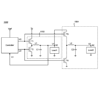
[0101] FIG. 10A is a schematic diagram of a "chained" feedback-regulated
voltage supply circuit
1000. The illustrated embodiment eliminates the need for separate regulator
circuits for each regulated
voltage. The illustrated regulated voltage supply circuit 1000 is designed to
automatically maintain a
substantially constant voltage V1 at a first node Ni for a first load, Loadl,
and maintain a substan-
tially constant voltage V2 at a second node N2 for a second load, Load2.
¨20 ¨
Date Recue/Date Received 2021-12-08
[0102] In greater detail, the illustrated regulated voltage supply circuit
1000 is a DC/DC (switch-
mode) type converter which steps down an applied high voltage to V1 (also
known as a "buck" con-
verter). In alternative embodiments, the regulated voltage supply circuit 1000
may be configured to
step up an applied source voltage (also known as a "boost" converter).
[0103] The regulated voltage supply circuit 1000 includes at least two
stages. In the illustrated
example, a first output stage 1002 includes two stacked switches Ti and T2
series coupled as shown
between a source voltage (high voltage VII) and a low voltage (typically
circuit ground). A first LC
circuit comprising an inductor Li and a capacitor Cl is coupled between the
junction of Ti and T2,
and Loadl. Similarly, a second output stage 1004 includes stacked switches T3
and T4 series coupled
as shown between a source voltage (V1 in this case) and a low voltage
(typically circuit ground). A
second LC circuit comprising an inductor L2 and a capacitor C2 is coupled
between the junction of
T3 and T3, and Load2. Additional similar output stages may be "chained" in a
like manner; for exam-
ple, a third stage may utilize V2 as its source voltage. In some embodiments,
all of the switches (T1-
T4 in this example) may be field effect transistors (FETs). In some
embodiments, the "top" switches
(Ti and T3 in this example) may be FETs, while the "bottom" switches (T2 and
T4 in this example)
may be Schottky diodes.
[0104] The regulated voltage supply circuit 1000 also includes a Controller
that provides a se-
quence of first control pulses HD (for "high drive") and a sequence of second
control pulses LD (for
"low drive"). The HD and LD control pulses are non-overlapping and
complementary to each other
(thus, their duty cycles are also complementary). In the illustrated example,
the HD control pulses are
connected to the control inputs (e.g., FET gates) of Ti and T3, while the LD
control pulses are con-
nected to the control inputs of T2 and T4 (see the discussion of FIG. 10B
below for an alternative
configuration). Note that if Schottky diodes are used for the "bottom"
switches (T2 and T4 in this ex-
ample), the diodes switch on their own based on the voltage polarity, and thus
the LD control pulses
are not needed.
[0105] The regulated voltage supply circuit 1000 further includes a
feedback loop from Ni to the
Controller that operates by comparing the actual voltage V1 at node Ni to a
reference voltage Vref.
The Controller adjusts the duty cycle of the HD and LD control pulses to
maintain V1 at the Vref tar-
get value. For example, if VH decreases, the feedback loop increases the duty
cycle of the HD control
pulses to allow VH to be coupled through Ti to Ni longer (in the case of a
duty-cycle-controlled
DC/DC converter) or more frequently (in the case of a frequency-controlled
switcher) to compensate
for the change. More generally, the Controller adjusts the duty cycle ("d") of
the control pulses to
achieve a target output voltage output V1, so V1 is substantially equal to
d*VH.
¨ 21 ¨
Date Recue/Date Received 2021-12-08
[0106] The regulation of V2 is chained to V1, and T3 and T4 are switched by
the HD and LD
control pulses at the same rate and at the same duty cycle as Ti and T2,
respectively, with regard to
FIG. 10A. Any level shifters or scaling circuitry that may be needed to
properly drive T3 and T4 are
not shown for simplicity. The same duty cycle d is thus applied to the chained
switches T3 and T4,
resulting in a voltage ratio V2/Vi being substantially the same as the voltage
ratio Vi/VH:
Vl/VH = d = V2N1 => V1 = d*VH and V2 = cr*VH EQ. 4
[0107] For example, if d= 'A. or 50%, V1 will be one-half of VH, and V2
will be one-half of V1
(i.e., one quarter of VII); for VH = 48V, in this example, V1 would be 24V and
V2 would be 12V (ig-
noring possible voltage output variations due to parasitic losses, such as in
the inductors, Li, L2).
[0108] FIG. 10B is a schematic diagram of an alternative "chained" feedback
regulated voltage
supply circuit 1020. In the illustrated example, the HD control pulses are
connected to the control in-
puts of Ti and T4, while the LD control pulses are connected to the control
inputs of T2 and T3 (with
offsets and scaling, if needed, for proper driving levels). Thus, compared to
FIG. 10A, the HD and LD
control pulse lines cross over each other, as indicated by the dashed oval X.
For this configuration, V2
= d*(1 ¨ d)*VH. In a variant configuration, by disconnecting T3 from Ni and
connecting the same ter-
minal of T3 to VH (i.e., feeding T3 from VH instead of from V1, but keeping
the "crossed" LD and
HD control pulse connections shown in FIG. 10B), then V2 = (1 ¨ d)*VH. In yet
another variant con-
figuration, by feeding T3 from VH but coupling the HD and LD control pulses as
shown in FIG. 10A,
then V2 = d*VH, which is essentially the same as Vi; this configuration may
useful to achieve greater
current capability at the same voltage without requiring larger switches (T1-
T4, in this example) and
higher inductor and capacitor sizes that may be needed in a single
(conventional) stage voltage supply
circuit. As should be clear, by inserting switches at appropriate locations to
control which control
pulses are applied to the control inputs of T3 and T4, and/or to control the
voltage inputs to T3, one
circuit can be fabricated that can output any of up to four different values
for V2: V2 = ct*VH; V2 =
cr*VH; V2 = d*(1 ¨ d)*VH; and/or V2 = (1 ¨ drVH.
[0109] The "chained" regulated voltage supply circuits of FIG. 10A or 10B,
and their variants,
thus provide at least two output voltage levels with only one Controller, thus
saving space and cost.
Such a circuit thus may be quite useful for embodiments of the circuit shown
in FIG. 9, which require
at least two voltage levels; for example, V1 may be used for \THIGH, and V2
may be used for VLow
(load would not be a factor in such an application, since only one load would
be connected at a time
due to the complementary states of the top and bottom switches in the switch
module 904). Further-
more, the "chaining" architecture can be extended by adding more stages in a
similar manner, each
new stage feeding off from the previous stage. For example, a third stage can
be chained to the second
¨22 ¨
Date Recue/Date Received 2021-12-08
stage 1004 by feeding off from V2 and being switched by HD. The third stage
would produce a volt-
age V3 that would be equal to cr*VH. Moreover, by inserting switches at
appropriate locations to con-
trol which control pulses are applied to the control inputs of the switches of
each stage, and/or to con-
trol the voltage inputs to each stage, one circuit can be fabricated that can
output even more supply
voltages at low cost.
[0110] Methods
[0111] Another aspect of the invention includes a method for biasing a
telecommunications sys-
tem transmitter circuit, comprising: receiving digital source information;
generating a modulated in-
formation signal from the received digital source information; generating a
dynamic input bias signal
as a function of the envelope of a form of the source information; combining
the modulated infor-
mation signal and the dynamic input bias signal; and outputting an analog
signal of the combined
modulated information signal and dynamic input bias signal, the analog signal
suitable to be applied
to an input of a power amplifier.
[0112] Yet another aspect of the invention includes a method for biasing a
telecommunications
system transmitter circuit, comprising: receiving digital source information;
generating a modulated
information signal from the received digital source information; generating a
dynamic input bias sig-
nal as a function of the envelope of a form of the source information;
combining the modulated infor-
mation signal and the dynamic input bias signal; outputting an analog signal
of the combined modu-
lated information signal and dynamic input bias signal; and coupling the
analog signal to the input of
a power amplifier, for amplification by the power amplifier.
[0113] Still another aspect of the invention is a method for biasing a
telecommunications system
transmitter circuit, comprising: receiving digital source information;
generating a modulated infor-
mation signal from the received digital source information; applying a
linearizing transform function
to the modulated information signal; applying a transform function to the
envelope of a form of the
source information to generate a pre-distorted envelope; generating a dynamic
input bias signal as a
function of the pre-distorted envelope; combining the linearized modulated
information signal and the
dynamic input bias signal; outputting an analog signal of the combined
linearized modulated infor-
mation signal and dynamic input bias signal; and coupling the analog signal to
the input of a power
amplifier, for amplification by the power amplifier.
[0114] Additional aspects of one or more of the above methods include:
applying a transform
function to the envelope of the source information before generating the
dynamic input bias signal,
such that the dynamic input bias signal is a pre-distorted dynamic input bias
signal; the transform
¨23 ¨
Date Recue/Date Received 2021-12-08
function applying a first pre-distortion level for envelope levels below a
selected threshold, and a sec-
ond pre-distortion level, less than the first pre-distortion level, for
envelope levels above the selected
threshold; the transform function being applied only to envelope levels below
a selected threshold; the
transform function being an inverse profile of a gain profile of the power
amplifier; receiving from a
remote gateway a calibration signal derived from signals transmitted by the
telecommunications sys-
tem transmitter circuit, and adjusting the transform function as a function of
the received calibration
signal; determining the pending occurrence of peaks in the envelope of the
information signal, and
outputting a supply voltage for the power amplifier, the supply voltage having
a voltage potential as a
function of the determined occurrence of pending peaks in the envelope of the
information signal; ad-
justing the transform function as a function of the supply voltage potential;
determining the occur-
rence of peaks in the envelope of the information signal that exceed at least
one selected threshold,
and outputting a first supply voltage to the power amplifier in response to
the determined occurrence
of peaks in the envelope of the information signal that exceed the at least
one selected threshold, and
otherwise outputting a second supply voltage to the power amplifier; adjusting
the transform function
as a function of the supply voltage output; applying a linearizing transform
function to the modulated
information signal; receiving from a remote gateway a calibration signal
derived from signals trans-
mitted by the telecommunications system transmitter circuit, and adjusting the
linearizing transform
function as a function of the received calibration signal; adding a selected
amount of DC bias to the
input of the power amplifier.
[0115] Another aspect of the invention includes a method for providing two
or more regulated
output voltages, comprising: providing a first output stage comprising stacked
transistors configured
to be coupled between a first voltage and a second voltage, each transistor
having a corresponding
control input, the first output stage configured to provide a first output
voltage at a first output node;
providing at least one subsequent output stage, each subsequent output stage
comprising stacked tran-
sistors configured to be coupled between (1) either the output node of a
previous output stage or the
first voltage and (2) the second voltage, each transistor having a
corresponding control input, each
subsequent output stage configured to provide a corresponding subsequent
output stage output voltage
at a corresponding output node; and providing a controller, configured to be
coupled to a reference
voltage and coupled to the first output voltage from the first output stage,
the controller outputting a
first output pulse signal and a non-overlapping and complementary second
output pulse signal,
wherein the first output pulse signal is coupled to the control input of one
of the two transistors in
each output stage, and the second output pulse signal is coupled to the
control input of the other of the
two transistors in each output stage, wherein the controller regulates the
duty cycles of the first and
second output pulse signals as a function of a comparison of the reference
voltage to the first output
voltage.
¨24 ¨
Date Recue/Date Received 2021-12-08
[0116] Still another aspect of the invention includes a method for
providing two regulated output
voltages, comprising: providing a first output stage comprising stacked field-
effect transistors (FETs)
configured to be coupled between a first voltage and ground, each FET having a
corresponding con-
trol input, the first output stage configured to provide a first output
voltage at a first node; providing a
second output stage comprising stacked FETs configured to be coupled between
(1) either the output
node of the first stage or the first voltage and (2) ground, each FET having a
corresponding control
input, the second output stage configured to provide a second output voltage
at a second output node;
and providing a controller, configured to be coupled to a reference voltage
and coupled to the first
output voltage from the first output stage, the controller outputting a first
output pulse signal and a
non-overlapping and complementary second output pulse signal, wherein the
first output pulse signal
is coupled to the control input of one of the two transistors in each of the
first and second output
stages, and the second output pulse signal is coupled to the control input of
the other of the two tran-
sistors in each of the first and second output stages, wherein the controller
regulates the duty cycles of
the first and second output pulse signals as a function of a comparison of the
reference voltage to the
first output voltage.
[0117] Additional aspects of one or more of the above methods for providing
regulated output
voltages include: each transistor being a field-effect transistor; and the
subsequent output stage output
voltage of a first of the at least one subsequent output stage being
approximately one of d*VH, cr*VH,
d*(1 ¨ d)* VH, or (1 ¨ d)* VH, where d is the duty cycle of the first and
second output pulse signals, and
VH is the first voltage.
[0118] Fabrication Technologies and Options
[0119] In practical implementations, modulating the input signal bias at
the envelope frequency
may produce spectral energy at the envelope frequency at the output of the PA
508. Accordingly, that
energy may need to be filtered out. A conventional output filter or matching
network can be used to
accomplish this filtering function; the wider the separation between the RF
carrier frequency and the
envelope frequency, the easier the filtering. In addition, anti-aliasing
filters and interface circuits be-
tween the DACs 504, 512 and the input of the PA 508 may be needed.
[0120] As should be readily apparent to one of ordinary skill in the art,
various embodiments of
the invention can be implemented to meet a wide variety of specifications.
Circuits that may be
needed for particular applications (such as for up or down frequency
conversion, voltage offsets, neg-
ative supply rail, etc.) are not shown for simplicity.
¨25 ¨
Date Recue/Date Received 2021-12-08
[0121] While the description above has focused on the transmitter circuitry
of user terminals 102
by way of example, the invention may be applied to transmitter circuitry
within a gateway 106 as well
to lower power consumption.
[0122] While the embodiments described above and illustrated in the figures
contain a variety of
elements shown as separate function blocks, the functionality of such blocks
may be integrated into
fewer blocks or more blocks. Unless otherwise noted above, selection of
suitable component values is
a matter of design choice and various embodiments of the invention may be
implemented in any suita-
ble IC technology (including but not limited to MOSFET and IGFET structures),
or in hybrid or dis-
crete circuit forms. Integrated circuit embodiments may be fabricated using
any suitable substrates
and processes, including but not limited to GaN, GaAs, standard bulk silicon,
silicon-on-insulator
(SOT), silicon-on-sapphire (SOS), and MESFET technologies.
[0123] The term "MOSFET" technically refers to metal-oxide-semiconductors;
another synonym
for MOSFET is "MISFET", for metal-insulator-semiconductor FET. However,
"MOSFET" has be-
come a common label for most types of insulated-gate FETs ("IGFETs"). Despite
that, it is well
known that the term "metal" in the names MOSFET and MISFET is now often a
misnomer because
the previously metal gate material is now often a layer of polysilicon
(polycrystalline silicon). Simi-
larly, the "oxide" in the name MOSFET can be a misnomer, as different
dielectric materials are used
with the aim of obtaining strong channels with smaller applied voltages.
Accordingly, the term
"MOSFET" as used herein is not to be read as literally limited to metal-oxide-
semiconductors, but in-
stead includes IGFETs in general.
[0124] Voltage levels may be adjusted or voltage and/or logic signal
polarities reversed depend-
ing on a particular specification and/or implementing technology (e.g., NMOS,
PMOS, or CMOS, and
enhancement mode or depletion mode transistor devices). Component voltage,
current, and power
handling capabilities may be adapted as needed, for example, by adjusting
device sizes, serially
"stacking" components (particularly FETs) to withstand greater voltages,
and/or using multiple com-
ponents in parallel to handle greater currents. Additional circuit components
may be added to enhance
the capabilities of the disclosed circuits and/or to provide additional
functional without significantly
altering the functionality of the disclosed circuits.
[0125] A number of embodiments of the invention have been described. It is
to be understood
that various modifications may be made without departing from the spirit and
scope of the invention.
For example, some of the steps described above may be order independent, and
thus can be performed
in an order different from that described. Further, some of the steps
described above may be optional.
Various activities described with respect to the methods identified above can
be executed in repetitive,
serial, or parallel fashion. It is to be understood that the foregoing
description is intended to illustrate
¨26 ¨
Date Recue/Date Received 2021-12-08
and not to limit the scope of the invention, which is defined by the scope of
the following claims, and
that other embodiments are within the scope of the claims. (Note that (1) as
used in this specification,
the accompanying figures, and the claims below, "comprising" is to be
interpreted as meaning "in-
cluding", "containing", "comprehending", and (2) the parenthetical labels for
claim elements are for
ease of referring to such elements, and do not in themselves indicate a
particular required ordering or
enumeration of elements; further, such labels may be reused in dependent
claims as references to ad-
ditional elements without being regarding as starting a conflicting labeling
sequence).
¨27 ¨
Date Recue/Date Received 2021-12-08