Note: Descriptions are shown in the official language in which they were submitted.
CA 03142014 2021-11-25
WO 2020/251900
PCT/US2020/036668
Implantable Medical Device Without a Wire-Wound Coil Configured to Receive
Wireless Power from an External Charger
FIELD OF THE INVENTION
[0001] The present invention relates to implantable medical devices and means
for wireless
receipt of power from an external charger.
BACKGROUND
[0002] Implantable stimulation devices are devices that generate and deliver
electrical stimuli
to body nerves and tissues for the therapy of various biological disorders,
such as pacemakers
to treat cardiac arrhythmia, defibrillators to treat cardiac fibrillation,
cochlear stimulators to
treat deafness, retinal stimulators to treat blindness, muscle stimulators to
produce
coordinated limb movement, spinal cord stimulators to treat chronic pain,
cortical and deep
brain stimulators to treat motor and psychological disorders, and other neural
stimulators to
treat urinary incontinence, sleep apnea, shoulder subluxation, etc. The
description that
follows will generally focus on the use of the invention within a Spinal Cord
Stimulation
(SCS) system, such as that disclosed in U.S. Patent 6,516,227. However, the
present
invention may find applicability in any implantable medical device system,
including a Deep
Brain Stimulation (DBS) system.
[0003] As shown in Figures 1A-1B, a SCS system typically includes an
Implantable Pulse
Generator (IPG) 10 (Implantable Medical Device (IMD) 10 more generally), which
includes
a biocompatible device case 12 formed of a conductive material such as
titanium for
example. The case 12 typically holds the control circuitry 86 (Fig. 3) and
battery 14 (Fig.
1B) necessary for the IMD 10 to function. The IMD 10 is coupled to electrodes
Ex 16 via
one or more electrode leads 18, such that the electrodes 16 form an electrode
array 20. The
electrodes 16 are carried on a flexible body 22, which also houses the
individual signal wires
24 coupled to each electrode. In the illustrated embodiment, there are eight
electrodes (Ex)
on two leads 18, although the number of leads and electrodes is application
specific and
therefore can vary. The leads 18 couple to lead connectors 26 in the IMD 10,
which are fixed
in a non-conductive header material 28 such as an epoxy. Feedthrough pins 23
connect to
electrode contacts (not shown) in the lead connectors 26, which pins pass
through a hermetic
feedthrough 25 on the top of the case 12, where they are connected to
stimulation circuitry
inside of the IMD 10's case. Control circuitry 86 can include stimulation
circuitry configured
1
CA 03142014 2021-11-25
WO 2020/251900
PCT/US2020/036668
to provide stimulation current to selected ones of the electrodes, and can
comprise circuitry
disclosed for example in USPs 6,181,969, 8,606,362, 8,620,436, U.S. Patent
Application
Publications 2018/0071520 and 2019/0083796. The conductive case 12 material
can also
operate as a case electrode Ec to provide a return current path for currents
provided at the
lead based electrodes, Ex.
[0004] As shown in the cross-section of Figure 1B, the IMD 10 typically
includes a printed
circuit board (PCB) 29, along with various electronic components 32 mounted to
the PCB 29,
some of which are discussed subsequently. The IMD 10 traditionally includes a
charging coil
30 for charging or recharging the IMD's battery 14 using an external charger.
The case 12 is
typically formed of two clam-shell-like portions 12i and 12o that that are
designed when
implanted to respectively face the inside and outside of the patient. These
portions 12i and
12o are typically welded (11) together along the outer periphery of the case,
and include
flanges that are welded to the feedthrough 25. When so formed, the case 12
includes planar
parallel major surfaces formed in the outside and inside case portions 12o and
12i, and a
generally planar top surface 12t perpendicular to the major surfaces which
includes the
feedthrough 25.
[0005] Figures 2A and 2B show the IMD 10 in communication with external
chargers, and
two different examples of chargers 40 and 60 are shown. Both types of chargers
40 and 60
are used to wirelessly convey power in the form of an electromagnetic field 55
(referred to as
a "magnetic field" for short) to the IMD 10, which power can be used to
recharge the IMD's
battery 14. The transfer of power from external charger 40 is enabled by a
primary charging
coil 44 in Figure 2A, and by a primary charging coil 66 in Figure 2B. Figure
2A shows an
example in which the charging coil 44 is integrated in the same housing as
other charger
electronics, while in Figure 2B the charging coil 66 and charger electronics
are separated into
different housings and connected by a cable 68.
[0006] In Figure 2A, the integrated charger 40 includes a PCB 46 on which
electronic
components 48 are placed, some of which are discussed subsequently. Charging
coil 44 may
be mounted to the PCB 46, and preferably on the side of the PCB that faces the
IMD 10 as
shown. A user interface, including touchable buttons, LEDs (not shown) and
perhaps a
display and a speaker (not shown), allows a patient or clinician to operate
the external charger
40. In Figure 2A, the user interface is shown simply as including an on/off
button 42 used to
turn the magnetic field 55 on or off A battery 50 provides power for the
external charger 40,
which battery 50 may itself be rechargeable. Charger 40 is typically
configured to be hand-
holdable and portable, and is described further in U.S. Patent Application
Publication
2
CA 03142014 2021-11-25
WO 2020/251900
PCT/US2020/036668
2017/0361113.
[0007] In Figure 2B, the charger 60 comprises a charging coil assembly 62 and
an
electronics module 64 in separate housings which are connected by a cable 68.
The charging
coil assembly 62 includes the charging coil 66, while the electronics and user
interface
elements are provided by the electronics module 64. The electronics housing 64
may include
a PCB 70, a battery 72, various control circuitry 74, and user interface
elements 76 such as
those mentioned above. Charger 60 despite generally being in two pieces 62 and
64 is also
typically configured to be hand-holdable and portable, and is again described
further in the
above-referenced 2017/0361113 publication.
[0008] Transmission of the magnetic field 55 from either of chargers 40 or 60
to the IMD 10
occurs wirelessly and transcutaneously through a patient's tissue via
inductive coupling.
Figure 3 shows details of the circuitry used to implement such functionality.
Primary
charging coil 44 or 66 in the external charger is energized via charging
circuit 64 with an AC
current, Icharge, to create the AC magnetic charging field 55. A tuning
capacitor 45 is
provided to form a resonant LC tank with the charging coil 44 or 66, which
generally sets the
frequency of the AC magnetic field 55.
[0009] The magnetic portion of the electromagnetic field 55 induces a current
Icoil in the
secondary charging coil 30 within the IMD 10, which current is received at
power reception
circuitry 81. Power reception circuitry 81 can include a tuning capacitor 80,
which is used to
tune the resonance of the LC circuit in the IMD to the frequency of the
magnetic field. One
skilled will understand that the capacitors 45 or 80 may be placed in series
or in parallel with
their respective coils (inductances) 44/66 or 30, although it is preferred
that the capacitor 45
be placed in series with the coil 44/66 in the charger 40/60, while the
capacitor 80 is placed in
parallel with the coil 30 in the IMD 10. The power reception circuitry 81
further includes a
rectifier 82 used to convert AC voltage across the coil 30 to DC a DC voltage
Vdc. Power
reception circuitry 81 may further include other conditioning circuitry such
as charging and
protection circuitry 84 to generate a Voltage Vbat which can be used to
provide regulated
power to the IMD 10, and to generate a current Ibat which is used to charge
the battery 14.
The frequency of the magnetic field 55 can be perhaps 80 kHz or so.
[0010] The IMD 10 can also communicate data back to the external charger 40 or
60, and
this can occur in different manners. As explained in the above-referenced
2017/0361113
publication, the IMD 10 may employ reflected impedance modulation to transmit
data to the
charger, which is sometimes known in the art as Load Shift Keying (LSK), and
which
involves modulating the impedance of the charging coil 30 with data bits
provided by the
3
CA 03142014 2021-11-25
WO 2020/251900
PCT/US2020/036668
IMD 10's control circuitry 86. The IMD may also use a communications channel
separate
from that used to provide power to transmit data to the charger, although such
alternative
channel and the antenna required are not shown for simplicity. The charger 40
or 60 can
include demodulation circuitry 68 to recover the transmitted data, and to send
such data to the
charger's control circuitry 72. Such data as telemetered from to the charger
40/60 from the
IMD 10 can include information useful for the charger to know during charging,
such as the
IMD's temperature (as sensed by temperature sensor 87), the voltage Vbat of
the IMD's
battery 14, or the charging current Ibat provided to the battery. Charger
40/60 can use such
telemetered data to control production of the magnetic field 55, such as by
increasing or
decreasing the magnitude of the magnetic field 55 (by increasing or decreasing
Icharge), or
by starting or stopping generation of the magnetic field 55 altogether. As
explained in the
above-referenced 2017/0361113 publication, the charger 40/60 may also be used
to determine
the alignment of the charging coil 44/66 to the IMD 10, and may include
alignment indicators
(LEDs or sounds) that a user can review to determine how to reposition the
charger to be in
better alignment with the IMD 10 for more efficient power transfer.
SUMMARY
[0011] An implantable medical device (IMD) configured to wirelessly receive
power from an
electromagnetic field is disclosed, which may comprising: a case housing
control circuitry for
the IMD, wherein at least a portion of the case is conductive, and wherein a
case current is
formed in the conductive case portion in response to the electromagnetic
field; power
reception circuitry inside the case; and first and second electrical
connections to divert at least
some of the case current as a power current to the power reception circuitry,
wherein the
power reception circuitry is configured to use the power current to provide
power to the IMD.
[0012] In one example, the IMD further comprises a non-conductive header
affixed to the
case. In one example, at least one of the first and second electrical
connections comprises an
antenna portion in or on the header, resulting in at least one antenna portion
in or on the
header. In one example, the IMD further comprises one or more lead connectors
in the
header, a feedthrough between the header and the case, and a plurality of
electrode
feedthrough wires, wherein the electrode feedthrough wires connect to contacts
in the lead
connectors and pass through the feedthrough inside the case. In one example,
at least one of
the first and second electrical connections comprises a feedthrough wire
connected to the at
least one antenna portion that passes through the feedthrough. In one example,
the at least
one antenna portion is formed of a material of the case. In one example, the
case comprises a
4
CA 03142014 2021-11-25
WO 2020/251900
PCT/US2020/036668
planar surface configured to face an outside of a patient when implanted,
wherein the at least
one antenna portion is offset in or on the header towards the outside planar
surface. In one
example, there is a first antenna portion in or on the header comprising the
first electrical
connection, and a second antenna portion in or on the header comprising the
second electrical
connection. In one example, the first antenna portion comprises a first end
and a second end,
and wherein the second antenna portion comprises a first end and a second end.
In one
example, the first electrical connection further comprises a first wire
connected to the first
end of the first antenna portion, wherein the second end of the first antenna
portion is
connected to the conductive case portion, wherein the second electrical
connection further
comprises a second wire connected to the first end of the second antenna
portion, wherein the
second end of the second antenna portion is connected to the conductive case
portion. In one
example, there is a single antenna portion in or on header comprising the
first electrical
connection. In one example, the single antenna portion comprises a first end
and a second
end, wherein the first electrical connection further comprises a first wire
connected to the first
end of the single antenna portion, wherein the second end of the single
antenna portion is
connected to the conductive case portion. In one example, the second
electrical connection
comprises a second wire connected to the conductive case portion. In one
example, there is a
single antenna portion in or on the header comprising the first electrical
connection and
second electrical connection. In one example, the single antenna portion
comprises a cross
member connected to the conductive case portion along its length. In one
example, the first
electrical connection comprises a first wire connected to a first end of the
single antenna
portion, and wherein the second electrical connection a second wire connected
to a second
end of the single antenna portion. In one example, the single antenna portion
comprises a
cross member connected to the conductive case portion at first contact and at
a second
contact, wherein there is a space between the cross member and the case
between the first and
second contacts. In one example, the first electrical connection comprises the
first contact
and a first wire connected to a first end of the single antenna portion, and
wherein the second
electrical connection comprises the second contact and a second wire connected
to a second
end of the single antenna portion. In one example, the first and second
connections are not
formed in or on the header. In one example, at least one of the first and
second electrical
connections comprises a wire connected to the conductive case portion. In one
example, the
first electrical connection comprises a first wire connected to the conductive
case portion at a
first contact, and wherein the second electrical connection comprises a second
wire connected
to the conductive case portion at a second contact. In one example, the first
and second
CA 03142014 2021-11-25
WO 2020/251900
PCT/US2020/036668
electrical connections are separated by a portion of the case having a first
conductivity, and
wherein the conductive case portion in which the case current is formed has a
second
conductivity higher than the first conductivity. In one example, the power
reception circuitry
comprises a rectifier configured to convert the power current to a DC voltage
that is used to
provide power to the IMD. In one example, the IMD further comprises a battery
within the
case, wherein the power reception circuitry is configured to use the power
current to provide
power to the IMD to charge the battery. In one example, the conductive case
portion
comprises a conductive layer applied to the case. In one example, the IMD does
not include
a header. In one example, the case comprises a dielectric material, and
wherein the
conductive case portion comprises a conductive window. In one example, the
dielectric
material comprises a ceramic. In one example, conductive window is affixed to
the dielectric
material in a manner to cover a hole in the dielectric material. In one
example, the
conductive window comprises a plate affixed on or in the dielectric material.
In one
example, the control circuitry further comprises stimulation circuitry to form
stimulation
currents at selected ones of a plurality of electrodes in contact with a
patient's tissue, wherein
the conductive window comprises one of the plurality of electrodes. In one
example, the
conductive window is configured to be in contact with a patient's tissue, and
is further
configured to operate as a case electrode. In one example, the power reception
circuitry is
not coupled to a wire-wound coil configured to receive the electromagnetic
field.
[0013] An implantable medical device (IMD) configured to wirelessly receive
power from an
electromagnetic field is disclosed, which may comprise: a case housing control
circuitry for
the IMD, wherein at least a portion of the case is conductive, and wherein a
case current is
formed in the conductive case portion in response to the electromagnetic
field; power
reception circuitry inside the case; a non-conductive header affixed to the
case; and first and
second electrical connections to divert at least some of the case current as a
power current to
the power reception circuitry, wherein the first electrical connection
comprises a first antenna
portion in or on the header and wherein the second electrical connection
comprises a second
antenna portion in or on the header, wherein the power reception circuitry is
configured to
use the power current to provide power to the IMD.
[0014] In one example, the IMD further comprises one or more lead connectors
in the header,
a feedthrough between the header and the case, and a plurality of electrode
feedthrough
wires, wherein the electrode feedthrough wires connect to contacts in the lead
connectors and
pass through the feedthrough inside the case. In one example, the first
electrical connection
comprises a first feedthrough wire connected to the first antenna portion that
passes through
6
CA 03142014 2021-11-25
WO 2020/251900
PCT/US2020/036668
the feedthrough, wherein the second electrical connection comprises a second
feedthrough
wire connected to the second antenna portion that passes through the
feedthrough. In one
example, the first and second antenna portions are formed of a material of the
case. In one
example, the case comprises a planar surface configured to face an outside of
a patient when
implanted, wherein the first and second antenna portions are offset in or on
the header
towards the outside planar surface. In one example, the first antenna portion
comprises a first
end and a second end, and wherein the second antenna portion comprises a first
end and a
second end. In one example, the first electrical connection further comprises
a first wire
connected to the first end of the first antenna portion, wherein the second
end of the first
antenna portion is connected to the conductive case portion, wherein the
second electrical
connection further comprises a second wire connected to the first end of the
second antenna
portion, wherein the second end of the second antenna portion is connected to
the conductive
case portion. In one example, the first wire and the second wire pass through
a feedthrough
in the case. In one example, the first wire and the second wire are connected
to the first ends
of the first and second antenna portions through one or more openings in case.
In one
example, the case comprises a planar surface configured to face an outside of
a patient when
implanted, wherein the one or more openings are formed in the planar surface.
In one
example, the second ends of the first and second antenna portions are
connected to a top of
the case. In one example, the case comprises a planar surface configured to
face an outside
of a patient when implanted, wherein the second ends of the first and second
antenna portions
are connected to the planar surface. In one example, the power reception
circuitry comprises
a rectifier configured to convert the power current to a DC voltage that is
used to provide
power to the IMD. In one example, the IMD further comprises a battery within
the case,
wherein the power reception circuitry is configured to use the power current
to provide power
to the IMD to charge the battery. In one example, the conductive case portion
comprises a
conductive layer applied to the case. In one example, the conductive layer is
also applied to
the first and second antenna portions. In one example, the conductive layer is
applied inside
the case. In one example, the case comprises a window of material different
from a material
of the case, wherein a conductivity of the window material is less than a
conductivity of the
material of the case. In one example, the conductive case portion at least
partially surrounds
the window. In one example, the case comprises a planar surface configured to
face an
outside of a patient when implanted, wherein the window is formed in the
planar surface. In
one example, the power reception circuitry is not coupled to a wire-wound coil
configured to
receive the electromagnetic field.
7
CA 03142014 2021-11-25
WO 2020/251900
PCT/US2020/036668
[0015] An implantable medical device (IMD) configured to wirelessly receive
power from an
electromagnetic field is disclosed, which may comprise: a case housing control
circuitry for
the IMD, wherein at least a portion of the case is conductive, and wherein a
case current is
formed in the conductive case portion in response to the electromagnetic
field; power
reception circuitry inside the case; a non-conductive header affixed to the
case; and first and
second electrical connections to divert at least some of the case current as a
power current to
the power reception circuitry, wherein at least the electrical connection
comprises a single
antenna portion in or on the header, wherein the power reception circuitry is
configured to
use the power current to provide power to the IMD.
[0016] In one example, the IMD further comprises one or more lead connectors
in the header,
a feedthrough between the header and the case, and a plurality of electrode
feedthrough
wires, wherein the electrode feedthrough wires connect to contacts in the lead
connectors and
pass through the feedthrough inside the case. In one example, at least one of
the first and
second connections comprises a feedthrough wire connected to the single
antenna portion that
passes through the feedthrough. In one example, the single antenna portion is
formed of a
material of the case. In one example, the case comprises a planar surface
configured to face
an outside of a patient when implanted, wherein the single antenna portion is
offset in or on
the header towards the outside planar surface. In one example, the single
antenna portion
comprises only the first electrical connection but not the second electrical
connection. In one
example, the single antenna portion comprises a first end and a second end,
wherein the first
electrical connection further comprises a first wire connected to the first
end of the single
antenna portion, wherein the second end of the single antenna portion is
connected to the
conductive case portion. In one example, the second electrical connection
comprises a
second wire connected to the conductive case portion. In one example, the
single antenna
portion in or on the header comprises the first electrical connection and
second electrical
connection. In one example, the single antenna portion comprises a cross
member connected
to the conductive case portion along its length. In one example, the first
electrical connection
comprises a first wire connected to a first end of the single antenna portion,
and wherein the
second electrical connection comprises a second wire connected to a second end
of the single
antenna portion. In one example, the single antenna portion comprises a cross
member
connected to the conductive case portion at first contact and at a second
contact, wherein
there is a space between the cross member and the case between the first and
second contacts.
In one example, the first electrical connection comprises the first contact
and a first wire
connected to a first end of the single antenna portion, and wherein the second
electrical
8
CA 03142014 2021-11-25
WO 2020/251900
PCT/US2020/036668
connection comprises the second contact and a second wire connected to a
second end of the
single antenna portion. In one example, the power reception circuitry
comprises a rectifier
configured to convert the power current to a DC voltage that is used to
provide power to the
IMD. In one example, the IMD further comprises a battery within the case,
wherein the
power reception circuitry is configured to use the power current to provide
power to the IMD
to charge the battery. In one example, the conductive case portion comprises a
conductive
layer applied to the case. In one example, the conductive layer is also
applied to the single
antenna portions. In one example, the conductive layer is applied inside the
case. In one
example, the case comprises a window of material different from a material of
the case,
wherein a conductivity of the window material is less than a conductivity of
the material of
the case. In one example, the conductive case portion at least partially
surrounds the window.
In one example, the case comprises a planar surface configured to face an
outside of a patient
when implanted, wherein the window is formed in the planar surface. In one
example, the
power reception circuitry is not coupled to a wire-wound coil configured to
receive the
electromagnetic field.
[0017] An implantable medical device (IMD) configured to wirelessly receive
from power an
electromagnetic field is disclosed, which may comprise: a case housing control
circuitry for
the IMD, wherein at least a portion of the case is conductive, and wherein a
case current is
formed in the conductive case portion in response to the electromagnetic
field; power
reception circuitry inside the case; first and second electrical connections
to divert at least
some of the case current as a power current to the power reception circuitry,
wherein the first
electrical connection comprises a first contact made to the conductive case
portion, and
wherein the second electrical connection comprises a second contact made to
the conductive
case portion, wherein the power reception circuitry is configured to use the
power current to
provide power to the IMD.
[0018] In one example, the IMD further comprises a non-conductive header
affixed to the
case. In one example, the IMD further comprises one or more lead connectors in
the header,
a feedthrough between the header and the case, and a plurality of electrode
feedthrough
wires, wherein the electrode feedthrough wires connect to contacts in the lead
connectors and
pass through the feedthrough inside the case. In one example, the first and
second
connections are not formed in or on the header. In one example, the first
electrical
connection comprises a first wire connected to the conductive case portion at
the first contact,
and wherein the second electrical connection comprises a second wire connected
to the
conductive case portion at the second contact. In one example, the first and
second contacts
9
CA 03142014 2021-11-25
WO 2020/251900
PCT/US2020/036668
are separated by a portion of the case having a first conductivity, and
wherein the conductive
case portion in which the case current is formed has a second conductivity
higher than the
first conductivity. In one example, the conductive case portion comprises a
conductive layer
applied to the case. In one example, the conductive layer is applied outside
the case. In one
example, the conductive layer is applied inside the case. In one example, the
portion of the
case having the first conductivity comprises a window of material different
from a material of
the case. In one example, the conductive case portion at least partially
surrounds the window.
In one example, the case comprises a planar surface configured to face an
outside of a patient
when implanted, wherein the window is formed in the planar surface. In one
example, the
window comprises a dielectric material, and the conductive case portion
comprises a metallic
material. In one example, the window and the conductive case portions comprise
metallic
materials. In one example, the first contact is made to an outside of the
conductive case
portion through an opening in the conductive case portion, and wherein the
second contact is
made to the outside of the conductive case portion through an opening in the
conductive case
portion. In one example, the first and contact contacts respectively include
conductive pins.
In one example, the first contact is made to an inside of the conductive case
portion, and
wherein the second contact is made to the inside of the conductive case
portion. In one
example, the power reception circuitry comprises a rectifier configured to
convert the power
current to a DC voltage that is used to provide power to the IMD. In one
example, the IMD
further comprises a battery within the case, wherein the power reception
circuitry is
configured to use the power current to provide power to the IMD to charge the
battery. In
one example, the IMD does not include a header. In one example, the case
comprises a
dielectric material, and wherein the conductive case portion comprises a
conductive window.
In one example, the dielectric material comprises a ceramic. In one example,
the conductive
window is affixed to the dielectric material in a manner to cover a hole in
the dielectric
material. In one example, the conductive window comprises a plate affixed on
or in the
dielectric material. In one example, the control circuitry further comprises
stimulation
circuitry to form stimulation currents at selected ones of a plurality of
electrodes in contact
with a patient's tissue, wherein the conductive window comprises one of the
plurality of
electrodes. In one example, the conductive window is configured to be in
contact with a
patient's tissue, and is further configured to operate as a case electrode. In
one example, the
power reception circuitry is not coupled to a wire-wound coil configured to
receive the
electromagnetic field.
CA 03142014 2021-11-25
WO 2020/251900
PCT/US2020/036668
BRIEF DESCRIPTION OF THE DRAWINGS
[0019] Figures 1A and 1B show different views of an implantable pulse
generator, a type of
implantable medical device (IMD), in accordance with the prior art.
[0020] Figures 2A and 2B show different examples of external charger used to
wirelessly
charge a battery in an IMD or to provide power to the IMD.
[0021] Figure 3 shows relevant charging circuitry in the external chargers and
the IMD, in
accordance with the prior art.
[0022] Figures 4A-4D show first examples of an improved IMD without a wire-
wound coil
but capable of receiving wireless power from an external charger by harnessing
Eddy
currents generated in the IMD's conductive case, in which one or more antenna
portions are
provided in the IMD's header region.
[0023] Figure 5 shows a second example of the improved IMD, in which the
antenna
portions are differently connected to the IMD's case.
[0024] Figures 6A-6C show third examples of the improved IMD, which uses a
single
antenna portion.
[0025] Figure 7 shows a fourth example of the improved IMD, in which the
antenna portions
are formed using the material of the case.
[0026] Figure 8 shows a fifth example of the improved IMD, in which a
conductive layer is
used to accentuate the flow of Eddy currents.
[0027] Figure 9 shows a sixth example of the improved IMD, in which a lower-
conductivity
window in the case is used to accentuate the flow of Eddy currents.
[0028] Figures 10A and 10B show a seventh example of the improved IMD, which
does not
use antenna portions in the header region, but which uses a conductive layer
to accentuate the
flow of Eddy currents.
[0029] Figure 11 shows an eighth example of the improved IMD, which does not
use antenna
portions in the header region, but which uses a lower-conductivity window in
the case to
accentuate the flow of Eddy currents.
[0030] Figures 12A-12C show ninth examples of the improved IMD in a small form
factor.
[0031] Figure 13 shows a tenth example of the improved IMD, which includes two
conductive case modules.
[0032] Figure 14 shows an eleventh example of the improved IMD, which lacks a
header
attached to the case.
11
CA 03142014 2021-11-25
WO 2020/251900
PCT/US2020/036668
DETAILED DESCRIPTION
[0033] The inventors see room for improvement in wireless charging of IMDs. In
particular,
the inventors find unfortunate that traditional IMDs like IMD 10 require a
mechanically wire-
wound secondary coil 30 to pick up the magnetic field 55. Such coils are
relatively
expensive, difficult to work with, and can suffer from reliability problems.
Typically such
charging coils 30 are made from multi-stranded copper Litz wire, which
increases wire
conductivity and improves AC performance, but is complicated and expensive.
Such coils 30
are typically wound and formed on a mandrel prior to being assembled in the
IMD 10. It can
be difficult to connect the coil 30 to the PCB 29, and this connection can
break and become
unreliable. Further, a coil 30 can take significant volume in the IMD's case
12, which can
hamper making IMDs 10 smaller and more convenient for patients. The inventors
desire to
provide an IMD that is capable of wirelessly receiving power from an external
charger, but
which does not include a wire-wound coil 30.
[0034] The inventors notice that the IMD 10's case 12 is typically conductive
as already
mentioned, and as such it is reactive to the incoming magnetic field 55.
Specifically, the
magnetic portion of the AC magnetic field 55 will induce AC Eddy currents in
the case 12.
As is known, Eddy currents comprise loops of electrical current induced within
conductive
materials, in accordance with Faraday's law of induction. Eddy currents flow
in closed loops
in planes perpendicular to the magnetic field 55, and as such will flow
significantly in the
outside case portion 12o of the IMD that faces the external charger. The
magnitude of the
current in a given loop is proportional to the strength of the magnetic field,
the area of the
loop, and the rate of change of flux, and is proportional to the conductivity
of the material.
Eddy currents flow in conductive materials with a skin depth, and as such are
more prevalent
at the outside surface of the outer case portion 12o that face the impinging
magnetic field 55.
[0035] Eddy currents are generally viewed as an unwanted effect when charging
an IMD.
Some of the power in the field 55 is lost in the case 12 when Eddy current are
induced, thus
reducing the power that reaches the charging coil 30 inside the case. In
short, the case 12
generally attenuates the power that is able to reach the coil 30 to useful
effect to charge the
IMD's battery 14. Further, Eddy currents generated in the case 12 are
generally lost as heat,
and thus charging by magnetic induction runs the risk that the case may
overheat, which is a
unique safety problem when one considers that the IMD 10 is designed for
implantation
inside of a patient.
[0036] Despite such conventional wisdom, it is the inventors' desire to
provide an improved
IMD which harnesses the power of Eddy currents generated at least in part in
the IMD's case
12
CA 03142014 2021-11-25
WO 2020/251900
PCT/US2020/036668
12 during magnetic inductive charging, and to use such harnessed power to
charge the IMD's
battery 14 (or more generally to provide power to the IMD). In so doing, the
inventors'
improved IMD design does not require a wire-wound secondary charging coil 30,
which
alleviates manufacturing cost and complexity and reduces reliability issues
inherent when
using wire-wound coils. Further, the lack of a secondary charging coil 30
allows the IMDs to
be made smaller and more convenient for patients.
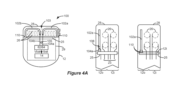
100371 A first example of such an improved IMD 100 is shown in Figure 4A. In
this
example, antenna portions 102a and 102b are included within the IMD 100's
header 28. It is
useful to note at this point that such antenna portions are not strictly
required in all
embodiments, as explained later starting with Figure 10A.
[0038] The antenna portions 102a and 102b are not wound coils, and are
preferably not made
of wire, although they could be. Instead, the antenna portions 102a and 102b
are preferably
formed from sheet metal into the shapes shown. The portions 102a and 102b are
preferably
conductive, and may be made from any number of conductive materials or alloys,
such as
those containing titanium, copper, gold, silver, and the like. The portions
102a and 102b may
also include combinations of alloys formed in distinctive layers, and in this
regard, the
portions may be coated, plated, or cladded with conductive materials, as
discussed further
subsequently.
[0039] In the example of Figure 4A, the antenna portions 102a and 102b are
generally C-
shaped, with outside ends attached to the case 12 (110), and with inside ends
attached to
antenna feedthrough wires 104a and 104b respectively. More specifically, and
as shown in
the cross sectional figure to the right, the outside ends of the portions 102a
and 102b (only
portion 102a is shown) are mechanically and electrically connected to the top
surface 12t of
the case, and more specifically to the top surface 12t of the outside case
portion 12o. Such
attachment may be made by welding or brazing the outside ends to the top
surface 12t, as
represented by weld 110. The left cross sectional figure shows the inside ends
of the portions
102a and 102b (again, only 102a shown), and shows attachment of the inside
ends to the
antenna feedthrough wires 104a and 104b (only 104a shown), which attachments
may be
made via a solder or weld 108. In this example, the antenna feedthrough wires
104a and
104b pass through the same feedthrough 25 as the electrode feedthrough wires
23 that
connect to the electrode contacts in the lead connectors 26. This example
shows four lead
connectors 26 arranged in a 2x2 fashion in the header 28, but more or fewer
lead connectors
could be used.
[0040] As shown in the cross sections of Figure 4A, the antenna portions 102a
and 102b are
13
CA 03142014 2021-11-25
WO 2020/251900
PCT/US2020/036668
preferably offset in the header 28 towards the major surface of outside case
portion 12o (to
the left as shown) of the IMD 100, with the lead connectors 26 in the header
being offset
towards the major surface of the inside case portion 12i (to the right). This
is preferred to
bring the antenna portions 102a and 102b closer to the external charger's
magnetic field 55,
and to minimize interference of conductive structures in the lead connectors
26 with magnetic
field reception. Once the lead connectors 26 are attached to the electrode
feedthrough wires
23, and the antenna portions 102a and 102b are connected to the case 12 and to
the antenna
feedthrough wires 104a and 104b, the header 28 can be formed over these
structures, such as
by encapsulation or overmolding with a suitable header material, e.g., a
polymer, epoxy, or
thermoset plastic. However, it is not strictly necessary for proper
functioning that the antenna
portions 102a and 102b be located in the header 28, or encapsulated within the
header
material. For example, the antenna portions 102 and 102b may also extend from,
or be on the
outer surface of, the header 28. The header 28 may not include lead connectors
in IMD
designs that do not require leads.
[0041] Further details of the circuitry and the formation of a current Ipower
used to provide
power to the IMD 100 are shown in Figure 4B. As discussed above, the magnetic
field 55
will induce Eddy currents in the conductive case 12. These circular currents
will tend to
oppose one another in the center of the case, but will reinforce each other
towards the case's
periphery, giving rise to a current, Icase, with a highest current density
proximate to the
periphery as shown. This current Icase would generally return as current Ix
towards the top
of the case.
[0042] However, at least some (and in other designs, possibly all) of the
current Icase will
also be diverted via the electrical connections 110 and to the antenna
portions 102a and 102b
as current Ipower. The flow of current Ipower is facilitated in different
ways. First, the
outside ends of the antenna portions 102a and 102b are connected (110)
proximate to the
periphery of case 12 where Icase is highest. Second, the antenna portions 102a
and 102b are
preferably formed of high conductivity (low resistance) materials, as
described above. In this
regard, it is preferable that the antenna portions 102a and 102b (e.g.,
silver) have a higher
conductivity than the conductive material used to form the case (e.g.,
titanium), which
bolsters the magnitude of Ipower relative to return current Ix. Third, as
noted just discussed,
the preference for Eddy currents to flow to the periphery of conductive
structures means that
current will preferably flow through the antenna portions 102a and 102b, which
are more
peripheral in the IMD 100 than the case portion where return current Ix is
formed. In short,
and through these means, a significant AC current Ipower is generated, which
may be on the
14
CA 03142014 2021-11-25
WO 2020/251900
PCT/US2020/036668
order of 0.5 to 3.0 Amps and suitable for charging the battery 14.
[0043] The antenna feedthrough wires 104a and 104b are connected to the
antenna portions
102a and 102b, and are connected to the PCB 29 inside the case 12 to provide
Ipower to
power reception circuitry 101. Power reception circuitry 101 as before can
include a tuning
capacitor 105, which can be serially connected but is shown in parallel
between the antenna
feedthrough wires 104a and 104. The capacitance value of the tuning capacitor
105 can be
modified to tune reception to the frequency of the magnetic field 55, as
discussed further
below. A rectifier 82 as before can derive a DC voltage Vdc, which can
optionally be
provided to charging and protection circuitry 84 used to derive Vbat and Ibat
to charge the
IMD 100's battery 14, or more generally to provide power to the IMD 100.
[0044] In short, first and second electrical connections divert at least some
of Icase as
Ipower, thus allowing the power reception circuitry 101 to use Ipower to
provide power to the
IMD. These electrical connections can include different structures, such as
antenna portions,
wires, contacts, or combinations of these, as explained in other various
embodiments below.
[0045] In the example of Figure 4A, the antenna portions 102a and 102b are
similarly sized,
and include a gap 103 between them, which gap 103 is generally centered from
left to right in
the IMD 100. However, the antenna portions 102a and 102b may be of different
sizes, and
the gap 103 may be provided in different positions without affecting the
current paths used to
form Ipower. For example, in IMD 100' of Figure 4C, the gap 103 has been moved
to the
left, and thus antenna portion 102b is smaller than antenna portion 102a.
[0046] In IMD 100" of Figure 4D, only a single antenna portion 102 is present
in the header
28 region, having a right end affixed to the top surface 12t of the case
(110), and having a
free end attached to antenna feedthrough wire 104a as before. Antenna wire
104b in this
example does not pass through the feedthrough 25, but instead is connected 107
to the outside
case portion 12o. Such connection 107 can be established in different ways as
shown in
Figure 4D's cross sections. In the left cross section, the antenna wire 104b
is connected to
the inside surface of the outside case portion 12o, i.e., inside the case, at
a solder or weld 111.
In the right cross section, the antenna wire 104b ultimately makes an
electrical connection
with the outside surface of the outside case portion 12o. This is facilitated
by use of a
conductive pin 113 which passes through an opening (not labeled) in the major
surface of the
outer case portion 12o. This pin 113 can be welded to the outside surface, and
welded inside
the case to the antenna wire 104b. Connection 107 in the right cross section
may be preferred
over the left cross section as more conducive to increasing the magnitude of
Ipower. This is
because Eddy currents as noted earlier will tend to form on the outside
surface of the outside
CA 03142014 2021-11-25
WO 2020/251900
PCT/US2020/036668
case portion 12o (via the skin depth phenomenon), which pin 113 in the right
cross section
connects to directly. When connection 107 is established on the inside surface
as in the left
cross section, the thickness of the outside case portion 12o intervenes
between the Eddy
currents on the outside surface and the connection 107 on the inside surface,
creating a bulk
resistance which could adversely affect the flow of Ipower. Extra steps may be
desirable to
ensure that connection 107 as shown in the right cross section is suitably
hermetic to prevent
fluid ingress. For example, and as discussed in other examples below, the pin
113 may be
fixed in the opening in the outside case portion 12o using a glass ferrule,
and/or the header 28
may be overmolded so as to cover the connection.
[0047] In any event, in IMD 140", and regardless of the means by which
connection 107 is
connected to the case 12, the circuit is effectively the same as described in
Figure 4B: some
amount of Icase is provided to the capacitor 105 and related circuitry (not
shown) as Ipower
via antenna wire 104b, while antenna wire 104a and antenna portion 102 return
Ipower back
to Icase.
[0048] Figure 5 shows another example of an improved IMD 120 having antenna
portions
122a and 122b, which differs from the previous example in the manner in which
the antenna
portions are connected. In this example, and as best seen in the cross
sections, the antenna
portions 122a and 122b are connected to the major surface of the outside case
portion 12o,
rather than to the top surface 12t. The right cross section shows connection
of the outside
ends of the antenna portions (only 122a shown) at the periphery of the case,
and shows that
the outside ends have been welded (128) to the major surface of the outside
case portion 12o
to establish an electrical connection.
[0049] The left cross section shows the inside ends of the antenna portions
(again only 122a
shown). In this example, the inside ends do not connect to an antenna
feedthrough wire that
passes through the IMD's feedthrough 25 (compare 104a in Fig. 4A). Instead, a
conductive
path from the inside end passes through an opening 127 formed in the major
surface of the
outside case portion 12o. This can occur in different ways, but as shown, the
inside end of
antenna portion 122a includes or is connected to a conductive pin 125 which
passes through
the opening 127 in the outside case portion 12o. A glass ferrule 126 may
intervene in the
opening 127 between the pin 125 and the outside case portion 12o, and melted
similar to the
manner in which the electrode feedthrough wires 23 are traditionally
hermetically affixed and
insulated when passing through the feedthrough 25. The glass ferrule 126
insulates the signal
at the inside ends from the case 12, and also provides a hermetic seal to
prevent liquid ingress
at the entry point of the pin 125. An antenna wire 124a (124b for antenna
portion 122b) can
16
CA 03142014 2021-11-25
WO 2020/251900
PCT/US2020/036668
then be connected to the pin 125 by soldering, welding or the like. As before
the antenna
wires 124a and 124b are connected to the PCB 29, the tuning capacitor 105, and
the rectifier
82 and other circuitry 84, similar to what was described in Figures 4A and 4B.
[0050] Notice in the cross section of Figure 5 that attaching the antenna
portions 122a and
122b to or through the major surface of the outside case portion 12o may
slightly increase the
device's thickness, and as shown, it may be warranted to increase the
thickness of the header
28 so that such structures can be encapsulated. Antenna portions 122a and 122b
are as before
separated by a gap 123, which is shown as centered in IMD 120. However, the
position of
this gap 123 can vary similarly to what was shown in Figures 4C and 4D,
although such
variations are not depicted for simplicity.
[0051] The manner in which the antenna portions are connected to the IMD can
vary, and the
approaches shown in Figures 4A and 5 can both be used together. For example,
the outside
ends of the antenna portions could be connected to the top surface 12t of the
case 12 as
shown in Figure 4A, with the inside ends being connected through openings 127
in the major
surface of the outside case portion 12o as shown in Figure 5. Likewise, the
outside ends can
be connected to the major surface as shown in Figure 5, while the inside ends
being
connected to antenna feedthrough wires that pass through the feedthrough 25 as
shown in
Figure 4A.
[0052] Figure 6A shows another example of an improved IMD 140, and in this
example there
is only a single antenna portion in the header 28. The antenna portion as
before includes two
C-shaped portions 142a and 142b, but also includes a cross member 145 which
connects that
on the bottom. In this example, the cross member 145 is affixed to the top
surface 12t of the
case 12 using a weld 110, similar to the manner in which the outside ends of
antenna portions
102a and 102b were connected to the top of the case in Figure 4A. The design
of IMD 140
may be easier to manufacture because there is only a single antenna portion
142, and because
that portion is connected to the case 12 along the length of the top surface
12t, making this
connection more stable. Current nonetheless still flows similarly to what was
described
earlier with respect to Figure 4B. At first glance, it may seem that the cross
member 145
would act as a short circuit, sending all of current Icase through Ix, and
thus reducing Ipower
to zero. However, the above-explained tendency of Eddy currents to be forced
to the
periphery of conductive structures keeps this from occurring, such that Ipower
still remains
significant, and of a suitable magnitude to charge IMD 140's battery 14.
[0053] Although not shown, note that the antenna portion 142, and in
particular its cross
member 145, could also be attached to the major surface of the outer case
portion 12o, as
17
CA 03142014 2021-11-25
WO 2020/251900
PCT/US2020/036668
occurred in Figure 5 (128), although this variation is not depicted. The
inside ends of the
antenna portion 142 can be connected to antenna feedthrough wires 144a and
144b that pass
through the feedthrough 25 as depicted (e.g., Fig. 4A), or may connect to the
circuitry
through openings (127) in the outer case portion 12o (as shown in Figure 5). A
gap 143
between the antenna portions 142a and 142b can also be moved to different
locations (see,
e.g., Figs. 4C and 4D), and IMD 140' of Figure 6B shows an example where gap
143 has
been moved to the left. Note that antenna wire 144b is shown as connecting to
the cross
member through the feedthrough, but it could also connect to the case as was
shown in Figure
4D.
[0054] Figure 6C shows another example of an improved IMD 140" in which
antenna
portions 142a and 142b are connected by a cross member 145. However, in this
example, the
cross member 145 is not connected to the case 12 (e.g., the top surface 12t)
along its length.
Instead, the cross member 145 is connected at left and right ends, using welds
110 in this
example. This leaves a space 147 between the cross member 145 and the case 12.
This
space 147 would be filled with the header 28 material, or could also be left
as an air gap
within the header 28. Experimentation shows that use of a space 147 increases
the
inductance in the Ipower current path, meaning that a lower Ipower will build
a higher
voltage across the capacitor 105 and rectifier 82, thus rendering the circuit
more efficient to
deliver power the IMD 140".
[0055] Figure 7 shows another example of an improved IMD 160. In this example,
the
antenna portions 162a and 162b are not formed of separate structures, but are
instead formed
using the material of the case 12 itself Specifically, the conductive material
of the outside
case portion 12o continues into the header 28 region, thus forming antenna
portions 162a and
162b having a gap 163 between them. The material of the inside case portion
12i could also
continue into the header region if desired, although this isn't shown. The
right cross section
shows the assent of the antenna portion 162a from the outer case portion 12o
into the header
28 region, while the left cross section shows connection (168) of the inside
end to an antenna
feedthrough wire 164a that passes through the feedthrough 25 as in Figure 4A.
This inside
end could also connect through an opening in the outside case portion 12o (not
shown), as
shown in Figure 5. Once the structures are connected, the header material 28
may be formed
within the antenna portions 162a and 162b via mold injection, and although not
shown the
header material 28 may also fully encompass or encapsulate these portions.
Current Ipower,
and charging of IMD 160's battery 14, would occur as explained earlier. As
occurred in
earlier examples, the position of gap 163 between the antenna portions 162a
and 162b can be
18
CA 03142014 2021-11-25
WO 2020/251900
PCT/US2020/036668
varied.
[0056] Figure 8 shows another example of an improved IMD 180. In this example,
the
conductivity of the current paths carrying Icase and Ipower are increased by
the application
of a conductive layer 185. This conductive layer 185 is applied as shown to
the periphery of
the case 12, and in particular to the periphery of the major surface of the
outer case portion
12o where Icase will tend to form. The conductive layer 185 preferably
comprises a material
that is more conductive than the material used to form the outside case
portion 12o, and as
such the conductive layer 185 circles a region 186 in the middle of the
outside case portion
12o that is less conductive. This promotes the conduction of Icase (Fig. 4B)
in response to
Eddy currents induced by the magnetic field 55. Additionally, the conductive
layer 185 can
also be applied to the antenna portions 122a and 122b, which promotes the
conduction of
Ipower. (The example of Figure 8 builds on the example of Figure 5, but
conductive layer
185 could also be applied to any of the previously described examples as well,
although such
variations are not depicted for simplicity).
[0057] The conductive layer 185 can be formed in different ways. For example,
the region
186 and other important structures (e.g., the lead connectors 26) can be
masked, and
conductive layer 185 formed by sputtering, Chemical Vapor Deposition (CVD),
electroplating, and like techniques. Conductive layer 185 may also comprise an
applied
cladding layer. Note that conductive layer 185 can be applied once relevant
parts of the IMD
180 are assembled, or can be applied to the various pieces (12o, 122a, 122b)
individually
before they are assembled into the IMD 180. Conductive layer 185 can comprise
any number
of conductive materials, such as copper, gold, silver, and the like, or
mixtures of different
compounds, and can be formed with a thickness suitable to promote the flow of
currents Icase
and Ipower. While Figure 8 shows the conductive layer 185 as formed on the
both the
outside case portions 12o and the antenna portions 122a and 122b, this layer
could be formed
only on one of these structures. For example, if the antenna portions 122a and
122b are
already formed of suitably conductive materials, it may only be necessary to
apply
conductive layer 185 to the outside case portion 12o. To the extent conductive
layer 185 is
not biocompatible, it can be coated or even covered by header material, but
this detail isn't
shown.
[0058] Application of the conductive layer 185 means that the case 12 may be
formed of
different materials from the titanium alloys that are typically used. For
example, the case 12
in the example of Figure 8 may be formed of a dielectric material, such as
ceramic, glass,
epoxy or various plastics. While such a material is generally not susceptible
to the formation
19
CA 03142014 2021-11-25
WO 2020/251900
PCT/US2020/036668
of Eddy currents in response to the magnetic field 55, conductive layer 185
will allow Eddy
currents to flow, thus ultimately providing currents Icase and Ipower needed
for IMD power
and charging.
[0059] Figure 9 shows another example of an improved IMD 200 that is similar
in function
to the IMD 180 of Figure 8 in promoting the conduction of Icase and Ipower by
increasing
the conductivity in regions where they flow. (Again, this example builds on
the example of
Figure 5, but could be applied to any of the previously described examples).
However, in this
example, different materials are used to form the outside case portion 12o,
leading to a
conductivity difference which again promotes the flow of currents Icase and
Ipower.
Specifically, the outside case portion 12o includes a "window" 206 formed of a
separate
material from the rest of the outside case portion 12o. Window 206 is formed
of a material
with a lower conductivity than the rest of the outside case portion 12o, and
preferably also
lower than the conductivity of the antenna portions 122a and 122b. This
promotes the flow
of current Icase relative to return current Ix (Fig. 4B) in portions 205 of
the outside case
portion 12o that are formed of the higher conductivity case material, which in
turn increases
Ipower.
[0060] In one example, the window 206 can comprise a dielectric material, such
as a
ceramic, glass, epoxy or various plastics. In another example, the window 206
may comprise
a metallic structure or alloy, but one with a lower conductivity used for the
rest of the case 12
or the outside case portion 12o. For example, the window 206 may be formed of
a lower
conductivity Titanium-Aluminum-Vanadium alloy such as Ti-6A1-4V (e.g., Grades
5 or 23),
while the remainder of the case 12 or outside case portion 12o is formed of
higher
conductivity pure titanium (e.g., Grade 1). Brazing, laser welding, or like
techniques can be
used to affix the window 206 within a hole formed in the outside case portion
12o.
Preferably, the conductivity of the material used for the window 206 is three
or less times
lower than the conductivity of the material used for the remainder of the case
12 or outside
case portion 12o. Although not shown, the conductivity difference between
window 206 and
portions carrying Ipower and Icase can be further accentuated by the
application of a
conductive layer 185, as occurred in Figure 8.
[0061] Figures 10A and 10B shows another example of an improved IMD 220, which
like
other examples harnesses Eddy currents in the case 12 to promote IMD power and
charging.
However, in this example there are no antenna portions provided in the header
28 region of
the IMD, and the header 28 can be formed as in traditional designs. Instead,
relevant currents
Icase and Ipower are generated entirely using the case, as explained further
with respect to
CA 03142014 2021-11-25
WO 2020/251900
PCT/US2020/036668
Figure 10B. In the example of Figure 10A, a conductive layer 185 is provided
which is
positioned around a portion of the periphery of the case. Specifically,
conductive layer 185 is
formed on the outside case portion 12o and in particular on its major surface
around the
periphery, and along a portion proximate to the top surface 12t, leaving a gap
223. The
conductive layer 185 may be formed as earlier described with respect to Figure
8, and may be
formed of the same materials. The conductive layer 185 again preferably
comprises a
material that is more conductive than the material used to form the outside
case portion 12o,
and as such the conductive layer circles a region 186 in the middle of the
outside case portion
12o and in the gap 223 that is less conductive.
[0062] Figure 10B shows the relevant currents Icase, Ix, and Ipower that are
formed in IMD
220. In this example, Icase is formed via Eddy currents as explained earlier
in response to
the magnetic field 55, with Icase preferentially forming in the conductive
layer 185. Return
current Ix occurs in the gap 223, and is thus formed within the lower
conductance of the
material of the outer case portion 12o. Antenna wires 224a and 224b provide
electrical
connections to the conductive layer 185 proximate to the gap 223 as explained
shortly, and
thus divert at least some of Icase as Ipower. Antenna wires 224a and 224b
carrying Ipower
as before are connected to power reception circuitry 101, which can be the
same as described
earlier.
[0063] Figure 10A shows different ways that conductive layer 185 can be formed
and
connected to the antenna wires 224a and 224b (only connection to 224a is
shown). In the left
cross section, the conductive layer 185 is formed on the outside of the
outside case portion
12o. The thickness of the conductive layer 185 is exaggerated for easier
viewing.
Connection of the conductive layer 185 to the antenna wire 224a is made
through an opening
227 in the outside case portion 12o. While the wires 224a and 224b could
connect directly to
the conductive layer 185, in the depicted example a conductive pin 226 is used
as an
intermediary, and is positioned in the opening 227 and surrounded by a glass
ferrule 228,
which as before is useful for to provide hermeticity and prevent fluid
ingress. One end of the
pin 226 is connected to the antenna wire 224a inside the case 12, while an
outside end of the
pin 226 is exposed to contact the conductive layer 185 after it is applied.
Although not
shown, note that the material of the header 28 could be overmolded so as to
cover the
conductive layer 185 and in particular the openings 227 to further promote
hermeticity. A
pin 226 can also be used without a glass ferrule, similar to what was
described earlier with
respect to Figure 4D.
[0064] In the right cross section, the conductive layer 185 is formed on the
inside of the
21
CA 03142014 2021-11-25
WO 2020/251900
PCT/US2020/036668
outside case portion 12o, such that the conductive layer 185 is inside the
case 12. In the
example, there is no need for an opening 227 to be provided in the outside
case portion 12o,
and instead the antenna wire 224a can be connected directly to the conductive
layer 185 at a
suitable connection 230, such as by welding or soldering. As was also true
with respect to
the example of Figure 8, application of the conductive layer 185 means that
the case 12 may
be formed of different materials, and could be formed of a dielectric material
as explained
earlier. Use of a dielectric case material may be preferred in the example
shown in the right
cross section where the conductive layer 185 is inside the case; if the case
12 material was
conductive, Eddy currents would form on the outside surface, with a bulk
resistance¨the
thickness of the outside case portion 120¨intervening between the Eddy
currents and the
conductive layer 185 as explained earlier with reference to Figure 4D. This
would not be an
issue if the case material is a dielectric, as Eddy currents would form
directly in the
conductive layer 185.
[0065] Figure 11 shows another example of an improved IMD 240. Like IMD 220,
IMD 240
does not use antenna portions in the header 28 region, and relevant currents
Icase, Ipower,
and Ix are generated entirely using the case 12, similar to what was explained
with reference
to Figure 10B. However, in this example, the outside case portion 12o includes
a window
206 of lower conductance material formed of a separate material from the rest
of the outside
case portion 12o, similar to what was described in Figure 9. Lower-
conductivity window 206
is preferably also present in a gap 243, similar to gap 223 of Figure 10A,
which promotes the
flow of currents Icase and Ipower relative to return current Ix (Fig. 10B) in
portions 205 that
are formed of the higher conductivity case material. In this example, the
antenna wires 244a
and 244b contact the higher conductivity case portion 205 proximate to the gap
243. Such
contact can be made outside of the case 12 (see, e.g., Fig. 4D), or the
antenna wires 224a and
224b can connect to the inside of the outside case portion 12o at connections
250 as shown.
As was true for the example of Figure 9, the window 206 can comprise a
dielectric material,
or a metallic structure or alloy, but one with a lower conductance than is
used for the rest of
the case 12 or the outside case portion 12o.
[0066] Figure 12A shows another example of an improved IMD 260 without a wire-
wound
charging coil which as in other examples uses the case 262 to form necessary
currents to
derive power from the magnetic field 55. IMD 260 has a small form factor, and
may be as
described in U.S. Patent Application Publication 2017/0151440. IMD 260 may be
significantly smaller than the IMD examples illustrated to this point. Note
that application of
the disclosed techniques¨which do not require wire-wound charging coils
30¨greatly
22
CA 03142014 2021-11-25
WO 2020/251900
PCT/US2020/036668
facilitates the manufacture of smaller IMDs such as IMD 260.
[0067] IMD 260 includes a case 262 containing relevant electronics such as the
battery and
stimulation circuitry (not shown). One or more lead connectors 268 are formed
outside of the
case 262 and are connected via electrode feedthrough wires (not shown) to the
circuitry
inside the case via a feedthrough 266, similar to earlier examples. In this
example, the case
262 and lead connector(s) 268 can be overmolded with a dielectric material 264
such as
silicone, although epoxy of other materials could be used as well. The case
262 in this
example includes a higher conductivity region 275 around its periphery, which
surrounds a
lower conductivity region 276. As in the examples of Figures 10A and 11, the
lower
conductivity region 276 includes a gap 263, which as explained earlier is
useful to inhibiting
return current Ix, and thus encouraging the flow of Ipower through antenna
wires 284a and
284b. Higher and lower conductivity regions 275 and 276 can be made in any of
the manners
previously described with respect to Figures 10A-11, such as by use of a
higher conductivity
layer 185 or a lower conductivity window 206, and the case 262 may include or
comprise
dielectric materials. IMD 260 could also include antenna portions in the
header portion
proximate to the lead connector(s) 268 as in earlier examples, although this
isn't shown.
[0068] Figure 12B shows a more particular example of an improved IMD 280 with
a similar
form factor to the IMD 260 of Figure 12A. IMD 280 as before includes one or
more lead
connectors 268, a feedthrough 266, and an overmolded dielectric material 264.
However, the
case is formed of different materials. The majority of the case is comprised
of a dielectric
material 282 such as a ceramic. Included on one of the major surfaces of the
case is a
conductive material 283, which can comprise a conductive window attached to
the dielectric
case material 282, as best shown in the cross section. The conductive window
283 can be
brazed to the ceramic case material 282.
[0069] In this example, the conductive window 283 serves a dual purpose.
First, and as in
other examples, the conductive window 283 serves as the means to receive the
magnetic field
55 for IMD 280 powering and battery charging. In this regard, the conductive
window 283
can as in earlier examples include a higher conductive region 285 around its
periphery, and a
lower conductivity region 286 in its center which includes a gap 263 as useful
to generating
Ipower as provided to the power reception circuitry. As in earlier example,
higher and lower
conductivity regions 285 and 286 can be formed in different ways. They may be
formed of
different materials (e.g., different alloys), or the conductivity of region
285 can be enhanced
though the use of a conductive layer. The conductive layer can as before be
placed on the
outside or inside of the conductive window 283, with antenna wires 284a and
284b connected
23
CA 03142014 2021-11-25
WO 2020/251900
PCT/US2020/036668
appropriately, similar to what was explained earlier for Figure 10A. In Figure
12A, a
conductive layer is applied to the outside of the conductive window, with its
thickness
exaggerated in the cross section.
[0070] The conductive window 283 can also serve the purpose of acting as a
case electrode,
Ec. As one skilled in the art understands, using a case electrode during
neurostimulation is
particularly useful to provide a return current path for simulation currents
formed at the
electrodes Ex (e.g., on the leads), in what is commonly known as a monopolar
mode of
stimulation. Stimulation circuitry 298 in the case, used to provide simulation
currents to
selected ones of the electrodes Ex, can connect to the conductive window 283
to form the
case electrode Ec. Such connection may be made to either the higher or lower
conductivity
regions 285 or 286, and would typically be made by a wire connected to the
inside of the
case. As best seen in the cross section, the overmolded dielectric material
264 can be formed
with an opening 264a, thus allowing the outside of the conductive window 283
to be in
physical and electrical contact with a patient's tissue.
[0071] In the example circuitry shown in Figure 12B, one or more of the
antenna wires 284a
and 284b, otherwise used to connect the power reception circuitry 101 to the
conductive
region 285, can also be used to operate the conductive window 283 as a case
electrode. This
can occur in different ways, but in the example shown, one or more switches
297 are
connected between the case electrode output Ec of the stimulation circuitry
298 and one or
more of the antenna wires 284a and 284b. (In reality, there would only need to
be one switch
297 connected to either of 284a or 284b, but two switches connected to both
are shown).
Logic (e.g., the IMD's control circuitry 86, Fig. 3), can control the
switch(es) 297, such that
they are open when the IMD 280 is receiving a magnetic field, and closed when
the
stimulation circuitry 298 is being used to drive the conductive window 283 as
a case
electrode. This approach of using one or more of the antenna wires 284a and
284b, while not
necessary, is favored because it allows the conductive window 283 to operate
as the case
electrode without the need of providing an extra connection to the conductive
window 283
for the case electrode beyond the antenna wires.
[0072] Figure 12C shows in cross section an alternative to IMD 280 (IMD 280')
in which the
conductive feature 284 does not comprise a conductive window 283 positionable
in a hole in
the dielectric case 282, but instead comprises a conductive plate 283'
positionable on or in
the case. In the example of Figure 12C, the conductive plate 283' has been
positioned on the
outside of the dielectric case 282, thus allowing it to be used as a case
electrode Ec as just
explained. However, the conductive plate 283' could also be placed on the
inside of the
24
CA 03142014 2021-11-25
WO 2020/251900
PCT/US2020/036668
dielectric case 282 as well. The conductive plate 283' can as before have
higher and lower
conductive regions 285 and 286 as explained with respect to Figure 12B.
Although not
shown, openings in the dielectric case 282 can allow connection of the antenna
wires 284a
and 284b to the higher conductive regions 285, as occurred in earlier
examples. For purposes
of this disclosure, a "plate" such as 283' can be considered as a type of
"window" such as
283, and as such a window 283 or 283' can be placed in a hole in the case 282
(Fig. 12B), or
on or in a case 282 that doesn't have a corresponding hole (Fig. 12C).
[0073] Note that a conductive plate such as 283' affixed on or in a case could
be used in
previously-introduced examples as well. For example, a conductive plate
affixed on or in the
case can comprise the conductive layer 185 in Figures 8 and 10A.
[0074] While it is useful in the examples to form a case electrode using the
same conductive
window 283 or plate 283' used for power reception, note that this is not
strictly necessary. A
different conductive window, plate, or other electrode formed in conjunction
with the case
could be used as a case electrode separate from the conductive window 283 or
plate 283'
used for power reception.
[0075] Figure 13 shows another example of an improved IMD 300. In this
example, the case
is separated into different case modules 302 and 304, which are encompassed
within an
overmold 306. Lead connectors are not shown in this example for simplicity,
but could be
incorporated into the overmold 306 with signaling ported into the case module
302 in any
number of different ways. In this example, the case modules 302 and 304 house
different
circuitry of the IMD 300. For example, case module 302 may comprise the
stimulation
circuitry and other electronics, while case module 304 may house the battery
14 (not shown).
The electrical circuitry of IMD 300 can be split between the two case modules
302 and 304 in
any desired fashion.
[0076] In this example, the case modules 302 and 304 are formed and connected
in a manner
to promote the flow of Icase, which as before is tapped as Ipower to provide
power or to
charge the IMD 300's battery 14. To promote current Icase, case module 302
preferably
includes higher conductivity region 305 around its periphery, which surrounds
at least in part
a lower conductivity region 306. As was the case in earlier examples, higher
and lower
conductivity regions 305 and 306 can be formed in different manners, such as
by use of a
conductive layer 185 (Fig. 8) or a lower conductivity window 206 (Fig. 9),
although such
details aren't shown. Case module 304 is preferably of higher conductivity,
and is connected
to higher conductivity region 305 in case module 282 to promote the flow of
Icase as shown.
To promote such flow, case modules 302 and 304 are connected together by
different means.
CA 03142014 2021-11-25
WO 2020/251900
PCT/US2020/036668
In the example shown, to the left, case modules 302 and 304 are connected by a
conductive
wire 309, while to the right these modules are connected by a conductive
junction 307 (which
may also comprise a conduit for providing to module 302 power and ground wires
from the
battery in module 304). The left and right connections could also be made
similarly. Once
the case modules 302 and 304 are connected, Icase will flow via Eddy currents
through both
of case modules 302 and 304 as shown. A lower conductivity gap 303 as before
intervenes
between conductive regions 305, with antenna wires connected to the regions
305 across the
gap. These antenna wires as before will carry Ipower to the capacitor 105 and
associated
circuitry to allow IMD 300 to be powered or charged as explained earlier.
[0077] Figure 14 shows another example of an improved IMD 320 able to harness
Eddy
currents to provide IMD power, but which lacks a header connected to the case.
IMD 320 is
also generally shown in the above-referenced 2017/0151440 Publication, which
with the
reader is assumed familiar. IMD 320 is generally divided into three sections:
an electronics
section 322, a connector block section 324, and an electrode wire section 326.
Sections 324
and 326 are further comprised in this example of left and right connector
blocks 325a and
325b, each coupled to its own electrode wire cable 327a and 327b, which cables
can be
flexible. The proximal ends of leads 18 (Fig. 1A) can couple openings in the
connector
blocks 325a and 325b. Electrode wires in the electrode wire cables 327a and
327b connect
to contacts in the connector blocks, and connect to stimulation circuitry
inside the electronics
section 322.
[0078] Electronics section 320 includes a case 330 which in this example is
generally
cylindrical, and having a major planar surface facing outwardly of the patient
when
implanted. This surface includes a higher conductivity region 335 which
surrounds a lower
conductivity region 336 which includes a gap 333. These regions 335 and 336
can be formed
in any of the ways previously mentioned, and can be formed of different
combinations of
materials also previously mentioned. Antenna wires connect to the higher
conductivity
region 335 across the gap 333, and are connected to the capacitor 105 and
other aspects of the
power reception circuitry 101 as before to allow Eddy current formed in region
335 to
provide power for the IMD 320. IMD 320 can include an overmold 350 that
overmolds one
or all of the electronics 322, connector block 324, and electrode wire 326
sections. This
overmold 350 can include an opening (e.g., 264a, Fig. 12B) for a case
electrode, although this
isn't shown.
[0079] The various disclosed examples of IMDs capable of receiving power using
Eddy
currents and without wire-wound coils can operate using a range of
frequencies, and as such
26
CA 03142014 2021-11-25
WO 2020/251900
PCT/US2020/036668
the AC magnetic field 55 produced by the external charger can comprise a range
of
frequencies. The frequency used to provide power to the various disclosed IMDs
may be
higher than is traditionally used in IMDs using wire-wound coils 30 to pick up
the magnetic
field 55. For example, while IMDs having traditional wire-wound coils 30 may
be tuned to
receive magnetic fields 55 having frequencies on the order of 100 kHz, the
disclosed
examples may be tuned to receive magnetic fields 55 having frequencies on the
order of 1 to
MHz. In one specific example, ISM band frequencies of 6.78 MHz or 13.56 MHz
can be
used. The use of higher frequencies to provide power to the disclosed IMDs may
be
preferred to reduce heating in the case in which the Eddy currents are
induced. As one
skilled in the art will appreciate, current Icase flows with a skin depth
which is inversely
proportional with frequency. Higher frequencies will thus decrease the skin
depth, which
will tend to reduce Icase, but will also reduce heating. One skilled will
understand that the
IMD can be tuned to resonate at the frequency of the magnetic field 55 by
varying the
capacitance 105. In one example, for the higher frequencies discussed,
capacitor 105 can
have a value ranging from 1 to 100 nanoFarads.
[0080] As one skilled in the art will appreciate, the foregoing examples show
several
different means by which an IMD can wirelessly receive power from an external
charger to
power or charge the IMD using case-induced Eddy currents and without the need
for a wire-
wound coil. It should be appreciated that these various examples are not
exclusive to one
another, and thus that techniques used in certain examples can be combined
with different
examples. All such variations are not expressly shown as it would be
burdensome to do so.
[0081] Further, while the foregoing examples are shown in the context of an
implantable
stimulator device, one skilled in the art will appreciate that many
differently implantable
medical devices can be powered or charged using magnetic induction, and all
such
implantable devices can therefore benefit from the teachings provided in this
disclosure. This
is true even for implantable medical devices that may lack a header
altogether. Non-
implantable or non-medical devices having conductive case portions and able to
be powered
or charged using magnetic induction can also benefit.
27