Note: Descriptions are shown in the official language in which they were submitted.
CA 03142922 2021-12-07
WO 2020/251690 PCT/US2020/030345
SLICED GRATING COUPLER WITH INCREASED BEAM ALIGNMENT
SENSITIVITY
RELATED APPLICATIONS
[0001] This Application claims priority under 35 U.S.C. 119(e) to U.S.
Provisional
Application Serial No. 62/861,832, entitled "SLICED GRATING COUPLER WITH
INCREASED BEAM ALIGNMENT SENSITIVITY", filed June 14, 2019, which is herein
incorporated by reference in its entirety.
FIELD
[0002] The present application relates to coupling radiation into multiple
optical waveguides
with one or more gratings.
RELATED ART
[0003] In the area of optical instrumentation and integrated optical devices,
optical radiation
may be delivered to a plurality of discrete sites on a chip. For communication
devices or
analytic devices, the optical radiation may be delivered to a plurality of
waveguides formed on a
chip that can transport the optical radiation to one or more sites on the chip
(e.g., for signal
processing or for sample probing). One approach to delivering the radiation to
multiple sites is
to couple the radiation from an incident beam into a plurality of waveguides
using one or more
grating couplers.
SUMMARY
[0004] Apparatus and methods relating to coupling optical radiation into one
or more
waveguides formed on a substrate are described. In some embodiments, a grating
coupler is
patterned to have offset or staggered inlets to two or more waveguides, such
that the offsetting of
inlets provides signals from the waveguides that disambiguate motion of an
optical beam on the
grating coupler in a direction toward or away from the inlets. In some
embodiments, a grating
coupler is patterned to have regions of different grating periodicity adjacent
to inlets to two or
more waveguides, such that the varied periodicity provides signals from the
waveguides that
disambiguate changes in incident angle of an optical beam on the grating
coupler. In further
embodiments, the offsetting of inlets and varied pitch can be combined in a
grating coupler to
disambiguate both motion of and changes in incident angle of an optical beam
on the grating
coupler. Disambiguation of beam motion and incident angle can improve the
grating coupler's
sensitivity to alignment and misalignment of the incident beam.
1
CA 03142922 2021-12-07
WO 2020/251690 PCT/US2020/030345
[0005] Some embodiments relate to an integrated device comprising a grating
disposed on a
substrate and arranged to couple radiation incident on the grating into a
plurality of optical
waveguides disposed on the substrate; a first inlet to a first receiving
region of the plurality of
optical waveguides; and a second inlet to a second receiving region of the
plurality of optical
waveguides, wherein the second inlet is offset a first amount with respect to
the first inlet in a
first direction perpendicular to lines of the grating.
[0006] Some embodiments relate to a method of coupling radiation into a
plurality of optical
waveguides formed on a substrate, the method comprising acts of receiving one
or more beams
of radiation on a grating formed on the substrate; coupling the radiation from
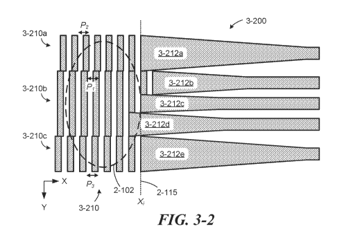
the one or more
beams into a plurality of receiving regions connected to the plurality of
optical waveguides;
monitoring a first amount of radiation received from a first waveguide of the
plurality of optical
waveguides; and determining whether the one or more beams move toward or away
from an
inlet of the first waveguide in a direction perpendicular to lines of the
grating based, at least in
part, upon the monitored amount of radiation.
[0007] Some embodiments relate to a method of making an integrated device. The
method
may comprise acts of forming a plurality of waveguides on a substrate; forming
a grating on the
substrate that spans inlets to the plurality of waveguides; locating a first
inlet to a first
waveguide of the plurality of waveguides along a reference line for the
grating; and offsetting a
second inlet to a second waveguide of the plurality of waveguides by a first
distance from the
reference line, wherein the first distance is in a first direction
perpendicular to lines of the
grating.
[0008] Some embodiments relate to an integrated device comprising a grating
disposed on a
substrate and arranged to couple radiation incident on the grating into a
plurality of optical
waveguides disposed on the substrate; a first inlet to a first waveguide of
the plurality of optical
waveguides; and a second inlet to a second waveguide of the plurality of
optical waveguides,
wherein a first portion of the grating located adjacent to the first inlet has
a different periodicity
than a second portion of the grating located adjacent to the second inlet.
[0009] Some embodiments relate to a method of coupling radiation into a
plurality of optical
waveguides formed on a substrate, the method comprising acts of receiving one
or more beams
of radiation on a grating; coupling radiation from the one or more beams into
a plurality of
optical waveguides; monitoring a signal received from a first waveguide of the
plurality of
optical waveguides; and determining whether an incident pitch angle of the one
or more beams
on the grating changes in a direction perpendicular to lines of the grating
based, at least in part,
upon the signal monitored from the first waveguide.
[0010] Some embodiments relate to a method of making an integrated device. The
method
2
CA 03142922 2021-12-07
WO 2020/251690 PCT/US2020/030345
may comprise acts of forming a plurality of waveguides on a substrate, each
waveguide having
an inlet adjacent to a grating; and forming the grating on the substrate to
span the inlets to the
plurality of waveguides, wherein a first portion of the grating located
adjacent to a first inlet to a
first waveguide of the plurality of waveguides has a different periodicity
than a second portion
of the grating located adjacent to a second inlet to a second waveguide of the
plurality of
waveguides.
[0011] The foregoing and other aspects, implementations, acts,
functionalities, features and,
embodiments of the present teachings can be more fully understood from the
following
description in conjunction with the accompanying drawings.
BRIEF DESCRIPTION OF THE DRAWINGS
[0012] The skilled artisan will understand that the figures, described herein,
are for illustration
purposes only. It is to be understood that in some instances various aspects
of the invention may
be shown exaggerated or enlarged to facilitate an understanding of the
invention. In the
drawings, like reference characters generally refer to like features,
functionally similar and/or
structurally similar elements throughout the various figures. The drawings are
not necessarily to
scale, emphasis instead being placed upon illustrating the principles of the
teachings. The
drawings are not intended to limit the scope of the present teachings in any
way.
[0013] FIG. 1-1 is a perspective view depicting optical pulses incident on a
grating coupler,
according to some embodiments.
[0014] FIG. 1-2 is a plan view depicting an example of a grating coupler
arranged to couple
optical radiation into a plurality of waveguides, according to some
embodiments.
[0015] FIG. 1-3 is an elevation view of a grating coupler, according to some
embodiments.
[0016] FIG. 2-1 is a plan view of an example grating coupler with improved
sensitivity to
beam alignment, according to some embodiments.
[0017] FIG. 2-2 is a plan view of an example grating coupler with improved
sensitivity to
beam alignment, according to some embodiments.
[0018] FIG. 2-3 is a plan view of an example grating coupler with improved
sensitivity to
beam alignment for a plurality of incident beams, according to some
embodiments.
[0019] FIG. 2-4 depicts signal characteristics for signals received from
receiving regions of a
grating coupler having improved sensitivity to beam alignment, according to
some
embodiments.
[0020] FIG. 3-1 is a plan view of an example grating coupler with improved
sensitivity to
beam alignment, according to some embodiments.
[0021] FIG. 3-2 is a plan view of an example grating coupler with improved
sensitivity to
3
CA 03142922 2021-12-07
WO 2020/251690 PCT/US2020/030345
beam alignment, according to some embodiments.
[0022] FIG. 3-3 depicts signal characteristics for signals received from
receiving regions of a
grating coupler having improved sensitivity to beam alignment, according to
some
embodiments.
[0023] FIG. 3-4 depicts an example of a receiving region and corresponding
grating portion,
according to some embodiments.
[0024] FIG. 3-5 is a flow chart depiction of a method for aligning and
maintaining alignment
of an incident beam on a grating coupler, according to some embodiments.
[0025] FIG. 4 depicts a cutaway perspective view of a portion of an integrated
device,
according to some embodiments.
[0026] FIG. 5-1A is a block diagram depiction of an analytical instrument that
includes a
compact mode-locked laser module, according to some embodiments.
[0027] FIG. 5-1B depicts a compact mode-locked laser module incorporated into
an
analytical instrument, according to some embodiments.
[0028] FIG. 5-2 depicts a train of optical pulses, according to some
embodiments.
[0029] FIG. 5-3 depicts an example of parallel reaction chambers that can be
excited optically
by a pulsed laser via one or more waveguides and further shows corresponding
detectors for
each chamber, according to some embodiments.
[0030] FIG. 5-4 illustrates optical excitation of a reaction chamber from a
waveguide,
according to some embodiments.
[0031] FIG. 5-5 depicts further details of an integrated reaction chamber,
optical waveguide,
and time-binning photodetector, according to some embodiments.
[0032] FIG. 5-6 depicts an example of a biological reaction that can occur
within a reaction
chamber, according to some embodiments.
[0033] FIG. 5-7 depicts emission probability curves for two different
fluorophores having
different decay characteristics.
[0034] FIG. 5-8 depicts time-binning detection of fluorescent emission,
according to some
embodiments.
[0035] FIG. 5-9 depicts a time-binning photodetector, according to some
embodiments.
[0036] FIG. 5-10A depicts pulsed excitation and time-binned detection of
fluorescent
emission from a reaction chamber, according to some embodiments.
[0037] FIG. 5-10B depicts a histogram of accumulated fluorescent photon counts
in various
time bins after repeated pulsed excitation of an analyte, according to some
embodiments.
[0038] FIG. 5-11A ¨ 5-11D depict different histograms that may correspond to
the four
nucleotides (T, A, C, G) or nucleotide analogs, according to some embodiments.
4
CA 03142922 2021-12-07
WO 2020/251690 PCT/US2020/030345
[0039] The features and advantages of the present invention will become more
apparent from
the detailed description set forth below when taken in conjunction with the
drawings. When
describing embodiments in reference to the drawings, directional references
("above," "below,"
"top," "bottom," "left," "right," "horizontal," "vertical," etc.) may be used.
Such references are
intended merely as an aid to the reader viewing the drawings in a normal
orientation. These
directional references are not intended to describe a preferred or only
orientation of features of
an embodied device. A device may be embodied using other orientations.
DETAILED DESCRIPTION
[0040] I. Grating Couplers
[0041] Grating couplers are useful integrated optical devices for coupling
optical radiation
from an external optical beam into integrated optical waveguides located on a
substrate. For
explanation purposes, FIG. 1-1 illustrates an example of a grating coupler 1-
100 that is
integrated on a substrate 1-105. A grating coupler 1-100 can comprise an
optical grating 1-110
and a receiving region 1-112 of an optical waveguide having an inlet 1-111. In
the illustrated
example, the grating 1-110 is located adjacent to the inlet 1-111, and the
grating coupler 1-100 is
configured to redirect and couple incident optical radiation (depicted as a
beam of optical pulses
1-122 travelling along an optical axis 1-101 of the beam) into the receiving
region 1-112 of a
waveguide via the inlet 1-111. The receiving region 1-112 may connect to one
or more
waveguides downstream from the inlet 1-111, as depicted in FIG. 1-2. For
directional reference
in the illustration of FIG. 1-1, a coordinate axis is chosen such that the x
and y directions are
parallel to a top surface of the substrate 1-105 on which the grating coupler
is formed. However,
the invention is not limited to the illustrated orientation of a Cartesian
coordinate reference
frame. Other reference frames (polar, spherical) and other orientations may be
used to describe
the invention.
[0042] When describing a component as being "on" or "over" a substrate or
layer, the
component may be directly on the substrate or layer, or there may be one or
more intervening
layers of material and/or one or more intervening components between the
component and the
substrate or layer. The phrase "directly on" is used to indicate that a
component is in direct
physical contact with an immediately adjacent substrate or layer.
[0043] FIG. 1-2 is a plan view of an example grating coupler 1-100 and
portions of
waveguides 1-213a, 1-213b formed on a substrate 1-105. The grating coupler 1-
100 can connect
to and couple radiation into a first waveguide 1-213, which can connect to two
or more
waveguides 1-213a, 1-213b. Any of the waveguide sections may be single
transverse mode or
multimode waveguides. Any of the waveguide sections can comprise a waveguide
core formed
CA 03142922 2021-12-07
WO 2020/251690 PCT/US2020/030345
by a first dielectric material having a first index of refraction and one or
more cladding layers
surrounding, or partly surrounding, the core. Values of indices of refraction
for the one or more
cladding layers can be less than the index of refraction for the waveguide
core.
[0044] A power divider 1-225 may divide power received from the first
waveguide 1-213 into
the two illustrated waveguides 1-213a, 1-213b, according to some embodiments.
In some
implementations, power from a first waveguide 1-213 may be divided into more
than two
waveguides. In some cases, a power divider may not be used and only a single
waveguide 1-213
may extend from the grating coupler 1-100. In some cases, waveguides 1-213a, 1-
213b may
connect to additional power dividers so that optical power in the waveguides
can be further
distributed to a plurality of waveguides.
[0045] Some examples of power dividers 1-225 include waveguide couplers or
waveguide
splitters, in which a propagating mode in a first waveguide couples
evanescently to one or more
propagating modes in one or more adjacent waveguides. Other examples of power
dividers 1-
225 include interferometric splitters, such as Mach-Zehnder interferometers
and multi-mode
interference couplers. Regardless of the type of power divider 1-225 and
number of downstream
waveguides, power from the first waveguide 1-213 can be divided equally or
unequally among
the downstream waveguides by selecting a suitable design and splitting ratio
of the power
divider 1-225.
[0046] FIG. 1-3 depicts an elevation view that roughly corresponds to the
structure shown in
FIG. 1-1, according to one embodiment. An optical grating 1-110 can be
patterned as lines 1-
116 in a first material that has a higher (or lower in some cases) index of
refraction than an
adjacent material 1-310 adjacent to the grating lines. (The adjacent material
1-310 is not shown
in FIG. 1-1.) In some embodiments, an optical grating 1-110 is embedded in one
or more
surrounding materials. For example, instead of a single adjacent material 1-
310 surrounding the
grating 1-110, the grating may be formed between two or more layers of
different material.
Lines (or teeth) 1-116 of the grating 1-110 can be formed from a single layer
of material (as
depicted in FIG. 1-1), or may comprise two or more layers of material (as
depicted in FIG. 1-3).
For example, a second material 1-312 may be deposited over a first material 1-
311 and patterned
when forming the lines 1-116. Addition of one or more second material layers
may improve the
diffraction efficiency of the grating 1-110. Materials that may be used to
form the grating lines
1-116 include, but are not limited to, dielectrics (oxides, nitrides),
semiconductors, metals, and
combinations of these materials when two or more layers are used. Such example
materials
include silicon oxide, tantalum oxide, aluminum oxide, silicon nitride,
nitrogen-rich silicon
nitride (e.g., having more nitride than a stoichiometric ratio for Si3N4),
silicon, silicon-
germanium, germanium, aluminum, tungsten, and polymeric materials. In one
example
6
CA 03142922 2021-12-07
WO 2020/251690 PCT/US2020/030345
embodiment, a grating 1-110 can be formed primarily from nitrogen-rich silicon
nitride and the
adjacent material 1-310 surrounding the grating can comprise silicon oxide.
[0047] One or more adjacent materials 1-310 surrounding the optical grating 1-
110 can be
optically transparent to the optical radiation that is being coupled into the
receiving region 1-112
by the optical grating 1-110. Preferably, the one or more adjacent materials 1-
310 exhibits low
optical loss to the optical radiation that is being coupled into the
waveguide. Materials that may
be used for the one or more adjacent materials 1-310 include, but are not
limited to, oxides,
nitrides, and polymers as described above.
[0048] According to some embodiments, an optical grating 1-110 can have a
periodicity P
between 200 nm and 800 nm. In other embodiments, the grating 1-110 may have a
periodicity P
less than 200 nm or greater than 800 nm. A duty cycle of the grating (ratio of
width of a grating
line 1-116 in the x direction to the periodicity P can be between 20 % and 80
%. A thickness tg
of the grating lines 1-116 can be between 20 nm and 500 nm, according to some
embodiments.
A width wg of the grating teeth 1-116 associated with coupling into a single
inlet 1-111 can be
between 50 nm and 500 nm. According to some embodiments, a last line 1-116 of
the grating 1-
110 adjacent to the inlet 1-111 may be spaced from the inlet 1-111 by a
distance that is
equivalent to a space between the grating lines 1-116 (as depicted in FIG. 1-
1). In some cases, a
last line 1-116 of the grating 1-110 may be spaced from the inlet 1-111 by a
distance that is an
integer number of spaces between the grating lines 1-116 or a non-integer
number of spaces
between the grating lines 1-116.
[0049] A receiving region 1-112 and an optical waveguide 1-213 can be
patterned in a first
material that has a higher index of refraction than an adjacent material 1-310
to the receiving
region 1-112 and/or waveguide 1-213. In some embodiments, the receiving region
1-112 and
optical waveguide 1-213 can be embedded in one or more surrounding materials.
The receiving
region, waveguide, and one or more surrounding materials can be optically
transparent to the
radiation transported by the waveguide. Preferably, the receiving region 1-
112, waveguide 1-
213, and one or more adjacent materials 1-310 exhibit low optical loss to the
optical radiation
transported by the waveguide (e.g., less than 1 dB/cm). Materials that may be
used for the
receiving region 1-112, waveguide 1-213, downstream waveguides 1-213a, 1-213b,
and the one
or more second materials 1-310 include, but are not limited to, oxides and
nitrides as described
above. As an example, the waveguide 1-213, receiving region 1-112, and
downstream
waveguides 1-213a, 1-213b can be formed from silicon nitride (or a nitrogen-
rich silicon nitride)
and the one or more adjacent materials 1-310 can be formed from silicon oxide.
[0050] According to some embodiments, a receiving region 1-112 may be tapered,
as
illustrated in the example of FIG. 1-1. Along the tapered region, a width wt
of the waveguide
7
CA 03142922 2021-12-07
WO 2020/251690 PCT/US2020/030345
core in the receiving region may decrease in size in an x direction, moving
away from the inlet
1-111, until it matches a width w of a core in a uniform portion of the
waveguide 1-213 at a
downstream location, as depicted in FIG. 1-2. In other embodiments, a width wt
of the
waveguide core in the tapered region 1-112 may increase in size in an x
direction, moving away
from the inlet 1-111, until it matches a width w of a uniform portion of the
core of the
waveguide 1-213. Additionally or alternatively, a thickness t,, of a core in
the receiving region
1-112 can be tapered, changing in size until it matches a thickness of a core
of the connected
waveguide 1-213. Tapering the width and/or thickness of the core in the
receiving region 1-112
can improve coupling efficiency of the optical radiation into the receiving
region and
downstream waveguide, e.g., when a transverse size (mode profile) of an
incident beam is
significantly different than the size of an optical mode (e.g., fundamental
mode size) supported
by the waveguide 1-213.
[0051] According to some embodiments, a width w of a core in a uniform portion
of a
waveguide 1-213 can be between 200 nm and 800 nm. A thickness tw of a core in
the uniform
portion of a waveguide 1-213 can be between 20 nm and 500 nm. In some
implementations, a
width and thickness of a waveguide core is selected such that the waveguide 1-
213 supports only
a single transverse optical mode (a fundamental optical mode) within the
waveguide. In some
cases, a waveguide 1-113 may support more than one transverse optical mode. A
width wt of a
core in the tapered receiving region 1-112 may be smaller than 200 nm at the
inlet 1-111 in some
cases, or larger than 800 nm at the inlet in other cases. In some
implementations, the receiving
region may not be tapered. A thickness tw of a core at the inlet of the
receiving region 1-112 can
be between 20 nm and 500 nm.
[0052] A grating 1-110, receiving region 1-112, and waveguide 1-213 can be
fabricated using
planar microfabrication techniques, such as those described in U.S. Patent
Application No.
15/844,403 filed December 15, 2017 and title "Optical Coupler and Waveguide
System," which
application is incorporated herein by reference in its entirety. Such
microfabrication techniques
can include steps of patterning gratings and waveguides in resist using
photomasks and
photolithography techniques, and etching patterns of the gratings and
waveguides in oxide
and/or nitride layers using etching processes such as anisotropic reactive ion
etching. Such
microfabrication techniques can also include steps of depositing resists and
layers used to form
the grating coupler, and removing residual resists and portions of layers.
[0053] In operation, a grating coupler 1-100 can diffract incident optical
radiation into one or
more different directions away from the path of the incident beam (which
proceeds along an
optical axis 1-101). By designing the grating coupler carefully (e.g.,
choosing an appropriate
pitch P of the grating 1-110 for an operating, characteristic wavelength) and
orienting the
8
CA 03142922 2021-12-07
WO 2020/251690 PCT/US2020/030345
incident beam correctly, a majority of the incident optical radiation can be
diffracted toward the
inlet 1-111 from the grating 1-100 and essentially coaxial with the receiving
region 1-112.
Thereby, a majority of incident radiation can couple into the receiving region
1-112 and
downstream waveguide 1-213. The orientation of the incident beam (shown as
pulses 1-122 in
the example of FIG. 1-1) can be described by the beam's location and incident
angles. For
example, the beam's location on the grating 1-110 may be describes as a
position (in x and y
directions) of a center (e.g., optical axis 1-101) of the beam with respect to
a center of the
grating 1-110 or a center of the inlet 1-111 in some cases. The beam's
incident angles may be
described by a first incidence angle or pitch angle a (e.g., measured from the
z axis toward the x
direction, rotating about the y axis), and a second incidence angle or tilt
angle ç (e.g., measured
from the z axis toward the y direction, rotating about the x axis). Changes in
the beam's position
on the grating 1-110, pitch angle a, and tilt angle ç can change the coupling
efficiency of the
incident beam into the receiving region 1-112 and downstream waveguide 1-213.
[0054] Features, materials, and dimensions described above for the grating
coupler
embodiments of FIG. 1-1, FIG. 1-2, and FIG. 1-3 can be implemented in the
grating couplers
described in the following embodiments that couple directly from a grating 1-
110 to more than
one receiving region.
[0055] The inventors have recognized and appreciated that once an incident
beam of optical
pulses 1-122 (or continuous wave incident beam) is aligned to the grating
coupler 1-100 for a
highest coupling efficiency, there can be ambiguities or uncertainties in
knowing how a beam's
orientation has changed when reductions in power coupled into a receiving
region 1-112 or
downstream waveguides are detected. For example, when oriented for highest
coupling
efficiency with regard to position of the incident beam on the grating 1-110,
motion of the beam
toward the inlet 1-111 or away from the inlet 1-111 produces a very similar
characteristic
reduction in coupling efficiency. Therefore, by detecting a reduction in power
in a downstream
waveguide, one cannot determine readily whether the incident beam has moved
toward or away
from the inlet 1-111. Accordingly, automated correction of beam position to
maintain a high
coupling efficiency is complicated by the ambiguity in x-directed motion of
the beam.
[0056] A similar result occurs for changes in the pitch angle a. For example,
after obtaining a
highest coupling efficiency with regard to pitch angle, an increase or
decrease in pitch angle
produces a essentially a same reduction in coupling efficiency. Therefore,
automated correction
of beam position to maintain a high coupling efficiency is further complicated
by the ambiguity
in a -directed motion of the beam.
9
CA 03142922 2021-12-07
WO 2020/251690 PCT/US2020/030345
[0057] FIG. 2-1 depicts an embodiment of a grating coupler 2-100 having
improved beam-
alignment sensitivity in which a direction of movement of the incident beam 2-
102 in an x
direction (causing a reduction in coupling efficiency) can be disambiguated.
The illustration
shows a plan view of the grating coupler. In the illustrated embodiment, the
grating coupler 2-
100 comprises five receiving regions 2-112a ¨ 2-112e having five inlets 2-111a
¨ 2-111e, some
of which are offset with respect to other inlets in the x direction or in a
direction perpendicular or
essentially perpendicular to lines 2-116 of the grating. In some
implementations, there can be
fewer or more than five receiving regions. For some applications, there can be
tens or over a
hundred receiving regions and inlets in a grating coupler 2-100. To simplify
the illustration,
only the grating lines and receiving regions of the waveguides are shown. The
grating lines 2-
116 and receiving regions 2-112a ¨ 2-112e of the waveguides can be formed on a
substrate 1-
105 along with surrounding materials, as described above in connection with
FIG. 1-1 through
FIG. 1-3.
[0058] By using multiple inlets 2-111a ¨ 2-111e, the grating coupler 2-100 can
couple
radiation from a high power beam 2-102 directly into multiple waveguides. (An
example
transverse beam profile, such as 1/e2 width(s), is indicated as a dashed
ellipse.) Coupling
directly into multiple waveguides can be advantageous to avoid damaging the
optical
waveguides and to avoid undesirable nonlinear optical behavior that can occur
at higher powers.
Further, the transverse widths Wt of the inlets 2-111a ¨ 2-111e in the y
direction can be sized to
obtain a desired power ratio among the receiving regions 2-112a ¨ 2-112e. For
example, the
outer inlets 2-111a, 2-111e can be wider than the center inlet 2-111c, such
that each receiving
region 2-112a, 2-112c, and 2-112e couples approximately a same amount of
optical power from
the incident beam. In some embodiments, all receiving regions may couple
approximately a
same amount of optical power from the incident beam, so that each waveguide
downstream of a
receiving region carries approximately a same amount of optical power. Other
power coupling
ratios may be implemented in other embodiments by selecting appropriate widths
of the inlets 2-
111a ¨ 2-111e and receiving regions 2-112a ¨ 2-112e.
[0059] According to some embodiments, one or more of the inlets 2-111a ¨ 2-
111e may be
located essentially along a same reference line 2-115, which may be straight
or curved. In some
cases, as depicted in the illustrated example of FIG. 2-1, a majority of the
inlets 2-111a, 2-111c,
2-111e are located along a same reference line 2-115 (depicted as a dotted
line at x = Xi).
Although the reference line is shown as being straight in the illustration, in
some
implementations the reference line 2-115 may be curved (e.g., to accommodate a
curvature of
the shape of the incident beam 2-102). A reference line 2-115 can correspond
to locations where
two or more inlets of receiving regions would be located to provide highest
coupling efficiencies
CA 03142922 2021-12-07
WO 2020/251690 PCT/US2020/030345
into the two or more receiving regions when an incident beam is positioned on
a grating for
highest coupling efficiency into one of the two or more receiving regions. For
a grating coupler
2-100 having improved x-direction sensitivity at least one inlet is located
away from the
reference line 2-115 in an x direction by an amountl&l. In some embodiments,
two or more
inlets are located away from the reference line 2-115 in an x direction by an
amountl&lor by
two different amounts. In some cases, it is possible to have a majority of the
inlets located away
from the reference line 2-115 in an x direction by an amountl&lor by a
plurality of different
amounts. In such cases, a reference line 2-115 may align with as few as one
inlet (e.g., an inlet
located at an average x location among all inlets).
[0060] An amount by which one or more inlets 2-111b, 2-111d can be offset from
a reference
line 2-115 can be between 0.5 micron and 10 microns, or approximately these
end values
according to some embodiments, and for a wavelength of the incident beam
between 400 nm
and 800 nm or approximately these end values. The offset inlets 2-111b, 2-111d
and receiving
regions 2-112b, 2-112d can couple less power than they would if they were
located on the
reference line 2-115. In some embodiments, the widths of the offset inlets and
receiving regions
may be sized to couple a desired power ratio among all inlets and receiving
regions (e.g., a same
amount of power into each inlet and receiving region).
[0061] Disambiguation of beam motion can be sensed by monitoring power in a
waveguide
connected to an offset inlet (e.g., inlet 2-112d). For example and referring
again to FIG. 2-1, an
initial beam alignment can optimize power coupled into one or more inlets and
receiving regions
lying along a reference line 2-115 (such as inlet 2-111c and receiving region
2-112c). For
optimization of coupling efficiency, power or intensity can be monitored from
waveguide(s)
connected to the one or more inlets and receiving regions lying along the
reference line 2-115.
In some cases, monitoring can be done at one or more sites on a chip to which
a waveguide
delivers power. For example, a site on a chip may include a photodetector that
can sense an
amount of intensity of radiation in a waveguide. After optimization of
coupling efficiency,
power or intensity monitored in one or more offset inlets and receiving
regions can indicate
which direction (in x) an incident beam moves. For example, if power is
monitored in a
waveguide connected to receiving region 2-112d, an increase in power would
indicate that the
incident beam 2-102 has moved in the ¨x (upstream) direction. A decrease in
power would
indicate that the incident beam 2-102 has moved in the +x (downstream)
direction. Although
examples described herein refer to power of the incident beam, intensity may
be monitored
alternatively or additionally.
[0062] For the same grating coupler 2-100, power monitored in a waveguide
connected to
receiving region 2-112b would show an opposite behavior to that of power
monitored in a
11
CA 03142922 2021-12-07
WO 2020/251690 PCT/US2020/030345
waveguide connected to receiving region 2-112d. Movement of the incident beam
2-102 in the
¨x direction would result in a decrease of power coupled into the receiving
region 2-112b.
Movement of the incident beam 2-102 in the +x direction would result in an
increase of power
coupled into the receiving region 2-112b. Differencing power signals from two
waveguides
connected to the two receiving regions 2-112b, 2-112d can increase the
sensitivity for detecting
motion of the input beam 2-102.
[0063] FIG. 2-2 depicts another embodiment of a grating coupler 2-200 having
improved
beam-alignment sensitivity. The grating coupler 2-200 may be nearly the same
as the grating
coupler 2-100 of FIG. 2-1, except that the inlets and receiving regions 2-112a
¨ 2-112e are
spatially separated in the y direction rather than being abutted and in
contact at their edges. The
grating 2-210 may comprise separated portions 2-210a ¨ 2-210e, as illustrated
in FIG. 2-2, or
may be formed with continuous lines 2-116 as shown in FIG. 2-1. Separating the
inlets 2-111a
¨ 2-111e and receiving regions 2-112a ¨ 2-112e in the y direction may result
in a reduced
coupling efficiency, but may improve optical mode profiles in the receiving
regions by reducing
effects of discontinuities in the immediately abutted inlet faces. The grating
2-210 and receiving
regions 2-112a ¨ 2-112e can be formed on a substrate 1-105 along with
surrounding materials,
as described above in connection with FIG. 1-1 through FIG. 1-3.
[0064] In some applications, it may be desirable to couple a plurality of
incident beams 2-330
into a plurality of integrated waveguides. FIG. 2-3 illustrates another
embodiment of a grating
coupler 2-300 having improved beam-alignment sensitivity for such
applications. The grating
coupler 2-300 can comprise a grating 2-310 and a plurality of receiving
regions 2-312a ¨ 2-312d
adjacent to the grating 2-310. The grating may comprise separated portions 2-
310a ¨ 2-310d, as
illustrated, or may be formed like the grating in FIG. 2-1 having continuous
lines 2-116. The
receiving regions 2-312a ¨ 2-312d may be separated in a y direction as
illustrated, or may be
abutted immediately adjacent to each other. At least one of the receiving
regions and inlets may
be offset in the x direction from a reference line 2-115. According to some
implementations, the
widths of the receiving regions and inlets may be approximately the same. In
some
embodiments, widths of receiving regions and inlets for the offset gratings
may be larger than
widths of receiving regions and inlets for inlets lying on the reference line
2-115 (e.g., in order
to obtain a same amount of power in each receiving region).
[0065] Provided the plurality of incident beams 2-330 move together as a unit,
rather than
independently, motion of the plurality of incident beams 2-330 in the x
direction will produce
the same changes in power coupled into the offset receiving regions as
described above in
connection with FIG. 2-1. For example, motion of the incident beams 2-330 in
the +x direction
can be detected as an increase in power for a waveguide connected to receiving
region 2-312b
12
CA 03142922 2021-12-07
WO 2020/251690 PCT/US2020/030345
and a decrease in power for a waveguide connected to receiving region 2-312c.
Also, motion of
the incident beams 2-330 in the ¨x direction can be detected as a decrease in
power for a
waveguide connected to receiving region 2-312b and an increase in power for a
waveguide
connected to receiving region 2-312c. The grating 2-310 and receiving regions
2-312a ¨ 2-312e
can be formed on a substrate 1-105 along with surrounding materials, as
described above in
connection with FIG. 1-1 through FIG. 1-3.
[0066] FIG. 2-4 plots simulation results for a grating coupler having improved
sensitivity to
changes in the x position of an incident beam, such as the coupler illustrated
in FIG. 2-1. A first
curve 2-402 illustrates a change in signal S, received from a receiving region
2-112c having an
inlet lying on a reference line 2-115. Highest coupling efficiency into the
receiving region 2-
112c is obtained for an incident beam positioned at a reference x position
(arbitrarily set to
0 microns). As can be seen from the first curve 2-402, the signal level
changes similarly for an
increase or decrease in beam position along the x direction. Although there is
an asymmetry in
the curve, the difference can be small and difficult or impossible to reliably
discern in an
implemented automated system. For example, each signal value between -20
microns and 20
microns does not uniquely identify a beam position. A second curve 2-404
illustrates a change
in a difference signal Sd - Sb received from two receiving regions that are
offset from the
reference line 2-115, as depicted in FIG. 2-1. The difference signal shows a
continuous increase
for changes in beam location from x -7 microns to x +7, and can clearly
distinguish motion
of the beam in the ¨x direction from motion of the beam in the +x direction.
Nonlinearity in the
curve can be calibrated and compensated for electronically. For this
simulation, the two
receiving regions were offset by +5 microns and -5 microns, though the
invention is not limited
to only these offset values. Smaller or larger offsets may be used in some
embodiments.
[0067] Another embodiment of a grating coupler 3-100 having improved beam-
alignment
sensitivity is illustrated in FIG. 3-1. The illustrated example can
disambiguate changes in pitch
angle a (illustrated in FIG. 1-1) of an incident beam 2-102. For such
embodiments, the grating
coupler 3-100 can comprise a grating 3-110 having a plurality of portions 3-
110a ¨ 3-110e, at
least two of which have different or offset grating periodicities (e.g., Pi,
P2). In some
implementations, the inlets of receiving regions 3-112a ¨ 3-112e may lie along
a common
reference line 2-115, which may be straight or curved as described above. The
grating portions
3-110a ¨ 3-110e and receiving regions 3-112a ¨ 3-112e may immediately abut
each other in the
y direction, as illustrated, or may be separated from each other (like those
depicted in FIG. 2-2).
In some embodiments, the grating portions 3-110a ¨ 3-110e and receiving
regions 3-112a ¨ 3-
112e may be separated and sized as depicted in FIG. 2-3 for coupling a
plurality of incident
beams into a plurality of waveguides.
13
CA 03142922 2021-12-07
WO 2020/251690 PCT/US2020/030345
[0068] One or more of the grating portions 3-110a, 3-110c, 3-110e may have a
same grating
periodicity Pi which may be a reference periodicity. In some cases, a majority
of the grating
portions 3-110a, 3-110c, 3-110e may have a same reference grating periodicity
Pi. The
reference periodicity may be one that provides a highest coupling efficiency
into each of the
corresponding receiving regions (e.g., receiving regions 3-112a, 3-112c, 3-
112e) when an
incident beam 2-102 is oriented for a highest coupling efficiency into one of
the corresponding
receiving regions. At least one of the grating portions 3-110b can have an
offset periodicity P2
that differs from the reference periodicity Pi. An offset periodicity may
result in reduced
coupling efficiency into the corresponding receiving region 3-112b. In some
cases, there may be
one or more additional grating portions 3-110d having one or more additional
offset periodicities
P3. The grating 3-110 and receiving regions 3-112a¨ 3-112e can be formed on a
substrate 1-
105 along with surrounding materials, as described above in connection with
FIG. 1-1 through
FIG. 1-3.
[0069] For a grating portion 3-110a having a reference periodicity Pi,
diffraction of a portion
of the incident beam can be essentially in the y direction, e.g., directly
into the corresponding
inlet and essentially coaxial with a core of the receiving region. A change in
pitch of the
incident beam in the +a direction would produce essentially the same reduction
in power
behavior as a change in pitch in the ¨a direction (referring again to FIG. 1-
1.) For a grating
portion 3-110b having a periodicity P2 that is less than Pi, diffraction of a
portion of the incident
beam can be mainly in the y direction but also partly in the ¨z direction (out
of the paper). This
can result in reduced coupling efficiency into the receiving region 3-112b.
However, a change
in pitch of the incident beam in the +a direction would decrease power coupled
into the
receiving region 3-112b, whereas a change in pitch of the incident beam in the
¨a direction
would increase power coupled into the receiving region 3-112b. Monitoring
power or intensity
from a waveguide coupled to the receiving region 3-112b can then disambiguate
changes in
pitch of the incident beam 2-102 in the a directions.
[0070] An opposite behavior from that of grating portion 3-110b can be
obtained for a grating
portion 3-110d having a periodicity P3 that is greater than Pi. Where the
periodicity P3 is
greater than the reference periodicity Pi, diffraction of a portion of the
incident beam can be
mainly in the y direction but also partly in the +z direction (into the plane
of the figure). A
change in pitch of the incident beam in the +a direction would increase power
coupled into the
receiving region 3-112d, whereas a change in pitch of the incident beam in the
¨a direction
would decrease power coupled into the receiving region 3-112d. Differencing
signals received
14
CA 03142922 2021-12-07
WO 2020/251690 PCT/US2020/030345
from both receiving regions 3-112b, 3-112d can increase detection sensitivity
for changes of
incident beam orientation in the a directions.
[0071] According to some embodiments, the amount of offset in grating
periodicity from the
reference periodicity Pi can be between 0.1% and 1% of the reference
periodicity Pi. For some
visible optical configurations, the change in periodicity of an offset grating
can be between 0.5
nm and 4 nm, or between approximately 0.5 nm and approximately 4 nm.
[0072] FIG. 3-2 depicts an example of a grating coupler 3-200 that combines
the aspects of
offset receiving regions 3-212b, 3-212d and offset grating periodicities P2,
P3. The grating
coupler 3-200 can include a grating 3-210 comprising a grating portion 3-210b
that has a
reference periodicity Pi and one or more additional portions 3-210a, 3-210c
with one or more
offset periodicities P2, P3. The grating coupler 3-200 may further include one
or more receiving
regions 3-212a, 3-212c, 3-212e having inlets located along a reference line 2-
115 and one or
more receiving regions 3-212b, 3-212d with inlets that are offset in an x
direction from the
reference line 2-115. For the illustrated example, power changes detected from
waveguides
connected to the receiving regions 3-212b and/or 3-212d can unambiguously
indicate motion of
the incident beam location on the grating 3-210 in the +x or ¨x direction.
Power changes
detected from waveguides connected to the receiving regions 3-212a, 3-212e can
unambiguously
indicate motion of the incident beam location on the grating 3-210 in the +a
or ¨a direction.
[0073] FIG. 3-3 plots simulation results for a grating coupler having improved
sensitivity to
changes in the pitch angle a of an incident beam, such as the coupler
illustrated in FIG. 3-1. A
first curve 3-302 illustrates a change in signal S, received from a receiving
region 3-112c that is
adjacent to a grating having a reference periodicity Pi. For the chosen
grating design and
characteristic wavelength, a highest coupling efficiency into a receiving
region adjacent to a
grating portion having the reference periodicity is obtained for an incident
pitch angle of ¨4.0
degrees. As can be seen from the first curve 3-302, the signal level changes
essentially
identically for an increase or decrease in incident pitch angle of the beam
from an aligned
position at -4.0 degrees. Each signal level does not uniquely identify an
incident angle of the
beam. A second curve 3-304 illustrates a change in a difference signal Sd - Sb
received from two
receiving regions that are adjacent to two grating portions having offset
periodicities (P2 < Pi, P3
> Pi). The difference signal is essentially linear over the range of incident
angles and can
clearly indicate the direction of change in pitch angle. For this simulation,
the difference in
offset grating periodicities were +1 nm and -1 nm from the periodicity Pi of
the reference
grating, though offsets in grating periodicities are not limited to only these
values. Smaller or
larger offsets in grating periodicity may be used.
CA 03142922 2021-12-07
WO 2020/251690 PCT/US2020/030345
[0074] Although the grating lines and inlets of receiving regions in the
embodiments
illustrated in FIG. 2-1 through FIG. 3-2 are depicted as straight, in some
implementations the
grating lines and inlets may be curved in any of the embodiments. FIG. 3-4
illustrates an
example in which a grating 3-410 adjacent to a receiving region 3-412 has
curved lines 3-416.
Additionally the inlet 3-411 of the receiving region 3-412 may have a curved
surface. Curved
grating lines 3-416 and/or a curved inlet 3-411 may improve coupling
efficiency into the
receiving region 3-412. In some cases, curved grating lines 3-416 and/or a
curved inlet 3-411
may additionally or alternatively improve optical mode profile in the
receiving region 3-412.
[0075] FIG. 3-5 is a flow chart illustrating an example method 3-500 for
aligning and
maintaining alignment of an incident beam on a grating coupler of the present
embodiments.
Some or all of the acts of the method may be automated (e.g., by using
automated beam-steering
and positioning instruments). A method 3-500 may include acts of first
aligning (act 3-510) an
incident beam 2-102 on a grating 2-110 of a grating coupler 2-100. An aligned
position may be
an orientation that provides a highest, or approximately highest, coupling
efficiency into a
reference receiving region (e.g., a receiving region having an inlet 2-111
lying on a reference
line 2-115 and/or a receiving region having an inlet for a corresponding
reference grating
periodicity Pi). After an aligned orientation is obtained, the beam
orientation may be scanned in
x and/or a directions to calibrate (act 3-520) sensors and signal levels over
a set range of
misaligned orientations. For each independent degree of freedom, an alignment
signal level can
be monitored (act 3-530). An alignment signal level may be monitored by one or
more sensors
integrated on a substrate on which the waveguides and grating coupler are
formed. In some
implementations, the sensors may be located in pixels of an analytic
instrument, which is
described in further detail below. An automated system may test for a signal
level increase (act
3-540) or decrease (act 3-550). If a signal level increase is detected (e.g.,
resulting from beam
motion in the +x direction), the automated system may move the beam in the ¨x
direction (act 3-
545) until the signal level is restored to essentially an aligned signal level
and resume monitoring
the signal (act 3-530). An aligned signal level may be a voltage level V,
determined during
calibration (act 3-520) of the automated alignment system, and the system may
be configured to
accept a range of values within a few percent of V, as indicating alignment.
If a signal level
decrease is detected (e.g., resulting from beam motion in the ¨x direction),
the automated system
may move the beam in the +x direction (act 3-555) until the signal level is
restored to an aligned
level and resume monitoring the signal (act 3-530). According to some
embodiments, motion of
the beam may be implemented using a galvanometer or stepper motor to move an
optical
component in a path of the incident beam and thereby move or change a pitch
angle of the
16
CA 03142922 2021-12-07
WO 2020/251690 PCT/US2020/030345
incident beam. Similar acts can be executed for detecting changes in beam
pitch angle a and
restoring the beam to an aligned orientation.
[0076] Grating couplers described in the foregoing embodiments can be used in
a variety of
optical applications as mentioned above. One area in which such grating
couplers can be used
relates to analyzing one or a plurality of samples on a chip (e.g., lab-on-
chip applications).
Instruments for analyzing samples continue to improve and may incorporate
microfabricated
components (e.g., electronic chips, microfluidic chips) which can help reduce
the overall size of
the instrument. Samples to be analyzed can include air (e.g., sensing for
harmful gaseous leaks,
combustion by-products, or toxic chemical components), water or other
ingestible liquids, food
samples, and biological samples taken from subjects (blood, urine, etc.) In
some cases, it is
desirable to have portable, hand-held instruments for analyzing samples, so
that technicians or
medical personnel can easily carry the instrument into the field where service
may be performed
and a sample needs to be analyzed quickly and accurately. In clinical
settings, a desk-top size
instrument may be desired for more complex sample analysis such as sequencing
of human
genes or proteins or performing complete blood count analysis.
[0077] In an advanced analytic instrument, such as those described in U.S.
Patent Publication
No. 2015/0141267 and in U.S. Patent No. 9,617,594, both of which are
incorporated herein by
reference, a disposable integrated device (which may be referred to as "chip"
and "disposable
chip" for brevity) may be used to perform massively parallel sample analyses.
The disposable
integrated device may comprise a packaged bio-optoelectronic chip on which
there can be a
large number of pixels having reaction chambers for parallel analyses of one
sample or of
different samples. For example, the number of pixels having reaction chambers
on a bio-
optoelectronic chip can be between about 10,000 and about 10,000,000 in some
cases, and
between 100,000 and about 100,000,000 in some cases. Grating couplers and
waveguides
described above may deliver optical radiation to each of the pixels on such a
bio-optoelectronic
chip. In some embodiments, the disposable chip may mount into a receptacle of
an advanced
analytic instrument and interface with optical and electronic components in
the instrument. The
disposable chip can be replaced easily by a user for each new sample analysis.
[0078] Example structure 4-100 for a disposable chip is shown in FIG. 4,
according to some
embodiments. The disposable chip structure 4-100 may include a bio-
optoelectronic chip 4-110
having a semiconductor substrate 4-105 and including a plurality of pixels 4-
140 formed on the
substrate. In embodiments, there may be row or column waveguides 4-115 that
provide
excitation radiation to a row or column of pixels 4-140. Excitation radiation
may be coupled
into the waveguides using a grating coupler of the above-described
embodiments. For example,
a grating coupler may be formed on the surface of the bio-optoelectronic chip
4-110 to couple
17
CA 03142922 2021-12-07
WO 2020/251690 PCT/US2020/030345
excitation radiation from a focused laser beam into one or more receiving
waveguides that
connect to the plurality of waveguides 4-115.
[0079] The disposable chip structure 4-100 may further include walls 4-120
that are formed
around a pixel region on the bio-optoelectronic chip 4-110. The walls 4-120
may be part of a
plastic or ceramic casing that supports the bio-optoelectronic chip 4-110. The
walls 4-120 may
form at least one reservoir 4-130 into which at least one sample may be placed
and come into
direct contact with reaction chambers 1-130 on the surface of the bio-
optoelectronic chip 4-110.
The walls 4-120 may prevent the sample in the reservoir 4-130 from flowing
into a region
containing the optical port 4-150 and grating coupler, for example. In some
embodiments, the
disposable chip structure 4-100 may further include electrical contacts on an
exterior surface of
the disposable chip and interconnects within the package, so that electrical
connections can be
made between circuitry on the bio-optoelectronic chip 4-110 and circuitry in
an instrument into
which the disposable chip is mounted.
[0080] II. Example Bioanalytic Application
[0081] An example bioanalytic application is described in which an integrated
grating coupler
can be used in an advanced analytical instrument. For example, a grating
coupler of the present
embodiments can be used to improve the ability to automatically maintain
alignment of an
incident beam to a grating coupler and maintain a constant level of power in
downstream
waveguides over a period of time.
[0082] When mounted in a receptacle of the instrument, a disposable chip 4-100
(like that
shown in FIG. 4) can be in optical and electronic communication with optical
and electronic
apparatus within the advanced analytic instrument. The instrument may include
hardware for an
external interface, so that data from the chip can be communicated to an
external network. In
embodiments, the term "optical" may refer to ultra-violet, visible, near-
infrared, and short-
wavelength infrared spectral bands. Although various types of analyses can be
performed on
various samples, the following explanation describes genetic sequencing and is
also applicable,
at least in part, to protein sequencing. However, the invention is not limited
to instruments
configured for genetic or protein sequencing.
[0083] In overview and referring to FIG. 5-1A, a portable, advanced analytic
instrument 5-
100 can comprise one or more pulsed optical sources 5-108 mounted as a
replaceable module
within, or otherwise coupled to, the instrument 5-100. The portable analytic
instrument 5-100
can include an optical coupling system 5-115 and an analytic system 5-160. The
optical
coupling system 5-115 can include some combination of optical components
(which may
include, for example, none, one from among, or more than one component from
among the
following components: lens, mirror, optical filter, attenuator, beam-steering
component, beam
18
CA 03142922 2021-12-07
WO 2020/251690 PCT/US2020/030345
shaping component) and be configured to operate on and/or couple output
optical pulses 5-122
from the pulsed optical source 5-108 to the analytic system 5-160. The
analytic system 5-160
can include a plurality of components that are arranged to direct the optical
pulses to at least one
reaction chamber for sample analysis, receive one or more optical signals
(e.g., fluorescence,
backscattered radiation) from the at least one reaction chamber, and produce
one or more
electrical signals representative of the received optical signals. In some
embodiments, the
analytic system 5-160 can include one or more photodetectors and may also
include signal-
proces sing electronics (e.g., one or more microcontrollers, one or more field-
programmable gate
arrays, one or more microprocessors, one or more digital signal processors,
logic gates, etc.)
configured to process the electrical signals from the photodetectors. The
analytic system 5-160
can also include data transmission hardware configured to transmit and receive
data to and from
external devices (e.g., one or more external devices on a network to which the
instrument 5-100
can connect via one or more data communications links). In some embodiments,
the analytic
system 5-160 can be configured to receive a bio-optoelectronic chip 5-140,
which holds one or
more samples to be analyzed.
[0084] FIG. 5-1B depicts a further detailed example of a portable
analytical instrument 5-
100 that includes a compact pulsed optical source 5-108. In this example, the
pulsed optical
source 5-108 comprises a compact, passively mode-locked laser module 5-110. A
passively
mode-locked laser can produce optical pulses autonomously, without the
application of an
external pulsed signal. In some implementations, the module can be mounted to
an instrument
chassis or frame 5-102, and may be located inside an outer casing of the
instrument. According
to some embodiments, a pulsed optical source 5-108 can include additional
components that can
be used to operate the optical source and operate on an output beam from the
optical source 5-
108. A mode-locked laser 5-110 may comprise an element (e.g., saturable
absorber, acousto-
optic modulator, Kerr lens) in a laser cavity, or coupled to the laser cavity,
that induces phase
locking of the laser's longitudinal frequency modes. The laser cavity can be
defined in part by
cavity end mirrors 5-111, 5-119. Such locking of the frequency modes results
in pulsed
operation of the laser (e.g., an intracavity pulse 5-120 bounces back-and-
forth between the
cavity end mirrors) and produces a stream of output optical pulses 5-122 from
one end mirror 5-
111 which is partially transmitting.
[0085] In some cases, the analytic instrument 5-100 is configured to receive a
removable,
packaged, bio-optoelectronic or optoelectronic chip 5-140 (also referred to as
a "disposable
chip"). The disposable chip can include a bio-optoelectronic chip 4-110, as
depicted in FIG. 4
for example, that comprises a plurality of reaction chambers, integrated
optical components
arranged to deliver optical excitation energy to the reaction chambers, and
integrated
19
CA 03142922 2021-12-07
WO 2020/251690 PCT/US2020/030345
photodetectors arranged to detect fluorescent emission from the reaction
chambers. In some
implementations, the chip 5-140 can be disposable after a single use, whereas
in other
implementations the chip 5-140 can be reused two or more times. When the chip
5-140 is
received by the instrument 5-100, it can be in electrical and optical
communication with the
pulsed optical source 5-108 and with apparatus in the analytic system 5-160.
Electrical
communication may be made through electrical contacts on the chip's package,
for example.
[0086] In some embodiments and referring to FIG. 5-1B, the disposable chip 5-
140 can be
mounted (e.g., via a socket connection) on an electronic circuit board 5-130,
such as a printed
circuit board (PCB) that can include additional instrument electronics. For
example, the PCB 5-
130 can include circuitry configured to provide electrical power, one or more
clock signals, and
control signals to the chip 5-140, and signal-processing circuitry arranged to
receive signals
representative of fluorescent emission detected from the reaction chambers.
Data returned from
the chip 5-140 can be processed in part or entirely by electronics on the
instrument 5-100,
although data may be transmitted via a network connection to one or more
remote data
processors, in some implementations. The PCB 5-130 can also include circuitry
configured to
receive feedback signals from the chip relating to optical coupling and power
levels of the
optical pulses 5-122 coupled into waveguides of the chip 5-140. The feedback
signals can be
provided to one or both of the pulsed optical source 5-108 and optical system
5-115 to control
one or more parameters of the output beam of optical pulses 5-122. In some
cases, the PCB 5-
130 can provide or route power to the pulsed optical source 5-108 for
operating the optical
source and related circuitry in the optical source 5-108.
[0087] According to some embodiments, the pulsed optical source 5-108
comprises a compact
mode-locked laser module 5-110. The mode-locked laser can comprise a gain
medium 5-105
(which can be solid-state material in some embodiments), an output coupler 5-
111, and a laser-
cavity end mirror 5-119. The mode-locked laser's optical cavity can be bound
by the output
coupler 5-111 and end mirror 5-119. An optical axis 5-125 of the laser cavity
can have one or
more folds (turns) to increase the length of the laser cavity and provide a
desired pulse repetition
rate. The pulse repetition rate is determined by the length of the laser
cavity (e.g., the time for
an optical pulse to make a round-trip within the laser cavity).
[0088] In some embodiments, there can be additional optical elements (not
shown in FIG. 5-
1B) in the laser cavity for beam shaping, wavelength selection, and/or pulse
forming. In some
cases, the end mirror 5-119 comprises a saturable-absorber mirror (SAM) that
induces passive
mode locking of longitudinal cavity modes and results in pulsed operation of
the mode-locked
laser. The mode-locked laser module 5-110 can further include a pump source
(e.g., a laser
diode, not shown in FIG. 5-1B) for exciting the gain medium 5-105. Further
details of a mode-
CA 03142922 2021-12-07
WO 2020/251690 PCT/US2020/030345
locked laser module 5-110 can be found in U.S. Patent Application No.
15/844,469, titled
"Compact Mode-Locked Laser Module," filed December 15, 2017, which application
is
incorporated herein by reference.
[0089] When the laser 5-110 is mode locked, an intracavity pulse 5-120 can
circulate between
the end mirror 5-119 and the output coupler 5-111, and a portion of the
intracavity pulse can be
transmitted through the output coupler 5-111 as an output pulse 5-122.
Accordingly, a train of
output pulses 5-122, as depicted in the graph of FIG. 5-2, can be detected at
the output coupler
as the intracavity pulse 5-120 bounces back-and-forth between the output
coupler 5-111 and end
mirror 5-119 in the laser cavity.
[0090] FIG. 5-2 depicts temporal intensity profiles of the output pulses 5-
122, though the
illustration is not to scale. In some embodiments, the peak intensity values
of the emitted pulses
may be approximately equal, and the profiles may have a Gaussian temporal
profile, though
other profiles such as a sech2 profile may be possible. In some cases, the
pulses may not have
symmetric temporal profiles and may have other temporal shapes. The duration
of each pulse
may be characterized by a full-width-half-maximum (FWHM) value, as indicated
in FIG. 5-2.
According to some embodiments of a mode-locked laser, ultrashort optical
pulses can have
FWHM values less than 100 picoseconds (ps). In some cases, the FWHM values can
be
between approximately 5 ps and approximately 30 ps.
[0091] The output pulses 5-122 can be separated by regular intervals T. For
example, T can
be determined by a round-trip travel time between the output coupler 5-111 and
cavity end
mirror 5-119. According to some embodiments, the pulse-separation interval T
can be between
about 1 ns and about 30 ns. In some cases, the pulse-separation interval T can
be between about
ns and about 20 ns, corresponding to a laser-cavity length (an approximate
length of the optical
axis 5-125 within the laser cavity) between about 0.7 meter and about 3
meters. In
embodiments, the pulse-separation interval corresponds to a round trip travel
time in the laser
cavity, so that a cavity length of 3 meters (round-trip distance of 6 meters)
provides a pulse-
separation interval T of approximately 20 ns.
[0092] According to some embodiments, a desired pulse-separation interval T
and laser-cavity
length can be determined by a combination of the number of reaction chambers
on the chip 5-
140, fluorescent emission characteristics, and the speed of data-handling
circuitry for reading
data from the chip 5-140. In embodiments, different fluorophores can be
distinguished by their
different fluorescent decay rates or characteristic lifetimes. Accordingly,
there needs to be a
sufficient pulse-separation interval T to collect adequate statistics for the
selected fluorophores
to distinguish between their different decay rates. Additionally, if the pulse-
separation interval T
is too short, the data handling circuitry cannot keep up with the large amount
of data being
21
CA 03142922 2021-12-07
WO 2020/251690 PCT/US2020/030345
collected by the large number of reaction chambers. Pulse-separation interval
T between about 5
ns and about 20 ns is suitable for fluorophores that have decay rates up to
about 2 ns and for
handling data from between about 60,000 and 10,000,000 reaction chambers.
[0093] According to some implementations, a beam-steering module 5-150 can
receive output
pulses from the pulsed optical source 5-108 and is configured to adjust at
least the position and
incident angles of the optical pulses onto an optical coupler (e.g., grating
coupler) of the chip 5-
140. In some cases, the output pulses 5-122 from the pulsed optical source 5-
108 can be
operated on by a beam-steering module 5-150 to additionally or alternatively
change a beam
shape and/or beam rotation at an optical coupler on the chip 5-140. In some
implementations,
the beam-steering module 5-150 can further provide focusing and/or
polarization adjustments of
the beam of output pulses onto the optical coupler. One example of a beam-
steering module is
described in U.S. Patent Application No. 15/161,088 titled "Pulsed Laser and
Bioanalytic
System," filed May 20, 2016, which is incorporated herein by reference.
Another example of a
beam-steering module is described in a separate U.S. Patent Application No.
62/435,679, filed
December 16, 2016 and titled "Compact Beam Shaping and Steering Assembly,"
which is
incorporated herein by reference.
[0094] Referring to FIG. 5-3, the output pulses 5-122 from a pulsed optical
source can be
coupled into one or more optical waveguides 5-312 on a disposable bio-
optoelectronic chip 5-
140, for example. In some embodiments, the optical pulses can be coupled to
one or more
waveguides via one or more grating couplers 5-310, though coupling to an end
of one or more
optical waveguides on the chip 5-140 can be used in some embodiments. A
simplified example
of a grating coupler is shown in the illustration. According to some
embodiments, a quad
detector 5-320 can be located on a semiconductor substrate 5-305 (e.g., a
silicon substrate) for
aiding in alignment of the beam of optical pulses 5-122 to a grating coupler 5-
310. The one or
more waveguides 5-312 and reaction chambers or reaction chambers 5-330 can be
integrated on
the same semiconductor substrate with intervening dielectric layers (e.g.,
silicon dioxide layers)
between the substrate, waveguide, reaction chambers, and photodetectors 5-322.
[0095] Each waveguide 5-312 can include a tapered portion 5-315 below the
reaction
chambers 5-330 to equalize optical power coupled to the reaction chambers
along the
waveguide. The reducing taper can force more optical energy outside the
waveguide's core,
increasing coupling to the reaction chambers and compensating for optical
losses along the
waveguide, including losses for radiation coupling into the reaction chambers.
A second grating
coupler 5-317 can be located at an end of each waveguide to direct optical
energy to an
integrated photodiode 5-324. The integrated photodiode can detect an amount of
power coupled
22
CA 03142922 2021-12-07
WO 2020/251690 PCT/US2020/030345
down a waveguide and provide a detected signal to feedback circuitry that
controls the beam-
steering module 5-150, for example.
[0096] The reaction chambers 5-330 or reaction chambers 5-330 can be aligned
with the
tapered portion 5-315 of the waveguide and recessed in a tub 5-340. There can
be
photodetectors 5-322 located on the semiconductor substrate 5-305 for each
reaction chamber 5-
330. In some embodiments, a semiconductor absorber (shown in FIG. 5-5 as an
optical filter 5-
530) may be located between the waveguide and a photodetector 5-322 at each
pixel. A metal
coating and/or multilayer coating 5-350 can be formed around the reaction
chambers and above
the waveguide to prevent optical excitation of fluorophores that are not in
the reaction chambers
(e.g., dispersed in a solution above the reaction chambers). The metal coating
and/or multilayer
coating 5-350 may be raised beyond edges of the tub 5-340 to reduce absorptive
losses of the
optical energy in the waveguide 5-312 at the input and output ends of each
waveguide.
[0097] There can be a plurality of rows of waveguides, reaction chambers, and
time-binning
photodetectors on the chip 5-140. For example, there can be 128 rows, each
having 512 reaction
chambers, for a total of 65,536 reaction chambers in some implementations.
Other
implementations may include fewer or more reaction chambers, and may include
other layout
configurations. Optical power from the pulsed optical source 5-108 can be
distributed to the
multiple waveguides via one or more star couplers or multi-mode interference
couplers, or by
any other means, located between an optical coupler 5-310 to the chip 5-140
and the plurality of
waveguides 5-312.
[0098] FIG. 5-4 illustrates optical energy coupling from an optical pulse 5-
122 within a
tapered portion of waveguide 5-315 to a reaction chamber 5-330. The drawing
has been
produced from an electromagnetic field simulation of the optical wave that
accounts for
waveguide dimensions, reaction chamber dimensions, the different materials'
optical properties,
and the distance of the tapered portion of waveguide 5-315 from the reaction
chamber 5-330.
The waveguide can be formed from silicon nitride in a surrounding medium 5-410
of silicon
dioxide, for example. The waveguide, surrounding medium, and reaction chamber
can be
formed by microfabrication processes described in U.S. Patent Application No.
14/821,688, filed
August 7, 2015, titled "Integrated Device for Probing, Detecting and Analyzing
Molecules."
According to some embodiments, an evanescent optical field 5-420 couples
optical energy
transported by the waveguide to the reaction chamber 5-330.
[0099] A non-limiting example of a biological reaction taking place in a
reaction chamber 5-
330 is depicted in FIG. 5-5. The example depicts sequential incorporation of
nucleotides or
nucleotide analogs into a growing strand that is complementary to a target
nucleic acid. The
sequential incorporation can take place in a reaction chamber 5-330, and can
be detected by an
23
CA 03142922 2021-12-07
WO 2020/251690 PCT/US2020/030345
advanced analytic instrument to sequence DNA. The reaction chamber can have a
depth
between about 150 nm and about 250 nm and a diameter between about 80 nm and
about 160
nm. A metallization layer 5-540 (e.g., a metallization for an electrical
reference potential) can
be patterned above a photodetector 5-322 to provide an aperture or iris that
blocks stray radiation
from adjacent reaction chambers and other unwanted radiation sources.
According to some
embodiments, polymerase 5-520 can be located within the reaction chamber 5-330
(e.g.,
attached to a base of the chamber). The polymerase can take up a target
nucleic acid 5-510 (e.g.,
a portion of nucleic acid derived from DNA), and sequence a growing strand of
complementary
nucleic acid to produce a growing strand of DNA 5-512. Nucleotides or
nucleotide analogs
labeled with different fluorophores can be dispersed in a solution above and
within the reaction
chamber.
[00100] When a labeled nucleotide or nucleotide analog 5-610 is incorporated
into a growing
strand of complementary nucleic acid, as depicted in FIG. 5-6, one or more
attached
fluorophores 5-630 can be repeatedly excited by pulses of optical energy
coupled into the
reaction chamber 5-330 from the waveguide 5-315. In some embodiments, the
fluorophore or
fluorophores 5-630 can be attached to one or more nucleotides or nucleotide
analogs 5-610 with
any suitable linker 5-620. An incorporation event may last for a period of
time up to about 100
ms. During this time, pulses of fluorescent emission resulting from excitation
of the
fluorophore(s) by pulses from the mode-locked laser can be detected with a
time-binning
photodetector 5-322, for example. In some embodiments, there can be one or
more additional
integrated electronic devices 5-323 at each pixel for signal handling (e.g.,
amplification, read-
out, routing, signal preprocessing, etc.). According to some embodiments, each
pixel can
include at least one optical filter 5-530 (e.g., a semiconductor absorber)
that passes fluorescent
emission and reduces transmission of radiation from the excitation pulse. Some
implementations may not use the optical filter 5-530. By attaching
fluorophores with different
emission characteristics (e.g., fluorescent decay rates, intensity,
fluorescent wavelength) to the
different nucleotides (A,C,G,T), detecting and distinguishing the different
emission
characteristics while the strand of DNA 5-512 incorporates a nucleic acid and
enables
determination of the genetic sequence of the growing strand of DNA.
[0100] According to some embodiments, an advanced analytic instrument 5-100
that is
configured to analyze samples based on fluorescent emission characteristics
can detect
differences in fluorescent lifetimes and/or intensities between different
fluorescent molecules,
and/or differences between lifetimes and/or intensities of the same
fluorescent molecules in
different environments. By way of explanation, FIG. 5-7 plots two different
fluorescent
emission probability curves (A and B), which can be representative of
fluorescent emission from
24
CA 03142922 2021-12-07
WO 2020/251690 PCT/US2020/030345
two different fluorescent molecules, for example. With reference to curve A
(dashed line), after
being excited by a short or ultrashort optical pulse, a probability pA(t) of a
fluorescent emission
from a first molecule may decay with time, as depicted. In some cases, the
decrease in the
probability of a photon being emitted over time can be represented by an
exponential decay
function PA(t) = PAoe¨ t IT 1 , where PA0 is an initial emission probability
and Ti is a temporal
parameter associated with the first fluorescent molecule that characterizes
the emission decay
probability. Ti may be referred to as the "fluorescence lifetime," "emission
lifetime," or
"lifetime" of the first fluorescent molecule. In some cases, the value of Ti
can be altered by a
local environment of the fluorescent molecule. Other fluorescent molecules can
have different
emission characteristics than that shown in curve A. For example, another
fluorescent molecule
can have a decay profile that differs from a single exponential decay, and its
lifetime can be
characterized by a half-life value or some other metric.
[0101] A second fluorescent molecule may have a decay profile pB(t) that is
exponential, but
has a measurably different lifetime T2, as depicted for curve B in FIG. 5-7.
In the example
shown, the lifetime for the second fluorescent molecule of curve B is shorter
than the lifetime for
curve A, and the probability of emission pB(t) is higher sooner after
excitation of the second
molecule than for curve A. Different fluorescent molecules can have lifetimes
or half-life values
ranging from about 0.1 ns to about 20 ns, in some embodiments.
[0102] Differences in fluorescent emission lifetimes can be used to discern
between the
presence or absence of different fluorescent molecules and/or to discern
between different
environments or conditions to which a fluorescent molecule is subjected. In
some cases,
discerning fluorescent molecules based on lifetime (rather than emission
wavelength, for
example) can simplify aspects of an analytical instrument 5-100. As an
example, wavelength-
discriminating optics (such as wavelength filters, dedicated detectors for
each wavelength,
dedicated pulsed optical sources at different wavelengths, and/or diffractive
optics) can be
reduced in number or eliminated when discerning fluorescent molecules based on
lifetime. In
some cases, a single pulsed optical source operating at a single
characteristic wavelength can be
used to excite different fluorescent molecules that emit within a same
wavelength region of the
optical spectrum but have measurably different lifetimes. An analytic system
that uses a single
pulsed optical source, rather than multiple sources operating at different
wavelengths, to excite
and discern different fluorescent molecules emitting in a same wavelength
region can be less
complex to operate and maintain, more compact, and can be manufactured at
lower cost.
[0103] Although analytic systems based on fluorescent lifetime analysis can
have certain
benefits, the amount of information obtained by an analytic system and/or
detection accuracy
can be increased by allowing for additional detection techniques. For example,
some analytic
CA 03142922 2021-12-07
WO 2020/251690 PCT/US2020/030345
systems 5-160 can additionally be configured to discern one or more properties
of a specimen
based on fluorescent wavelength and/or fluorescent intensity.
[0104] Referring again to FIG. 5-7, according to some embodiments, different
fluorescent
lifetimes can be distinguished with a photodetector that is configured to time-
bin fluorescent
emission events following excitation of a fluorescent molecule. The time
binning can occur
during a single charge-accumulation cycle for the photodetector. A charge-
accumulation cycle
is an interval between read-out events during which photo-generated carriers
are accumulated in
bins of the time-binning photodetector. The concept of determining fluorescent
lifetime by
time-binning of emission events is introduced graphically in FIG. 5-8. At time
te just prior to ti,
a fluorescent molecule or ensemble of fluorescent molecules of a same type
(e.g., the type
corresponding to curve B of FIG. 5-7) is (are) excited by a short or
ultrashort optical pulse. For
a large ensemble of molecules, the intensity of emission can have a time
profile similar to curve
B, as depicted in FIG. 5-8.
[0105] For a single molecule or a small number of molecules, however, the
emission of
fluorescent photons occurs according to the statistics of curve B in FIG. 5-7,
for this example.
A time-binning photodetector 5-322 can accumulate carriers generated from
emission events
into discrete time bins. Three bins are indicated in FIG. 5-8, though fewer
bins or more bins
may be used in embodiments. The bins are temporally resolved with respect to
the excitation
time te of the fluorescent molecule(s). For example, a first bin can
accumulate carriers produced
during an interval between times ti and t2, occurring after the excitation
event at time te. A
second bin can accumulate carriers produced during an interval between times
t2 and t3, and a
third bin can accumulate carriers produced during an interval between times t3
and Li. When a
large number of emission events are summed, carriers accumulated in the time
bins can
approximate the decaying intensity curve shown in FIG. 5-8, and the binned
signals can be used
to distinguish between different fluorescent molecules or different
environments in which a
fluorescent molecule is located.
[0106] Examples of a time-binning photodetector 5-322 are described in U.S.
Patent
Application No. 14/821,656, filed August 7, 2015, titled "Integrated Device
for Temporal
Binning of Received Photons" and in U.S. Patent Application No. 15/852,571,
filed December
22, 2017, titled "Integrated Photodetector with Direct Binning Pixel," which
are both
incorporated herein by reference in their entirety. For explanation purposes,
a non-limiting
embodiment of a time-binning photodetector is depicted in FIG. 5-9. A single
time-binning
photodetector 5-322 can comprise a photon-absorption/carrier-generation region
5-902, a
carrier-discharge channel 5-906, and a plurality of carrier-storage bins 5-
908a, 5-908b all formed
on a semiconductor substrate. Carrier-transport channels 5-907 can connect
between the photon-
26
CA 03142922 2021-12-07
WO 2020/251690 PCT/US2020/030345
absorption/carrier-generation region 5-902 and carrier-storage bins 5-908a, 5-
908b. In the
illustrated example, two carrier-storage bins are shown, but there may be more
or fewer. There
can be a read-out channel 5-910 connected to the carrier-storage bins. The
photon-
absorption/carrier-generation region 5-902, carrier-discharge channel 5-906,
carrier-storage bins
5-908a, 5-908b, and read-out channel 5-910 can be formed by doping the
semiconductor locally
and/or forming adjacent insulating regions to provide photodetection
capability, confinement,
and transport of carriers. A time-binning photodetector 5-322 can also include
a plurality of
electrodes 5-920, 5-921, 5-922, 5-923, 5-924 formed on the substrate that are
configured to
generate electric fields in the device for transporting carriers through the
device.
[0107] In operation, a portion of an excitation pulse 5-122 from a pulsed
optical source 5-108
(e.g., a mode-locked laser) is delivered to a reaction chamber 5-330 over the
time-binning
photodetector 5-322. Initially, some excitation radiation photons 5-901 may
arrive at the
photon-absorption/carrier-generation region 5-902 and produce carriers (shown
as light-shaded
circles). There can also be some fluorescent emission photons 5-903 that
arrive with the
excitation radiation photons 5-901 and produce corresponding carriers (shown
as dark-shaded
circles). Initially, the number of carriers produced by the excitation
radiation can be too large
compared to the number of carriers produced by the fluorescent emission. The
initial carriers
produced during a time interval Ite ¨ olcan be rejected by gating them into a
carrier-discharge
channel 5-906 with a first electrode 5-920, for example.
[0108] At a later times mostly fluorescent emission photons 5-903 arrive at
the photon-
absorption/carrier-generation region 5-902 and produce carriers (indicated a
dark-shaded circles)
that provide useful and detectable signal that is representative of
fluorescent emission from the
reaction chamber 5-330. According to some detection methods, a second
electrode 5-921 and
third electrode 5-923 can be gated at a later time to direct carriers produced
at a later time (e.g.,
during a second time interval It/ ¨ t21) to a first carrier-storage bin 5-
908a. Subsequently, a fourth
electrode 5-922 and fifth electrode 5-924 can be gated at a later time (e.g.,
during a third time
interval It2¨ t31) to direct carriers to a second carrier-storage bin 5-908b.
Charge accumulation
can continue in this manner after excitation pulses for a large number of
excitation pulses to
accumulate an appreciable number of carriers and signal level in each carrier-
storage bin 5-908a,
5-908b. At a later time, the signal can be read out from the bins. In some
implementations, the
time intervals corresponding to each storage bin are at the sub-nanosecond
time scale, though
longer time scales can be used in some embodiments (e.g., in embodiments where
fluorophores
have longer decay times).
[0109] The process of generating and time-binning carriers after an excitation
event (e.g.,
excitation pulse from a pulsed optical source) can occur once after a single
excitation pulse or be
27
CA 03142922 2021-12-07
WO 2020/251690 PCT/US2020/030345
repeated multiple times after multiple excitation pulses during a single
charge-accumulation
cycle for the time-binning photodetector 5-322. After charge accumulation is
complete, carriers
can be read out of the storage bins via the read-out channel 5-910. For
example, an appropriate
biasing sequence can be applied to electrodes 5-923, 5-924 and at least to
electrode 5-940 to
remove carriers from the storage bins 5-908a, 5-908b. The charge accumulation
and read-out
processes can occur in a massively parallel operation on the chip 5-140
resulting in frames of
data.
[0110] Although the described example in connection with FIG. 5-9 includes
multiple charge
storage bins 5-908a, 5-908b in some cases a single charge storage bin may be
used instead. For
example, only binl may be present in a time-binning photodetector 5-322. In
such a case, a
single storage bins 5-908a can be operated in a variable time-gated manner to
look at different
time intervals after different excitation events. For example, after pulses in
a first series of
excitation pulses, electrodes for the storage bin 5-908a can be gated to
collect carriers generated
during a first time interval (e.g., during the second time interval It/ ¨
t21), and the accumulated
signal can be read out after a first predetermined number of pulses. After
pulses in a subsequent
series of excitation pulses at the same reaction chamber, the same electrodes
for the storage bin
5-908a can be gated to collect carriers generated during a different interval
(e.g., during the third
time interval It2¨ t31), and the accumulated signal can be read out after a
second predetermined
number of pulses. Carriers could be collected during later time intervals in a
similar manner if
needed. In this manner, signal levels corresponding to fluorescent emission
during different
time periods after arrival of an excitation pulse at a reaction chamber can be
produced using a
single carrier-storage bin.
[0111] Regardless of how charge accumulation is carried out for different time
intervals after
excitation, signals that are read out can provide a histogram of bins that are
representative of the
fluorescent emission decay characteristics, for example. An example process is
illustrated in
FIG. 5-10A and FIG. 5-10B, for which two charge-storage bins are used to
acquire fluorescent
emission from the reaction chambers. The histogram's bins can indicate a
number of photons
detected during each time interval after excitation of the fluorophore(s) in a
reaction chamber 5-
330. In some embodiments, signals for the bins will be accumulated following a
large number
of excitation pulses, as depicted in FIG. 5-10A. The excitation pulses can
occur at times ti, - t ,e2,
te3, .. = ti which are separated by the pulse interval time T. In some cases,
there can be between
105 and 107 excitation pulses 5-122 (or portions thereof) applied to a
reaction chamber during an
accumulation of signals in the electron-storage bins for a single event being
observed in the
reaction chamber (e.g., a single nucleotide incorporation event in DNA
analysis). In some
embodiments, one bin (bin 0) can be configured to detect an amplitude of
excitation energy
28
CA 03142922 2021-12-07
WO 2020/251690 PCT/US2020/030345
delivered with each optical pulse, and may be used as a reference signal
(e.g., to normalize data).
In other cases, the excitation pulse amplitude may be stable, determined one
or more times
during signal acquisition, and not determined after each excitation pulse so
that there is no bin()
signal acquisition after each excitation pulse. In such cases, carriers
produced by an excitation
pulse can be rejected and dumped from the photon-absorption/carrier-generation
region 5-902 as
described above in connection with FIG. 5-9.
[0112] In some implementations, only a single photon may be emitted from a
fluorophore
following an excitation event, as depicted in FIG. 5-10A. After a first
excitation event at time
ti, the emitted photon at time tin may occur within a first time interval
(e.g. , between times ti
and t2), so that the resulting electron signal is accumulated in the first
electron-storage bin
(contributes to bin 1). In a subsequent excitation event at time te2, the
emitted photon at time tt2
may occur within a second time interval (e.g. , between times t2 and t3), so
that the resulting
electron signal contributes to bin 2. After a next excitation event at time
te3, a photon may emit
at a time tf3 occurring within the first time interval.
[0113] In some implementations, there may not be a fluorescent photon emitted
and/or
detected after each excitation pulse received at a reaction chamber 5-330. In
some cases, there
can be as few as one fluorescent photon that is detected at a reaction chamber
for every 10,000
excitation pulses delivered to the reaction chamber. One advantage of
implementing a mode-
locked laser 5-110 as the pulsed excitation source 5-108 is that a mode-locked
laser can produce
short optical pulses having high intensity and quick turn-off times at high
pulse-repetition rates
(e.g., between 50 MHz and 250 MHz). With such high pulse-repetition rates, the
number of
excitation pulses within a 10 millisecond charge-accumulation interval can be
50,000 to
250,000, so that detectable signal can be accumulated.
[0114] After a large number of excitation events and carrier accumulations,
the carrier-storage
bins of the time-binning photodetector 5-322 can be read out to provide a
multi-valued signal
(e.g., a histogram of two or more values, an N-dimensional vector, etc.) for a
reaction chamber.
The signal values for each bin can depend upon the decay rate of the
fluorophore. For example
and referring again to FIG. 5-8, a fluorophore having a decay curve B will
have a higher ratio of
signal in bin 1 to bin 2 than a fluorophore having a decay curve A. The values
from the bins can
be analyzed and compared against calibration values, and/or each other, to
determine the
particular fluorophore present. For a sequencing application, identifying the
fluorophore can
determine the nucleotide or nucleotide analog that is being incorporated into
a growing strand of
DNA, for example. For other applications, identifying the fluorophore can
determine an identity
of a molecule or specimen of interest, which may be linked to the fluorophore
or marked with a
fluorophore.
29
CA 03142922 2021-12-07
WO 2020/251690 PCT/US2020/030345
[0115] To further aid in understanding the signal analysis, the accumulated,
multi-bin values
can be plotted as a histogram, as depicted in FIG. 5-10B for example, or can
be recorded as a
vector or location in N-dimensional space. Calibration runs can be performed
separately to
acquire calibration values for the multi-valued signals (e.g., calibration
histograms) for four
different fluorophores linked to the four nucleotides or nucleotide analogs.
As an example, the
calibration histograms may appear as depicted in FIG. 5-11A (fluorescent label
associated with
the T nucleotide), FIG. 5-11B (fluorescent label associated with the A
nucleotide), FIG. 5-11C
(fluorescent label associated with the C nucleotide), and FIG. 5-11D
(fluorescent label
associated with the G nucleotide). A comparison of the measured multi-valued
signal
(corresponding to the histogram of FIG. 5-10B) to the calibration multi-valued
signals can
determine the identity "T" (FIG. 5-11A) of the nucleotide or nucleotide analog
being
incorporated into the growing strand of DNA.
[0116] In some implementations, fluorescent intensity can be used additionally
or
alternatively to distinguish between different fluorophores. For example, some
fluorophores
may emit at significantly different intensities or have a significant
difference in their
probabilities of excitation (e.g., at least a difference of about 35%) even
though their decay rates
may be similar. By referencing binned signals (bins 5-3) to measured
excitation energy and/or
other acquired signals, it can be possible to distinguish different
fluorophores based on intensity
levels.
[0117] In some embodiments, different numbers of fluorophores of the same type
can be
linked to different nucleotides or nucleotide analogs, so that the nucleotides
can be identified
based on fluorophore intensity. For example, two fluorophores can be linked to
a first
nucleotide (e.g., "C") or nucleotide analog and four or more fluorophores can
be linked to a
second nucleotide (e.g., "T") or nucleotide analog. Because of the different
numbers of
fluorophores, there may be different excitation and fluorophore emission
probabilities associated
with the different nucleotides. For example, there may be more emission events
for the "T"
nucleotide or nucleotide analog during a signal accumulation interval, so that
the apparent
intensity of the bins is significantly higher than for the "C" nucleotide or
nucleotide analog.
[0118] Distinguishing nucleotides or any other biological or chemical
specimens based on
fluorophore decay rates and/or fluorophore intensities enables a
simplification of the optical
excitation and detection systems in an analytical instrument 5-100. For
example, optical
excitation can be performed with a single-wavelength source (e.g., a source
producing one
characteristic wavelength rather than multiple sources or a source operating
at multiple different
characteristic wavelengths). Additionally, wavelength-discriminating optics
and filters may not
be needed in the detection system to distinguish between fluorophores of
different wavelengths.
CA 03142922 2021-12-07
WO 2020/251690 PCT/US2020/030345
Also, a single photodetector can be used for each reaction chamber to detect
emission from
different fluorophores.
[0119] The phrase "characteristic wavelength" or "wavelength" is used to refer
to a central or
predominant wavelength within a limited bandwidth of radiation (e.g., a
central or peak
wavelength within a 20 nm bandwidth output by a pulsed optical source). In
some cases,
"characteristic wavelength" or "wavelength" may be used to refer to a peak
wavelength within a
total bandwidth of radiation output by a source.
[0120] Fluorophores having emission wavelengths in a range between about 560
nm and
about 900 nm can provide adequate amounts of fluorescence to be detected by a
time-binning
photodetector (which can be fabricated on a silicon wafer using CMOS
processes). These
fluorophores can be linked to biological molecules of interest, such as
nucleotides or nucleotide
analogs for genetic sequencing applications. Fluorescent emission in this
wavelength range can
be detected with higher responsivity in a silicon-based photodetector than
fluorescence at longer
wavelengths. Additionally, fluorophores and associated linkers in this
wavelength range may
not interfere with incorporation of the nucleotides or nucleotide analogs into
growing strands of
DNA. In some implementations, fluorophores having emission wavelengths in a
range between
about 560 nm and about 660 nm can be optically excited with a single-
wavelength source. An
example fluorophore in this range is Alexa Fluor 647, available from Thermo
Fisher Scientific
Inc. of Waltham, Massachusetts. Excitation energy at shorter wavelengths
(e.g., between about
500 nm and about 650 nm) may be used to excite fluorophores that emit at
wavelengths between
about 560 nm and about 900 nm. In some embodiments, the time-binning
photodetectors can
efficiently detect longer-wavelength emission from the reaction chambers,
e.g., by incorporating
other materials, such as Ge, into the photodetectors' active regions.
[0121] IV. Conclusion
[0122] Having thus described several aspects of several embodiments of system
architecture
for an advanced analytic system 5-100, it is to be appreciated that various
alterations,
modifications, and improvements will readily occur to those skilled in the
art. Such alterations,
modifications, and improvements are intended to be part of this disclosure,
and are intended to
be within the spirit and scope of the invention. While the present teachings
have been described
in conjunction with various embodiments and examples, it is not intended that
the present
teachings be limited to such embodiments or examples. On the contrary, the
present teachings
encompass various alternatives, modifications, and equivalents, as will be
appreciated by those
of skill in the art.
[0123] While various inventive embodiments have been described and
illustrated, those of
ordinary skill in the art will readily envision a variety of other means
and/or structures for
31
CA 03142922 2021-12-07
WO 2020/251690 PCT/US2020/030345
performing the function and/or obtaining the results and/or one or more of the
advantages
described, and each of such variations and/or modifications is deemed to be
within the scope of
the inventive embodiments described. More generally, those skilled in the art
will readily
appreciate that all parameters, dimensions, materials, and configurations
described are meant to
be examples and that the actual parameters, dimensions, materials, and/or
configurations will
depend upon the specific application or applications for which the inventive
teachings is/are
used. Those skilled in the art will recognize, or be able to ascertain using
no more than routine
experimentation, many equivalents to the specific inventive embodiments
described. It is,
therefore, to be understood that the foregoing embodiments are presented by
way of example
only and that, within the scope of the appended claims and equivalents
thereto, inventive
embodiments may be practiced otherwise than as specifically described and
claimed. Inventive
embodiments of the present disclosure may be directed to each individual
feature, system,
system upgrade, and/or method described. In addition, any combination of two
or more such
features, systems, and/or methods, if such features, systems, system upgrade,
and/or methods are
not mutually inconsistent, is included within the inventive scope of the
present disclosure.
[0124] Further, though some advantages of the present invention may be
indicated, it should
be appreciated that not every embodiment of the invention will include every
described
advantage. Some embodiments may not implement any features described as
advantageous.
Accordingly, the foregoing description and drawings are by way of example
only.
[0125] All literature and similar material cited in this application,
including, but not limited to,
patents, patent applications, articles, books, treatises, and web pages,
regardless of the format of
such literature and similar materials, are expressly incorporated by reference
in their entirety. In
the event that one or more of the incorporated literature and similar
materials differs from or
contradicts this application, including but not limited to defined terms, term
usage, described
techniques, or the like, this application controls.
[0126] The section headings used are for organizational purposes only and are
not to be
construed as limiting the subject matter described in any way.
[0127] Also, the technology described may be embodied as a method, of which at
least one
example has been provided. The acts performed as part of the method may be
ordered in any
suitable way. Accordingly, embodiments may be constructed in which acts are
performed in an
order different than illustrated, which may include performing some acts
simultaneously, even
though shown as sequential acts in illustrative embodiments.
[0128] All definitions, as defined and used, should be understood to control
over dictionary
definitions, definitions in documents incorporated by reference, and/or
ordinary meanings of the
defined terms.
32
CA 03142922 2021-12-07
WO 2020/251690 PCT/US2020/030345
[0129] Numerical values and ranges may be described in the specification and
claims as
approximate or exact values or ranges. For example, in some cases the terms
"about,"
"approximately," and "substantially" may be used in reference to a value. Such
references are
intended to encompass the referenced value as well as plus and minus
reasonable variations of
the value. For example, a phrase "between about 10 and about 20" is intended
to mean
"between exactly 10 and exactly 20" in some embodiments, as well as "between
10 81 and 20
82" in some embodiments. The amount of variation 81, 82 for a value may be
less than 5% of
the value in some embodiments, less than 10% of the value in some embodiments,
and yet less
than 20% of the value in some embodiments. In embodiments where a large range
of values is
given, e.g., a range including two or more orders of magnitude, the amount of
variation 81, 82
for a value could be as high as 50%. For example, if an operable range extends
from 2 to 200,
"approximately 80" may encompass values between 40 and 120 and the range may
be as large as
between 1 and 300. When exact values are intended, the term "exactly" is used,
e.g., "between
exactly 2 and exactly 200."
[0130] The term "adjacent" may refer to two elements arranged within close
proximity to one
another (e.g., within a distance that is less than about one-fifth of a
transverse or vertical
dimension of a larger of the two elements). In some cases there may be
intervening structures or
layers between adjacent elements. In some cases adjacent elements may be
immediately
adjacent to one another with no intervening structures or elements.
[0131] The indefinite articles "a" and "an," as used in the specification and
in the claims,
unless clearly indicated to the contrary, should be understood to mean "at
least one."
[0132] The phrase "and/or," as used in the specification and in the claims,
should be
understood to mean "either or both" of the elements so conjoined, i.e.,
elements that are
conjunctively present in some cases and disjunctively present in other cases.
Multiple elements
listed with "and/or" should be construed in the same fashion, i.e., "one or
more" of the elements
so conjoined. Other elements may optionally be present other than the elements
specifically
identified by the "and/or" clause, whether related or unrelated to those
elements specifically
identified. Thus, as a non-limiting example, a reference to "A and/or B", when
used in
conjunction with open-ended language such as "comprising" can refer, in one
embodiment, to A
only (optionally including elements other than B); in another embodiment, to B
only (optionally
including elements other than A); in yet another embodiment, to both A and B
(optionally
including other elements); etc.
[0133] As used in the specification and in the claims, "or" should be
understood to have the
same meaning as "and/or" as defined above. For example, when separating items
in a list, "or"
or "and/or" shall be interpreted as being inclusive, i.e., the inclusion of at
least one, but also
33
CA 03142922 2021-12-07
WO 2020/251690 PCT/US2020/030345
including more than one, of a number or list of elements, and, optionally,
additional unlisted
items. Only terms clearly indicated to the contrary, such as "only one of' or
"exactly one of,"
or, when used in the claims, "consisting of," will refer to the inclusion of
exactly one element of
a number or list of elements. In general, the term "or" as used shall only be
interpreted as
indicating exclusive alternatives (i.e., "one or the other but not both") when
preceded by terms
of exclusivity, such as "either," "one of," "only one of," or "exactly one
of." "Consisting
essentially of," when used in the claims, shall have its ordinary meaning as
used in the field of
patent law.
[0134] As used in the specification and in the claims, the phrase "at least
one," in reference to
a list of one or more elements, should be understood to mean at least one
element selected from
any one or more of the elements in the list of elements, but not necessarily
including at least one
of each and every element specifically listed within the list of elements and
not excluding any
combinations of elements in the list of elements. This definition also allows
that elements may
optionally be present other than the elements specifically identified within
the list of elements to
which the phrase "at least one" refers, whether related or unrelated to those
elements specifically
identified. Thus, as a non-limiting example, "at least one of A and B" (or,
equivalently, "at least
one of A or B," or, equivalently "at least one of A and/or B") can refer, in
one embodiment, to at
least one, optionally including more than one, A, with no B present (and
optionally including
elements other than B); in another embodiment, to at least one, optionally
including more than
one, B, with no A present (and optionally including elements other than A); in
yet another
embodiment, to at least one, optionally including more than one, A, and at
least one, optionally
including more than one, B (and optionally including other elements); etc.
[0135] In the claims, as well as in the specification above, all transitional
phrases such as
"comprising," "including," "carrying," "having," "containing," "involving,"
"holding,"
"composed of," and the like are to be understood to be open-ended, i.e., to
mean including but
not limited to. Only the transitional phrases "consisting of' and "consisting
essentially of' shall
be closed or semi-closed transitional phrases, respectively.
[0136] The claims should not be read as limited to the described order or
elements unless
stated to that effect. It should be understood that various changes in form
and detail may be
made by one of ordinary skill in the art without departing from the spirit and
scope of the
appended claims. All embodiments that come within the spirit and scope of the
following
claims and equivalents thereto are claimed.
34