Note: Descriptions are shown in the official language in which they were submitted.
CA 03144668 2021-12-21
WO 2020/264331 PCT/US2020/039868
OPTICAL AND ELECTRICAL SECONDARY PATH REJECTION
RELATED APPLICATIONS
[0001] This application claims priority under 35 U.S.C. 119(e) to U.S.
Provisional Application
Serial No.: 62/868,829, filed June 28, 2019 under Attorney Docket No.:
R0708.70074U500, and
entitled, "OPTICAL AND ELECTRICAL SECONDARY PATH REJECTION," which is herein
incorporated by reference in its entirety.
FIELD OF THE DISCLOSURE
[0002] The present disclosure relates to integrated devices and related
instruments that can
perform massively-parallel analyses of samples by providing short optical
pulses to tens of
thousands of sample wells or more simultaneously and receiving fluorescent
signals from the
sample wells for sample analyses. The instruments may be useful for point-of-
care genetic
sequencing and for personalized medicine.
BACKGROUND
[0003] Instruments that are capable of massively-parallel analyses of
biological or chemical
samples are typically limited to laboratory settings because of several
factors that can include
their large size, lack of portability, requirement of a skilled technician to
operate the instrument,
power need, need for a controlled operating environment, and cost. When a
sample is to be
analyzed using such equipment, a common paradigm is to extract a sample at a
point of care or in
the field, send the sample to the lab and wait for results of the analysis.
The wait time for results
can range from hours to days.
SUMMARY OF THE DISCLOSURE
[0004] Some aspects of the present disclosure relate to an integrated device,
comprising a
photodetection region configured to receive emission photons along a first
portion of a primary
path, one or more storage bins electrically coupled to receive charge carriers
from the
photodetection region along a second portion of the primary path, and at least
one barrier
configured to block at least some photons and/or at least some charge carriers
from reaching the
one or more storage bins along at least one secondary path.
[0005] In some embodiments, the at least one barrier may comprise an optical
barrier configured
to block the at least some photons from reaching the one or more storage bins
along the at least
one secondary path.
1
CA 03144668 2021-12-21
WO 2020/264331 PCT/US2020/039868
[0006] In some embodiments, the optical barrier may comprise an at least
partially opaque
component positioned along the at least one secondary path between a source of
the at least some
photons and the one or more storage bins.
[0007] In some embodiments, the at least partially opaque component comprises
a contact and/or
via.
[0008] In some embodiments, the integrated device may further comprise a
transfer gate
configured to control a flow of charge carriers along the primary path, and
the at least partially
opaque component may comprise a layer positioned around the transfer gate.
[0009] In some embodiments, the layer may comprise silicide.
[0010] In some embodiments, the layer may comprise metal.
[0011] In some embodiments, the integrated device may further comprise a
transfer gate
configured to control a flow of charge carriers along the primary path, and
the at least partially
opaque component may comprise a metal portion of the transfer gate.
[0012] In some embodiments, the at least partially opaque component may
comprise a metal
transfer gate of the integrated device, and the metal transfer gate may be
configured to control a
flow of charge carriers along the primary path.
[0013] In some embodiments, the optical barrier may include an optical
waveguide elongated
along the first portion of the primary path.
[0014] In some embodiments, the at least one barrier may comprise an
electrical barrier
configured to block the at least some charge carriers from reaching the one or
more storage bins
along the at least one secondary path.
[0015] In some embodiments, the electrical barrier may comprise a doped
semiconductor region
positioned above, below, and/or adjacent the one or more storage bins.
[0016] In some embodiments, the one or more storage bins may be positioned
with respect to the
photodetection region such that the electrical barrier comprises a region of
bulk semiconductor
material positioned therebetween.
[0017] Some aspects of the present disclosure relate to an integrated device,
comprising a
photodetection region, one or more storage bins spaced from the photodetection
region in a first
direction, and an optical barrier configured to block at least some photons
from reaching the one
or more charge storage bins.
[0018] In some embodiments, the optical barrier may comprise an at least
partially opaque
material.
[0019] In some embodiments, the at least partially opaque component may
comprise a contact.
2
CA 03144668 2021-12-21
WO 2020/264331 PCT/US2020/039868
[0020] In some embodiments, the integrated device may further comprise a metal
layer spaced
from the photodetection region in a second direction perpendicular to the
first direction, and the
contact may be elongated from the metal layer toward the photodetection
region.
[0021] In some embodiments, the contact may be electrically isolated from the
photodetection
region.
[0022] In some embodiments, the contact may be a first contact and the
integrated device may
further comprise a transfer gate disposed between the metal layer and the
photodetection region
in the second direction and a second contact elongated from the metal layer to
the transfer gate,
and the second contact may be electrically coupled to the transfer gate.
[0023] In some embodiments, the integrated device may further comprise a third
contact
elongated from the metal layer toward the photodetection region and
electrically isolated from
the photodetection region, and the first contact and the third contact may be
disposed on opposite
sides of the photodetection region in the first direction.
[0024] In some embodiments, the integrated device may further comprise a first
pixel
comprising the photodetection region and the one or more storage bins and a
second pixel
comprising a second photodetection region and one or more second storage bins,
the first and
second pixels may be spaced from one another in a third direction
perpendicular to the first and
second directions, and the first contact and the third contact may be
configured to block at least
some photons from reaching the one or more storage bins of the first pixel and
the one or more
second storage bins of the second pixel.
[0025] In some embodiments, the first contact and the third contact may be
elongated in the third
direction from the first pixel to the second pixel.
[0026] In some embodiments, the one or more storage bins may be one or more
first charge
storage bins, and the integrated device may further comprise one or more
second storage bins
spaced from the photodetection region in the first direction and spaced from
the one or more first
charge storage bins in a third direction perpendicular to the first and second
directions.
[0027] In some embodiments, the integrated device may further comprise a
transfer gate
configured to control a flow of charge carriers from the photodetection region
to the one or more
storage bins, and a metal layer elongated in the first direction and spaced
from the transfer gate in
a second direction perpendicular to the first direction, and the contact may
be elongated from the
transfer gate to the metal layer.
[0028] In some embodiments, the at least partially opaque component may
further comprise a via
elongated from the metal layer to a second metal layer spaced from the metal
layer in the second
direction.
3
CA 03144668 2021-12-21
WO 2020/264331 PCT/US2020/039868
[0029] In some embodiments, the contact may be positioned cylindrically around
the
photodetection region.
[0030] In some embodiments, the contact may comprise metal.
[0031] In some embodiments, the integrated device may further comprise a
transfer gate
configured to control a flow of charge carriers from the photodetection region
to the one or more
storage bins, and the at least partially opaque component may comprise a layer
positioned around
the transfer gate.
[0032] In some embodiments, the layer may comprise a semiconductor-metal
compound.
[0033] In some embodiments, the layer may comprise a dielectric film.
[0034] In some embodiments, the layer may comprise metal.
[0035] In some embodiments, the integrated device may further comprise a
transfer gate
configured to control a flow of charge carriers along the primary path, and
the at least partially
opaque component may comprise a portion of the transfer gate.
[0036] In some embodiments, the portion of the transfer gate may comprise
metal.
[0037] In some embodiments, the portion may comprise an oxide component.
[0038] In some embodiments, the integrated device may further comprise a metal
transfer gate
configured to control a flow of charge carriers along the primary path, and
the at least partially
opaque component may comprise the metal transfer gate.
[0039] In some embodiments, the optical barrier may include an optical
waveguide elongated
from the photodetection region in a second direction perpendicular to the
first direction.
[0040] Some aspects of the present disclosure relate to an integrated device,
comprising a
photodetection region, one or more storage bins coupled to the photodetection
region via a
primary path, and a doped semiconductor region configured to block at least
some charge
carriers from reaching the one or more storage bins along at least one
secondary path.
[0041] In some embodiments, the doped semiconductor region may be positioned
above, below,
and/or adjacent the one or more storage bins.
[0042] In some embodiments, the integrated device may further comprise a bulk
semiconductor
region positioned around the photodetection region and the one or more storage
bins, and the
doped semiconductor region may be positioned between the one or more storage
bins and the
bulk semiconductor region.
[0043] In some embodiments, the doped semiconductor region may comprise an
opposite
conductivity type from the photodetection region and the one or more storage
bins and may be
configured to impede the at least some charge carriers from reaching the one
or more storage
bins.
4
CA 03144668 2021-12-21
WO 2020/264331 PCT/US2020/039868
[0044] In some embodiments, the doped semiconductor region may comprise a same
conductivity type as the photodetection region and the one or more storage
bins and may be
configured to impede the at least some charge carriers from reaching the one
or more storage
bins.
[0045] Some aspects of the present disclosure relate to an integrated device
comprising a
photodetection region and one or more storage bins shaped and/or positioned
along a primary
path relative to the photodetection region as to enable receipt of first
charge carriers along the
primary path from the photodetection region and impede receipt of second
charge carriers along
at least one secondary path.
[0046] Some aspects of the present disclosure relate to an integrated device
comprising a
photodetection region configured to receive photons along a primary optical
path and a first
storage bin configured to receive charge carriers transferred laterally along
a primary electrical
path from the photodetection region, and the storage bin may be shaped and/or
located to reduce
receipt, by the storage bin, of undesirable charge carriers along at least one
secondary path.
[0047] Some aspects of the present disclosure relate to a method comprising
exciting a sample
with a light pulse, receiving, at a photodetection region along a primary
optical path, emissions
from the sample, providing, by the photodetection region to a storage bin
along a primary
electrical path, first charge carriers indicative of the emissions, and
limiting a number of photons
and/or second charge carriers received by the storage bin through at least one
secondary path.
[0048] In some embodiments, limiting the number of second charge carriers may
comprise
blocking, by an optical barrier positioned adjacent the storage bin, secondary
path photons
incident along the at least one secondary path from reaching the storage bin.
[0049] In some embodiments, receiving the emissions from the sample may
comprise receiving
the emissions along a first direction, and limiting the number of second
charge carriers may
comprise blocking, by a doped semiconductor region positioned adjacent the
storage bin in a
second direction perpendicular to the first direction, the second charge
carriers from reaching the
storage bin.
[0050] Some aspects of the present disclosure relate to an integrated device,
comprising a
photodetection region configured to receive fluorescent emission photons from
a sample along a
primary optical path, one or more storage bins electrically coupled to the
photodetection region
along a primary electrical path, and at least one barrier configured to block
at least some photons
from reaching the one or more storage bins along at least one secondary
optical path different
from the primary optical path, and/or at least some photo-electrons from
reaching the one or
CA 03144668 2021-12-21
WO 2020/264331 PCT/US2020/039868
more storage bins along at least one secondary electrical path different from
the primary
electrical path.
[0051] Some aspects of the present disclosure relate to a method of performing
at least partial
sequencing and/or analysis of a sample, the method comprising exciting the
sample with a light
pulse, receiving, at a photodetection region along a primary optical path,
emissions from the
sample, providing, by the photodetection region to a storage bin along a
primary electrical path,
first charge carriers indicative of the emissions, and limiting a number of
photons and/or second
charge carriers received by the storage bin through at least one secondary
path.
[0052] In some embodiments, the at least partial sequencing and/or analysis
may include at least
one of DNA sequencing, RNA sequencing, and/or protein sequencing.
[0053] The foregoing summary is not intended to be limiting. Moreover, various
aspects of the
present disclosure may be implemented alone or in combination.
BRIEF DESCRIPTION OF DRAWINGS
[0054] Various aspects and embodiments of the present disclosure will be
described with
reference to the following figures. It should be appreciated that the figures
are not necessarily
drawn to scale. Items appearing in multiple figures are indicated by the same
reference number
in all the figures in which they appear.
[0055] FIG. 1-1A is a schematic of an integrated device, according to some
embodiments.
[0056] FIG. 1-1B is a schematic of a pixel of an integrated device, according
to some
embodiments.
[0057] FIG. 1-1C is a circuit diagram of the pixel of FIG. 1-1B, according to
some embodiments.
[0058] FIG. 1-1D is a plan view of the pixel of FIGs 1-1B and 1-1C, according
to some
embodiments.
[0059] FIG. 2-1 is a schematic of a pixel including a contact as an optical
barrier, according to
some embodiments.
[0060] FIG. 2-2A is a schematic of a pixel including a plurality of contacts
as an optical barrier,
according to some embodiments.
[0061] FIG. 2-2B is a top view of a portion of an integrated device including
the pixel of FIG. 2-
2A, according to some embodiments.
[0062] FIG. 2-3 is a schematic of a pixel including a contact coupled to a
transfer gate as an
optical barrier, according to some embodiments.
[0063] FIG. 2-4A is a schematic of a pixel including a contact wall and a
plurality of via walls as
an optical barrier, according to some embodiments.
6
CA 03144668 2021-12-21
WO 2020/264331 PCT/US2020/039868
[0064] FIG. 2-4B is a perspective view of an alternative pixel including a
contact wall and a
plurality of via walls as an optical barrier, according to some embodiments.
[0065] FIG. 2-4C is a perspective view of a further alternative pixel
including a contact wall and
a plurality of via walls as an optical barrier, according to some embodiments.
[0066] FIG. 2-5 is a schematic of a pixel including a metal layer as an
optical barrier, according
to some embodiments.
[0067] FIG. 2-6 is a schematic of a pixel including a plurality of metal
transfer gates as an
optical barrier, according to some embodiments.
[0068] FIG. 2-7 is a schematic of a pixel including a plurality of opaque
layers disposed over a
plurality of transfer gates as an optical barrier, according to some
embodiments.
[0069] FIG. 2-8A is a plan view of a pixel including an array of pillars as an
optical barrier,
according to some embodiments.
[0070] FIG. 2-8B is a perspective view of the pixel of FIG. 2-8A, according to
some
embodiments.
[0071] FIG. 2-9A is a plan view of a pixel including an array of lines as an
optical barrier,
according to alternative embodiments.
[0072] FIG. 2-9B is a perspective view of the pixel of FIG. 2-9A according to
some
embodiments.
[0073] FIG. 2-10A is a plan view of a pixel including an optical waveguide as
an optical barrier,
according to some embodiments.
[0074] FIG. 2-10B is a perspective view of the pixel of FIG. 2-10A according
to some
embodiments.
[0075] FIG. 2-10C is a graph illustrating an isolation ratio between a storage
bin and a
photodetection region versus refractive index of the optical waveguide for the
pixel of FIG. 2-
10A, according to some embodiments.
[0076] FIG. 3-1 is a schematic of a pixel including a doped semiconductor well
as an electrical
barrier, according to some embodiments.
[0077] FIG. 3-2 is a schematic of a pixel including a doped semiconductor
barrier as an electrical
barrier, according to some embodiments.
[0078] FIG. 3-3A is a plan view of a pixel including two doped semiconductor
wells as an
electrical barrier, according to some embodiments.
[0079] FIG. 3-3B is a plan view of a pixel including four doped semiconductor
wells as an
electrical barrier, according to some embodiments.
7
CA 03144668 2021-12-21
WO 2020/264331 PCT/US2020/039868
[0080] FIG. 3-4A is a plan view of a pixel including two doped semiconductor
barriers as an
electrical barrier, according to some embodiments.
[0081] FIG. 3-4B is a plan view of a pixel including four doped semiconductor
barriers as an
electrical barrier, according to some embodiments.
[0082] FIG. 3-5 is a schematic of an alternative pixel including a doped
semiconductor barrier as
an electrical barrier, according to some embodiments.
[0083] FIG. 4-1 is a graph of electric potential vs. positioning within a
pixel having an electrical
barrier, according to some embodiments.
[0084] FIG. 4-2 is a graph of relative isolation vs. spacing from the
photodetection region for the
storage bin of FIG. 4-1, according to some embodiments.
[0085] FIG. 4-3 is a schematic of a pixel having a storage bin with reduced
depth, according to
some embodiments.
[0086] FIG. 4-4 is a graph of electric potential vs. depth for the pixel of
FIG. 4-3, according to
some embodiments.
[0087] FIG. 5-1A is a block diagram of an integrated device and an instrument,
according to
some embodiments.
[0088] FIG. 5-1B is a schematic of an apparatus including an integrated
device, according to
some embodiments.
[0089] FIG. 5-1C is a block diagram depiction of an analytical instrument that
includes a
compact mode-locked laser module, according to some embodiments.
[0090] FIG. 5-1D depicts a compact mode-locked laser module incorporated into
an analytical
instrument, according to some embodiments.
[0091] FIG. 5-2 depicts a train of optical pulses, according to some
embodiments.
[0092] FIG. 5-3 depicts an example of parallel reaction chambers that can be
excited optically by
a pulsed laser via one or more waveguides according to some embodiments.
[0093] FIG. 5-4 illustrates optical excitation of a reaction chamber from a
waveguide, according
to some embodiments.
[0094] FIG. 5-5 depicts further details of an integrated reaction chamber,
optical waveguide, and
time-binning photodetector, according to some embodiments.
[0095] FIG. 5-6 depicts an example of a biological reaction that can occur
within a reaction
chamber, according to some embodiments.
[0096] FIG. 5-7 depicts emission probability curves for two different
fluorophores having
different decay characteristics according to some embodiments.
[0097] FIG. 5-8 depicts time-binning detection of fluorescent emission,
according to some
8
CA 03144668 2021-12-21
WO 2020/264331 PCT/US2020/039868
embodiments.
[0098] FIG. 5-9 depicts a time-binning photodetector, according to some
embodiments.
[0099] FIG. 5-10A depicts pulsed excitation and time-binned detection of
fluorescent emission
from a sample, according to some embodiments.
[0100] FIG. 5-10B depicts a histogram of accumulated fluorescent photon counts
in various time
bins after repeated pulsed excitation of a sample, according to some
embodiments.
[0101] FIG. 5-11A ¨ 5-11D depict different histograms that may correspond to
four nucleotides
(T, A, C, G) or nucleotide analogs, according to some embodiments.
[0102] FIG. 5-12 is a flow diagram illustrating a method of sequencing a
labeled polypeptide by
Edman degradation according to some embodiments.
[0103] FIG. 5-13 includes a flow diagram illustrating a method of sequencing
in which discrete
binding events give rise to signal pulses of a signal output, and a graph
illustrating the signal
output according to some embodiments.
[0104] FIG. 6-1A is a diagram of a first step of an exemplary method for
constructing contacts of
the pixel of FIGs. 2-2A and 2-2B, according to some embodiments.
[0105] FIG. 6-1B is a diagram of a first etching step of the method of FIG. 6-
1A, according to
some embodiments.
[0106] FIG. 6-1C is a diagram of a second etching step of the method of FIG. 6-
1A, according to
some embodiments.
[0107] FIG. 6-1D is a diagram of a step subsequent to the second etching step
of the method of
FIG. 6-1A, according to some embodiments.
[0108] FIG. 6-1E is a diagram of a metal depositing step of the method of FIG.
6-1A, according
to some embodiments.
[0109] FIG. 6-2A is a diagram of a first step of an alternative exemplary
method for constructing
contacts of the pixel of FIGs. 2-2A and 2-2B, according to some embodiments.
[0110] FIG. 6-2B is a diagram of a first etching step of the method of FIG. 6-
2A, according to
some embodiments.
[0111] FIG. 6-2C is a diagram of a first metal depositing step of the method
of FIG. 6-2A,
according to some embodiments.
[0112] FIG. 6-2D is a diagram of a second etching step of the method of FIG. 6-
2A, according to
some embodiments.
[0113] FIG. 6-2E is a diagram of a second metal depositing step of the method
of FIG. 6-2A,
according to some embodiments.
9
CA 03144668 2021-12-21
WO 2020/264331 PCT/US2020/039868
[0114] FIG. 6-3A is a diagram of a first step of an exemplary method for
constructing the metal
layer of FIG. 2-5, according to some embodiments.
[0115] FIG. 6-3B is a diagram of a first etching step of the method of FIG. 6-
3A, according to
some embodiments.
[0116] FIG. 6-3C is a diagram of a first metal deposit step of the method of
FIG. 6-3A,
according to some embodiments.
[0117] FIG. 6-3D is a diagram of a second metal deposit step of the method of
FIG. 6-3A,
according to some embodiments.
[0118] FIG. 6-4A is a diagram of a first step of an alternative exemplary
method for constructing
the metal layer of FIG. 2-5, according to some embodiments.
[0119] FIG. 6-4B is a diagram of a first metal deposit step of the method of
FIG. 6-4A,
according to some embodiments.
[0120] FIG. 6-4C is a diagram of a first etching step of the method of FIG. 6-
4A, according to
some embodiments.
[0121] FIG. 6-4D is a diagram of a second metal deposit step of the method of
FIG. 6-4A,
according to some embodiments.
[0122] The features and advantages of the present invention will become more
apparent from the
detailed description set forth below when taken in conjunction with the
drawings. When
describing embodiments in reference to the drawings, directional references
("above," "below,"
"top," "bottom," "left," "right," "horizontal," "vertical," etc.) may be used.
Such references are
intended merely as an aid to the reader viewing the drawings in a normal
orientation. These
directional references are not intended to describe a preferred or only
orientation of features of an
embodied device. A device may be embodied using other orientations.
DETAILED DESCRIPTION
[0123] I. Introduction
[0124] Aspects of the present disclosure relate to integrated devices,
instruments and related
systems capable of analyzing samples in parallel, including identification of
single molecules and
nucleic acid sequencing. Such an instrument may be compact, easy to carry, and
easy to operate,
allowing a physician or other provider to readily use the instrument and
transport the instrument
to a desired location where care may be needed. Analysis of a sample may
include labeling the
sample with one or more fluorescent markers, which may be used to detect the
sample and/or
identify single molecules of the sample (e.g., individual nucleotide
identification as part of
nucleic acid sequencing). A fluorescent marker may become excited in response
to illuminating
CA 03144668 2021-12-21
WO 2020/264331 PCT/US2020/039868
the fluorescent marker with excitation light (e.g., light having a
characteristic wavelength that
may excite the fluorescent marker to an excited state) and, if the fluorescent
marker becomes
excited, emit emission light (e.g., light having a characteristic wavelength
emitted by the
fluorescent marker by returning to a ground state from an excited state).
Detection of the
emission light may allow for identification of the fluorescent marker, and
thus, the sample or a
molecule of the sample labeled by the fluorescent marker. According to some
embodiments, the
instrument may be capable of massively-parallel sample analyses and may be
configured to
handle tens of thousands of samples or more simultaneously.
[0125] The inventors have recognized and appreciated that an integrated
device, having sample
wells configured to receive the sample and integrated optics formed on the
integrated device, and
an instrument configured to interface with the integrated device may be used
to achieve analysis
of this number of samples. The instrument may include one or more excitation
light sources, and
the integrated device may interface with the instrument such that the
excitation light is delivered
to the sample wells using integrated optical components (e.g., waveguides,
optical couplers,
optical splitters) formed on the integrated device. The optical components may
improve the
uniformity of illumination across the sample wells of the integrated device
and may reduce a
large number of external optical components that might otherwise be needed.
Furthermore, the
inventors have recognized and appreciated that integrating photodetectors
(e.g., photodiodes) on
the integrated device may improve detection efficiency of fluorescent
emissions from the sample
wells and reduce the number of light-collection components that might
otherwise be needed.
[0126] In some embodiments, the integrated device may receive emission photons
and transmit
charge carriers along a primary path. For example, a photodetector may be
positioned on the
integrated device to receive the fluorescent emissions along a primary optical
path, and the
photodetector also may be coupled to one or more storage bins (e.g., storage
diodes) along one or
more primary electrical paths, such that the storage bin(s) may collect charge
carriers generated
in the photodetector based on the fluorescent emissions. In some embodiments,
during a
collection period, the storage bin(s) may receive the charge carriers from the
photodetector, and
during a separate readout period, the storage bin(s) may provide the stored
charge carriers to a
readout circuit for processing.
[0127] Challenges may arise in collecting fluorescent emission charge carriers
in the storage bins
because undesirable charge carriers may be incident upon the storage bins, in
addition to
desirable charge carriers. More specifically, noise charge carriers generated
by undesired
photons incident on the storage bins along secondary paths (e.g., secondary
optical paths other
than the primary optical path from the sample well to the photodetector) may
generate
11
CA 03144668 2021-12-21
WO 2020/264331 PCT/US2020/039868
problematic quantities of noise charge carriers in and/or around the storage
bins. For instance, to
reliably excite a fluorescent marker, excitation light coupled into the
integrated device and
delivered to individual sample wells may be at such a relatively high power
level that large
quantities of excitation light photons may reach the storage bins along the
secondary optical
paths and generate noise charge carriers therein. Alternatively or
additionally, when multiple
sample wells are positioned in close proximity to one another, photons of
excitation light
illuminating one sample well, and/or fluorescent emissions from the sample
well, may reach a
storage bin of another sample well and generate noise charge carriers therein.
More specifically,
in cases where fluorescent emission charge carriers from a sample well are to
be selectively
stored in different storage bins (e.g., in a first storage bin over a first
period and in a second
storage bin over a second period), fluorescent emission charge carriers
intended for storage in a
first storage bin may reach the other storage bin and generate noise charge
carriers therein,
causing cross-pollution among the storage bins. Further challenges may arise
due to undesired
charge carriers (e.g., photo-electrons and/or holes generated in the
photodetector based on
excitation photons from the excitation light source and/or emission photons
from neighboring
sample wells) flowing into the storage bins along secondary electrical paths
from elsewhere in
the integrated device.
[0128] To solve the above problems, the inventors have developed techniques to
reduce or
eliminate the impact of secondary optical path photons and/or secondary
electrical path charge
carriers on the storage bins to improve noise performance, and thus, sample
analysis. Such
techniques may include optically rejecting some or all of the secondary
optical path photons from
reaching the storage bins, and/or electrically rejecting noise charge carriers
from reaching the
storage bins along secondary electrical paths within the device. For a charge
carrier representing
a single primary optical path photon of emission light to be stored in a
storage bin, between
hundreds and millions of secondary optical path photons and/or secondary
electrical path charge
carriers of excitation light may need to be optically and/or electrically
rejected from reaching the
storage bins, according to some embodiments.
[0129] Some embodiments relate to optical rejection techniques. In some
embodiments, an
integrated device includes an optical barrier configured to block at least
some secondary optical
path photons from reaching the storage bins. For example, in some embodiments,
the optical
barrier may include metal, such as a metal layer positioned around a transfer
gate (e.g., electrode,
control terminal, etc.) configured to bias a transmission channel between the
photodetector and
the storage bins, and/or a metal portion of the transfer gate. Alternatively
or additionally, in
12
CA 03144668 2021-12-21
WO 2020/264331 PCT/US2020/039868
some embodiments, the optical barrier may include one or more opaque layers
disposed within or
around the transfer gate, such as a silicide layer and/or an oxide component.
[0130] Some embodiments relate to electrical rejection techniques. In some
embodiments, an
integrated device includes an electric potential barrier (e.g., a doped
region) configured to block
at least some charge carriers from reaching the storage bins along at least
one secondary
electrical path. For example, the electric potential barrier may include a
doped region positioned
below and/or adjacent to one or more of the storage bins, the doped region
including a p-doped
barrier and/or an n-doped well configured to repel and/or attract charge
carriers away from the
storage bin(s). Some embodiments relate to an integrated device in which at
least one storage
bin is shaped and/or positioned relative to the photodetector to facilitate
receipt of some charge
carriers (e.g., fluorescent emission charge carriers) and to impede receipt of
noise charge carriers
traveling along secondary electrical paths (e.g., noise charge carriers). For
example, the storage
bin(s) may have a shallow depth, and/or may be positioned far from the
photodetector.
[0131] It should be appreciated that integrated devices described herein may
incorporate one or
more optical and/or electrical rejection techniques herein alone or in
combination.
[0132] II. Integrated Device Overview
[0133] A cross-sectional schematic of integrated device 1-102 illustrating a
row of pixels 1-112
is shown in FIG. 1-1A. Integrated device 1-102 may include coupling region 1-
201, routing
region 1-202, and pixel region 1-203. Pixel region 1-203 may include a
plurality of pixels 1-112
having sample wells 1-108 positioned on a surface at a location separate from
coupling region 1-
201, which is where excitation light (shown as the dashed arrow) couples to
integrated device 1-
102. Sample wells 1-108 may be formed through metal layer(s) 1-106. One pixel
1-112,
illustrated by the dotted rectangle, is a region of integrated device 1-102
that includes a sample
well 1-108 and a photodetection region having one or more photodetectors 1-
110.
[0134] FIG. 1-1A illustrates the path of excitation (shown in dashed lines) by
coupling a beam of
excitation light to coupling region 1-201 and to sample wells 1-108. The row
of sample wells 1-
108 shown in FIG. 1-1A may be positioned to optically couple with waveguide 1-
220.
Excitation light may illuminate a sample located within a sample well. The
sample may reach an
excited state in response to being illuminated by the excitation light. When a
sample is in an
excited state, the sample may emit emission light, which may be detected by
one or more
photodetectors associated with the sample well. FIG. 1-1A schematically
illustrates the primary
path of emission light (shown as the solid line) from a sample well 1-108 to
photodetector(s) 1-
110 of pixel 1-112, which may be disposed in or on substrate 1-105. The
photodetector(s) 1-110
of pixel 1-112 may be configured and positioned to detect emission light from
sample well 1-
13
CA 03144668 2021-12-21
WO 2020/264331 PCT/US2020/039868
108. Examples of suitable photodetectors are described in U.S. Pat.
Application 14/821,656
titled "INTEGRATED DEVICE FOR TEMPORAL BINNING OF RECEIVED PHOTONS,"
which is incorporated by reference in its entirety. For an individual pixel 1-
112, a sample well 1-
108 and its respective photodetector(s) 1-110 may be aligned along a common
axis (along the y-
direction shown in FIG. 1-1A). In this manner, the photodetector(s) may
overlap with the sample
well within a pixel 1-112.
[0135] The directionality of the emission light from a sample well 1-108 may
depend on the
positioning of the sample in the sample well 1-108 relative to metal layer(s)
1-106 because metal
layer(s) 1-106 may act to reflect emission light. In this manner, a distance
between metal
layer(s) 1-106 and a fluorescent marker positioned in a sample well 1-108 may
impact the
efficiency of photodetector(s) 1-110, that are in the same pixel as the sample
well, to detect the
light emitted by the fluorescent marker. The distance between metal layer(s) 1-
106 and the
bottom surface of a sample well 1-106, which is proximate to where a sample
may be positioned
during operation, may be in the range of 100 nm to 500 nm, or any value or
range of values in
that range. In some embodiments the distance between metal layer(s) 1-106 and
the bottom
surface of a sample well 1-106 is approximately 300 nm.
[0136] The distance between the sample and the photodetector(s) may also
impact efficiency in
detecting emission light. By decreasing the distance light has to travel
between the sample and
the photodetector(s), detection efficiency of emission light may be improved.
In addition,
smaller distances between the sample and the photodetector(s) may allow for
pixels that occupy a
smaller area footprint of the integrated device, which can allow for a higher
number of pixels to
be included in the integrated device. The distance between the bottom surface
of a sample well
1-106 and photodetector(s) may be in the range of 5 p.m to 15 p.m, or any
value or range of
values in that range. It should be appreciated that, in some embodiments,
emission light may be
provided through other means than an excitation light source and a sample
well. Accordingly,
some embodiments may not include sample well 1-108.
[0137] Photonic structure(s) 1-230 may be positioned between sample wells 1-
108 and
photodetectors 1-110 and configured to reduce or prevent excitation light from
reaching
photodetectors 1-110, which may otherwise contribute to signal noise in
detecting emission light.
As shown in FIG. 1-1A, the one or more photonic structures 1-230 may be
positioned between
waveguide 1-220 and photodetectors 1-110. Photonic structure(s) 1-230 may
include one or
more optical rejection photonic structures including a spectral filter, a
polarization filter, and a
spatial filter. Photonic structure(s) 1-230 may be positioned to align with
individual sample
wells 1-108 and their respective photodetector(s) 1-110 along a common axis.
Metal layers 1-
14
CA 03144668 2021-12-21
WO 2020/264331 PCT/US2020/039868
240, which may act as a circuitry for integrated device 1-102, may also act as
a spatial filter, or
polarization filter, in accordance with some embodiments. In such embodiments,
one or more
metal layers 1-240 may be positioned to block some or all excitation light
from reaching
photodetector(s) 1-110.
[0138] Coupling region 1-201 may include one or more optical components
configured to couple
excitation light from an external excitation source. Coupling region 1-201 may
include grating
coupler 1-216 positioned to receive some or all of a beam of excitation light.
Examples of
suitable grating couplers are described in U.S. Pat. Application 62/435,693
titled "OPTICAL
COUPLER AND WAVEGUIDE SYSTEM," which is incorporated by reference in its
entirety.
Grating coupler 1-216 may couple excitation light to waveguide 1-220, which
may be configured
to propagate excitation light to the proximity of one or more sample wells 1-
108. Alternatively,
coupling region 1-201 may comprise other well-known structures for coupling
light into a
waveguide.
[0139] Components located off of the integrated device may be used to position
and align the
excitation source 1-106 to the integrated device. Such components may include
optical
components including lenses, mirrors, prisms, windows, apertures, attenuators,
and/or optical
fibers. Additional mechanical components may be included in the instrument to
allow for
control of one or more alignment components. Such mechanical components may
include
actuators, stepper motors, and/or knobs. Examples of suitable excitation
sources and alignment
mechanisms are described in U.S. Pat. Application 15/161,088 titled "PULSED
LASER AND
SYSTEM," which is incorporated by reference in its entirety. Another example
of a beam-
steering module is described in U.S. Pat. Application 62/435,679 titled
"COMPACT BEAM
SHAPING AND STEERING ASSEMBLY," which is incorporated herein by reference.
[0140] A sample to be analyzed may be introduced into sample well 1-108 of
pixel 1-112. The
sample may be a biological sample or any other suitable sample, such as a
chemical sample. The
sample may include multiple molecules and the sample well may be configured to
isolate a
single molecule. In some instances, the dimensions of the sample well may act
to confine a
single molecule within the sample well, allowing measurements to be performed
on the single
molecule. Excitation light may be delivered into the sample well 1-108, so as
to excite the
sample or at least one fluorescent marker attached to the sample or otherwise
associated with the
sample while it is within an illumination area within the sample well 1-108.
[0141] In operation, parallel analyses of samples within the sample wells are
carried out by
exciting some or all of the samples within the wells using excitation light
and detecting signals
from sample emission with the photodetectors. Emission light from a sample may
be detected by
CA 03144668 2021-12-21
WO 2020/264331 PCT/US2020/039868
a corresponding photodetector and converted to at least one electrical signal.
The electrical
signals may be transmitted along conducting lines (e.g., metal layers 1-240)
in the circuitry of the
integrated device, which may be connected to an instrument interfaced with the
integrated
device. The electrical signals may be subsequently processed and/or analyzed.
Processing or
analyzing of electrical signals may occur on a suitable computing device
either located on or off
the instrument.
[0142] FIG. 1-1B illustrates a cross-sectional view of a pixel 1-112 of
integrated device 1-102.
Pixel 1-112 includes photodetection region PPD, which may be a pinned
photodiode, and a
storage bin SDO, which may be a storage diode. During operation of pixel 1-
112, excitation light
may illuminate sample well 1-108 causing primary path photons, including
fluorescence
emissions from a sample, to flow along a primary path to photodetection region
PPD. When
transfer gate STO induces a first electrical bias at the semiconductor region
between
photodetection region PPD and storage bin SDO, a primary electrical path may
be formed in the
semiconductor region. Charge carriers (e.g., photo-electrons) generated in
photodetection region
PPD by the primary optical path photons may flow along the primary electrical
path to storage
bin SDO. In some embodiments, the first electrical bias may be applied during
a binning period
during which charge carriers from the sample are selectively directed to
storage bin SDO.
Alternatively, when transfer gate STO provides a second electrical bias at the
semiconductor
region between photodetection region PPD and storage bin SDO, charge carriers
from
photodetection region PPD may be blocked from reaching storage bin SDO along
the primary
electrical path. For example, in some embodiments, transfer gate REJ may
provide a channel to
drain D to draw noise charge carriers generated in photodetection region PPD
by the excitation
light away from photodetection region PPD and storage bin SDO, such as during
a rejection
period before fluorescent emission photons from the sample reach
photodetection region PPD.
In some embodiments, during a readout period, transfer gate STO may provide
the second
electrical bias and transfer gate TX0 may provide an electrical bias to cause
charge carriers
stored in storage bin SDO to flow to the readout region FD, which may be a
floating diffusion
region, for processing. It should be appreciated that, in accordance with
various embodiments,
transfer gates described herein may include semiconductor material(s) and/or
metal, and may
include a gate of a field effect transistor (FET), a base of a bipolar
junction transistor (BJT),
and/or the like.
[0143] The inventors recognized that, unless blocked from reaching storage bin
SDO, secondary
optical path photons (e.g., from the excitation light) may generate noise
charge carriers in storage
bin SDO. Because the noise charge carriers may be virtually indistinguishable
from fluorescent
16
CA 03144668 2021-12-21
WO 2020/264331 PCT/US2020/039868
emission charge carriers, it may be impossible to extract a reading of the
fluorescent emission
charge carriers from the noise charge carriers. Accordingly, the inventors
developed techniques
for preventing secondary optical path photons from reaching storage bin SDO,
described further
herein including with reference to section III.
[0144] FIG. 1-1C is a circuit diagram of pixel 1-112 of FIG. 1-1B, according
to some
embodiments. In FIG. 1-1C, photodetection region PPD is coupled to multiple
storage bins SDO
and SD1. Storage bin SD1 and transfer gate ST1 may be configured in the manner
described for
storage bin SDO and transfer gate STO. Pixel 1-112 may be configured such that
only one of
storage bins SDO and SD1 receive charge carriers from photodetection region
PPD at a given
time. For example, storage bins SDO and SD1 may have binning periods that are
separated in
time, with transfer gate STO enabling flow of charge carriers to storage bin
SDO during the
binning period for storage bin SDO, and with transfer gate ST1 enabling flow
of charge carriers
to storage bin SD1 during the binning period for storage bin SDI. Likewise,
pixel 1-112 may be
configured such that only one of storage bins SDO and SD1 may provide charge
carriers to
readout region FD. For example, storage bins SDO and SD1 may have readout
periods that are
separated in time, with transfer gate TX0 enabling flow of charge carriers
from storage bin SDO
during the readout period for storage bin SDO, and with transfer gate TX1
enabling flow of
charge carriers from storage bin SD1 during the readout period for storage bin
SD1.
[0145] FIG. 1-1D is a plan view of the pixel of FIGs 1-1B and 1-1 illustrating
the relative
positioning of storage bins SDO and SD1 relative to photodetection region PPD.
[0146] The inventors recognized that secondary electrical path charge carriers
(e.g., photo-
electrons) may flow to storage bins SDO and SD1 from outside of storage bins
SDO and SDI. In
some cases, fluorescent emission charge carriers received during the binning
period for storage
bin SDO may flow to storage bin SD1 along one or more secondary electrical
paths.
Alternatively or additionally, noise charge carriers generated in pixel 1-112
outside of storage
bins SDO and SD1 (e.g., from the excitation light) may flow to storage bins
SDO and SD1 along
the secondary electrical paths. Because the undesired charge carriers may be
virtually
indistinguishable from fluorescent emission charge carriers, it may be
impossible to extract a
reading of the correct fluorescent emission charge carriers from storage bins
SDO and SD1.
Accordingly, the inventors developed techniques for blocking undesired charge
carriers from
reaching storage bins SDO and SD1 along the secondary electrical paths. For
example,
techniques described herein may block fluorescent emission charge carriers
intended for storage
bin SDO from reaching storage bin SD1 and/or noise charge carriers (e.g.,
photo electrons)
generated by secondary path photons outside of storage bins SDO and SD1 from
reaching storage
17
CA 03144668 2021-12-21
WO 2020/264331 PCT/US2020/039868
bins SDO and SD1 along secondary electrical paths. Such techniques are
described further herein
including with reference to sections III and IV.
[0147] It should be appreciated that, in embodiments which do not include a
sample well
configured to receive light from an excitation source, secondary optical path
photons may
include any undesired photons which may reach pixel 1-112 in addition to
desired emission
photons. Likewise, secondary electrical path charge carriers may be generated
(e.g., in
photodetection region PPD) in response to the undesired photons reaching pixel
1-112.
[0148] III. Techniques for Optical Rejection
[0149] As described herein, the inventors have developed techniques for
rejecting secondary
optical path photons to prevent the photons from generating noise charge
carriers in the storage
bin(s), thereby impacting signal quality in the integrated device. Techniques
described herein
include implementing one or more contacts, walls, at least partially opaque
layers, photonic
element arrays, and/or optical waveguides positioned to block and/or divert
secondary optical
path photons from reaching the photodetection region and/or storage bin(s).
Any or each pixel
described herein may be included in an integrated device (e.g., integrated
device 102). It should
be appreciated that techniques for secondary optical path rejection may also
be useful for
secondary electrical path rejection.
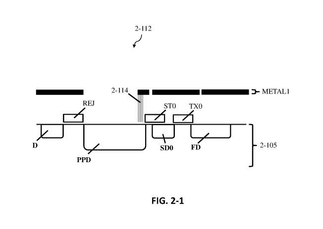
[0150] FIG. 2-1 is a schematic of pixel 2-112 including an optical barrier,
the optical barrier
including contact 2-114, according to some embodiments. In some embodiments,
pixel 2-112
may be configured in the manner described for pixel 1-112 in connection with
FIGs. 1-1A to 1-
1D, such as including substrate 2-105, photodetection region PPD, drain D,
storage bin SDO,
readout region FD, transfer gates REJ, STO, and TX0, and metal layer METALL As
shown in
FIG. 2-1, contact 2-114 is elongated from metal layer METAL1 to photodetection
region PPD.
Contact 2-114 may include an opaque material such as metal. In some
embodiments, the contact
may be formed using tungsten. Accordingly, contact 2-114 may be configured to
block at least
some secondary path photons incident on storage bin SDO. 2-32-4A2-4BIn some
embodiments,
contact 2-114 may have openings, such as to accommodate electrical routing in
and/or around
contact 2-114. As shown in FIG. 2-1, contact 2-114 extends toward but does not
physically
contact photodetection region PPD. In some embodiments, contact 2-114 may not
electrically
couple to the semiconductor region of the photodetection region PPD. For
example, primary
optical path coupling (e.g., from the sample well to photodetection region
PPD) and primary
electrical path coupling (e.g., from photodetection region PPD to storage bin
SDO) may be
isolated from one another. In some embodiments, a dielectric layer (e.g. film)
may be disposed
between contact 1-114 and photodetection PPD to isolate electrical voltage at
contact 2-114 from
18
CA 03144668 2021-12-21
WO 2020/264331 PCT/US2020/039868
photodetection region PPD. In some embodiments, the dielectric layer may be an
oxide gap
(e.g., having a width of 20 nm or wider in a 0.18um process node) positioned
between the bottom
of the contact and photodetection region PPD.
[0151] In some embodiments (e.g., FIGs. 2-3, 2-4A, and 2-1F), multiple
contacts 2-114 may be
positioned adjacent one another. In some embodiments, the contact may include
a continuous
strip of at least partially opaque material. In some embodiments, the contact
may form a wall
(e.g., FIGs. 2-4B to 2-1G). Although not shown in FIG. 2-1, pixel 2-112 may
include a plurality
of metal layers.
[0152] FIG. 2-2A is a schematic of pixel 2-212 including contacts 2-214a-b as
an optical barrier,
according to some embodiments. FIG. 2-2B is a top view of a portion of
integrated device 2-202
having a plurality of pixels including pixel 2-212, according to some
embodiments. FIG. 2-2A is
taken along cross-section A-A' of pixel 2-212, as shown in FIG. 2-2B. In some
embodiments,
pixel 2-212 may be configured in the manner described for pixel 1-112 in
connection with FIGs.
1-1A to 1-1D, such as including substrate 2-205, photodetection region PPD,
storage bin SDO,
readout region FD, transfer gates REJ, STO, and TX0, and metal layer METALL
Also shown in
FIGs. 2-2A and 2-2B are contacts 2-214a and 2-214b, which may be separate
contacts. For
example, as shown in FIG. 2-2B, contacts 2-214a and 2-214b may be elongated
across multiple
pixels in a row or column of pixels. As described for contact 2-114 in
connection with FIG. 2-1,
contacts 2-214a and 2-214b may be elongated from metal layer METAL1 to
substrate 2-205
without physically contacting substrate 2-205 or photodetection region PPD.
For example, a
dielectric layer (not shown) may be positioned between contacts 2-214a and 2-
214b and substrate
2-205 or photodetection region PPD. Contacts 2-214a and 2-214b may be
electrically isolated
from substrate 2-205 or photodetection region PPD. In some embodiments,
contacts 2-214a and
2-214b may be formed using an at least partially opaque material such as a
metal (e.g., tungsten).
[0153] FIGs. 2-2A and 2-2B also show contacts 2-216a-c, which may be
configured to
electrically couple to transfer gates STO and TX0 and readout region FD,
respectively. As shown
in FIG. 2-2B, each contact 2-216a-c may be positioned only in pixel 2-212
(e.g., with other
corresponding contacts in the other illustrated pixels). Also shown in FIGs. 2-
2A and 2-2B,
contacts 2-216a-c may physically contact transfer gates STO and TX0 and
readout region FD,
respectively. For example, contacts 2-216a-b may be configured to provide
control signals (e.g.,
from a control circuit) for biasing transfer gates STO and TX0 to cause charge
carriers to flow
from photodetection region PPD to storage bin SDO or from storage bin SDO to
readout region
FD, respectively. In this example, contact 2-216c may be configured to provide
charge carriers
from readout region FD to other portions of the integrated device for
processing. Techniques for
19
CA 03144668 2021-12-21
WO 2020/264331 PCT/US2020/039868
manufacturing contacts 2-214a-b and contacts 2-216a-c are described further
herein including
with reference to FIGs. 6-1A to 6-1B and 6-2A to 6-2B. Although not shown in
FIG. 2-2, pixel
2-212 may include a plurality of metal layers.
[0154] FIG. 2-3 is a schematic of pixel 2-312 including contact 2-314 as an
optical barrier,
where contact 2-314 is coupled to transfer gate STO, according to some
embodiments. In some
embodiments, pixel 2-312 may be configured in the manner described for pixel 1-
112 in
connection with FIGs. 1-1A to 1-1D, such as including substrate 2-305,
photodetection region
PPD, drain D, storage bin SDO, readout region FD, transfer gates REJ, STO, and
TX0, and metal
layer METAL 1. In contrast to pixel 2-112, contact 2-314 is at least partially
disposed around
transfer gate STO. In some embodiments, contact 2-314 may be electrically
coupled to transfer
gate STO. In some embodiments, contact 2-314 may be electrically isolated from
photodetection
region PPD and/or the bulk semiconductor region of substrate 2-305. Similar to
pixel 2-112, the
contact of pixel 2-312 may include an opaque material and/or metal, such as
tungsten.
Accordingly, contact 2-314 of pixel 2-312 may provide optical rejection of
secondary path
photons incident on storage bin SDO. In some embodiments, multiple contacts 2-
314 may be
disposed on opposite sides of photodetection region PPD, such as with one
contact 2-314
coupled to transfer gate STO and one contact 2-314 coupled to transfer gate
REJ.
[0155] FIG. 2-4A is a schematic of pixel 2-412a including contact wall 2-414
and via walls 2-
416a-c as an optical barrier, according to some embodiments. In FIG 2-4A,
contact wall 2-414 is
disposed between transfer gates REJ and STO and metal layer METAL1. As shown
in FIG. 2-
4A, first portion 2-414a of contact wall 2-414 is elongated from transfer gate
REJ to first metal
layer METAL1, and second portion 2-414b of contact wall 2-414 is elongated
from transfer gate
STO to metal layer METAL1. In addition, pixel 2-412 includes via walls 2-416a,
2-416b, and 2-
416c provided between adjacent metal layers, with via wall 2-416a elongated
from fourth metal
layer METAL4 to third metal layer METAL3, via wall 2-416b elongated from third
metal layer
METAL3 to second metal layer METAL2, and via wall 2-416c elongated from second
metal
layer METAL2 to first metal layer METAL 1.
[0156] FIG. 2-4B is a perspective view of pixel 2-412b including contact wall
2-414 as an
optical barrier, according to some embodiments. In some embodiments, pixel 2-
412b may be
configured in the manner described for pixel 2-412a in connection with FIG. 2-
4A, such as
including substrate 2-405, photodetection region PPD, storage bin SDO,
transfer gate STO, and
metal layers METAL1 and METAL2. Pixel 2-412b further includes contacts 2-418
elongated
between metal layer METAL1 and transfer gate STO. In some embodiments,
contacts 2-418 may
be configured to electrically couple metal layer METAL1 and transfer gate STO.
As shown in
CA 03144668 2021-12-21
WO 2020/264331 PCT/US2020/039868
FIG. 2-4B, contact wall 2-414 forms a cylindrical wall about photodetection
region PPD.
Accordingly, contact wall 2-414 may block secondary path photons incident on
storage bin SDO
and secondary path photons incident on storage bins that may be disposed on
other sides of
photodetection region PPD. It should be appreciated that contact wall 2-414
may form a
rectangular or octagonal wall rather than a cylindrical wall. Further,
multiple contact walls 2-414
may be disposed around photodetection region PPD. In some embodiments, pixel 2-
412b may
include one or more via walls elongated between metal layers 1 and 2 and/or
other metal layers.
[0157] FIG. 2-4C is a perspective view of pixel 2-412c including contact wall
2-414, via walls 2-
416a-d, and contacts 418, according to some embodiments. In some embodiments,
pixel 2-412b
may be configured in the manner described for pixel 2-412a in connection with
FIG. 2-4A, such
as including storage bin STO, substrate 2-405, and metal layers METAL1-4. In
FIG. 2-4C, pixel
2-412 includes contact wall 2-414 elongated from a dielectric layer 2-422,
disposed on the bulk
semiconductor region of substrate 2-405, to metal layer METALl. Pixel 2-412
further includes
via wall 2-416a-d elongated between metal layers METAL1-4 as described for
pixel 2-412b in
connection with FIG. 2-4B. As shown in FIG. 2-4C, contact wall 2-414 and via
walls 2-416a-d
may wrap cylindrically about photodetection region PPD. Also shown in FIG. 2-
4C are contacts
2-418 positioned between transfer gate STO and metal layer METALL In some
embodiments,
contacts 2-418 may be configured to electrically couple transfer gate STO to
metal layer
METALl. It should be appreciated that contact wall 2-414 and/or via walls 2-
416a-d may form
rectangular or octagonal walls rather than cylindrical walls.
[0158] It should be appreciated that contacts described herein may be
positioned above/below,
adjacent to, and/or within transfer gates of the pixel. For example, in some
embodiments, metal
may be positioned within the transfer gates to block at least some secondary
optical path photons
from reaching the storage bins.
[0159] FIG. 2-5 is a schematic of pixel 2-512 including metal layer METALO as
an optical
barrier, according to some embodiments. In some embodiments, pixel 2-512 may
be configured
in the manner described for pixel 2-112 in connection with FIGs. 1-1A to 1-1D,
such as
including substrate 2-505, photodetection region PPD, drain D, storage bin
SDO, readout region
FD, transfer gates REJ, STO, and TX0, and metal layer METALl. As shown in FIG.
2-5, metal
layer METALO is disposed around transfer gates STO and TX0. It should be
appreciated that, in
some embodiments, METALO may be disposed only around transfer gate STO, or
alternatively,
only around transfer gate TX0.
[0160] Metal layer METALO may include any suitable metal such as tungsten.
Accordingly,
metal layer METALO may block at least some secondary path photons from
reaching storage bin
21
CA 03144668 2021-12-21
WO 2020/264331 PCT/US2020/039868
SDO. In some embodiments, metal layer METALO may be only partially disposed
around
transfer gate STO and/or transfer gate TX0. In some embodiments, metal layer
METALO may be
alternatively or additionally disposed around transfer gate REJ (e.g., shown
in FIGs. 6-2A and 6-
2B). In some embodiments, METALO may be mechanically and/or electrically
coupled to a
contact and/or via, such as to provide combined optical isolation. For
example, the contact
and/or via may be elongated from metal layer METAL1 to metal layer METAL 0.
Although not
shown in FIG. 2-5, pixel 2-512 may include a plurality of metal layers.
[0161] FIG. 2-6 is a schematic of pixel 2-612 including metal transfer gates
STO and TX0 as an
optical barrier, according to some embodiments. In some embodiments, pixel 2-
612 may be
configured in the manner described for pixel 2-112 in connection with FIGs. 1-
1A to 1-1D, such
as including substrate 2-605, photodetection region PPD, drain D, storage bin
SDO, readout
region FD, transfer gates REJ, STO, and TX0, and metal layer METALL In
contrast to FIGs. 2-1
to 2-2, which may use predominantly polysilicon transfer gates, transfer gates
STO and TX0 are
composed of metal. For example, transfer gate STO and/or TX0 may include
between 75% to
99% metal, or 99% to 100% metal. Accordingly, transfer gates STO and TX0 may
be at least
partially opaque for blocking secondary path photons from reaching storage bin
SDO. It should
be appreciated that, in some embodiments, only one of transfer gates STO and
TX0 include
metal. In some embodiments, transfer gates STO and TX0 may contain different
amounts of
metal. Although not shown in FIG. 2-6, pixel 2-612 may include a plurality of
metal layers.
[0162] FIG. 2-7 is a schematic of pixel 2-712 including at least partially
opaque layers 2-714a
and 2-714b as an optical barrier, according to some embodiments. In some
embodiments, pixel
2-712 may be configured in the manner described for pixel 2-112 in connection
with FIGs. 1-1A
to 1-1D, such as including substrate 2-705, photodetection region PPD, drain
D, storage bin SDO,
readout region FD, transfer gates REJ, STO, and TX0, and metal layer METALL In
FIG. 2-7,
transfer gate STO may include a semiconductor material such as polysilicon,
and at least partially
opaque layers 2-714a and 2-714b may include a silicide layer such as cobalt
silicide, and/or
titanium nitride. At least partially opaque layer 2-714a may fully cover
transfer gate STO (e.g.,
on top and three sides), such as shown in FIG. 2-7, and/or may partially cover
transfer gate STO
(e.g., on a single surface). At least partially opaque layer 2-714b may
partially cover transfer
gate TX0, such as shown in FIG. 2-7, and/or may fully cover transfer gate TX0.
Accordingly, at
least partially opaque layers 2-714a and 2-714b may block at least some
secondary path photons
from reaching storage bin SDO. It should be appreciated that any number of
transfer gate
surfaces may be covered by one or multiple opaque layers. In some embodiments,
only transfer
22
CA 03144668 2021-12-21
WO 2020/264331 PCT/US2020/039868
gate STO or TX0 may be covered by an at least partially opaque layer. Although
not shown in
FIG. 2-7, pixel 2-712 may include a plurality of metal layers.
[0163] FIG. 2-8A is a plan view of pixel 2-812 having pillar array 2-816 as an
optical barrier.
FIG. 2-8B is a perspective view of pixel 2-812. In some embodiments, pixel 2-
812 may be
configured in the manner described for pixel 2-112 in connection with FIGs. 1-
1A to 1-1D, such
as including photodetection region PPD, substrate 2-805, and transfer gate
STO. In FIGs. 2-8A
and 2-8B, pillars of pillar array 2-816 are arranged in periodic patterns
within transfer gate STO.
Pillars 2-816 may include an optically transparent or opaque material. For
example, pillar array
2-816 may be configured to provide a contrast in refractive index compared to
a material of
transfer gate STO. In some embodiments, pillar array 2-816 may be arranged as
a two-
dimensional photonic crystal, which may block propagation of light inside
transfer gate STO and
reject photons incident along one or more secondary optical paths. Also shown
in FIGs. 2-8A
and 2-8B are contact wall 814a, which is disposed cylindrically about
photodetection region
PPD, and contacts 2-814b, which may be elongated between a metal layer (not
shown) and
transfer gate STO. In some embodiments, contacts 2-814b may be configured to
electrically
couple the metal layer to transfer gate STO. In some embodiments, a bulk
semiconductor region
of substrate 2-805 below transfer gate STO may include an array of pillars
arranged in a pattern
configured to block photons due to light that may diffract at an edge of
transfer gate STO. For
example, photons of the diffracted light may propagate towards storage bin SDO
along a
secondary optical path. In some embodiments, an interface at the edge of
transfer gate STO may
include a passivation structure, such as to limit dark current. It should be
appreciated that any
number of pillars may be used.
[0164] FIG. 2-9A is a plan view of pixel 2-912 having line array 2-916 as an
optical barrier,
according to some embodiments. FIG. 2-9B is a perspective view of pixel 2-912,
according to
some embodiments. In some embodiments, pixel 2-912 may be configured in the
manner
described for pixel 2-812 in connection with FIGs. 2-8A and 2-8B, such as
including
photodetection region PPD, substrate 2-905, and transfer gate STO. In FIGs. 2-
9A and 2-9B,
lines of line array 2-916 are arranged in periodic patterns within transfer
gate STO. Line array 2-
916 may include a transparent or opaque material and create a contrast in
refractive index with
material of transfer gate STO. In some embodiments, line array 2-916 may be
arranged in a one-
dimensional photonic crystal, which may block propagation of light inside
transfer gate STO and
reject photons incident along one or more secondary optical paths. Thus, line
array 2-916 may
be configured to block at least some secondary path photons from reaching
storage bins SDO
and/or SD1, as described herein for pillars array 2-816. Also shown in FIGs. 2-
9A and 2-9B are
23
CA 03144668 2021-12-21
WO 2020/264331 PCT/US2020/039868
contact wall 2-914a, which is disposed cylindrically about photodetection
region PPD, and
contacts 2-914b, which may be elongated between a metal layer (not shown) and
transfer gate
STO. In some embodiments, an array of lines may be included in a bulk
semiconductor region of
substrate 2-905 below transfer gate STO, as described for the pillars in
connection with FIG. 2-
8A. It should be appreciated that any number of lines may be used.
[0165] FIG. 2-10A is a plan view of pixel 2-1012 having optical waveguide 2-
1014 as an optical
barrier, according to some embodiments. FIG. 2-10B is a perspective view of
pixel 2-1012
according to some embodiments. In some embodiments, pixel 2-1012 may be
configured in the
manner described for pixel 2-112 in connection with FIGs. 1-1A to 1-1D, such
as including
substrate 2-1005, transfer gate STO, and metal layers METAL1-4. In FIGs. 2-10A
and 2-10B,
optical waveguide 1014 is positioned above photodetection region PPD (not
shown). For
example, optical waveguide 1014 may be positioned in an aperture (e.g.,
surrounded by metal
layers METAL1-4). Optical waveguide 1014 may have a higher (or lower)
refractive index
compared to the surrounding dielectric. Consequently, optical waveguide 1014
may direct light
to photodetection region PPD and reduce the number of secondary optical path
photons
propagating towards storage bins SDO and/or SD1 (not shown). Thus, optical
waveguide 1014
may block at least some secondary optical path photons from reaching storage
bins of pixel 2-
1012. In some embodiments, optical waveguide 1014 may have a cylindrical
geometry
extending from a surface of photodetection region PPD to a metal layer (e.g.,
METAL4). In
some embodiments, optical waveguide 1014 may have an oval cross section and/or
have a height
different from that of pixel 2-1012. It should be appreciated that any form of
optical waveguide
may be used, such as having a rectangular cross section, for example.
[0166] FIG. 2-10C is a graph 2-1000 of isolation ratio between a storage bin
of pixel 2-1012
(e.g., SDO and/or SD1) to photodetection region PPD versus refractive index of
optical
waveguide 1014, according to some embodiments. As shown in FIG. 2-10C, when
the refractive
index of optical waveguide 1014 is between 1.75 and 1.9 or 1.95, an isolation
ratio higher than
10,000 may be achieved.
[0167] IV. Techniques for Electrical Rejection
[0168] As described herein, the inventors have developed techniques for
rejecting secondary
electrical path charge carriers from reaching the storage bin(s) and impacting
signal quality.
Techniques described herein include implementing one or more semiconductor
wells or barriers
in a pixel and/or resizing and/or reshaping the storage bin(s) to reduce
attraction and increase
attenuation of secondary electrical path charge carriers to the storage
bin(s). Any or each pixel
described herein may be included in an integrated device (e.g., integrated
device 102). It should
24
CA 03144668 2021-12-21
WO 2020/264331 PCT/US2020/039868
be appreciated that techniques for secondary electrical path rejection may
also be useful for
secondary optical path rejection.
[0169] FIG. 3-1 is a schematic view of pixel 3-112 including doped
semiconductor well W as an
electrical barrier, according to some embodiments. In some embodiments, pixel
3-112 may be
configured in the manner described for pixel 1-112 in connection with FIGs. 1-
1A to 1-1D, such
as including substrate 3-105, photodetection region PPD, drain D, storage bin
SDO, readout
region FD, and transfer gates REJ, STO, and TX0. In FIG. 3-1, doped
semiconductor well W is
positioned below storage bin SDO. In some embodiments, doped semiconductor
well W may
have a same conductivity type as photodetection region PPD and storage bin
SDO. For example,
photodetection region PPD, storage bin SDO, and doped semiconductor well W may
be n-doped.
In this example, substrate 3-105 may be lightly p-doped. Undesired charge
carriers positioned
below storage bin SDO may be more attracted to an electric field provided by
the doping
concentration of doped semiconductor well W than to storage bin SDO, resulting
in fewer
undesired charge carriers entering storage bin SDO along secondary electrical
paths. It should be
appreciated that doped semiconductor well W is considered to be below storage
bin SDO when
doped semiconductor well W is positioned on an opposite side of storage bin
SDO from transfer
gate STO. Further, in embodiments with multiple storage bins, a doped
semiconductor well may
be positioned below each storage bin, or below some of the storage bins. In
some embodiments,
a single doped semiconductor well may be positioned below multiple storage
bins. In some
embodiments, substrate 3-105 may be lightly n-doped and photodetection region
PPD, storage
bin SDO, and doped semiconductor well W may be p-doped. Although not shown in
FIG. 3-1,
pixel 3-112 may include one or more metal layers.
[0170] FIG. 3-2 is a schematic view of pixel 3-212 including doped
semiconductor barrier B as
an electrical barrier, according to some embodiments. In some embodiments,
pixel 3-212 may
be configured in the manner described for pixel 1-112 in connection with FIGs.
1-1A to 1-1D,
such as including substrate 3-205, photodetection region PPD, drain D, storage
bin SDO, readout
region FD, and transfer gates REJ, STO, and TX0. In FIG. 3-2, doped
semiconductor barrier B is
positioned below storage bin SDO. In some embodiments, doped semiconductor
barrier may
have a different conductivity type from photodetection region PPD and storage
bin SDO. For
example, photodetection region PPD and storage bin SDO may be n-doped and
doped
semiconductor barrier B may be p-doped. In this example, substrate 3-205 may
be lightly p-
doped. In some embodiments, doped semiconductor barrier B may have a high
doping
concentration compared to bulk semiconductor regions of substrate 3-205
positioned around
storage bin SDO and/or doped semiconductor barrier B. Undesired photo-
electrons may be
CA 03144668 2021-12-21
WO 2020/264331 PCT/US2020/039868
blocked from reaching storage bin SDO when barrier B is positioned in the path
of the charge
carriers due to the electrical field provided by the doping concentration of
doped semiconductor
barrier B, resulting in fewer undesired charge carriers entering storage bin
SDO along secondary
electrical paths. It should be appreciated that, as described for
semiconductor well W, doped
semiconductor barrier B is considered to be below storage bin SDO when doped
semiconductor
barrier B is positioned on an opposite side of storage bin SDO from transfer
gate STO. Further, in
embodiments with multiple storage bins, a doped semiconductor barrier may be
positioned below
each storage bin, or below some of the storage bins. In some embodiments, a
single doped
semiconductor barrier may be positioned below multiple storage bins. In some
embodiments,
substrate 3-205 may be lightly n-doped, photodetection region PPD and storage
bin SDO may be
p-doped, and doped semiconductor barrier B may be n-doped. Although not shown
in FIG. 3-2,
pixel 3-212 may include one or more metal layers.
[0171] FIG. 3-3A is a plan view of pixel 3-312a including doped semiconductor
wells WO and
W1 as an electrical barrier, according to some embodiments. In some
embodiments, pixel 3-
312a may be configured in the manner described for pixel 1-112 in connection
with FIGs. 1-1A
to 1-1D, such as including photodetection region PPD and storage bins SDO and
SD1. In FIG. 3-
3A, doped semiconductor well WO is positioned adjacent storage bin SDO and
doped
semiconductor well W1 is positioned adjacent storage bin SD1. Doped
semiconductor wells WO
and W1 may be configured in the manner described for doped semiconductor well
W in
connection with FIG. 3-1, except that wells WO and W1 may be positioned
adjacent storage bins
SDO and SD1 rather than or in addition to being positioned below storage bins
SDO and/or SD1.
For example, doped semiconductor wells WO and W1 may be configured to attract
undesired
charge carriers along secondary paths from storage bin SDO to storage bin SD1.
Accordingly,
fewer undesired charge carriers may enter storage bins SDO and SD1 from the
adjacent sides. It
should be appreciated that doped semiconductor wells WO and/or W1 may be
included in pixels
having only a single storage bin.
[0172] FIG. 3-3B is a plan view of pixel 3-312b including doped semiconductor
wells W0i,
W02, W1 1, and W12 as an electrical barrier, according to some embodiments. In
some
embodiments, pixel 3-312b may be configured in the manner described for pixel
1-112 in
connection with FIGs. 1-1A to 1-1D, such as including photodetection region
PPD and storage
bins SDO and SD1. In FIG. 3-3B, doped semiconductor wells W01 and W02 are
positioned
adjacent storage bin SDO and doped semiconductor wells W1 1 and W12 are
positioned adjacent
storage bin SD1. Doped semiconductor wells W0i, W02, W1 1, and W12 may be
configured in
the manner described for doped semiconductor wells WO and W1 in connection
with FIG. 3-3A,
26
CA 03144668 2021-12-21
WO 2020/264331 PCT/US2020/039868
except that wells W0i, W02, W1 1, and W12 may be positioned on multiple sides
of each storage
bin SDO and SD1. For example, doped semiconductor wells W0i, W02, Wli, and W12
may
attract undesired charge carriers incident on storage bins SDO and Sdl from
multiple sides.
Accordingly, fewer undesired charge carriers may enter storage bins SDO and
SD1 from the
adjacent sides. It should be appreciated that doped semiconductor wells W0i,
W02, Wli, and/or
W12 may be included in pixels having only a single storage bin.
[0173] FIG. 3-4A is a plan view of pixel 3-412a including doped semiconductor
barriers BO and
B1 as an electrical barrier, according to some embodiments. In some
embodiments, pixel 3-412a
may be configured in the manner described for pixel 1-112 in connection with
FIGs. 1-1A to 1-
1D, such as including photodetection region PPD and storage bins SDO and SD1.
In FIG. 3-4A,
doped semiconductor barrier BO is positioned adjacent storage bin SDO and
doped semiconductor
barrier B1 is positioned adjacent storage bin Bl. Doped semiconductor barriers
BO and B1 may
be configured in the manner described for doped semiconductor barrier B in
connection with
FIG. 3-2, except that barriers BO and B1 may be positioned adjacent storage
bins SDO and SD1
rather than or in addition to being positioned below storage bins SDO and SD1.
For example,
doped semiconductor barriers BO and B1 may be configured to block undesired
charge carriers
along secondary paths from storage bin SDO to storage bin SD1. Accordingly,
fewer undesired
charge carriers may enter storage bins SDO and SD1 from the adjacent sides. It
should be
appreciated that doped semiconductor barriers BO and/or B1 may be included in
pixels having
only a single storage bin.
[0174] FIG. 3-4B is a plan view of pixel 3-412b including doped semiconductor
barriers B01,
B02, Bli, and B12 as an electrical barrier, according to some embodiments. In
some
embodiments, pixel 3-412b may be configured in the manner described for pixel
1-112 in
connection with FIGs. 1-1A to 1-1D, such as including photodetection region
PPD and storage
bins SDO and SD1. In FIG. 3-4B, doped semiconductor barriers B01 and B02 are
positioned
adjacent storage bin SDO and doped semiconductor barriers Bli and B12 are
positioned adjacent
storage bin SD1. Doped semiconductor barriers B01, B02, Bli, and Bl2may be
configured in the
manner described for doped semiconductor barriers BO and B1 in connection with
FIG. 3-4A,
except that doped semiconductor barriers B01, B02, Bli, and B12 may be
positioned on multiple
sides of each storage bin SDO and SD1. For example, doped semiconductor
barriers B01, B02,
Bli, and B12 may block undesired charge carriers incident on storage bins SDO
and Sdl from
multiple sides. Accordingly, fewer undesired charge carriers may enter storage
bins SDO and
SD1 from the adjacent sides. It should be appreciated that doped semiconductor
barriers B01,
B02, Bli, and B12 may be included in pixels having only a single storage bin.
27
CA 03144668 2021-12-21
WO 2020/264331 PCT/US2020/039868
[0175] It should be appreciated that optical and electrical rejection
techniques may be
implemented alone or in combination, such as shown in FIG. 3-5.
[0176] FIG. 3-5 is a schematic view of pixel 3-512 including doped
semiconductor barrier B as
an electrical barrier, according to some embodiments. In some embodiments,
pixel 3-512 may
be configured in the manner described for pixel 1-112 in connection with FIGs.
1-1A to 1-1D,
such as including substrate 3-505, photodetection region PPD, storage bin SDO,
readout region
FD, transfer gates STO and TX0, and metal layer METALL Also shown in FIG. 3-5,
are contact
walls 3-514a and 3-514b and contacts 3-516a-c, which may be configured in the
manner
described for contact walls 2-214a-b and contacts 2-216a-c, respectively, in
connection with
FIGs. 2-2A and 2-2B. In some embodiments, doped semiconductor barrier B may be
configured
in the manner described in connection with FIG. 3-2. Although only metal layer
METAL1 is
shown, it should be appreciated that pixel 3-512 may include a plurality of
metal layers.
[0177] The inventors have also developed techniques for configuring the
storage bins relative to
the photodetection region to impede secondary optical path photons and/or
secondary electrical
path (e.g., noise) charge carriers from reaching the storage bins. The storage
bins may be shaped
to perform such impeding and/or located relative to the photodetection region
to perform such
impeding. In some embodiments, storage bins may be positioned to increase the
potential barrier
charge carriers encounter en route to the storage bins. For example, the
inventors recognized that
by positioning the storage bins farther from the photodetection region, the
potential barrier may
be increased to a level acceptable for fluorescent emission charge carriers
but sufficient to
impede noise charge carriers. In some embodiments, the primary electrical path
for desired
charge carriers may be a straight line from the photodetection region to the
storage bins, whereas
secondary electrical paths for undesired charge carriers may be diagonal lines
from the bulk
semiconductor region adjacent and/or below the primary path. Accordingly, the
secondary
electrical paths may be longer than the primary electrical path such that
positioning the storage
bins farther from the photodetection region results in more attenuation of the
secondary electrical
paths than the primary electrical path. Thus, undesired charge carriers may be
attenuated without
losing desired charge carriers. Moreover, in some embodiments, the primary
optical path from
the sample to the photodetection region may be a straight line, whereas
secondary optical paths
to the storage bins may be diagonal paths that are longer than the primary
optical path.
Accordingly, positioning the storage bins farther from the photodetection
region may cause
fewer secondary optical path photons to reach the storage bins, for example,
due to path
obstruction and/or attenuation. Thus, some techniques described herein may
provide both optical
and electrical secondary path rejection, rather than just optical or
electrical rejection. In some
28
CA 03144668 2021-12-21
WO 2020/264331 PCT/US2020/039868
embodiments, a doping concentration of the storage bins may be configured to
impede noise
charge carriers from reaching the storage bins. For example, the inventors
recognized that the
doping concentration of the storage bins may be decreased to reduce the
attraction of noise
charge carriers towards the storage bins.
[0178] FIG. 4-1 is a graph 4-100 of electric potential versus positioning
within portions of two
pixels, where first curve 4-102 is the electric potential within a portion of
the first pixel and
second curve 4-104 is the electric potential within a portion of the second
pixel, according to
some embodiments. As shown in FIG. 4-1, first curve 4-102 shows the electric
potential of a
pixel having storage bin SD0a and photodetection region PPD. The doping
profiles of
photodetection region PPD and storage bin SD0a may be configured to cause
concave-up regions
of first curve 4-102. For example, photodetection region PPD and storage bin
SDO may have
relatively high doping concentrations and opposite conductivity types from
surrounding bulk
regions of the pixel substrate. In FIG. 4-1, potential barrier La is
positioned between
photodetection region PPD and storage bin SD0a, shown as a concave-down region
of first curve
4-102. In some embodiments, potential barrier La may be created by the
difference in doping
concentration between storage bin SD0a and the pixel region in which potential
barrier La is
disposed. Second curve 4-104 shows the electric potential of a pixel having
storage bin SDOb
and photodetection region PPD, The doping profiles of photodetection region
PPD and storage
bin SDOb may be configured to cause concave-up regions of second curve 4-104.
For example,
photodetection region PPD and storage bin SDOb may have relatively high doping
concentrations
and opposite conductivity types from surrounding bulk regions of the pixel
substrate. In FIG. 4-
1, potential barrier Lb is positioned between photodetection region PPD and
storage bin SD0b,
shown as a concave-down region of second curve 4-102. In some embodiments,
potential barrier
Lb may be created by the difference in doping concentration between storage
bin SDOb and the
pixel region in which potential barrier Lb is disposed.
[0179] In FIG. 4-1, photodetection region PPD is positioned at approximately
the same location
in both pixels, whereas storage bin SDOb is spaced farther from photodetection
region PPD than
is storage bin SD0a. The spacings between photodetection region PPD and
storage bins SD0a
and SDOb are shown in FIG. 4-2.
[0180] FIG. 4-2 is a graph 4-200 of relative isolation versus storage bin to
photodetection region
spacing for the pixels of FIG. 4-1, according to some embodiments. As shown in
FIGs. 4-1 and
4-2, storage bin SDOb is positioned farther from photodetection region PPD
than storage bin
SD0a. In FIG. 4-2, storage bin SD0a is spaced between 1.5 and 2 microns from
photodetection
PPD, and storage bin SDOb is spaced between 2.25 and 2.5 microns from
photodetection region
29
CA 03144668 2021-12-21
WO 2020/264331 PCT/US2020/039868
PPD. In some embodiments, the larger spacing from photodetection region PPD to
storage bin
SDOb than to storage bin SD0a creates potential barrier Lb, which may be
configured to attract
fewer secondary electrical path charge carriers from photodetection region PPD
to storage bin
SD0b. Moreover, because storage bin SD0b may be positioned farther from
photodetection
region PPD than is storage bin SD0a, secondary electrical path charge carriers
propagating inside
the bulk semiconductor region may travel farther to reach storage bin SD0b
than to reach storage
bin SD0a. As a result, loss (e.g., due to attenuation) for such charge
carriers in the bulk
semiconductor region may be higher, reducing the number of charge carriers
that reach storage
bin SD0b. Likewise, for secondary optical path photons that propagate in the
space between the
bulk semiconductor region and the first metal layer, the increased distance to
reach storage bin
SD0b results in higher absorption along the secondary optical path, such that
fewer secondary
optical path photons may reach storage bin SD0b. It should be appreciated that
distances shown
in FIG. 4-2 are exemplary and other distances may be implemented.
[0181] FIG. 4-3 is a schematic view of pixel 4-312 having storage bin SD0c
with reduced depth,
according to some embodiments. In some embodiments, pixel 3-212 may be
configured in the
manner described for pixel 1-112 in connection with FIGs. 1-1A to 1-1D, such
as including
substrate 4-305, photodetection region PPD, drain D, storage bin SD0c, readout
region FD, and
transfer gates REJ, STO, and TX0. In FIG. 4-3, doped semiconductor region S is
positioned
below storage bin SD0c. In some embodiments, doped semiconductor region S may
have an
opposite conductivity type from photodetection region PPD and storage bin
SD0c. For example,
photodetection region PPD and storage bin SD0c may be n-doped regions and
doped
semiconductor region S may be a p-doped region such that storage bin SD0c has
a shallower
depth with respect to transfer gate STO than without doped semiconductor
region S. In this
example, substrate 4-305 may be lightly p-doped. The potential difference
between storage bin
SD0c and doped semiconductor region S may create a barrier for secondary
electrical path
charge carriers and/or secondary optical path photons incident on storage bin
SD0c.
Accordingly, fewer undesired charge carriers may be generated in storage bin
SD0c, and/or
fewer secondary optical path photons may reach storage bin SD0c. In some
embodiments, an n-
doped semiconductor region may be positioned below semiconductor region S to
attract
undesired charge carriers away from storage bin SD0c, resulting in fewer
charge carriers
reaching storage bin SD0c along secondary electrical paths. It should be
appreciated that, in
some embodiments, photodetection region PPD and storage bin SD0c may be p-
doped, doped
semiconductor region S may be n-doped, and substrate 4-305 may be lightly n-
doped. Although
not shown in FIG. 4-3, pixel 4-312 may include one or more metal layers.
CA 03144668 2021-12-21
WO 2020/264331 PCT/US2020/039868
[0182] FIG. 4-4 is a graph 4-400 of electric potential versus depth in two
pixels, where first
curve 4-402 is the electric potential of a pixel without doped semiconductor
region S and second
curve 4-404 is the electric potential of pixel 4-312 including doped
semiconductor region S,
according to some embodiments. Storage bin SD0a of the first pixel and storage
bin SDOc of
pixel 4-312 are indicated by concave-up regions of first and second curves 4-
402 and 4-404. As
shown in FIG. 4-4, the depth of storage bin SDOc is less than the depth of
storage bin SD0a.
Thus, secondary electrical charge carriers incident on storage bin SDOc from
below (e.g.,
diagonally from the bottom of photodetection region PPD, etc.) may have to
traverse a longer
distance to reach storage bin SDOc than they would to reach storage bin SD0a.
In FIG. 4-4,
doped semiconductor region S is indicated by the deep-side shoulder of storage
bin SDOc having
a higher electric potential than the portion of storage bin SD0a located at
the same depth.
[0183] V. Methods of Manufacture
[0184] The inventors have also developed techniques for manufacturing
integrated devices, as
described further herein. It should be appreciated that, other than where
specified, typical
complementary metal oxide semiconductor (CMOS) processes may be used to
produce the
devices.
[0185] FIGs. 6-1A to 6-1E are diagrams of steps 6-150 to 6-160 of an exemplary
method for
constructing contacts 2-214a-b and 2-216a-c of pixel 2-212 of FIGs. 2-2A and 2-
2B, according to
some embodiments. In FIGs. 6-1A to 6-1E, contact 6-114, which may be contact 2-
214a or 2-
214b of pixel 2-212, and contact 6-116, which may be contact 2-216a, 2-216b,
or 2-216c of pixel
2-212, are each deposited on a bulk semiconductor region of substrate 6-105.
At step 6-152
shown in FIG. 6-1A, the bulk semiconductor region has thereupon multi-layer
dielectric film
stack 6-172, which may be a contact etch stop layer (CESL), and an inter-layer
dielectric (ILD)
layer 6-174. For example, the bulk semiconductor region of substrate 6-105 may
include lightly
doped Silicon and dielectric film stack 6-172 may include silicon oxide (5i02)
and/or Silicon
Oxy-Nitride (SiON). At step 6-154 shown in FIG. 6-1B, first portion 6-176a of
ILD layer 6-174
and dielectric film stack 6-172 may be removed (e.g., etched), leaving at
least some of dielectric
film stack 6-172 atop the bulk semiconductor region of substrate 6-105. At
step 6-156 shown in
FIG. 6-1C, photoresist (PR) layer 6-178 may be placed over the location where
first portion 6-
176a was removed during step 6-154, and second portion 6-176b of ILD layer 6-
174 and
dielectric film stack 6-172 may be further removed subsequently (e.g.,
etched). Removing
second portion 6-176b may include removing all of oxide layer 6-172a of
dielectric film stack 6-
172 such that the bulk semiconductor region of substrate 6-105 is exposed. At
step 6-158 shown
in FIG. 6-1D, PR layer 6-178 may be removed. At step 6-160 shown in FIG. 6-1E,
a conductive
31
CA 03144668 2021-12-21
WO 2020/264331 PCT/US2020/039868
metal may be deposited in each of the locations from which first portion 6-
176a and second
portion 6-176b were removed to form contacts 6-114 and 6-116, respectively.
For example, each
contact 6-114 and 6-116 may include metal such as tungsten, titanium, titanium
nitride,
aluminum, aluminum/copper, nickel, or a layered combination of them. Because
the first
location from which first portion 6-176a was removed includes at least some of
dielectric film
stack 6-172 between contact 6-114 and the bulk semiconductor region of
substrate 6-105, contact
6-114 may be electrically isolated from the bulk semiconductor region of
substrate 6-105. In
contrast, because the bulk semiconductor region of substrate 6-105 is exposed
at the second
location from which second portion 6-176b was removed, contact 6-116 may be
electrically
coupled to the bulk semiconductor region of substrate 6-105 below.
[0186] It should be appreciated that the etching and metal deposit steps
described in connection
with FIGs. 6-1A to 6-1E may be performed in any order. For example, etching
and depositing
contact 6-116 may be performed prior to etching and depositing contact 6-114,
etching space for
contact 6-116 may be performed prior to etching space for contact 6-114,
and/or depositing
contact 6-116 may be performed prior to depositing contact 6-114, according to
various
embodiments. In some embodiments, contacts 6-114 and 6-116 may be deposited in
different
steps. In some embodiments, contact 6-114 may be formed using an at least
partially opaque
material and/or electrically insulative material.
[0187] FIGs. 6-2A to 6-2E are diagrams of steps 6-252 to 2-260 of an
alternative exemplary
method for constructing contacts 2-214a-b and 2-216a-c of pixel 2-212 of FIGs.
2-2A and 2-2B,
according to some embodiments. At steps 6-252 and 6-254 shown in FIGs. 6-2A
and 6-2B,
respectively, the bulk semiconductor region of substrate 6-205 includes
dielectric stack 6-272
and ILD layer 6-274, which may be configured in the manner described for
substrate 6-105,
dielectric stack 6-172, and ILD layer 2-174 in connection with FIG. 6-1A. In
some
embodiments, steps 6-252 and 6-254 may be performed in the manner described
for steps 6-152
and 6-154 in connection with FIGs. 6-1A and 6-1B, respectively with first
portion 6-276a being
removed from dielectric stack 6-272 and ILD layer 6-274. However, at step 6-
256 shown in
FIG. 6-2C, contact 6-214 may be deposited in the location from which first
portion 6-276a was
removed in step 6-154b. In some embodiments, contact 6-214 may include metal.
Alternatively
or additionally, contact 6-214 may include an optically opaque material. For
example, contact 6-
214 may not be electrically conductive. In some embodiments, a top surface of
contact 6-214
may be polished. Also at step 6-256, an additional dielectric layer (e.g.,
sacrificial layer) 6-280
may be deposited on top of contact 6-214 (e.g., on the polished surface) to
accommodate the PR
layer 6-278, shown in FIG. 6-2D. At step 6-258 shown in FIG. 6-2D, PR layer 6-
278 may be
32
CA 03144668 2021-12-21
WO 2020/264331 PCT/US2020/039868
placed and patterned for removing (e.g., etching) second portion 6-276b of ILD
layer 6-274 and
dielectric film stack 6-272. The bulk semiconductor region of substrate 6-205
may be exposed
upon removing second portion 6-287b of ILD layer 6-274 and dielectric film
stack 6-272 to
enable electrical coupling with the bulk semiconductor region of substrate 6-
205. At step 6-160
shown in FIG. 6-2E, PR layer 6-278 may be removed and contact 6-216 may be
deposited in the
location from which second portion 6-176b was removed. Accordingly, contact 6-
216 may be
electrically coupled to the bulk semiconductor region of substrate 6-205.
[0188] It should be appreciated that the etching and metal deposit steps
described in connection
with FIGs. 6-2A to 6-2E may be performed in any order. For example, etching
and depositing
contact 6-216 may be performed prior to etching and depositing contact 6-214,
etching space for
contact 6-216 may be performed prior to etching space for contact 6-214,
and/or depositing
contact 6-216 may be performed prior to depositing contact 6-214, according to
various
embodiments.
[0189] FIGs. 6-3A to 6-3D are diagrams of an exemplary method for constructing
metal layer
METALO of pixel 2-512 of FIG. 2-5, according to some embodiments. At step 6-
352 shown in
FIG. 6-3A, transfer gates TX, STO, and REJ have dielectric film stack 6-372
and ILD layer 6-374
thereupon, which may be configured in the manner described for dielectric film
stack 6-172 and
ILD layer 6-174 in connection with FIG. 6-1A. For example, the dielectric film
stack may
include silicon oxide and SiON. At step 6-354 shown in FIG. 6-3B, first
portion of ILD 6-374
may be removed (e.g., etched). For example, first portion 6-376a may be
positioned above
transfer gates TX and STO. At step 6-356 shown in FIG. 6-3C, metal layer
METALO may be
deposited in the location from which first portion 6-376a of ILD layer 6-374
was removed. At
step 6-358 shown in FIG. 6-3D, second portion 6-376b of ILD layer 6-374 may be
removed and
contact 6-316 may be deposited over transfer gate REJ. In some embodiments,
contact 6-316
may be configured in the manner described for contact 6-116 in connection with
FIGs. 6-1A to
6-1E. Second portion 6-376b may include at least some of the SiON above
transfer gate REJ.
[0190] It should be appreciated that the etching and metal deposit steps
described in connection
with FIGs. 6-3A to 6-3D may be performed in any order. For example, etching
and depositing
metal layer METALO may be performed prior to etching and depositing contact 6-
316, etching
space for contact 6-316 may be performed prior to etching space for metal
layer METALO,
and/or depositing contact 6-316 may be performed prior to depositing metal
layer METALO,
according to various embodiments.
[0191] FIGs. 6-4A to 6-4C are diagrams of an alternative exemplary method for
constructing
metal layer METALO of pixel 2-512 of FIG. 2-5, according to some embodiments.
At step 6-452
33
CA 03144668 2021-12-21
WO 2020/264331 PCT/US2020/039868
shown in FIG. 6-3A, transfer gates TX, STO, and REJ have dielectric film stack
6-472 thereupon.
For example, dielectric film stack 6-472 may include insulative film including
SiON. At step 6-
454 shown in FIG. 6-4B, metal layer METALO may be deposited over at least one
of control
terminals TX, STO, and REJ and/or photodetection region PPD. At step 6-456
shown in FIG. 6-
4C, at least some of metal layer METALO may be removed (e.g., etched), such as
above control
terminals TX, STO, and/or REJ, and/or above photodetection region PD, readout
region FD,
and/or drain region D. In some embodiments, some of metal layer METALO may be
left above
readout region FD and/or photodetection region PD, such as shown in FIG. 6-4C.
At step 6-458,
contact 6-416 may be deposited. In some embodiments, contact 6-416 may be
configured in the
manner described for contact 6-116 in connection with FIGs. 6-1A to 6-1E. In
some
embodiments, ILD layer 6-474 may be deposited over the portions of metal layer
METALO that
were not removed at step 6-456, and contact 6-416 may be deposited above
control terminals
TX, STO, and/or REJ, with ILD layer 6-474 deposited above metal layer METALO.
In some
embodiments, ILD layer 6-474 may not be deposited above portions of metal
layer METALO
positioned above control terminal REJ.
[0192] It should be appreciated that the etching and metal deposit steps
described in connection
with FIGs. 6-4A to 6-4D may be performed in any order. For example, etching
and depositing
metal layer METALO may be performed prior to etching and depositing contact 6-
416, etching
space for contact 6-416 may be performed prior to etching space for metal
layer METALO,
and/or depositing contact 6-416 may be performed prior to depositing metal
layer METALO,
according to various embodiments.
[0193] VI. DNA and/or RNA Sequencing Applications
[0194] An analytic system described herein may include an integrated device
and an instrument
configured to interface with the integrated device. The integrated device may
include an array of
pixels, where a pixel includes a reaction chamber and at least one
photodetector. A surface of
the integrated device may have a plurality of reaction chambers, where a
reaction chamber is
configured to receive a sample from a suspension placed on the surface of the
integrated device.
A suspension may contain multiple samples of a same type, and in some
embodiments, different
types of samples. In this regard, the phrase "sample of interest" as used
herein can refer to a
plurality of samples of a same type that are dispersed in a suspension, for
example. Similarly,
the phrase "molecule of interest" as used herein can refer to a plurality of
molecules of a same
type that are dispersed in a suspension. The plurality of reaction chambers
may have a suitable
size and shape such that at least a portion of the reaction chambers receive
one sample from a
suspension. In some embodiments, the number of samples within a reaction
chamber may be
34
CA 03144668 2021-12-21
WO 2020/264331 PCT/US2020/039868
distributed among the reaction chambers such that some reaction chambers
contain one sample
with others contain zero, two or more samples.
[0195] In some embodiments, a suspension may contain multiple single-stranded
DNA
templates, and individual reaction chambers on a surface of an integrated
device may be sized
and shaped to receive a sequencing template. Sequencing templates may be
distributed among
the reaction chambers of the integrated device such that at least a portion of
the reaction
chambers of the integrated device contain a sequencing template. The
suspension may also
contain labeled nucleotides which then enter in the reaction chamber and may
allow for
identification of a nucleotide as it is incorporated into a strand of DNA
complementary to the
single-stranded DNA template in the reaction chamber. In some embodiments, the
suspension
may contain sequencing templates and labeled nucleotides may be subsequently
introduced to a
reaction chamber as nucleotides are incorporated into a complementary strand
within the reaction
chamber. In this manner, timing of incorporation of nucleotides may be
controlled by when
labeled nucleotides are introduced to the reaction chambers of an integrated
device.
[0196] Excitation light is provided from an excitation source located separate
from the pixel
array of the integrated device. The excitation light is directed at least in
part by elements of the
integrated device towards one or more pixels to illuminate an illumination
region within the
reaction chamber. A marker may then emit emission light when located within
the illumination
region and in response to being illuminated by excitation light. In some
embodiments, one or
more excitation sources are part of the instrument of the system where
components of the
instrument and the integrated device are configured to direct the excitation
light towards one or
more pixels.
[0197] Emission light emitted from a reaction chamber (e.g., by a fluorescent
label) may then be
detected by one or more photodetectors within a pixel of the integrated
device. Characteristics of
the detected emission light may provide an indication for identifying the
marker associated with
the emission light. Such characteristics may include any suitable type of
characteristic, including
an arrival time of photons detected by a photodetector, an amount of photons
accumulated over
time by a photodetector, and/or a distribution of photons across two or more
photodetectors. In
some embodiments, a photodetector may have a configuration that allows for the
detection of
one or more timing characteristics associated with emission light (e.g.,
fluorescence lifetime).
The photodetector may detect a distribution of photon arrival times after a
pulse of excitation
light propagates through the integrated device, and the distribution of
arrival times may provide
an indication of a timing characteristic of the emission light (e.g., a proxy
for fluorescence
lifetime). In some embodiments, the one or more photodetectors provide an
indication of the
CA 03144668 2021-12-21
WO 2020/264331 PCT/US2020/039868
probability of emission light emitted by the marker (e.g., fluorescence
intensity). In some
embodiments, a plurality of photodetectors may be sized and arranged to
capture a spatial
distribution of the emission light. Output signals from the one or more
photodetectors may then
be used to distinguish a marker from among a plurality of markers, where the
plurality of
markers may be used to identify a sample or its structure. In some
embodiments, a sample may
be excited by multiple excitation energies, and emission light and/or timing
characteristics of the
emission light from the reaction chamber in response to the multiple
excitation energies may
distinguish a marker from a plurality of markers.
[0198] A schematic overview of the system 5-100 is illustrated in FIG. 5-1A.
The system
comprises both an integrated device 5-102 that interfaces with an instrument 5-
104. In some
embodiments, instrument 5-104 may include one or more excitation sources 5-106
integrated as
part of instrument 5-104. In some embodiments, an excitation source may be
external to both
instrument 5-104 and integrated device 5-102, and instrument 5-104 may be
configured to
receive excitation light from the excitation source and direct excitation
light to the integrated
device. The integrated device may interface with the instrument using any
suitable socket for
receiving the integrated device and holding it in precise optical alignment
with the excitation
source. The excitation source 5-106 may be configured to provide excitation
light to the
integrated device 5-102. As illustrated schematically in FIG. 5-1A, the
integrated device 5-102
has a plurality of pixels 5-112, where at least a portion of pixels may
perform independent
analysis of a sample of interest. Such pixels 5-112 may be referred to as
"passive source pixels"
since a pixel receives excitation light from a source 5-106 separate from the
pixel, where
excitation light from the source excites some or all of the pixels 5-112.
Excitation source 5-106
may be any suitable light source. Examples of suitable excitation sources are
described in U.S.
Pat. Application No. 14/821,688, filed August 7, 2015, titled "INTEGRATED
DEVICE FOR
PROBING, DETECTING AND ANALYZING MOLECULES," which is incorporated by
reference in its entirety. In some embodiments, excitation source 5-106
includes multiple
excitation sources that are combined to deliver excitation light to integrated
device 5-102. The
multiple excitation sources may be configured to produce multiple excitation
energies or
wavelengths.
[0199] A pixel 5-112 has a reaction chamber 5-108 configured to receive a
single sample of
interest and a photodetector 5-110 for detecting emission light emitted from
the reaction chamber
in response to illuminating the sample and at least a portion of the reaction
chamber 5-108 with
excitation light provided by the excitation source 5-106. In some embodiments,
reaction
chamber 5-108 may retain the sample in proximity to a surface of integrated
device 5-102, which
36
CA 03144668 2021-12-21
WO 2020/264331 PCT/US2020/039868
may ease delivery of excitation light to the sample and detection of emission
light from the
sample or a reaction component (e.g., a labeled nucleotide).
[0200] Optical elements for coupling excitation light from excitation light
source 5-106 to
integrated device 5-102 and guiding excitation light to the reaction chamber 5-
108 are located
both on integrated device 5-102 and the instrument 5-104. Source-to-chamber
optical elements
may comprise one or more grating couplers located on integrated device5-102 to
couple
excitation light to the integrated device and waveguides to deliver excitation
light from
instrument 5-104 to reaction chambers in pixels 5-112. One or more optical
splitter elements
may be positioned between a grating coupler and the waveguides. The optical
splitter may
couple excitation light from the grating coupler and deliver excitation light
to at least one of the
waveguides. In some embodiments, the optical splitter may have a configuration
that allows for
delivery of excitation light to be substantially uniform across all the
waveguides such that each
of the waveguides receives a substantially similar amount of excitation light.
Such embodiments
may improve performance of the integrated device by improving the uniformity
of excitation
light received by reaction chambers of the integrated device.
[0201] Reaction chamber 5-108, a portion of the excitation source-to-chamber
optics, and the
reaction chamber-to-photodetector optics are located on integrated device 5-
102. Excitation
source 5-106 and a portion of the source-to-chamber components are located in
instrument 5-
104. In some embodiments, a single component may play a role in both coupling
excitation light
to reaction chamber 5-108 and delivering emission light from reaction chamber
5-108 to
photodetector 5-110. Examples of suitable components, for coupling excitation
light to a
reaction chamber and/or directing emission light to a photodetector, to
include in an integrated
device are described in U.S. Pat. Application No. 14/821,688, filed August 7,
2015, titled
"INTEGRATED DEVICE FOR PROBING, DETECTING AND ANALYZING
MOLECULES," and U.S. Pat. Application No. 14/543,865, filed November 17, 2014,
titled
"INTEGRATED DEVICE WITH EXTERNAL LIGHT SOURCE FOR PROBING,
DETECTING, AND ANALYZING MOLECULES," both of which are incorporated by
reference in their entirety.
[0202] Pixel 5-112 is associated with its own individual reaction chamber 5-
108 and at least one
photodetector 5-110. The plurality of pixels of integrated device 5-102 may be
arranged to have
any suitable shape, size, and/or dimensions. Integrated device 5-102 may have
any suitable
number of pixels. The number of pixels in integrated device 2-102 may be in
the range of
approximately 10,000 pixels to 1,000,000 pixels or any value or range of
values within that
range. In some embodiments, the pixels may be arranged in an array of 512
pixels by 512 pixels.
37
CA 03144668 2021-12-21
WO 2020/264331 PCT/US2020/039868
Integrated device 5-102 may interface with instrument 5-104 in any suitable
manner. In some
embodiments, instrument 5-104 may have an interface that detachably couples to
integrated
device 5-102 such that a user may attach integrated device 5-102 to instrument
5-104 for use of
integrated device 5-102 to analyze at least one sample of interest in a
suspension and remove
integrated device 5-102 from instrument 5-104 to allow for another integrated
device to be
attached. The interface of instrument 5-104 may position integrated device 5-
102 to couple with
circuitry of instrument 5-104 to allow for readout signals from one or more
photodetectors to be
transmitted to instrument 5-104. Integrated device 5-102 and instrument 5-104
may include
multi-channel, high-speed communication links for handling data associated
with large pixel
arrays (e.g., more than 10,000 pixels).
[0203] A cross-sectional schematic of integrated device 5-102 illustrating a
row of pixels 5-112
is shown in FIG. 5-1B. Integrated device 5-102 may include coupling region 5-
201, routing
region 5-202, and pixel region 5-203. Pixel region 5-203 may include a
plurality of pixels 5-112
having reaction chambers 5-108 positioned on a surface at a location separate
from coupling
region 5-201, which is where excitation light (shown as the dashed arrow)
couples to integrated
device 5-102. Reaction chambers 5-108 may be formed through metal layer(s) 5-
116. One pixel
5-112, illustrated by the dotted rectangle, is a region of integrated device 5-
102 that includes a
reaction chamber 5-108 and a photodetection region having one or more
photodetectors 5-110.
[0204] FIG. 5-1B illustrates the path of excitation (shown in dashed lines) by
coupling a beam of
excitation light to coupling region 5-201 and to reaction chambers 5-108. The
row of reaction
chambers 5-108 shown in FIG. 5-1B may be positioned to optically couple with
waveguide 5-
220. Excitation light may illuminate a sample located within a reaction
chamber. The sample or
a reaction component (e.g., fluorescent label) may reach an excited state in
response to being
illuminated by the excitation light. When in an excited state, the sample or
reaction component
may emit emission light, which may be detected by one or more photodetectors
associated with
the reaction chamber. FIG. 5-1B schematically illustrates the path of emission
light (shown as
the solid line) from a reaction chamber 5-108 to photodetector(s) 5-110 of
pixel 5-112. The
photodetector(s) 5-110 of pixel 5-112 may be configured and positioned to
detect emission light
from reaction chamber 5-108. Examples of suitable photodetectors are described
in U.S. Pat.
Application No. 14/821,656, filed August 7, 2015, titled "INTEGRATED DEVICE
FOR
TEMPORAL BINNING OF RECEIVED PHOTONS," which is incorporated by reference in
its
entirety. For an individual pixel 5-112, a reaction chamber 5-108 and its
respective
photodetector(s) 5-110 may be aligned along a common axis (along the y-
direction shown in
38
CA 03144668 2021-12-21
WO 2020/264331 PCT/US2020/039868
FIG. 5-1B). In this manner, the photodetector(s) may overlap with the reaction
chamber within a
pixel 5-112.
[0205] The directionality of the emission light from a reaction chamber 5-108
may depend on the
positioning of the sample in the reaction chamber 5-108 relative to metal
layer(s) 5-116 because
metal layer(s) 5-116 may act to reflect emission light. In this manner, a
distance between metal
layer(s) 5-116 and a fluorescent marker positioned in a reaction chamber 5-108
may impact the
efficiency of photodetector(s) 5-110, that are in the same pixel as the
reaction chamber, to detect
the light emitted by the fluorescent marker. The distance between metal
layer(s) 5-116 and the
bottom surface of a reaction chamber 5-106, which is proximate to where a
sample may be
positioned during operation, may be in the range of 100 nm to 500 nm, or any
value or range of
values in that range. In some embodiments the distance between metal layer(s)
5-116 and the
bottom surface of a reaction chamber 5-108 is approximately 300 nm.
[0206] The distance between the sample and the photodetector(s) may also
impact efficiency in
detecting emission light. By decreasing the distance light has to travel
between the sample and
the photodetector(s), detection efficiency of emission light may be improved.
In addition,
smaller distances between the sample and the photodetector(s) may allow for
pixels that occupy a
smaller area footprint of the integrated device, which can allow for a higher
number of pixels to
be included in the integrated device. The distance between the bottom surface
of a reaction
chamber 5-108 and photodetector(s) may be in the range of 1 p.m to 15 p.m, or
any value or range
of values in that range.
[0207] Photonic structure(s) 5-230 may be positioned between reaction chambers
5-108 and
photodetectors 5-110 and configured to reduce or prevent excitation light from
reaching
photodetectors 5-110, which may otherwise contribute to signal noise in
detecting emission light.
As shown in FIG. 5-1B, the one or more photonic structures 5-230 may be
positioned between
waveguide 5-220 and photodetectors 5-110. Photonic structure(s) 5-230 may
include one or
more optical rejection photonic structures including a spectral filter, a
polarization filter, and a
spatial filter. Photonic structure(s) 5-230 may be positioned to align with
individual reaction
chambers 5-108 and their respective photodetector(s) 5-110 along a common
axis. Metal layers
5-240, which may act as a circuitry for integrated device 5-102, may also act
as a spatial filter, in
accordance with some embodiments. In such embodiments, one or more metal
layers 5-240 may
be positioned to block some or all excitation light from reaching
photodetector(s) 5-110.
[0208] Coupling region 5-201 may include one or more optical components
configured to couple
excitation light from an external excitation source. Coupling region 5-201 may
include grating
coupler 5-216 positioned to receive some or all of a beam of excitation light.
Examples of
39
CA 03144668 2021-12-21
WO 2020/264331 PCT/US2020/039868
suitable grating couplers are described in U.S. Pat. Application No.
15/844,403, filed December
15, 2017, titled "OPTICAL COUPLER AND WAVEGUIDE SYSTEM," which is incorporated
by reference in its entirety. Grating coupler 5-216 may couple excitation
light to waveguide 5-
220, which may be configured to propagate excitation light to the proximity of
one or more
reaction chambers 5-108. Alternatively, coupling region 5-201 may comprise
other well-known
structures for coupling light into a waveguide.
[0209] Components located off of the integrated device may be used to position
and align the
excitation source 5-106 to the integrated device. Such components may include
optical
components including lenses, mirrors, prisms, windows, apertures, attenuators,
and/or optical
fibers. Additional mechanical components may be included in the instrument to
allow for
control of one or more alignment components. Such mechanical components may
include
actuators, stepper motors, and/or knobs. Examples of suitable excitation
sources and alignment
mechanisms are described in U.S. Pat. Application No. 15/161,088, filed May
20, 2016, titled
"PULSED LASER AND SYSTEM," which is incorporated by reference in its entirety.
Another
example of a beam-steering module is described in U.S. Pat. Application No.
15/842,720, filed
December, 14, 2017, titled "COMPACT BEAM SHAPING AND STEERING ASSEMBLY,"
which is incorporated herein by reference.
[0210] A sample to be analyzed may be introduced into reaction chamber 5-108
of pixel 5-112.
The sample may be a biological sample or any other suitable sample, such as a
chemical sample.
In some cases, the suspension may include multiple molecules of interest and
the reaction
chamber may be configured to isolate a single molecule. In some instances, the
dimensions of
the reaction chamber may act to confine a single molecule within the reaction
chamber, allowing
measurements to be performed on the single molecule. Excitation light may be
delivered into the
reaction chamber 5-108, so as to excite the sample or at least one fluorescent
marker attached to
the sample or otherwise associated with the sample while it is within an
illumination area within
the reaction chamber 5-108.
[0211] In operation, parallel analyses of samples within the reaction chambers
are carried out by
exciting some or all of the samples within the reaction chambers using
excitation light and
detecting signals with the photodetectors that are representative of emission
light from the
reaction chambers. Emission light from a sample or reaction component (e.g.,
fluorescent label)
may be detected by a corresponding photodetector and converted to at least one
electrical signal.
The electrical signals may be transmitted along conducting lines (e.g., metal
layers 5-240) in the
circuitry of the integrated device, which may be connected to an instrument
interfaced with the
integrated device. The electrical signals may be subsequently processed and/or
analyzed.
CA 03144668 2021-12-21
WO 2020/264331 PCT/US2020/039868
Processing or analyzing of electrical signals may occur on a suitable
computing device either
located on or off the instrument.
[0212] Instrument 5-104 may include a user interface for controlling operation
of instrument 5-
104 and/or integrated device 5-102. The user interface may be configured to
allow a user to
input information into the instrument, such as commands and/or settings used
to control the
functioning of the instrument. In some embodiments, the user interface may
include buttons,
switches, dials, and a microphone for voice commands. The user interface may
allow a user to
receive feedback on the performance of the instrument and/or integrated
device, such as proper
alignment and/or information obtained by readout signals from the
photodetectors on the
integrated device. In some embodiments, the user interface may provide
feedback using a
speaker to provide audible feedback. In some embodiments, the user interface
may include
indicator lights and/or a display screen for providing visual feedback to a
user.
[0213] In some embodiments, instrument 5-104 may include a computer interface
configured to
connect with a computing device. Computer interface may be a USB interface, a
FireWire
interface, or any other suitable computer interface. Computing device may be
any general
purpose computer, such as a laptop or desktop computer. In some embodiments,
computing
device may be a server (e.g., cloud-based server) accessible over a wireless
network via a
suitable computer interface. The computer interface may facilitate
communication of
information between instrument 5-104 and the computing device. Input
information for
controlling and/or configuring the instrument 5-104 may be provided to the
computing device
and transmitted to instrument 5-104 via the computer interface. Output
information generated by
instrument 5-104 may be received by the computing device via the computer
interface. Output
information may include feedback about performance of instrument 5-104,
performance of
integrated device 5-112, and/or data generated from the readout signals of
photodetector 5-110.
[0214] In some embodiments, instrument 5-104 may include a processing device
configured to
analyze data received from one or more photodetectors of integrated device 5-
102 and/or
transmit control signals to excitation source(s) 2-106. In some embodiments,
the processing
device may comprise a general purpose processor, a specially-adapted processor
(e.g., a central
processing unit (CPU) such as one or more microprocessor or microcontroller
cores, a field-
programmable gate array (FPGA), an application-specific integrated circuit
(ASIC), a custom
integrated circuit, a digital signal processor (DSP), or a combination
thereof.) In some
embodiments, the processing of data from one or more photodetectors may be
performed by both
a processing device of instrument 5-104 and an external computing device. In
other
41
CA 03144668 2021-12-21
WO 2020/264331 PCT/US2020/039868
embodiments, an external computing device may be omitted and processing of
data from one or
more photodetectors may be performed solely by a processing device of
integrated device 5-102.
[0215] Referring to FIG. 5-1C, a portable, advanced analytic instrument 5-100
can comprise one
or more pulsed optical sources 5-106 mounted as a replaceable module within,
or otherwise
coupled to, the instrument 5-100. The portable analytic instrument 5-100 can
include an optical
coupling system 5-115 and an analytic system 5-160. The optical coupling
system 5-115 can
include some combination of optical components (which may include, for
example, none, one
from among, or more than one component from among the following components:
lens, mirror,
optical filter, attenuator, beam-steering component, beam shaping component)
and be configured
to operate on and/or couple output optical pulses 5-122 from the pulsed
optical source 5-106 to
the analytic system 5-160. The analytic system 5-160 can include a plurality
of components that
are arranged to direct the optical pulses to at least one reaction chamber for
sample analysis,
receive one or more optical signals (e.g., fluorescence, backscattered
radiation) from the at least
one reaction chamber, and produce one or more electrical signals
representative of the received
optical signals. In some embodiments, the analytic system 5-160 can include
one or more
photodetectors and may also include signal-processing electronics (e.g., one
or more
microcontrollers, one or more field-programmable gate arrays, one or more
microprocessors, one
or more digital signal processors, logic gates, etc.) configured to process
the electrical signals
from the photodetectors. The analytic system 5-160 can also include data
transmission hardware
configured to transmit and receive data to and from external devices (e.g.,
one or more external
devices on a network to which the instrument 5-100 can connect via one or more
data
communications links). In some embodiments, the analytic system 5-160 can be
configured to
receive a bio-optoelectronic chip 5-140, which holds one or more samples to be
analyzed.
[0216] FIG. 5-1D depicts a further detailed example of a portable analytical
instrument 5-100
that includes a compact pulsed optical source 5-108. In this example, the
pulsed optical source
5-108 comprises a compact, passively mode-locked laser module 5-113. A
passively mode-
locked laser can produce optical pulses autonomously, without the application
of an external
pulsed signal. In some implementations, the module can be mounted to an
instrument chassis or
frame 5-103, and may be located inside an outer casing of the instrument.
According to some
embodiments, a pulsed optical source 5-106 can include additional components
that can be used
to operate the optical source and operate on an output beam from the optical
source 5-106. A
mode-locked laser 5-113 may comprise an element (e.g., saturable absorber,
acousto-optic
modulator, Kerr lens) in a laser cavity, or coupled to the laser cavity, that
induces phase locking
of the laser's longitudinal frequency modes. The laser cavity can be defined
in part by cavity end
42
CA 03144668 2021-12-21
WO 2020/264331 PCT/US2020/039868
mirrors 5-111, 5-119. Such locking of the frequency modes results in pulsed
operation of the
laser (e.g., an intracavity pulse 5-120 bounces back-and-forth between the
cavity end mirrors)
and produces a stream of output optical pulses 5-122 from one end mirror 5-111
which is
partially transmitting.
[0217] In some cases, the analytic instrument 5-100 is configured to receive a
removable,
packaged, bio-optoelectronic or optoelectronic chip 5-140 (also referred to as
a "disposable
chip"). The disposable chip can include a bio-optoelectronic chip, for
example, that comprises a
plurality of reaction chambers, integrated optical components arranged to
deliver optical
excitation energy to the reaction chambers, and integrated photodetectors
arranged to detect
fluorescent emission from the reaction chambers. In some implementations, the
chip 5-140 can
be disposable after a single use, whereas in other implementations the chip 5-
140 can be reused
two or more times. When the chip 5-140 is received by the instrument 5-100, it
can be in
electrical and optical communication with the pulsed optical source 5-106 and
with apparatus in
the analytic system 5-160. Electrical communication may be made through
electrical contacts on
the chip package, for example.
[0218] In some embodiments and referring to FIG. 5-1D, the disposable chip 5-
140 can be
mounted (e.g., via a socket connection) on an electronic circuit board 5-130,
such as a printed
circuit board (PCB) that can include additional instrument electronics. For
example, the PCB 5-
130 can include circuitry configured to provide electrical power, one or more
clock signals, and
control signals to the optoelectronic chip 5-140, and signal-processing
circuitry arranged to
receive signals representative of fluorescent emission detected from the
reaction chambers. Data
returned from the optoelectronic chip can be processed in part or entirely by
electronics on the
instrument 5-100, although data may be transmitted via a network connection to
one or more
remote data processors, in some implementations. The PCB 5-130 can also
include circuitry
configured to receive feedback signals from the chip relating to optical
coupling and power
levels of the optical pulses 5-122 coupled into waveguides of the
optoelectronic chip 5-140. The
feedback signals can be provided to one or both of the pulsed optical source 5-
106 and optical
system 5-115 to control one or more parameters of the output beam of optical
pulses 5-122. In
some cases, the PCB 5-130 can provide or route power to the pulsed optical
source 5-106 for
operating the optical source and related circuitry in the optical source 5-
106.
[0219] According to some embodiments, the pulsed optical source 5-106
comprises a compact
mode-locked laser module 5-113. The mode-locked laser can comprise a gain
medium 5-105
(which can be solid-state material in some embodiments), an output coupler 5-
111, and a laser-
cavity end mirror 5-119. The mode-locked laser's optical cavity can be bound
by the output
43
CA 03144668 2021-12-21
WO 2020/264331 PCT/US2020/039868
coupler 5-111 and end mirror 5-119. An optical axis 5-125 of the laser cavity
can have one or
more folds (turns) to increase the length of the laser cavity and provide a
desired pulse repetition
rate. The pulse repetition rate is determined by the length of the laser
cavity (e.g., the time for an
optical pulse to make a round-trip within the laser cavity).
[0220] In some embodiments, there can be additional optical elements (not
shown in FIG. 5-1D)
in the laser cavity for beam shaping, wavelength selection, and/or pulse
forming. In some cases,
the end mirror 5-119 comprises a saturable-absorber mirror (SAM) that induces
passive mode
locking of longitudinal cavity modes and results in pulsed operation of the
mode-locked laser.
The mode-locked laser module 5-113 can further include a pump source (e.g., a
laser diode, not
shown in FIG. 5-1D) for exciting the gain medium 5-105. Further details of a
mode-locked laser
module 5-113 can be found in U.S. patent application No. 15/844,469, titled
"COMPACT
MODE-LOCKED LASER MODULE," filed December 15, 2017, each application of which
is
incorporated herein by reference.
[0221] When the laser 5-113 is mode locked, an intracavity pulse 5-120 can
circulate between
the end mirror 5-119 and the output coupler 5-111, and a portion of the
intracavity pulse can be
transmitted through the output coupler 5-111 as an output pulse 5-122.
Accordingly, a train of
output pulses 5-122, as depicted in the graph of FIG. 5-2, can be detected at
the output coupler as
the intracavity pulse 5-120 bounces back-and-forth between the output coupler
5-111 and end
mirror 5-119 in the laser cavity.
[0222] FIG. 5-2 depicts temporal intensity profiles of the output pulses 5-
122, though the
illustration is not to scale. In some embodiments, the peak intensity values
of the emitted pulses
may be approximately equal, and the profiles may have a Gaussian temporal
profile, though
other profiles such as a sech2 profile may be possible. In some cases, the
pulses may not have
symmetric temporal profiles and may have other temporal shapes. The duration
of each pulse
may be characterized by a full-width-half-maximum (FWHM) value, as indicated
in FIG. 5-2.
According to some embodiments of a mode-locked laser, ultrashort optical
pulses can have
FWHM values less than 100 picoseconds (ps). In some cases, the FWHM values can
be between
approximately 5 ps and approximately 30 ps.
[0223] The output pulses 5-122 can be separated by regular intervals T. For
example, T can be
determined by a round-trip travel time between the output coupler 5-111 and
cavity end mirror 5-
119. According to some embodiments, the pulse-separation interval T can be
between about 1 ns
and about 30 ns. In some cases, the pulse-separation interval T can be between
about 5 ns and
about 20 ns, corresponding to a laser-cavity length (an approximate length of
the optical axis 5-
125 within the laser cavity) between about 0.7 meter and about 3 meters. In
embodiments, the
44
CA 03144668 2021-12-21
WO 2020/264331 PCT/US2020/039868
pulse-separation interval corresponds to a round trip travel time in the laser
cavity, so that a
cavity length of 3 meters (round-trip distance of 6 meters) provides a pulse-
separation interval T
of approximately 20 ns.
[0224] According to some embodiments, a desired pulse-separation interval T
and laser-cavity
length can be determined by a combination of the number of reaction chambers
on the chip 5-
140, fluorescent emission characteristics, and the speed of data-handling
circuitry for reading
data from the optoelectronic chip 5-140. In embodiments, different
fluorophores can be
distinguished by their different fluorescent decay rates or characteristic
lifetimes. Accordingly,
there needs to be a sufficient pulse-separation interval T to collect adequate
statistics for the
selected fluorophores to distinguish between their different decay rates.
Additionally, if the
pulse-separation interval T is too short, the data handling circuitry cannot
keep up with the large
amount of data being collected by the large number of reaction chambers. Pulse-
separation
interval T between about 5 ns and about 20 ns is suitable for fluorophores
that have decay rates
up to about 2 ns and for handling data from between about 60,000 and
10,000,000 reaction
chambers.
[0225] According to some implementations, a beam-steering module 5-150 can
receive output
pulses from the pulsed optical source 5-106 and is configured to adjust at
least the position and
incident angles of the optical pulses onto an optical coupler (e.g., grating
coupler) of the
optoelectronic chip 5-140. In some cases, the output pulses 5-122 from the
pulsed optical source
5-106 can be operated on by a beam-steering module 5-150 to additionally or
alternatively
change a beam shape and/or beam rotation at an optical coupler on the
optoelectronic chip 5-140.
In some implementations, the beam-steering module 5-150 can further provide
focusing and/or
polarization adjustments of the beam of output pulses onto the optical
coupler. One example of a
beam-steering module is described in U.S. patent application 15/161,088 titled
"PULSED
LASER AND BIOANALYTIC SYSTEM," filed May 20, 2016, which is incorporated
herein by
reference. Another example of a beam-steering module is described in a
separate U.S. patent
application No. 62/435,679, filed December 16, 2016 and titled "COMPACT BEAM
SHAPING
AND STEERING ASSEMBLY," which is incorporated herein by reference.
[0226] Referring to FIG. 5-3, the output pulses 5-122 from a pulsed optical
source can be
coupled into one or more optical waveguides 5-312 on a bio-optoelectronic chip
5-140, for
example. In some embodiments, the optical pulses can be coupled to one or more
waveguides
via a grating coupler 5-310, though coupling to an end of one or more optical
waveguides on the
optoelectronic chip can be used in some embodiments. According to some
embodiments, a quad
detector 5-320 can be located on a semiconductor substrate 5-305 (e.g., a
silicon substrate) for
CA 03144668 2021-12-21
WO 2020/264331 PCT/US2020/039868
aiding in alignment of the beam of optical pulses 5-122 to a grating coupler 5-
310. The one or
more waveguides 5-312 and reaction chambers or reaction chambers 5-330 can be
integrated on
the same semiconductor substrate with intervening dielectric layers (e.g.,
silicon dioxide layers)
between the substrate, waveguide, reaction chambers, and photodetectors 5-322.
[0227] Each waveguide 5-312 can include a tapered portion 5-315 below the
reaction chambers
5-330 to equalize optical power coupled to the reaction chambers along the
waveguide. The
reducing taper can force more optical energy outside the waveguide's core,
increasing coupling
to the reaction chambers and compensating for optical losses along the
waveguide, including
losses for light coupling into the reaction chambers. A second grating coupler
5-317 can be
located at an end of each waveguide to direct optical energy to an integrated
photodiode 5-324.
The integrated photodiode can detect an amount of power coupled down a
waveguide and
provide a detected signal to feedback circuitry that controls the beam-
steering module 5-150, for
example.
[0228] The reaction chambers 5-330 or reaction chambers 5-330 can be aligned
with the tapered
portion 5-315 of the waveguide and recessed in a tub 5-340. There can be
photodetectors 5-322
located on the semiconductor substrate 5-305 for each reaction chamber 5-330.
In some
embodiments, a semiconductor absorber (shown in FIG. 5-5 as an optical filter
5-530) may be
located between the waveguide and a photodetector 5-322 at each pixel. A metal
coating and/or
multilayer coating 5-350 can be formed around the reaction chambers and above
the waveguide
to prevent optical excitation of fluorophores that are not in the reaction
chambers (e.g., dispersed
in a solution above the reaction chambers). The metal coating and/or
multilayer coating 5-350
may be raised beyond edges of the tub 5-340 to reduce absorptive losses of the
optical energy in
the waveguide 5-312 at the input and output ends of each waveguide.
[0229] There can be a plurality of rows of waveguides, reaction chambers, and
time-binning
photodetectors on the optoelectronic chip 5-140. For example, there can be 128
rows, each
having 512 reaction chambers, for a total of 65,536 reaction chambers in some
implementations.
Other implementations may include fewer or more reaction chambers, and may
include other
layout configurations. Optical power from the pulsed optical source 5-106 can
be distributed to
the multiple waveguides via one or more star couplers or multi-mode
interference couplers, or by
any other means, located between an optical coupler 5-310 to the chip 5-140
and the plurality of
waveguides 5-312.
[0230] FIG. 5-4 illustrates optical energy coupling from an optical pulse 5-
122 within a tapered
portion of waveguide 5-315 to a reaction chamber 5-330. The drawing has been
produced from
an electromagnetic field simulation of the optical wave that accounts for
waveguide dimensions,
46
CA 03144668 2021-12-21
WO 2020/264331 PCT/US2020/039868
reaction chamber dimensions, the different materials' optical properties, and
the distance of the
tapered portion of waveguide 5-315 from the reaction chamber 5-330. The
waveguide can be
formed from silicon nitride in a surrounding medium 5-410 of silicon dioxide,
for example. The
waveguide, surrounding medium, and reaction chamber can be formed by
microfabrication
processes described in U.S. application No. 14/821,688, filed August 7, 2015,
titled
"INTEGRATED DEVICE FOR PROBING, DETECTING AND ANALYZING
MOLECULES." According to some embodiments, an evanescent optical field 5-420
couples
optical energy transported by the waveguide to the reaction chamber 5-330.
[0231] A non-limiting example of a biological reaction taking place in a
reaction chamber 5-330
is depicted in FIG. 5-5. The example depicts sequential incorporation of
nucleotides or
nucleotide analogs into a growing strand that is complementary to a target
nucleic acid. The
sequential incorporation can take place in a reaction chamber 5-330, and can
be detected by an
advanced analytic instrument to sequence DNA. The reaction chamber can have a
depth
between about 150 nm and about 250 nm and a diameter between about 80 nm and
about 160
nm. A metallization layer 5-540 (e.g., a metallization for an electrical
reference potential) can be
patterned above a photodetector 5-322 to provide an aperture or iris that
blocks stray light from
adjacent reaction chambers and other unwanted light sources. According to some
embodiments,
polymerase 5-520 can be located within the reaction chamber 5-330 (e.g.,
attached to a base of
the chamber). The polymerase can take up a target nucleic acid 5-510 (e.g., a
portion of nucleic
acid derived from DNA), and sequence a growing strand of complementary nucleic
acid to
produce a growing strand of DNA 5-512. Nucleotides or nucleotide analogs
labeled with
different fluorophores can be dispersed in a solution above and within the
reaction chamber.
[0232] When a labeled nucleotide or nucleotide analog 5-610 is incorporated
into a growing
strand of complementary nucleic acid, as depicted in FIG. 5-6, one or more
attached fluorophores
5-630 can be repeatedly excited by pulses of optical energy coupled into the
reaction chamber 5-
330 from the waveguide 5-315. In some embodiments, the fluorophore or
fluorophores 5-630
can be attached to one or more nucleotides or nucleotide analogs 5-610 with
any suitable linker
5-620. An incorporation event may last for a period of time up to about 100
ms. During this
time, pulses of fluorescent emission resulting from excitation of the
fluorophore(s) by pulses
from the mode-locked laser can be detected with a time-binning photodetector 5-
322, for
example. In some embodiments, there can be one or more additional integrated
electronic
devices 5-323 at each pixel for signal handling (e.g., amplification, read-
out, routing, signal
preprocessing, etc.). According to some embodiments, each pixel can include at
least one optical
filter 5-530 (e.g., a semiconductor absorber) that passes fluorescent emission
and reduces
47
CA 03144668 2021-12-21
WO 2020/264331 PCT/US2020/039868
transmission of radiation from the excitation pulse. Some implementations may
not use the
optical filter 5-530. By attaching fluorophores with different emission
characteristics (e.g.,
fluorescent decay rates, intensity, fluorescent wavelength) to the different
nucleotides (A,C,G,T),
detecting and distinguishing the different emission characteristics while the
strand of DNA 5-512
incorporates a nucleic acid and enables determination of the genetic sequence
of the growing
strand of DNA.
[0233] According to some embodiments, an advanced analytic instrument 5-100
that is
configured to analyze samples based on fluorescent emission characteristics
can detect
differences in fluorescent lifetimes and/or intensities between different
fluorescent molecules,
and/or differences between lifetimes and/or intensities of the same
fluorescent molecules in
different environments. By way of explanation, FIG. 5-7 plots two different
fluorescent emission
probability curves (A and B), which can be representative of fluorescent
emission from two
different fluorescent molecules, for example. With reference to curve A
(dashed line), after
being excited by a short or ultrashort optical pulse, a probability pA(t) of a
fluorescent emission
from a first molecule may decay with time, as depicted. In some cases, the
decrease in the
probability of a photon being emitted over time can be represented by an
exponential decay
function PA(t) = PAoe¨tiri , where PA0 is an initial emission probability and
Ti is a temporal
parameter associated with the first fluorescent molecule that characterizes
the emission decay
probability. Ti may be referred to as the "fluorescence lifetime," "emission
lifetime," or
"lifetime" of the first fluorescent molecule. In some cases, the value of Ti
can be altered by a
local environment of the fluorescent molecule. Other fluorescent molecules can
have different
emission characteristics than that shown in curve A. For example, another
fluorescent molecule
can have a decay profile that differs from a single exponential decay, and its
lifetime can be
characterized by a half-life value or some other metric.
[0234] A second fluorescent molecule may have a decay profile pB(t) that is
exponential, but has
a measurably different lifetime T2, as depicted for curve B in FIG. 5-7. In
the example shown,
the lifetime for the second fluorescent molecule of curve B is shorter than
the lifetime for curve
A, and the probability of emission pB(t) is higher sooner after excitation of
the second molecule
than for curve A. Different fluorescent molecules can have lifetimes or half-
life values ranging
from about 0.1 ns to about 20 ns, in some embodiments.
[0235] Differences in fluorescent emission lifetimes can be used to discern
between the presence
or absence of different fluorescent molecules and/or to discern between
different environments or
conditions to which a fluorescent molecule is subjected. In some cases,
discerning fluorescent
molecules based on lifetime (rather than emission wavelength, for example) can
simplify aspects
48
CA 03144668 2021-12-21
WO 2020/264331 PCT/US2020/039868
of an analytical instrument 5-100. As an example, wavelength-discriminating
optics (such as
wavelength filters, dedicated detectors for each wavelength, dedicated pulsed
optical sources at
different wavelengths, and/or diffractive optics) can be reduced in number or
eliminated when
discerning fluorescent molecules based on lifetime. In some cases, a single
pulsed optical source
operating at a single characteristic wavelength can be used to excite
different fluorescent
molecules that emit within a same wavelength region of the optical spectrum
but have
measurably different lifetimes. An analytic system that uses a single pulsed
optical source, rather
than multiple sources operating at different wavelengths, to excite and
discern different
fluorescent molecules emitting in a same wavelength region can be less complex
to operate and
maintain, more compact, and can be manufactured at lower cost.
[0236] Although analytic systems based on fluorescent lifetime analysis can
have certain
benefits, the amount of information obtained by an analytic system and/or
detection accuracy can
be increased by allowing for additional detection techniques. For example,
some analytic
systems 5-160 can additionally be configured to discern one or more properties
of a sample
based on fluorescent wavelength and/or fluorescent intensity.
[0237] Referring again to FIG. 5-7, according to some embodiments, different
fluorescent
lifetimes can be distinguished with a photodetector that is configured to time-
bin fluorescent
emission events following excitation of a fluorescent molecule. The time
binning can occur
during a single charge-accumulation cycle for the photodetector. A charge-
accumulation cycle is
an interval between read-out events during which photo-generated carriers are
accumulated in
bins of the time-binning photodetector. The concept of determining fluorescent
lifetime by time-
binning of emission events is introduced graphically in FIG. 5-8. At time te
just prior to ti, a
fluorescent molecule or ensemble of fluorescent molecules of a same type
(e.g., the type
corresponding to curve B of FIG. 5-7) is (are) excited by a short or
ultrashort optical pulse. For a
large ensemble of molecules, the intensity of emission can have a time profile
similar to curve B,
as depicted in FIG. 5-8.
[0238] For a single molecule or a small number of molecules, however, the
emission of
fluorescent photons occurs according to the statistics of curve B in FIG. 5-7,
for this example. A
time-binning photodetector 5-322 can accumulate carriers generated from
emission events into
discrete time bins. Three bins are indicated in FIG. 5-8, though fewer bins or
more bins may be
used in embodiments. The bins are temporally resolved with respect to the
excitation time te of
the fluorescent molecule(s). For example, a first bin can accumulate carriers
produced during an
interval between times ti and t2, occurring after the excitation event at time
te. A second bin can
accumulate carriers produced during an interval between times t2 and t3, and a
third bin can
49
CA 03144668 2021-12-21
WO 2020/264331 PCT/US2020/039868
accumulate carriers produced during an interval between times t3 and Li. When
a large number of
emission events are summed, carriers accumulated in the time bins can
approximate the decaying
intensity curve shown in FIG. 5-8, and the binned signals can be used to
distinguish between
different fluorescent molecules or different environments in which a
fluorescent molecule is
located.
[0239] Examples of a time-binning photodetector 5-322 are described in U.S.
patent application
No. 14/821,656, filed August 7, 2015, titled "INTEGRATED DEVICE FOR TEMPORAL
BINNING OF RECEIVED PHOTONS" and in U.S. patent application 15/852,571, filed
December 22, 2017, titled "INTEGRATED PHOTODETECTOR WITH DIRECT BINNING
PIXEL," which are both incorporated herein by reference in their entirety. For
explanation
purposes, a non-limiting embodiment of a time-binning photodetector is
depicted in FIG. 5-9. A
single time-binning photodetector 5-322 can comprise a photon-
absorption/carrier-generation
region 5-902, a carrier-discharge channel 5-906, and a plurality of carrier-
storage bins 5-908a, 5-
908b all formed on a semiconductor substrate. Carrier-transport channels 5-907
can connect
between the photon-absorption/carrier-generation region 5-902 and carrier-
storage bins 5-908a,
5-908b. In the illustrated example, two carrier-storage bins are shown, but
there may be more or
fewer. There can be a read-out channel 5-910 connected to the carrier-storage
bins. The photon-
absorption/carrier-generation region 5-902, carrier-discharge channel 5-906,
carrier-storage bins
5-908a, 5-908b, and read-out channel 5-910 can be formed by doping the
semiconductor locally
and/or forming adjacent insulating regions to provide photodetection
capability, confinement,
and transport of carriers. A time-binning photodetector 5-322 can also include
a plurality of
electrodes 5-920, 5-921, 5-922, 5-923, 5-924 formed on the substrate that are
configured to
generate electric fields in the device for transporting carriers through the
device.
[0240] In operation, a portion of an excitation pulse 5-122 from a pulsed
optical source 5-106
(e.g., a mode-locked laser) is delivered to a reaction chamber 5-330 over the
time-binning
photodetector 5-322. Initially, some excitation radiation photons 5-901 may
arrive at the photon-
absorption/carrier-generation region 5-902 and produce carriers (shown as
light-shaded circles).
There can also be some fluorescent emission photons 5-903 that arrive with the
excitation
radiation photons 5-901 and produce corresponding carriers (shown as dark-
shaded circles).
Initially, the number of carriers produced by the excitation radiation can be
too large compared to
the number of carriers produced by the fluorescent emission. The initial
carriers produced during
a time interval Ite ¨ olcan be rejected by gating them into a carrier-
discharge channel 5-906 with
a first transfer gate 5-920, for example.
CA 03144668 2021-12-21
WO 2020/264331 PCT/US2020/039868
[0241] At a later times mostly fluorescent emission photons 5-903 arrive at
the photon-
absorption/carrier-generation region 5-902 and produce carriers (indicated a
dark-shaded circles)
that provide useful and detectable signal that is representative of
fluorescent emission from the
reaction chamber 5-330. According to some detection methods, a second
electrode 5-921 and
third electrode 5-923 can be gated at a later time to direct carriers produced
at a later time (e.g.,
during a second time interval It/ ¨ t21) to a first carrier-storage bin 5-
908a. Subsequently, a fourth
electrode 5-922 and fifth electrode 5-924 can be gated at a later time (e.g.,
during a third time
interval It2¨ t31) to direct carriers to a second carrier-storage bin 5-908b.
Charge accumulation
can continue in this manner after excitation pulses for a large number of
excitation pulses to
accumulate an appreciable number of carriers and signal level in each carrier-
storage bin 5-908a,
5-908b. At a later time, the signal can be read out from the bins. In some
implementations, the
time intervals corresponding to each storage bin are at the sub-nanosecond
time scale, though
longer time scales can be used in some embodiments (e.g., in embodiments where
fluorophores
have longer decay times).
[0242] The process of generating and time-binning carriers after an excitation
event (e.g.,
excitation pulse from a pulsed optical source) can occur once after a single
excitation pulse or be
repeated multiple times after multiple excitation pulses during a single
charge-accumulation
cycle for the time-binning photodetector 5-322. After charge accumulation is
complete, carriers
can be read out of the storage bins via the read-out channel 5-910. For
example, an appropriate
biasing sequence can be applied to electrodes 5-923, 5-924 and at least to
electrode 5-940 to
remove carriers from the storage bins 5-908a, 5-908b. The charge accumulation
and read-out
processes can occur in a massively parallel operation on the optoelectronic
chip 5-140 resulting
in frames of data.
[0243] Although the described example in connection with FIG. 5-9 includes
multiple charge
storage bins 5-908a, 5-908b in some cases a single charge storage bin may be
used instead. For
example, only binl may be present in a time-binning photodetector 5-322. In
such a case, a
single storage bins 5-908a can be operated in a variable time-gated manner to
look at different
time intervals after different excitation events. For example, after pulses in
a first series of
excitation pulses, electrodes for the storage bin 5-908a can be gated to
collect carriers generated
during a first time interval (e.g., during the second time interval It/ ¨
t21), and the accumulated
signal can be read out after a first predetermined number of pulses. After
pulses in a subsequent
series of excitation pulses at the same reaction chamber, the same electrodes
for the storage bin
5-908a can be gated to collect carriers generated during a different interval
(e.g., during the third
time interval It2¨ t31), and the accumulated signal can be read out after a
second predetermined
51
CA 03144668 2021-12-21
WO 2020/264331 PCT/US2020/039868
number of pulses. Carriers could be collected during later time intervals in a
similar manner if
needed. In this manner, signal levels corresponding to fluorescent emission
during different time
periods after arrival of an excitation pulse at a reaction chamber can be
produced using a single
carrier-storage bin.
[0244] Regardless of how charge accumulation is carried out for different time
intervals after
excitation, signals that are read out can provide a histogram of bins that are
representative of the
fluorescent emission decay characteristics, for example. An example process is
illustrated in
FIG. 5-10A and FIG. 5-10B, for which two charge-storage bins are used to
acquire fluorescent
emission from the reaction chambers. The histogram's bins can indicate a
number of photons
detected during each time interval after excitation of the fluorophore(s) in a
reaction chamber 5-
330. In some embodiments, signals for the bins will be accumulated following a
large number of
excitation pulses, as depicted in FIG. 5-10A. The excitation pulses can occur
at times ti, -e I-2, - t ee3,
... teN which are separated by the pulse interval time T. In some cases, there
can be between 105
and 107 excitation pulses 5-122 (or portions thereof) applied to a reaction
chamber during an
accumulation of signals in the electron-storage bins for a single event being
observed in the
reaction chamber (e.g., a single nucleotide incorporation event in DNA
analysis). In some
embodiments, one bin (bin 0) can be configured to detect an amplitude of
excitation energy
delivered with each optical pulse, and may be used as a reference signal
(e.g., to normalize data).
In other cases, the excitation pulse amplitude may be stable, determined one
or more times
during signal acquisition, and not determined after each excitation pulse so
that there is no bin()
signal acquisition after each excitation pulse. In such cases, carriers
produced by an excitation
pulse can be rejected and dumped from the photon-absorption/carrier-generation
region 5-902 as
described above in connection with FIG. 5-9.
[0245] In some implementations, only a single photon may be emitted from a
fluorophore
following an excitation event, as depicted in FIG. 5-10A. After a first
excitation event at time tei,
the emitted photon at time tin may occur within a first time interval (e.g. ,
between times t1 and
t2), so that the resulting electron signal is accumulated in the first
electron-storage bin
(contributes to bin 1). In a subsequent excitation event at time te2, the
emitted photon at time tt2
may occur within a second time interval (e.g. , between times t2 and t3), so
that the resulting
electron signal contributes to bin 2. After a next excitation event at time
te3, a photon may emit
at a time tf3 occurring within the first time interval.
[0246] In some implementations, there may not be a fluorescent photon emitted
and/or detected
after each excitation pulse received at a reaction chamber 5-330. In some
cases, there can be as
few as one fluorescent photon that is detected at a reaction chamber for every
10,000 excitation
52
CA 03144668 2021-12-21
WO 2020/264331 PCT/US2020/039868
pulses delivered to the reaction chamber. One advantage of implementing a mode-
locked laser
5-113 as the pulsed excitation source 5-106 is that a mode-locked laser can
produce short optical
pulses having high intensity and quick turn-off times at high pulse-repetition
rates (e.g., between
50 MHz and 250 MHz). With such high pulse-repetition rates, the number of
excitation pulses
within a 10 millisecond charge-accumulation interval can be 50,000 to 250,000,
so that
detectable signal can be accumulated.
[0247] After a large number of excitation events and carrier accumulations,
the carrier-storage
bins of the time-binning photodetector 5-322 can be read out to provide a
multi-valued signal
(e.g., a histogram of two or more values, an N-dimensional vector, etc.) for a
reaction chamber.
The signal values for each bin can depend upon the decay rate of the
fluorophore. For example
and referring again to FIG. 5-8, a fluorophore having a decay curve B will
have a higher ratio of
signal in bin 1 to bin 2 than a fluorophore having a decay curve A. The values
from the bins can
be analyzed and compared against calibration values, and/or each other, to
determine the
particular fluorophore present. For a sequencing application, identifying the
fluorophore can
determine the nucleotide or nucleotide analog that is being incorporated into
a growing strand of
DNA, for example. For other applications, identifying the fluorophore can
determine an identity
of a molecule or specimen of interest, which may be linked to the fluorophore.
[0248] To further aid in understanding the signal analysis, the accumulated,
multi-bin values can
be plotted as a histogram, as depicted in FIG. 5-10B for example, or can be
recorded as a vector
or location in N-dimensional space. Calibration runs can be performed
separately to acquire
calibration values for the multi-valued signals (e.g., calibration histograms)
for four different
fluorophores linked to the four nucleotides or nucleotide analogs. As an
example, the calibration
histograms may appear as depicted in FIG. 5-11A (fluorescent label associated
with the T
nucleotide), FIG. 5-11B (fluorescent label associated with the A nucleotide),
FIG. 5-11C
(fluorescent label associated with the C nucleotide), and FIG. 5-11D
(fluorescent label associated
with the G nucleotide). A comparison of the measured multi-valued signal
(corresponding to the
histogram of FIG. 5-10B) to the calibration multi-valued signals can determine
the identity "T"
(FIG. 5-11A) of the nucleotide or nucleotide analog being incorporated into
the growing strand
of DNA.
[0249] In some implementations, fluorescent intensity can be used additionally
or alternatively to
distinguish between different fluorophores. For example, some fluorophores may
emit at
significantly different intensities or have a significant difference in their
probabilities of
excitation (e.g., at least a difference of about 35%) even though their decay
rates may be similar.
53
CA 03144668 2021-12-21
WO 2020/264331 PCT/US2020/039868
By referencing binned signals (bins 5-3) to measured excitation energy and/or
other acquired
signals, it can be possible to distinguish different fluorophores based on
intensity levels.
[0250] In some embodiments, different numbers of fluorophores of the same type
can be linked
to different nucleotides or nucleotide analogs, so that the nucleotides can be
identified based on
fluorophore intensity. For example, two fluorophores can be linked to a first
nucleotide (e.g.,
"C") or nucleotide analog and four or more fluorophores can be linked to a
second nucleotide
(e.g., "T") or nucleotide analog. Because of the different numbers of
fluorophores, there may be
different excitation and fluorophore emission probabilities associated with
the different
nucleotides. For example, there may be more emission events for the "T"
nucleotide or
nucleotide analog during a signal accumulation interval, so that the apparent
intensity of the bins
is significantly higher than for the "C" nucleotide or nucleotide analog.
[0251] Distinguishing nucleotides or any other biological or chemical
specimens based on
fluorophore decay rates and/or fluorophore intensities enables a
simplification of the optical
excitation and detection systems in an analytical instrument 5-100. For
example, optical
excitation can be performed with a single-wavelength source (e.g., a source
producing one
characteristic wavelength rather than multiple sources or a source operating
at multiple different
characteristic wavelengths). Additionally, wavelength-discriminating optics
and filters may not
be needed in the detection system to distinguish between fluorophores of
different wavelengths.
Also, a single photodetector can be used for each reaction chamber to detect
emission from
different fluorophores.
[0252] The phrase "characteristic wavelength" or "wavelength" is used to refer
to a central or
predominant wavelength within a limited bandwidth of radiation (e.g., a
central or peak
wavelength within a 20 nm bandwidth output by a pulsed optical source). In
some cases,
"characteristic wavelength" or "wavelength" may be used to refer to a peak
wavelength within a
total bandwidth of radiation output by a source.
[0253] Fluorophores having emission wavelengths in a range between about 560
nm and about
900 nm can provide adequate amounts of fluorescence to be detected by a time-
binning
photodetector (which can be fabricated on a silicon wafer using CMOS
processes). These
fluorophores can be linked to biological molecules of interest, such as
nucleotides or nucleotide
analogs for genetic sequencing applications. Fluorescent emission in this
wavelength range can
be detected with higher responsivity in a silicon-based photodetector than
fluorescence at longer
wavelengths. Additionally, fluorophores and associated linkers in this
wavelength range may not
interfere with incorporation of the nucleotides or nucleotide analogs into
growing strands of
DNA. In some implementations, fluorophores having emission wavelengths in a
range between
54
CA 03144668 2021-12-21
WO 2020/264331 PCT/US2020/039868
about 560 nm and about 660 nm can be optically excited with a single-
wavelength source. An
example fluorophore in this range is Alexa Fluor 647, available from Thermo
Fisher Scientific
Inc. of Waltham, Massachusetts. Excitation energy at shorter wavelengths
(e.g., between about
500 nm and about 650 nm) may be used to excite fluorophores that emit at
wavelengths between
about 560 nm and about 900 nm. In some embodiments, the time-binning
photodetectors can
efficiently detect longer-wavelength emission from the reaction chambers,
e.g., by incorporating
other materials, such as Ge, into the photodetectors' active regions.
[0254] VII. Protein Sequencing Applications
[0255] Some aspects of the present disclosure may be useful for protein
sequencing. For
example, some aspects of the present disclosure are useful for determining
amino acid sequence
information from polypeptides (e.g., for sequencing one or more polypeptides).
In some
embodiments, amino acid sequence information can be determined for single
polypeptide
molecules. In some embodiments, one or more amino acids of a polypeptide are
labeled (e.g.,
directly or indirectly) and the relative positions of the labeled amino acids
in the polypeptide are
determined. In some embodiments, the relative positions of amino acids in a
protein are
determined using a series of amino acid labeling and cleavage steps.
[0256] In some embodiments, the identity of a terminal amino acid (e.g., an N-
terminal or a C-
terminal amino acid) is assessed, after which the terminal amino acid is
removed and the identity
of the next amino acid at the terminus is assessed, and this process is
repeated until a plurality of
successive amino acids in the polypeptide are assessed. In some embodiments,
assessing the
identity of an amino acid comprises determining the type of amino acid that is
present. In some
embodiments, determining the type of amino acid comprises determining the
actual amino acid
identity, for example by determining which of the naturally-occurring 20 amino
acids is the
terminal amino acid is (e.g., using a recognition molecule that is specific
for an individual
terminal amino acid). However, in some embodiments assessing the identity of a
terminal amino
acid type can comprise determining a subset of potential amino acids that can
be present at the
terminus of the polypeptide. In some embodiments, this can be accomplished by
determining
that an amino acid is not one or more specific amino acids (and therefore
could be any of the
other amino acids). In some embodiments, this can be accomplished by
determining which of a
specified subset of amino acids (e.g., based on size, charge, hydrophobicity,
binding properties)
could be at the terminus of the polypeptide (e.g., using a recognition
molecule that binds to a
specified subset of two or more terminal amino acids).
[0257] Amino acids of a polypeptide can be indirectly labeled, for example,
using amino acid
recognition molecules that selectively bind one or more types of amino acids
on the polypeptide.
CA 03144668 2021-12-21
WO 2020/264331 PCT/US2020/039868
Amino acids of a polypeptide can be directly labeled, for example, by
selectively modifying one
or more types of amino acid side chains on the polypeptide with uniquely
identifiable labels.
Methods of selective labeling of amino acid side chains and details relating
to the preparation
and analysis of labeled polypeptides are known in the art (see, e.g.,
Swaminathan, et al. PLoS
Comput Biol. 2015, 11(2):e1004080). Accordingly, in some embodiments, the one
or more types
of amino acids are identified by detecting binding of one or more amino acid
recognition
molecules that selectively bind the one or more types of amino acids. In some
embodiments, the
one or more types of amino acids are identified by detecting labeled
polypeptide.
[0258] In some embodiments, the relative position of labeled amino acids in a
protein can be
determined without removing amino acids from the protein but by translocating
a labeled protein
through a pore (e.g., a protein channel) and detecting a signal (e.g., a
Forster resonance energy
transfer (FRET) signal) from the labeled amino acid(s) during translocation
through the pore in
order to determine the relative position of the labeled amino acids in the
protein molecule.
[0259] As used herein, sequencing a polypeptide refers to determining sequence
information for
a polypeptide. In some embodiments, this can involve determining the identity
of each
sequential amino acid for a portion (or all) of the polypeptide. However, in
some embodiments,
this can involve assessing the identity of a subset of amino acids within the
polypeptide (e.g., and
determining the relative position of one or more amino acid types without
determining the
identity of each amino acid in the polypeptide). However, in some embodiments
amino acid
content information can be obtained from a polypeptide without directly
determining the relative
position of different types of amino acids in the polypeptide. The amino acid
content alone may
be used to infer the identity of the polypeptide that is present (e.g., by
comparing the amino acid
content to a database of polypeptide information and determining which
polypeptide(s) have the
same amino acid content).
[0260] In some embodiments, sequence information for a plurality of
polypeptide products
obtained from a longer polypeptide or protein (e.g., via enzymatic and/or
chemical cleavage) can
be analyzed to reconstruct or infer the sequence of the longer polypeptide or
protein.
Accordingly, some embodiments provide compositions and methods for sequencing
a
polypeptide by sequencing a plurality of fragments of the polypeptide. In some
embodiments,
sequencing a polypeptide comprises combining sequence information for a
plurality of
polypeptide fragments to identify and/or determine a sequence for the
polypeptide. In some
embodiments, combining sequence information may be performed by computer
hardware and
software. The methods described herein may allow for a set of related
polypeptides, such as an
entire proteome of an organism, to be sequenced. In some embodiments, a
plurality of single
56
CA 03144668 2021-12-21
WO 2020/264331 PCT/US2020/039868
molecule sequencing reactions may be performed in parallel (e.g., on a single
chip). For
example, in some embodiments, a plurality of single molecule sequencing
reactions are each
performed in separate sample wells on a single chip.
[0261] In some embodiments, methods provided herein may be used for the
sequencing and
identification of an individual protein in a sample comprising a complex
mixture of proteins.
Some embodiments provide methods of uniquely identifying an individual protein
in a complex
mixture of proteins. In some embodiments, an individual protein is detected in
a mixed sample
by determining a partial amino acid sequence of the protein. In some
embodiments, the partial
amino acid sequence of the protein is within a contiguous stretch of
approximately 5 to 50 amino
acids.
[0262] Without wishing to be bound by any particular theory, it is believed
that most human
proteins can be identified using incomplete sequence information with
reference to proteomic
databases. For example, simple modeling of the human proteome has shown that
approximately
98% of proteins can be uniquely identified by detecting just four types of
amino acids within a
stretch of 6 to 40 amino acids (see, e.g., Swaminathan, et al. PLoS Comput
Biol. 2015,
11(2):e1004080; and Yao, et al. Phys. Biol. 2015, 12(5):055003). Therefore, a
complex mixture
of proteins can be degraded (e.g., chemically degraded, enzymatically
degraded) into short
polypeptide fragments of approximately 6 to 40 amino acids, and sequencing of
this polypeptide
library would reveal the identity and abundance of each of the proteins
present in the original
complex mixture. Compositions and methods for selective amino acid labeling
and identifying
polypeptides by determining partial sequence information are described in in
detail in U.S. Pat.
Application No. 15/510,962, filed September 15, 2015, titled "SINGLE MOLECULE
PEPTIDE
SEQUENCING," which is incorporated by reference in its entirety.
[0263] Sequencing in accordance with some embodiments can involve immobilizing
a
polypeptide on a surface of a substrate or solid support, such as a chip or
integrated device. In
some embodiments, a polypeptide can be immobilized on a surface of a sample
well (e.g., on a
bottom surface of a sample well) on a substrate. In some embodiments, a first
terminus of a
polypeptide is immobilized to a surface, and the other terminus is subjected
to a sequencing
reaction as described herein. For example, in some embodiments, a polypeptide
is immobilized
to a surface through a C-terminal end, and terminal amino acid recognition and
degradation
proceeds from an N-terminal end of the polypeptide toward the C-terminal end.
In some
embodiments, the N-terminal amino acid of the polypeptide is immobilized
(e.g., attached to the
surface). In some embodiments, the C-terminal amino acid of the polypeptide is
immobilized
(e.g., attached to the surface). In some embodiments, one or more non-terminal
amino acids are
57
CA 03144668 2021-12-21
WO 2020/264331 PCT/US2020/039868
immobilized (e.g., attached to the surface). The immobilized amino acid(s) can
be attached using
any suitable covalent or non-covalent linkage, for example as described
herein. In some
embodiments, a plurality of polypeptides are attached to a plurality of sample
wells (e.g., with
one polypeptide attached to a surface, for example a bottom surface, of each
sample well), for
example in an array of sample wells on a substrate.
[0264] Some aspects of the present disclosure provide a method of sequencing a
polypeptide by
detecting luminescence of a labeled polypeptide which is subjected to repeated
cycles of terminal
amino acid modification and cleavage. For example, FIG. 5-12 shows a method of
sequencing a
labeled polypeptide by Edman degradation in accordance with some embodiments.
In some
embodiments, the method generally proceeds as described herein for other
methods of
sequencing by Edman degradation. For example, in some embodiments, steps (1)
and (2) shown
in FIG. 5-12 may be performed as described elsewhere herein for terminal amino
acid
modification and terminal amino acid cleavage, respectively, in an Edman
degradation reaction.
[0265] As shown in the example depicted in FIG. 5-12, in some embodiments, the
method
comprises a step of (1) modifying the terminal amino acid of a labeled
polypeptide. As
described elsewhere herein, in some embodiments, modifying comprises
contacting the terminal
amino acid with an isothiocyanate (e.g., PITC) to form an isothiocyanate-
modified terminal
amino acid. In some embodiments, an isothiocyanate modification 5-1210
converts the terminal
amino acid to a form that is more susceptible to removal by a cleaving reagent
(e.g., a chemical
or enzymatic cleaving reagent, as described herein). Accordingly, in some
embodiments, the
method comprises a step of (2) removing the modified terminal amino acid using
chemical or
enzymatic means detailed elsewhere herein for Edman degradation.
[0266] In some embodiments, the method comprises repeating steps (1) through
(2) for a
plurality of cycles, during which luminescence of the labeled polypeptide is
detected, and
cleavage events corresponding to the removal of a labeled amino acid from the
terminus may be
detected as a decrease in detected signal. In some embodiments, no change in
signal following
step (2) as shown in FIG. 5-12 identifies an amino acid of unknown type.
Accordingly, in some
embodiments, partial sequence information may be determined by evaluating a
signal detected
following step (2) during each sequential round by assigning an amino acid
type by a determined
identity based on a change in detected signal or identifying an amino acid
type as unknown based
on no change in a detected signal.
[0267] Some aspects of the present disclosure provide methods of polypeptide
sequencing in
real-time by evaluating binding interactions of terminal amino acids with
labeled amino acid
recognition molecules and a labeled cleaving reagent (e.g., a labeled
exopeptidase). FIG. 5-13
58
CA 03144668 2021-12-21
WO 2020/264331 PCT/US2020/039868
shows an example of a method of sequencing in which discrete binding events
give rise to signal
pulses of a signal output 5-1300. The inset panel of FIG. 5-13 illustrates a
general scheme of
real-time sequencing by this approach. As shown, a labeled amino acid
recognition molecule 5-
1310 selectively binds to and dissociates from a terminal amino acid (shown
here as lysine),
which gives rise to a series of pulses in signal output 5-1300 which may be
used to identify the
terminal amino acid. In some embodiments, the series of pulses provide a
pulsing pattern which
may be diagnostic of the identity of the corresponding terminal amino acid.
[0268] Without wishing to be bound by theory, labeled amino acid recognition
molecule 5-1310
selectively binds according to a binding affinity (KD) defined by an
association rate of binding
(kon) and a dissociation rate of binding (koff). The rate constants koff and
kon are the critical
determinants of pulse duration (e.g., the time corresponding to a detectable
binding event) and
interpulse duration (e.g., the time between detectable binding events),
respectively. In some
embodiments, these rates can be engineered to achieve pulse durations and
pulse rates that give
the best sequencing accuracy.
[0269] As shown in the inset panel, a sequencing reaction mixture further
comprises a labeled
cleaving reagent 5-1320 comprising a detectable label that is different than
that of labeled amino
acid recognition molecule 5-1310. In some embodiments, labeled cleaving
reagent 5-1320 is
present in the mixture at a concentration that is less than that of labeled
amino acid recognition
molecule 5-1310. In some embodiments, labeled cleaving reagent 5-1320 displays
broad
specificity such that it cleaves most or all types of terminal amino acids.
[0270] As illustrated by the progress of signal output 5-1300, in some
embodiments, terminal
amino acid cleavage by labeled cleaving reagent 5-1320 gives rise to a
uniquely identifiable
signal pulse, and these events occur with lower frequency than the binding
pulses of a labeled
amino acid recognition molecule 5-1310. In this way, amino acids of a
polypeptide can be
counted and/or identified in a real-time sequencing process. As further
illustrated in signal
output 5-1300, in some embodiments, a labeled amino acid recognition molecule
5-1310 is
engineered to bind more than one type of amino acid with different binding
properties
corresponding to each type, which produces uniquely identifiable pulsing
patterns. In some
embodiments, a plurality of labeled amino acid recognition molecules may be
used, each with a
diagnostic pulsing pattern which may be used to identify a corresponding
terminal amino acid.
[0271] VIII. Conclusion
[0272] Having thus described several aspects and embodiments of the technology
of the present
disclosure, it is to be appreciated that various alterations, modifications,
and improvements will
readily occur to those of ordinary skill in the art. Such alterations,
modifications, and
59
CA 03144668 2021-12-21
WO 2020/264331 PCT/US2020/039868
improvements are intended to be within the spirit and scope of the technology
described herein.
It is, therefore, to be understood that the foregoing embodiments are
presented by way of
example only and that, within the scope of the appended claims and equivalents
thereto,
inventive embodiments may be practiced otherwise than as specifically
described. In addition,
any combination of two or more features, systems, articles, materials, kits,
and/or methods
described herein, if such features, systems, articles, materials, kits, and/or
methods are not
mutually inconsistent, is included within the scope of the present disclosure.
[0273] Also, as described, some aspects may be embodied as one or more
methods. The acts
performed as part of the method may be ordered in any suitable way.
Accordingly, embodiments
may be constructed in which acts are performed in an order different than
illustrated, which may
include performing some acts simultaneously, even though shown as sequential
acts in
illustrative embodiments.
[0274] All definitions, as defined and used herein, should be understood to
control over
dictionary definitions, definitions in documents incorporated by reference,
and/or ordinary
meanings of the defined terms.
[0275] The indefinite articles "a" and "an," as used herein in the
specification and in the claims,
unless clearly indicated to the contrary, should be understood to mean "at
least one."
[0276] The phrase "and/or," as used herein in the specification and in the
claims, should be
understood to mean "either or both" of the elements so conjoined, i.e.,
elements that are
conjunctively present in some cases and disjunctively present in other cases.
[0277] As used herein in the specification and in the claims, the phrase "at
least one," in
reference to a list of one or more elements, should be understood to mean at
least one element
selected from any one or more of the elements in the list of elements, but not
necessarily
including at least one of each and every element specifically listed within
the list of elements and
not excluding any combinations of elements in the list of elements. This
definition also allows
that elements may optionally be present other than the elements specifically
identified within the
list of elements to which the phrase "at least one" refers, whether related or
unrelated to those
elements specifically identified.
[0278] In the claims, as well as in the specification above, all transitional
phrases such as
"comprising," "including," "carrying," "having," "containing," "involving,"
"holding,"
"composed of," and the like are to be understood to be open-ended, i.e., to
mean including but
not limited to. The transitional phrases "consisting of' and "consisting
essentially of' shall be
closed or semi-closed transitional phrases, respectively.