Note: Descriptions are shown in the official language in which they were submitted.
CA 03145141 2021-12-23
1
Sensor module for multiparametric analysis of a medium
The invention relates to a sensor module for multiparametric analysis of a
medium, having at least
one organic light emitter for emitting a photonic signal and at least one
device for detecting
photonic signals, wherein the at least one organic light emitter and the at
least one device for
detecting photonic signals are monolithically formed on a semiconductor
substrate or in a
semiconductor substrate, and furthermore having at least one functional layer
system which at
least partially covers the at least one organic light emitter and/or the at
least one device for
detecting photonic signals and is in contact with the medium, wherein the
functional layer is
designed in such a way that it has at least one active region having at least
one property that can
be influenced by at least one property of the measuring medium, as well as to
the use of the
sensor module for multiparametric analysis of a medium.
In order to analyse a medium multiparametrically, i.e. on the basis of a
plurality of physical,
chemical, biochemical and/or biological parameters to be measured quasi-
simultaneously,
combinations of individual sensors are often used for each one of the
parameters, the
miniaturisation potential of which is very limited. Further disadvantages are
the high energy
consumption, the great effort required to improve the signal-to-noise ratio
and to ensure
electromagnetic compatibility. In particular because of the high production
costs, these individual
sensor combinations cannot be designed ecologically and economically as
inexpensive single-
use modules. In current practice, this results in the separation of the
transducer and
transmitter/processing unit, wherein often only the transducer, sometimes also
with
transmitter/pre-processing unit, is designed as a disposable item. After an
exchange, an
adjustment/calibration must be carried out by the customer, which increases
the usage costs,
sometimes requires additional testing technology and sufficient
qualifications, and increases the
susceptibility to errors and cross-contamination, for example in critical
applications in the
pharmaceutical industry.
For example, the simultaneous determination of pH, conductivity, temperature,
concentration
could be interesting in particular for biological, biochemical or chemical
measurement tasks.
From the prior art, for example [Krujatz20161, OLED-based organic photosensors
for
biotechnological applications are known. Sensors of this type have both
organic light-emitting
diodes (OLED) as a light source as well as photodetectors and are used as
photoluminescence
sensors, biosensors or absorption/transmission sensors, for example to
determine dissolved
oxygen in aqueous solutions, oxygen saturation in the blood or for enzymatic
detection of glucose.
The OLEDs are applied to substrates such as foils, glass or silicon. Also
known are OLED-based
Date Recue/Date Received 2021-12-23
CA 03145141 2021-12-23
2
sensor arrays for the simultaneous detection of different parameters of the
analyte, such as
dissolved oxygen, lactate, glucose, etc.
DE 10 2007 056 275 B3 discloses a chip for analysing a medium, organic
semiconductors for
illuminating the medium and photodetectors being monolithically integrated in
a matrix
arrangement on an active CMOS substrate. Further active electronic elements
can be integrated
in the substrate for signal processing.
In DE 10 2006 030 541 Al, an optical arrangement is described, for example for
detecting
physiological parameters of living beings or for visually displaying
information. In this case, at
least one organic light-emitting diode and at least one photodiode and/or one
CMOS photodiode
are preferably arranged or formed on a common substrate and connected to an
electronic
evaluation and control unit. The arrangement can have further active and
passive
electronic/electrical components for amplifying, storing and/or controlling
the individual elements.
WO 2011/048472 Al shows an optical sensor system for immunodiagnostics having
a layer
structure and an OLED as a light source, in which system a fluorescent or
phosphorescent marker
element binds to an antibody.
EP 1 672 356 B1 discloses an optical sensor for single use, in which sensor a
light source and a
photodiode are arranged on a substrate and are separated by a separating layer
from a functional
layer which emits an optical signal based on an analyte.
A sensor device having an OLED as a light source and an acoustic sensor is
known from EP 2
988 807 81.
A MEMS sensor for pressure measurement in CMOS technology is known from DE 10
2014 010
116 84, the front side of which is in contact with the medium to be measured
and offers reliable
protection of the sensor against corrosion.
DE 10 2016 220 086 Al describes a microstructured organic sensor component
made up of a
multiplicity of sensor segments which are arranged on CMOS substrates. At
least one light-
emitting diode, each with one or more emitters, can additionally be arranged
on the substrate.
EP 2 955 759 81 discloses a production method for a semiconductor component
having a
photodetector on a substrate which has a dielectric layer with embedded
wiring.
No multiparametric sensor modules are known from the prior art which combine
photonic and
non-photonic measurement principles with parameter-sensitive coatings on a
substrate.
Date Recue/Date Received 2021-12-23
3
The object of the present invention is therefore to provide a device by means
of which a plurality
of properties of a medium can be detected over wide parameter ranges using a
sensor module,
wherein the most suitable method can be used for the corresponding parameter,
at least for
example with regard to the accuracy, the long-term stability, the resolution,
the reproducibility, the
energy consumption, the manufacturing costs, the necessary space requirements.
The solution according to the invention is based on the fact that the sensor
module
advantageously combines photonic and non-photonic measurement principles with
one another
on the same semiconductor substrate.
In the context of this application, "photonic measurement principles" are
understood to mean the
use of optical methods and technologies for the detection of photonic signals,
it being possible
for photonic signals to in principle comprise photons of the entire
electromagnetic spectrum, which
photons can be converted into electrical signals by means of the measuring
technology.
According to the invention, the photonic signals comprise in particular
photons having
wavelengths in the range of visible light or in the range of near infrared
light.
In the context of this application, "non-photonic measurement principles" are
understood to mean
measurement methods that are not based on the detection of photons as
information carriers.
The sensor module has at least one organic light emitter, in particular an
organic light-emitting
diode (OLED), and at least one device for detecting photonic signals
(photodetector, PD), which
are monolithically formed on or in a semiconductor substrate_ In the context
of the invention,
"monolithic" is to be understood as meaning that the organic light emitter and
the device for
detecting photonic signals form an inseparable unit with the semiconductor
substrate. For
example, in various semiconductor processes, for example the CMOS process,
component-
inherent photodiodes, which can serve as photodetectors, are formed at pn
interfaces.
The sensor module furthermore has at least one functional layer system which
at least partially
covers the at least one organic light emitter and/or the at least one PD and
is in direct or indirect
contact with the medium to be analysed. The functional layer system is
designed in such a way
that it has at least one active region having at least one property that can
be influenced by at least
one property of the medium. This is to be understood as meaning that the at
least one active
region of the functional layer system contains at least one sensor-active
component, the
interaction of which with the medium to be analysed influences the response of
the sensor-active
Date Recue/Date Received 2022-05-31
CA 03145141 2021-12-23
4
component to the first photonic signal emitted by the at least one organic
light emitter. The sensor-
active component emits a second photonic signal that is related to the first
photonic signal. The
second photonic signal can for example be a (partial) reflection and/or
(partial) absorption and/or
(partial) scattering/backscattering of the first photonic signal and be
intensity-modulated
compared to the first photonic signal, or the second photonic signal can for
example also be
wavelength modulated by fluorescence compared to the first photonic signal.
The detection of
this photonic response, which contains information about a property of the
medium to be
analysed, takes place by means of the at least one PD. The sensor-active
component of the
functional layer system can be, for example, a functional group, a dye, an
enzyme, a protein, an
antibody, a nucleic acid, a virus or a noble metal cluster. The sensor-active
component can also
be, for example, a polymer, the swelling behaviour of which is dependent on
the pH or the
temperature of the medium.
In the context of this application, the term "property" also comprises changes
in properties; in
particular, the second photonic signal can contain information about absolute
and/or relative
values of a property of the medium.
The influencing of the photonic response through interaction with the medium
can be detected,
for example, by luminescence spectroscopy (for example fluorescence
spectroscopy),
spectrophotometry (for example absorption measurement, reflection
measurement), colour
measurement (for example ratiometric, photometric, colourirnetry/colour
change), plasmon
resonance (SPR) and/or non-dispersive infrared measurement methods (NDIR).
According to the invention, the semiconductor substrate is furthermore
designed in such a way
that at least one second property, preferably different from the photonically
determined property
of the medium, can be determined by means of a non-photonic measurement
principle, or the
sensor module has at least one component for determining at least one second
property, wherein
the component is arranged on the semiconductor substrate or a carrier.
The sensor module advantageously offers a highly integrated combination of
different sensor
technologies. The sensor module according to the invention is suitable for
inexpensive mass
production using proven semiconductor production technologies. Thus the most
suitable method
can be used for each parameter to be measured, at least for example with
regard to the accuracy,
the long-term stability, the resolution, the reproducibility, the energy
consumption, the
manufacturing costs, the necessary space requirements, while still saving, for
example, energy,
size and manufacturing costs compared to conventional solutions.
Date Recue/Date Received 2021-12-23
CA 03145141 2021-12-23
Due to the minimisation of size, energy consumption and costs, it is possible
to design the sensor
module according to the invention as a disposable item, which advantageously
allows factory
calibration of all parameters. An effective self-monitoring and/or
compensation or referencing is
made possible.
Furthermore, the sensor module according to the invention offers the
possibility of being able to
advantageously select the measurement location from the photonic and non-
photonic
measurement principle in a simple and advantageous manner.
The functional layer system also acts as a shield for the organic light
emitter and PD or
semiconductor chip from the environment.
In one embodiment of the device according to the invention, the semiconductor
substrate is
designed as a CMOS. Using OLED-on-Si-CMOS technology, the integrated CMOS
circuit
technology can be supplemented by a stable, efficient light emitter, it being
possible for the OLED
to be arranged monolithically over the CMOS backplane.
In embodiments of the device according to the invention, the semiconductor
substrate comprises
at least one device for performing an electrochemical measurement or at least
one device for
performing a temperature measurement or at least one device for performing an
impedance
measurement or at least one device for performing a magnetic field measurement
or at least one
device for performing a backscatter measurement or at least one device for
performing a flow
measurement or at least one device for performing a flow rate measurement or
at least one device
for performing a neat flow measurement or at least one device for performing a
pressure
measurement or a combination of the aforementioned. The devices can
advantageously be
monolithically integrated into the semiconductor substrate. It can also be
advantageous for the
devices to be integrated into the functional layer system and/or arranged on
the functional layer
system.
The at least one device for performing an electrochemical measurement
preferably comprises an
electrode-on-CMOS or ISFET or ChemFET or ENFET or pH-FET or solid-state
electrolyte
structure or a combination of the aforementioned.
The at least one device for performing a temperature measurement preferably
comprises an R-
on-CMOS sensor or a thermocouple sensor or a semiconductor sensor or a
combination of the
aforementioned.
The at least one device for performing an impedance measurement preferably
comprises an
interdigital electrode structure.
Date Recue/Date Received 2021-12-23
CA 03145141 2021-12-23
6
The at least one device for performing a magnetic field measurement preferably
comprises a Hall
sensor.
The at least one device for performing a flow rate measurement preferably
comprises the principle
of a hot wire anemometer.
The at least one device for performing a heat flow measurement preferably
comprises a
thermopile sensor.
The at least one device for performing a pressure measurement preferably
comprises a thin-film
sensor or a thick-film sensor or a piezoresistive sensor or a MEMS sensor or a
combination of
the aforementioned.
In a further preferred embodiment, the sensor module according to the
invention has a plurality
of organic light emitters, which are spatially separated from one another at
definable positions or
can be arranged in the semiconductor substrate, and which each emit a first
photonic signal, it
being possible for the wavelengths of the first photonic signals of different
organic light emitters
to be different from one another or to be the same. The plurality of organic
light emitters can be
arranged in segments or arrays.
In a further preferred embodiment, the sensor module according to the
invention has a plurality
of devices for detecting photonic signals which are spatially separated from
one another at
definable positions or can be arranged in the semiconductor substrate. The
plurality of devices
for detecting photonic signals can be designed in such a way that they have
spectral sensitivity
ranges that differ from one another, so that devices that differ from one
another can detect
photonic signals of different wavelengths. The plurality of devices for
detecting photonic signals
can, however, also be designed in such a way that they have the same
sensitivity ranges or
overlapping sensitivity ranges, the assignment of the corresponding detected
second photonic
signal to the location of the emission thereof taking place via
distinguishable overlaps of the
numerical apertures. The plurality of devices for detecting photonic signals
can also be arranged
in segments or arrays.
The configuration of the sensor module according to the invention with a
plurality of organic light
emitters and a plurality of devices for detecting photonic signals
advantageously offers the
possibility of spatially resolved analysis of the medium, and this
particularly advantageously even
with a small active region of the functional layer system. In the context of
this invention, "spatially
resolved" is understood to mean the assignment of detected signals to a
measurement location
or location of origin.
Date Recue/Date Received 2021-12-23
CA 03145141 2021-12-23
7
Various concepts of spatial resolution in relation to the sensor module
according to the invention
are explained in more detail below.
On the one hand, an active region of the functional layer system can have a
plurality of sensor-
active components, for example dyes, which are excited by means of organic
light emitters that
differ from one another and emit first photonic signals with wavelengths that
differ from one
another and emit second photonic signals with wavelengths that differ from one
another and are
detected by the corresponding PDs that differ from one another with spectral
sensitivity ranges
that differ from one another.
On the other hand, it can also be the case that the plurality of sensor-active
components of an
active region of the functional layer system are excited differently, but emit
second photonic
signals in the same sensitivity range. In this case, an assignment of the
second photonic signals
detected by means of PDs that differ from one another to the location of their
emission, in
particular to one of the sensor-active components, can take place via the
numerical aperture of
the optical system made up of light emitters/sensor-active components/PD.
Furthermore, in the present case, a time-delayed excitation of the sensor-
active components can
also take place, or a mixture/superposition of the second photonic signals can
be detected.
In a further preferred embodiment of the sensor module according to the
invention, at least one
device for detecting photonic signals is arranged directly below at least one
organic light emitter.
In this configuration, the emitted first photonic signal for referencing, for
example, intensity and/or
phase fluctuations can advantageously be measured directly.
For the purpose of referencing the sensor module, at least one combination of
measured values
generated with the aid of two second photonic signals or two non-photonic
signals or a second
photonic and a non-photonic signal can be used. The location allocation of the
organic light emitter
and PD on the sensor module according to the invention particularly
advantageously allows for
referencing directly at the position to be referenced.
In a further preferred embodiment of the sensor module according to the
invention, the functional
layer system has more than one active region, the active regions being
arranged spatially
separated from one another. The spatial separation also comprises an
arrangement of a plurality
of active regions one above the other, i.e. in the same optical path between
the organic light
emitter and the device for detecting photonic signals.
On the one hand, the active regions can contain the same sensor-active
components and be
sensitive to the same property of the medium. Due to the spatial separation of
the active regions,
Date Recue/Date Received 2021-12-23
CA 03145141 2021-12-23
8
a spatially resolved analysis of the medium with regard to a certain property
is possible in this
configuration.
On the other hand, the active regions can be designed in such a way that they
are sensitive to
properties that differ from one another. This can be implemented, for example,
using different
sensor-active components, or in that at least one of the plurality of active
regions has a defined
coating. The sensor module according to the invention thus advantageously
allows the
multiparametric analysis of the medium in a particularly compact, simple and
miniaturised
manner.
The plurality of active regions of the functional layer system can also have
spectral sensitivities
that differ from one another, wherein the spectral regions in which the sensor-
active components
of different active regions can be photonically excited can overlap. This
embodiment can
advantageously be combined with the inventive embodiment of the sensor module
having a
plurality of organic light emitters and a plurality of devices for detecting
photonic signals.
An advantageous embodiment comprises the excitation of a lower active region
of a plurality of
active regions of the functional layer system arranged one below the other by
means of a first
photonic signal, this lower active region emitting a second photonic signal
(which generally
comprises a different wavelength range) to a further active region arranged
thereabove in the
optical path, whereby sensor-active components are excited in this further
active region, and a
third photonic signal, modulated by the changes in properties of this further
active region caused
by at least one property of the surrounding medium, is emitted, at least the
regions/layers of the
functional layer system arranged between the semiconductor substrate and this
further active
region being transparent for this third photonic signal, so that this signal,
in this case referred to
as the third photonic signal, can be received by at least one photodiode.
In summary, the sensor module according to the invention offers the
possibility of spatially
resolved analysis in two aspects:
- On the one hand with regard to the medium, i.e. the detected second photonic
signal
and/or the non-photonic signal can be assigned to the measurement location in
the
medium and describe(s) the property of the medium at this location;
- On the other hand, in the internal allocation of the transmitted
first photonic signal and the
detected second photonic signal by using the numerical aperture (NA).
In a further embodiment, the functional layer system of the sensor module
according to the
invention comprises at least one functional layer which is arranged on a
functional layer carrier.
Date Recue/Date Received 2021-12-23
CA 03145141 2021-12-23
9
The functional layer system can be built up from a plurality of layers, of
which only one or more
have active regions.
In general, the functional layer carrier is transparent to the wavelength of
the first and the second
photonic signal. in particular, the functional layer carrier can be designed
as an optical lens or as
an optical lens array or as an optical filter or as an optical grating or as a
combination of the
aforementioned. The functional layer carrier can be arranged directly on the
semiconductor
substrate or at a distance therefrom. The functional layer carrier can also be
designed as part of
a housing accommodating the semiconductor substrate or encapsulate/seal the
semiconductor
substrate (including possible structures) by direct joining processes (for
example gluing, anodic
bonding, adhesive bonding, casting). This advantageously allows for an
effective, for example
non-parasitic, luminescent module encapsulation.
In a further embodiment, the sensor module according to the invention has at
least one device
for storing data, for example measurement data, program code, logbook data,
history data, and/or
for evaluating and influencing data, for example for compensating and/or
transmitting data, for
example measurement data, evaluation data, status information, data logger
data and/or for
communication. Transmission and communication can be digital and/or analogue,
wired or
wireless. The sensor module can also work autonomously and the measurement
data can be
read out after the measurement has been completed.
In a further embodiment, the sensor module according to the invention has at
least one device
for controlling and/or modulating/demodulating the at least one organic light
emitter and/or the at
least one device for detecting photonic signals.
The aforementioned devices are preferably formed monolithically in the
semiconductor substrate.
In a further embodiment, the sensor module according to the invention has at
least one device
for providing the electrical energy to be used for operating the sensor
module. This can be, for
example, a battery or supercapacitor. The device can also be suitable for
converting other forms
of energy into electrical energy, for example potential energy of sound,
kinetic energy or thermal
energy, as commonly known as energy harvesting. Furthermore, the energy can be
transmitted
wirelessly, for example by standards such as NFC or QI, or induced by field
coupling. The sensor
module can thereby advantageously work autonomously.
In a further embodiment, the sensor module according to the invention has at
least one actuating
component, for example a heater for temperature control, in particular thermal
stabilisation, of the
sensor module or for activating enzymes in the functional layer system, or
actuating components
Date Recue/Date Received 2021-12-23
CA 03145141 2021-12-23
for controlling microfluidics. Advantageously, the actuator system in the
sensor module according
to the invention can be integrated into the smallest space in an energy-
efficient manner and in a
reaction-accelerated manner. Due to the compact design, the thermal
stabilisation of the sensor
module can be carried out in an energy-efficient manner and with short control
times.
Furthermore, a plurality of sensor modules according to the invention can be
combined with a
base module, for example in a cubic arrangement, and use within the base
module, for example,
a common power supply, data processing, data storage or communication, wherein
the sensor
modules can be mounted to be separately replaceable or modular.
The small and compact design of the sensor modules according to the invention
allows faster
reaction times, faster response times and shorter settling times of the sensor
module combination.
The sensor module according to the invention is preferably used in a lab-on-a-
chip system. For
this purpose, microfiuidics can be coupled directly or indirectly to the
functional layer system, or
the microfiuidics can be a structural part of the semiconductor substrate or
the functional layer
system.
The sensor module according to the invention can advantageously be designed to
be sterilisable
or disinfectable in a simple manner. This results in further preferred uses.
The use of the sensor module according to the invention for fermentation
monitoring, in particular
in a disposable fermentation bag, is furthermore preferred. These are already
sterilised at the
factory by the manufacturer, usually with gamma radiation. The subsequent
introduction of
measurement technology to detect the control parameters is cumbersome and can
result in
subsequent contamination of the disposable fermentation bag. Therefore, in the
pharmaceutical
industry, for example, extensive procedures have to be carried out to check
the clean-up, which
are expensive, time-consuming and in turn involve the risk of cross-
contamination. Because the
sensor module according to the invention can be sterilised, it can be placed
in the disposable
fermentation bag before sterilisation_ The sensor module according to the
invention is inexpensive
and biocompatible, and can be disposed of or recycled easily and without
damage to the
environment, so that it can advantageously be used as a disposable item. In
addition to gamma
sterilisation, other disinfection and sterilisation options are available, for
example by means of
disinfectants, by autoclaving (steam-sterilisable), by plasma sterilisation,
by UV radiation.
The use of the sensor module according to the invention for monitoring vital
parameters is
furthermore preferred. This includes for example the measurement of the CO2
and/or 02
concentration in the breath, glucose and/or lactate concentration in saliva. A
particularly
Date Recue/Date Received 2021-12-23
CA 03145141 2021-12-23
11
advantageous combination of parameters can be obtained through transcutaneous
measurements of the CO2 and/or 02 partial pressure using a photonic
measurement principle and
temperature and pH measurements on the skin using a non-photonic measurement
principle.
The monitoring of various vital parameters is becoming increasingly important
in the fitness
sector. It could be shown, for example, that overweight patients lose more
weight with a
personalised nutrition program if their nutrition plan is adapted to the
measured oxygen
consumption (detection and analysis of metabolic parameters; metabolic).
Another important field of application is in medical technology. Metabolic
diseases such as
diabetes can advantageously be detected by means of the sensor module
according to the
invention, or enzymatic disorders or disorders of the intestinal flora can be
examined continuously
over a longer period of time.
To increase patient safety, for example during surgery or during intensive
monitoring, obtaining
representative samples of the internal partial gas exchange of the lungs is
very desirable. The
sensor module according to the invention offers for example the combination of
an ultra-fast
oxygen and/or carbon dioxide partial pressure sensor (p02 and/or pCO2) with
the measurement
of the flow of breathing gases at the airway opening and thus provides this
highly desirable and
crucial information, which then, for example, can be used to optimise the
ventilator settings for
intensive care patients and patients under anaesthesia.
CO2 and 02 are gases that easily diffuse through body and skin tissue and can
therefore be
measured using a corresponding non-invasive sensor that is attached to the
surface of the skin.
For transcutaneous measurements, the sensor module according to the invention
can be
arranged on a carrier that can be applied to the skin.
The sensor module according to the invention can be arranged on a dental
brace, a nose clip or
a bite guard.
Or the sensor module can be integrated in a ventilator and/or anaesthesia
device and/or a lung
function device.
Furthermore, the sensor module according to the invention can be arranged on a
collecting vessel
for urine and stool samples as well as blood samples.
In the context of this application, the arrangement also comprises embodiments
in which the
sensor module is embedded in the aids mentioned above so that it is accessible
to the medium.
Date Recue/Date Received 2021-12-23
CA 03145141 2021-12-23
12
When using the sensor module according to the invention for monitoring vital
parameters, the
sensor module can advantageously be implanted in animals or humans.
In a further embodiment, the sensor module according to the invention can be
packaged as a
capsule for swallowing. This allows better passage through the
gastrointestinal tract.
The uses according to the invention of the sensor module according to the
invention offer a
plurality of advantages, some of which are listed below.
Due to the low acquisition costs and the possibility of factory
calibration/adjustment and
sterilisation, the sensor module according to the invention can be designed as
a disposable item
and disposed of with the urine, blood or stool samples, which also minimises
the risk of cross-
contamination.
The multiparametric analysis of the medium allows parallel real-time or online
monitoring of
various vital parameters.
The uses according to the invention can be designed non-invasively; no analyte
is consumed.
Compared to the conventional electrochemical oxygen sensors, the sensor module
on which the
invention is based is more environmentally friendly since the high proportions
of lead currently
used in 02 sensor technology are avoided.
Due to the ultra-fast response times (<50 ms rise time of 10%-90%) and small
size (<1 ml, <25
g), the low energy consumption and the low heat loss, vital parameters can be
monitored directly
in the main breathing flow, for example, without endangering patient safety or
presenting a risk of
ignition in the case of flammable or explosive analytes, cleaning agents or
anaesthetics (explosion
protection, ATEX).
The sensor module can be sterilised, for example by gamma radiation, plasma
sterilisation,
autoclaving, sterilising cleaning agents.
The sensor module according to the invention can be designed to be powered
autonomously. It
offers the possibility of radio communication, is ultra-compact and has the
lowest power losses,
can detect photonic and non-photonic sensory parameters, has integrated
methods for
referencing, and the functional layer can at the same time represent part of
the encapsulation to
the medium, which facilitates miniaturisation.
The invention is not limited to the embodiments illustrated and described, but
also comprises all
embodiments which have the same effect within the context of the invention.
Furthermore, the
Date Recue/Date Received 2021-12-23
CA 03145141 2021-12-23
13
invention is also not limited to the feature combinations specifically
described, but may also be
defined by any other combination of specific features of any of the individual
features disclosed
as a whole, provided that the individual features are not mutually exclusive
or that a specific
combination of individual features is not explicitly excluded.
In the following, the invention will be explained based on embodiments without
being limited
thereto.
In the tables and drawings:
Table 1 shows examples of photonic measurement principles for determining
various properties
of a medium and examples for the sensor-active component;
Table 2 shows examples of non-photonic measurement principles for determining
various
properties of a medium and examples of devices for measuring the property;
Fig. 1 is a schematic side view of a sensor module according to the invention
for multiparametric
analysis of a medium;
Fig. 2 is a schematic side view of an embodiment of a sensor module according
to the invention
for multiparametric analysis of a medium;
Fig. 3 shows a sensor module according to the invention in a fermentation
chamber.
Table 1: Examples of photonic measurement principles
Property of the Measurement Sensor-active component
medium principle/
measurement
method
Dissolved oxygen Photonic/ Organic dye (e.g. PtTFPL in PSAN or
PITFPP
fluorescence in polystyrene)
measurement
pH Photonic/ Organic dye (e.g. HPTS,
fluorescence seminaphtharhodafluor (SNARF),
measurement hydroxycoumarin)
=
Temperature Photonic/ Organic dye (e.g. rhodamine, or
Eu(tta)(dpbt)
fluorescence in PVC)
measurement
Date Recue/Date Received 2021-12-23
CA 03145141 2021-12-23
14
Dissolved CO2 Photonic/ Organic dye (e.g. HPTS) in combination
with a
fluorescence gas-permeable and proton-impermeable
measurement polymer (e.g. Teflon, silicone or
polytetrafluoroethylene (PTFE))
Glucose Photonic/ Organic dye (e.g. PtTFPL or PtTFPP) in
fluorescence combination with glucose oxidase
enzyme
measurement (glucose oxidase)
Lactate Photonic/ Organic dye (e.g. PtTFPL or PtTFPP) in
fluorescence combination with lactate oxidase
measurement
Pressure Photonic/ Organic dye (e.g. PtTFPL or PtTFPP in
FIB)
fluorescence
measurement
Toxin measurement Photonic/ GFP protein in the GFP gene
fluorescence
measurement
Toxin measurement Photonic/ ion channel on a thin, noble metal
layer/layer
SPR measurement system
Refractive index Photonic/ Thin, noble metal layer/layer system
(e.g. Ag,
SPR measurement Au)
Hydrogen Photonic/ Noble metal layer/layer system (e.g.
palladium
SPR measurement layer)
pH Photonic/ Colorimetric indicators; e.g.
bromophenol blue
colorimetric [bromocresol purple])
measurement
Carbon monoxide Photonic/ Colorimetric indicators (e.g.
binuclear rhodium
colorimetric complex)
measurement
Nitrogen dioxide Photonic/ Colorimetric indicators (e.g.
N,N,N',N'-
colorimetric tetramethyl-pphenylenediamine;
quinones)
measurement
Ammonium Photonic/ Organic dye (e.g. Oxazine 170
perchlorate for
ratiometric ammoniurn, Oxazine170 perchlorate-
ethyl
fluorescence cellulose (017-EC) membrane with
measurement
Date Recue/Date Received 2021-12-23
CA 03145141 2021-12-23
aluminium-containing compounds for nitrate
measurement)
Sp02 Photonic/ 2-wavelength reflex pulse oximetry
Ratiometric
absorption
measurement
Table 2: Examples of non-photonic measurement principles
Property of the Measurement Device
medium principle/
measurement method
pH Non-photonic/ Electrode arrangement with, for
example,
electrochemical a metal oxide layer as the working
measurement electrode (for example iridium
oxide,
ruthenium oxide), silver/silver chloride as
reference electrode);
ISFET
Temperature Non-photonic/ Brokaw cell
banclgap voltage Platinum thick-layer sensor
reference R-on-CMOS
Cell growth/cell death Non-photonic,/ Interdigital electrode structure
Impedance
measurement method
Dissolved CO2 Non-photonic/ Electrode arrangement in
combination
potentiometric with a gas-permeable and proton
measurement principle impermeable polymer (e.g. Teflon, silicone
or polytetrafluoroethylene (PTFE))
Glucose Non- 2- or 3-electrode arrangement in
photonic/amperometric combination with the enzyme glucose
measurement oxidase
Lactate Non-photonic/ 2- or 3-electrode arrangement in
amperometric combination with the enzyme lactate
measurement oxidase
Date Recue/Date Received 2021-12-23
CA 03145141 2021-12-23
16
Pressure Non-photonic/ thin-film sensor, thick-film
sensor,
piezoresistive sensor, MEMS sensor
When combining the at least one photonic measurement principle with a device
for temperature
measurement, the advantage of the sensor module according to the invention
that the
measurement location of the desired parameters can be selected relatively
freely can be used
particularly favourably, in that, for example, an R-on-CMOS sensor can be
arranged directly next
to a detection structure for fluorescent light, so that the correction
variable "temperature" of the
associated fluorescent dye can be detected without a large delay or transfer
characteristic.
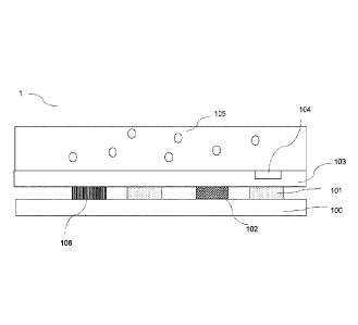
Fig. 1 is a schematic side view of a sensor module 1 according to the
invention for multiparametric
analysis of a medium 105. The sensor module 1 has at least one organic light
emitter for emitting
a first photonic signal 101 and at least one device for detecting photonic
signals 102. The organic
light emitter 101 and the device for detecting photonic signals 102 are formed
monolithically on a
semiconductor substrate 100 which is advantageously formed as a CMOS
semiconductor
substrate. Furthermore, the sensor module 1 has at least one functional layer
system 103 which
covers the at least one organic light emitter 101 and/or the at least one
device for detecting
photonic signals 102 and is in contact with the medium 105. The functional
layer system 103 has
at least one active region 104. The sensor module 1 has a component for
determining a second
property by means of a non-photonic measurement principle 106, which component
is arranged
on the semiconductor substrate 100.
Furthermore, the sensor module 1 advantageously has at least one device for
storing data and/or
for evaluating and influencing data and/or for transmitting data and/or for
communication and/or
at least one device for controlling and/or modulating/demodulating the at
least one organic light
emitter and/or the at least one device for detecting photonic signals 107.
Furthermore, the sensor
module 1 advantageously has a device for providing the electrical energy 108
to be used for
operating the sensor module 1.
Fig. 2 is a schematic side view of an embodiment of the sensor module 1
according to the
invention for multiparametric analysis of a medium 105. The sensor module 1
corresponds to the
sensor module from Fig. 1, The functional layer system 103 has a functional
layer carrier 103.1
and a functional layer 103.2. The functional layer carrier 103.1 can be
designed as an optical lens
or as an optical lens array or as an optical filter or as an optical grating
or as a combination of the
aforementioned.
Date Recue/Date Received 2021-12-23
CA 03145141 2021-12-23
17
Fig. 3 shows schematically a sensor module 1 in a fermentation reactor 2 which
is filled with a
medium 105. The sensor module 1 corresponds to the sensor module 1 shown in
Fig. 1. It can
be seen that the functional layer system 103 is in contact with the medium 105
and shields the
organic light emitter 101 and the device for detecting photonic signals 102
from the medium 105.
The sensor module 1 has at least one device for storing data and/or for
evaluating and influencing
data and/or for transmitting data and/or for communication 107. Furthermore,
the sensor
module 1 can have at least one device for controlling and/or
modulating/demodulating the at least
one organic light emitter and/or the at least one device for detecting
photonic signals (not shown).
The sensor module 1 can furthermore have a device for providing the electrical
energy to be used
for operating the sensor module (not shown).
Date Recue/Date Received 2021-12-23
CA 03145141 2021-12-23
18
List of reference signs
1 Sensor module
100 Semiconductor substrate
101 Organic light emitter
102 Device for the detection of photonic signals
103 Functional layer system
103.1 Functional layer carrier
103.2 Functional layer
104 Active region
105 Medium
106 Component for determining at least one second property
107 Device for storing data and/or for evaluating and influencing
data
and/or for transmitting data and/or for communication
2 Fermentation reactor
Date Recue/Date Received 2021-12-23
CA 03145141 2021-12-23
19
Cited non-patent literature
[Krujatz2016] Krujatz F. et al "Exploiting the Potential of OLED-Based Photo-
Organic Sensors
for Biotechnological Applications"; Chem Sci J 2016 Vol. 7, Issue 3, 1000134,
DOI: 10.4172/2150-3494.1000134
Date Recue/Date Received 2021-12-23