Note: Descriptions are shown in the official language in which they were submitted.
CA 03146188 2022-01-06
WO 2021/003581 PCT/CA2020/050961
1
BLOCKCHAIN MICROPROCESSOR AND METHOD
RELATED
[0001] This application claims priority to U.S. Prov. App. No. 62/872,914,
filed on July 11,
2019, the contents of which are explicitly incorporated by reference herein in
its entirety.
FIELD
[0002] This invention relates to methods and devices of blockchain technology,
and more
specifically to blockchain microprocessors and methods for data storage,
transfer and sharing
between devices.
BACKGROUND
[0003] The current use of Block chain technology focuses mainly on the use of
the general
ledger to record ownership of non-fungible tokens mainly used to document
financial
transactions along with the derivative products, including, but not limited to
loans, interest
payments, collateral, debt obligations, and in some cases real-world assets
including medical
history, personal identification data, physical art, music, or real estate.
[0004] Blockchain technology can be defined as a record of data and data
transactions between
two or more unrelated parties typically referred to as a general ledger.
Typically, all participants
in the blockchain have identical copies of the general ledger. Another
defining feature of the
blockchain is the consensus protocol used to verify the validity and integrity
of the data being
written to the general ledger.
CA 03146188 2022-01-06
WO 2021/003581 PCT/CA2020/050961
2
SUMMARY
[0005] Any and all aspects as described herein, individually and/or in any
combination
consistent to the understanding of one of skill in the art upon review of the
present application.
[0006] According to an aspect herein, there is provided a blockchain
microprocessor core for a
blockchain. The blockchain microprocessor core may have a primary memory for
storing one or
more instructions therein; a control processor may execute one or more of the
instructions; an
arithmetic-logic processor may execute one or more of the instructions. The
blockchain
microprocessor core may have one or more registers; a blockchain general
ledger; a blockchain
memory; and one or more input/output (TO) ports. The registers may have a
blockchain
instruction register, a blockchain address register, a blockchain buffer
register, and a blockchain
program counter.
[0007] The instructions may have an initiation protocol. The initiation
protocol may: establish a
data stream over the at least one TO port; verify the data stream over the at
least one TO port; and
establish one or more data transfer protocols between the control processor
and a receiving
device via the at least one TO port. The receiving device may be selected from
one or more of:
another blockchain microprocessor core, a server, a blockchain validator, an
Internet Protocol
address, a MAC address, a DNS address, a blockchain miner, a blockchain node,
a data router,
an Internet-of-Things device, and a blockchain-of-things device. The data
transfer protocols may
establish a security protocol, a routing table, and a consensus protocol. The
consensus protocol
may have one or more of a proof-of-work and a proof-of-stake.
[0008] The instructions may determine one or more node parameters for a secure
functioning
and validation of the blockchain. The node parameters may be selected from one
or more of: a
CA 03146188 2022-01-06
WO 2021/003581 PCT/CA2020/050961
3
speed of block verification, a duration for the blockchain, and an
availability of computing power
within an accessible sphere of influence.
[0009] According to another aspect, there is provided a processor for a
blockchain. The
processor may have a plurality of blockchain microprocessor cores; a bus
interface; at least one
Li blockchain cache associated with each of the plurality of blockchain
microprocessor cores; at
least one L2 cache shared between the plurality of blockchain microprocessor
cores. The
processor may have a blockchain memory storing a plurality of instructions.
The blockchain
memory may have one or more of: a blockchain random access memory (B-RAM), a
blockchain
read-only memory (B-ROM), a blockchain basic input output system (B-BIOS), and
a
blockchain general ledger. The one or more blockchain microprocessor cores may
execute a
heartbeat protocol for the blockchain.
[0010] The B-BIOS may have the instructions to perform a boot cycle comprising
at least one
reference instruction, a data, and a logic received from the blockchain. The B-
BIOS may have
the instructions to establish a connection to the blockchain. The B-BIOS may
have the
instructions to manage at least one data flow between the plurality of
blockchain processor cores
and the blockchain. The B-BIOS may fetch the instructions from the B-ROM.
[0011] The processor may further have one or more general central processing
unit cores in
communication with the plurality of blockchain microprocessor cores over the
bus interface.
CA 03146188 2022-01-06
WO 2021/003581 PCT/CA2020/050961
4
DESCRIPTION OF THE DRAWINGS
[0012] While the invention is claimed in the concluding portions hereof,
example embodiments
are provided in the accompanying detailed description which may be best
understood in
conjunction with the accompanying diagrams, and where:
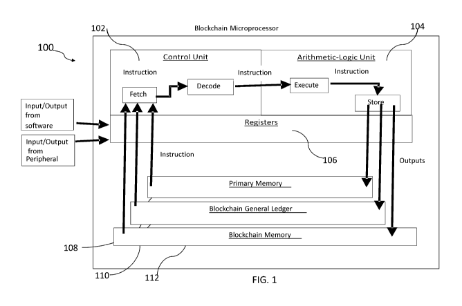
[0013] Figure 1 is a block diagram of a blockchain microprocessor;
[0014] Figure 2 is a block diagram of another blockchain microprocessor;
[0015] Figure 3 a block diagram of a blockchain microprocessor according to a
further aspect;
and
[0016] Figure 4 is a block diagram of a blockchain microprocessor according to
another aspect.
DETAILED DESCRIPTION
[0017] Blockchain technology is designed by nature to be trustless, meaning
little to no trust
may be required between participants for a blockchain to function as intended.
Every increase in
distance between an electrical signal and the blockchain requires trust in an
automatic or manual
process. As shown in FIG. 1, a blockchain microprocessor 100 according to one
aspect
described herein provides a shortest distance between the electrical signal
and a circuit or device
capable of writing, and/or reading, data to, and/or from, the blockchain
directly or through an
intermediary.
[0018] Previously, blockchain technology refers to the blockchain used as a
means of storing
information or data, known as a general ledger, or a means of executing pieces
of computer code,
known as a smart contract. The blockchain as described herein may provide a
means of data
CA 03146188 2022-01-06
WO 2021/003581 PCT/CA2020/050961
communication (e.g. transmission and reception) between one or more
independent electronic
units, such as, for example, separate portions of a circuit board, separate
computing machines, or
separate blockchains. The blockchain technology described herein may enable a
form of
computer programming in which the data communication occurs via the
blockchain.
5 [0019] Another aspect described herein applies the blockchain technology
to a data transfer
between one or more computing devices, specifically by providing a dedicated,
purpose-built
microprocessor 100. This microprocessor 100 may either soldered into the
circuit board,
inserted onto the circuit board as a peripheral, or may function as a
standalone computing device
with a dedicated circuit board, and is wired such that the microprocessor 100
receives at least the
same inputs, if not more, as a main processor or other data stream as
applicable. The
microprocessor 100 may also receive data from the main processor but may
operate without
control from the main processor and/or any other portion of the circuit board
other than power
from a power supply. The blockchain microprocessor 100 may also send control
signals to the
main processor and/or any other portion of the circuit board.
[0020] Using the blockchain for data transfer between the one or more circuits
and/or computing
devices enables these devices to conduct one or more operations in a shared
environment similar
to a shared "reality". This shared reality may be analogous to living
organisms sharing a reality
through sensory inputs of sight, touch, smell, taste, and so on. Prior
computing devices were
typically provided with a permissioned reality in which to operate. These
permissioned realities
constrain the input sources of the computing devices, which may be limited by
space, sensor
data, time, and/or permission to access centralized databases and/or memory.
The shared reality
may be a useful function of the general ledger as created by blockchain
technology since the
shared reality provides access to all computing devices sharing the blockchain
to have a more
CA 03146188 2022-01-06
WO 2021/003581 PCT/CA2020/050961
6
complete permission to data, and may interact better with, the physical or
digital environment
without constraint while equally prohibiting unauthorized modification.
[0021] An example of blockchain technology applications is to determine or
track carbon
emission, such as those disclosed in US Provisional Application Serial No.
62/726, 859, entitled:
"System And Method For Incorporating Sensor Measurements Into A Blockchain",
filed on
September 4, 2018, the disclosure of which is incorporated by reference.
[0022] With reference to FIG. 1, a blockchain microprocessor 100 may be
provided comprising
a control unit 102, an arithmetic-logic unit 104, and/or registers 106. The
microprocessor 100
may also have a primary memory 108, a blockchain general ledger 110, and/or a
blockchain
.. memory 112. The registers 106 may include dedicated specialized registers,
such as i)
Blockchain Instruction Register, ii) Blockchain address Register, iii)
Blockchain Buffer Register
and/or iv) Blockchain Program Counter.
[0023] The general functions provided by the blockchain microprocessor 100 may
include a
number of functions as described herein. During initialization of the
microprocessor 100, an
.. initialization function may engage in an initiation protocol where the
protocol has three distinct
functions: (1) Establishing and verifying an incoming data stream from the
circuit board; (2)
Establishing one or more data transfer protocols between the microprocessor
100 and the other
aspects of the circuit board, and (3) Establishing the data transfer protocol
between the
microprocessor 100 and a receiving device. This receiving device may be
another blockchain
microprocessor device 100, a server, a blockchain validator, an Internet
Protocol address, a MAC
address, a DNS address, a blockchain miner, a blockchain node, a data router,
and/or any other
CA 03146188 2022-01-06
WO 2021/003581 PCT/CA2020/050961
7
Internet-of-Things device and/or blockchain-of-things device with the capacity
to receive,
process, and send data.
[0024] The outward-facing data transfer protocol establishment (e.g.
handshake) may enable the
microprocessor 100 to establish combinations of one or more data transfer
protocols that may be
used for the data transfer. The protocol establishment may specify any
security protocols
required, routing tables for a specific route the data transfer may take
between the one or more
devices, and one or more details of the establishment, structuring,
transferring, securing, and/or
termination of the blockchain data. The handshake may also establish which
consensus protocol
the blockchain microprocessors 100 may use, including but not limited to,
proof-of-work or
proof-of-stake. This outward facing data transfer protocol establishment may
be broadcast by
one or all of the following: Wi-Fi signal, Peer-to-peer communication,
Blockchain
communications protocol, sound frequencies (auditory and/or ultrasonic),
Microwave
frequencies, Power Line communications, TCP/IP, and/or any other
communications protocol or
technique.
[0025] One or more functions of the blockchain microprocessor 100 may include
control of the
blockchain microprocessor 100, read/write, and communications functions of the
circuit board.
The blockchain microprocessor 100 can also serve as either a slave, a master,
or an equal to the
main processor or any other function of the circuit board or machine. The
blockchain
microprocessor 100 may send and receive instructions to and/or from third
parties' devices,
peripherals, and/or inter-machine functions. The blockchain microprocessor 100
may use
shared, or dedicated resources, within the computing machine and circuit board
including short-
and long-term memories (e.g. random access memory (RAM), read-only memory
(ROM), hard
disk, Flash memory, etc.).
CA 03146188 2022-01-06
WO 2021/003581 PCT/CA2020/050961
8
[0026] Multiple blockchain microprocessors 100 on the same circuit board
and/or between
separate circuit boards or computing devices may share resources and/or
coordinate operations.
One such example may be in swarm-type computing devices where the blockchain
microprocessor 100 may coordinate cooperation and sharing of resources within
the swarm. The
swarm may dedicate a portion of the computing resources to an operation of an
individual circuit
board and dedicate another portion of the circuit board's resources to the
shared goal of the
successful operation of the blockchain. The allocation of resources may be
static or dynamically
performed (either asynchronously or synchronously).
[0027] The blockchain microprocessor 100 may transmit data including, but not
limited to logic,
.. algorithms, and/or mathematical operations, from one blockchain
microprocessor to another
blockchain processor independent of a source.
[0028] The blockchain microprocessor 100 may be programmed with firmware at a
time of
manufacture and may be capable of incorporating algorithms from other
blockchain processors
100. The blockchain microprocessor 100 may design algorithms as an evolution
of operations
.. and/or from sharing at least a portion of an algorithm from other
blockchain microprocessors.
The blockchain microprocessor 100 may also obtain one or more algorithms from
any other
sources of data.
[0029] The blockchain microprocessor 100 may determine which data is stored
in, and retrieved
from, short-term and long-term memory. The data storage memory may be
physically located
adjacent to (or within) the blockchain microprocessor 100 on a circuit board.
The data storage
memory may be located remotely such as in the cloud, or on a separate
computing device which
is in blockchain communication with the microprocessor 100, or in a purpose
built blockchain
data center on the circuit board. By storing blockchain data in a purpose
build memory data
CA 03146188 2022-01-06
WO 2021/003581 PCT/CA2020/050961
9
center, the resources of the other processors on the circuit board may be
freed from having to
maintain the integrity of the blockchain and permit the other processors to
perform the other
functions of the circuit board.
[0030] The logic of the microprocessor 100 may determine content of a genesis
block of the
blockchain along with any other aspects of the blockchain's nature and
operation.
[0031] The blockchain microprocessor 100 may dedicate and/or coordinate
computing power
from the blockchain microprocessor 100, the main processor, and/or any other
aspect of the
circuit board, to a hash rate and/or operations to maintain proper operation
of the blockchain.
[0032] The blockchain microprocessor 100 may fetch commands from the
blockchain in
addition to memory and registry sources located on the circuit board. The
blockchain processor
may execute logic from data contained on the blockchain.
[0033] The blockchain microprocessor 100 may determine a size and a number of
one or more
nodes required in a network for a secure functioning and validation of the
blockchain and may
make connections with those other validators. The size and the number may be
determined by
parameters including but not limited to a speed of block verification, a
duration the blockchain is
expected to be used for, an availability of spare computing power within a
sphere of influence to
which the blockchain microprocessor has access.
[0034] The blockchain microprocessor 100 may establish one or more necessary
parameters, and
may perform one or more necessary steps, for a consensus protocol to be used
in the blockchain.
[0035] According to one aspect, the blockchain microprocessor 100 may be
constructed with
additional blockchain microprocessors 100 in order to have a dual-core
blockchain
microprocessor. For example, FIG. 2 illustrates a dual-core blockchain
microprocessor 200
CA 03146188 2022-01-06
WO 2021/003581 PCT/CA2020/050961
having a first sub-blockchain microprocessor 202 and a second sub-blockchain
microprocessor
204.
[0036] According to another aspect, the blockchain microprocessor 100 may be a
dual-core
hybrid microprocessor 300 having a general-purpose CPU core 302 and a
blockchain
5 microprocessor 100. FIG. 3 illustrates a blockchain microprocessor 300
having a CPU core 302
and a sub-blockchain microprocessor 304.
[0037] According to further aspect, the blockchain processer 100 may comprise
dual-processors
embedded within a multi-core processor. As shown in FIG. 4, the blockchain
processer 400
includes a dual blockchain microprocessor having a sub-blockchain
microprocessor 402a and a
10 sub-blockchain microprocessor 402b, and dual-core general-purpose
processor including
microprocessor 404a and microprocessor 404b.
[0038] The blockchain microprocessor 100 may include a dedicated RAM and/or a
dedicated
ROM having capacities independent of a system RAM and a system ROM. For
example, the
blockchain microprocessor 400 may have Blockchain RAM (B-RAM) and Blockchain
ROM (B-
ROM) 406. The B-RAM may be used to store incoming data and/or logic from the
blockchain
and the B-ROM may be used to store data and/or logic on a more permanent basis
(e.g. after
power has been removed from the processor). The blockchain microprocessor 100
may have
authority over the B-RAM and the B-ROM. ROM is used herein to not exclusively
be read-only
but may be modified. The intended use of ROM herein is to imply that the data
and/or
instructions stored therein are maintained once power has been removed.
[0039] According to a further aspect, a blockchain microprocessor 100 may also
comprise a
Blockchain Basic Input Output System (B-BIOS), as shown in FIG. 4. The B-BIOS
may have
CA 03146188 2022-01-06
WO 2021/003581 PCT/CA2020/050961
11
the instructions referenced during a boot cycle to reference instructions,
data, or logic, received
from the blockchain, or to establish the connection to the blockchain upon
circuit boot up. The
B-BIOS may manage one or more data flows between the device and the blockchain
and/or any
peripherals that may be connected to the device. The B-BIOS tests system
hardware on the
computing device on startup. The B-BIOS may then fetch any instructions in the
B-ROM called
the Blockchain Boot Sector (B-BOOT). This B-BOOT sector program may execute
instructions
that help to utilize the computing device effectively and/or enable the
blockchain functionality to
operate properly.
[0040] In blockchain communications, a problem may be encountered known as
"split-brain"
problem. The split-brain problem refers to data or availability
inconsistencies resulting from
maintenance and operation of two or more separate data sets or communication
protocols (e.g.
DNS) that overlap in scope. The split-brain problem occurs when the data sets
do not
communicate and synchronize properly. The split-brain problem may cause data
corruption,
and/or data loss, as the newly split portions of the communications protocols,
and/or data sets,
both claim each are correct and continue to function independently of each
other.
[0041] A solution to the split-brain problem may be an agreed upon heartbeat
protocol, which
functions to synchronize the two or more sides of the data, and/or
communications streams. The
heartbeat protocol operates on a First-in First-out basis to handle the data
streams throughout the
network. As part of the heartbeat protocol the respective nodes may send a
response indicating
the node remains active and continues to function in a coordinated manner.
[0042] According to one aspect, the blockchain microprocessor 100 may operate
the heartbeat
protocol to provide other computing devices an indication that the blockchain
microprocessor
CA 03146188 2022-01-06
WO 2021/003581 PCT/CA2020/050961
12
100 is operational. The heartbeat protocol may be synchronized and maintained
by the
blockchain microprocessor 100. The blockchain microprocessor 100 may ensure
sufficient
numbers of network links that serve as additional heartbeat channels to the
CPU in order to
prevent this split-brain problem. The blockchain microprocessor 100 may be
used for automation
.. of a quorum-consensus approach to resolve any conflict between one or more
nodes.
[0043] According to another aspect, the blockchain microprocessor 100 may be
manufactured as
a standalone microprocessor on a circuit board, or as part of a multi-core
processor, such as the
multi-core processor 400 shown in FIG. 4. Multi-core processors are also
intended to refer to
digital signal processors (DSP) and system on a chip (SoC). Where parallel
operations is
intended to refer to systems that run in parallel to a blockchain operation,
use the read/write
functions of the blockchain, or run as a program that uses both the blockchain
and one or more
microprocessors as shown in FIG. 4.
[0044] In another aspect, the blockchain microprocessor may be designed as a
OSI-compatible
device as per the following ISO standards; ISO/IEC 7498-1 The Basic Model, ISO
7498-2
Security Architecture, ISO/IEC 7498-3 Naming and addressing, and ISO/IEC 7498-
4
Management framework, or any other standard or programming language used in
signal
processing, and networking protocols.
[0045] In some aspects, the blockchain microprocessor 100 may operate with a
shared cache
alongside other microprocessors, or be designed with a dedicated cache,
including but not
.. limited to a blockchain-BIOS which may be designed as electrically-erasable
programmable
ROM chip, a blockchain-RAM and a blockchain ROM. These may be considered
additional
registers on the chip.
CA 03146188 2022-01-06
WO 2021/003581 PCT/CA2020/050961
13
[0046] The foregoing is considered as illustrative only of the principles of
the invention.
Further, since numerous changes and modifications will readily occur to those
skilled in the art,
it is not desired to limit the invention to the exact construction and
operation shown and
described, and accordingly, all such suitable changes or modifications in
structure or operation
which may be resorted to are intended to fall within the scope of the claimed
invention.