Note: Descriptions are shown in the official language in which they were submitted.
WO 2020/236129
PCT/US2019/018453
TITLE OF INVENTION:
Packaging Technique for Inductive Conductivity Sensors
CROSS-REFERENCE TO RELATED APPLICATIONS: Co-pending US utility patent
application
14/721,444, "Conductivity and Impedance Sensor", by the same inventor.
BACKGROUND OF THE INVENTION:
Inductive conductivity sensors are widely used in quality monitoring and
process control for
many industrial and research applications. Non-contact, inductive conductivity
sensors are
of interest because of their immunity to chemical corrosion and maintaining
their
calibration for a longer period of time. The manufacturing process of
conventional inductive
conductivity sensors requires complicated, time-consuming, and expensive
production
steps. While the fundamental measurement concept is simple, the main
complexity of the
conductivity sensor comes from its packaging process.
This invention presents a new packaging technique that allows for the use of a
wider range
of isolating materials for inductive conductivity sensors, which will
significantly reduce the
cost of producing the sensor and increase its sensitivity. It will combine
exceptionally
advantageously with the conductivity and impedance sensors that are the
subject of this
inventor's co-pending application number 14/721,444, and the disclosure of
that
application is incorporated herein be reference.
1
CA 03146695 2022-2-2
WO 2020/236129
PCT/US2019/018453
BRIEF SUMMARY OF THE INVENTION:
The polymers employed to isolate the magnetic cores, and the materials used to
protect
them against the under-test substance, affect the electrical and magnetic
properties of the
sensor. In order to overcome this issue, in conventional sensors, the
components of the
magnetic system are separated from the polymer material using a secondary
material such
as a porous ceramic cement. A very limited group of materials with unique
properties can
be used for this purpose. The process and material expenses for the secondary
material
add a significant cost to the manufacturing process of the sensor.
Furthermore, the
secondary material affects the performance of the sensor. A limited group of
materials can
be used for the secondary isolation due to their required chemical,
mechanical, electrical,
and magnetic properties. Often, a third material such as a metal support is
also required to
mechanically protect the sensitive secondary insulator from external
mechanical tensions.
This invention presents a new packaging technique that allows for the use of a
wider range
of isolating materials for inductive conductivity sensors. It will
significantly reduce the cost
of producing the sensor, improve its precision and accuracy, and increase its
sensitivity.
BRIEF DESCRIPTION OF THE SEVERAL VIEWS OF THE DRAWING:
FIG. 1A, Prior Art, illustrates the simplest form of the toroidal conductivity
sensor
comprising a drive toroid, a receiving toroid, and a conductive material
around the sensor
making a current loop that transfers the energy from the driving toroid to the
sensing
toroid_ FIG. 1B, Prior Art, illustrates the cross-section view of the simplest
form of the
toroidal conductivity sensor. This figure shows how a non-conductive,
magnetically
2
CA 03146695 2022-2-2
WO 2020/236129
PCT/US2019/018453
transparent material such as a corrosion-resistive polymer is employed to
protect the
magnetic core and wires from the under-test substance.
FIG. 2A, Prior Art, illustrates a shielding disk placed between two toroids
preventing direct
induction from the drive toroid to the sensing toroid_ FIG. 2B shows the
embodiment of a
conventional toroidal conductivity measurement sensor. The sensor comprises a
driving
toroid, a sensing toroid, a shielding conductive disk, a corrosion-resistive
polymer, a
secondary insulating material, and metal casing.
FIG. 3, Prior Art, shows how the secondary insulating material makes a closed
loop around
the drive toroid and the sensing toroid, causing a current loop due to any
electrical or
magnetic conductivity of the material, resulting a transfer of energy from the
drive toroid to
the sensing toroid.
FIG. 4 shows the embodiment of this novel packaging for a toroidal
conductivity-
measurement sensor.
FIGS. 5A and 56 show the embodiment of this novel packaging for toroidal
conductivity-
measurement sensors with 3 toroids. FIG. 5A shows an embodiment with two
driving
toroids and one receiving toroid, and FIG. 56 shows an embodiment with one
driving toroid
and two receiving toroids.
DETAILED DESCRIPTION OF THE INVENTION:
The simplest form of the toroidal conductivity sensor in prior art is
illustrated in FIG. 1A.
The sensor is comprised of a drive toroid 101 and a receiving or sensing
toroid 102. A
conductive material around the sensor makes a current loop 103 that transfers
the applied
3
CA 03146695 2022-2-2
WO 2020/236129
PCT/US2019/018453
energy from driving toroid 101 to sensing toroid 102. The electrical
parameters of this
measurement structure, when surrounded by the under-test substance, are
affected due to
electrical and magnetic properties of the under-test substance. As introduced
in the prior
art and as shown in FIG. 18, a non-conductive, magnetically transparent
material 104, often
a corrosion resistive polymer, is employed to protect the magnetic core and
wires from the
under-test substance. The insulator 104 can also mechanically stabilize the
sensor. The
main problem of the sensor embodiment of FIG. 1B is the direct induction from
the drive
toroid 101 to the sensing toroid 102. To prevent the direct induction that
affects the
sensor's functionalities, as illustrated in FIG. 2A, a shielding disk 105 is
placed between the
two toroids. The shielding material 105 can be metal or any conductive
material. It is also
common to ground the shielding material 105.
It is known that the sensor embodiment of FIG. 18 or FIG. 2A is affected by
the dielectric
properties of the under-test substance. The corrosion-resistive polymer 104 is
often a good
dielectric material. Material 104, in combination with the under-test
substance, affects the
self-capacitance of the wires of the drive toroid 101 and the self-capacitance
of the wires of
the receiving toroid 102 and the mutual capacitance made between the wires of
two
toroids. The common technique to reduce the influence of the dielectric
properties of the
under-test material on the self-capacitance and mutual capacitance of the
toroids is the use
of a secondary insulating material 108. The insulating material 108 has a weak
dielectric
property or it has a spongy or porous structure that results a low equivalent
capacitance.
Materials that satisfy the criteria for insulator 108 can be brittle or
sensitive to mechanical
shocks. Hence, it is very common to employ a mechanically-stronger metallic
casing to
protect the insulator 108. The metal casing 106 also acts as a shielding cage
to protect the
4
CA 03146695 2022-2-2
WO 2020/236129
PCT/US2019/018453
sensor from external electromagnetic noises. It is also common to ground the
metal casing
106 to improve its shielding properties. A gap 107, which can be an air-gap or
filled with any
non-conducting material, should prevent the metal casing 106 from making a
closed loop as
a conductor around either the drive toroid or the sensing toroid or both
toroids. The
embodiment of the conventional sensors is shown in FIG. 2B.
As shown in FIG. 3, material 108 makes a closed loop 109 around toroid 101 and
toroid 102.
Any electrical or magnetic conductivity of the material 108 results in a
transfer of energy
from the drive toroid 101 to the sensing toroid 102. A direct transfer of
energy via loop 109
results in an error in the conductivity measurement. Considering this fact, it
is obvious that
a very limited group of materials can be used as material 108 in the sensor
embodiment,
because of their necessarily unusual electrical, magnetic, and dielectric
properties. Material
108 should have four major properties: poor capacitance, high magnetic
transparency, high
magnetic reluctance, and low electrical conductivity. Any degradation of
material 108 over
time can affect at least one of these four properties and result in a
significant decline in the
sensor's accuracy.
This invention presents a new structure that eliminates the dependence of the
sensor on a
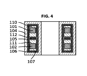
practically unique material 108. In this novel technique, as shown in Fig. 4,
a magnetically
transparent, non-electrically conductive material 112 is employed to separate
the toroids.
The toroid 101 and the material 110 around toroid 101 are separated from
toroid 102 and
the material 111 around toroid 102 using a shielding material 112. Material
110 and
material 111 have poor capacitance and are magnetically transparent. This
innovative
invention allows the use of a wider range of substances as materials 110 and
111, including
CA 03146695 2022-2-2
WO 2020/236129
PCT/US2019/018453
a wider group of ceramic compounds with better mechanical properties that do
not require
a metal structure for mechanical protection. This includes, but is not limited
to, any porous
cements and spongy polymers and foams. Preventing a closed loop of material
110 or
material 111 around both toroids (similar to loop 109 in Fig. 3) in the new
embodiment
significantly reduces the measurement error. Avoiding a metallic casing 106,
or reducing its
thickness, results better sensitivity in conductivity measurement. The
simplest embodiment
for this invention is shown in FIG. 4. The sensor embodiment of FIG. 4 also
includes an
optional thin conductive layer 106 for shielding purposes. This conductive
layer includes a
gap 107 that can be an air-gap or filled with any non-conducting material. The
gap 107
prevents the conductive layer 106 from making a conductive closed loop around
either
drive toroid 101, or sensing toroid 102, or both toroids. The conductive layer
106 can be
grounded to improve its shielding properties. As shown in FIG. 4 the preferred
embodiment
for the sensor also comprises a shielding disk 105 that prevents the direct
transfer of
energy from toroid 101 to toroid 102. The shielding disk 105 can also be
grounded to
improve its shielding properties.
The idea of using a magnetically transparent, non-electrically conductive
material 112 to
separate the driving toroid from the receiving toroid, and using two separate
magnetically
transparent materials 110 and 111 with poor capacitance around the toroids,
can also be
used for inductive conductivity sensors with 3 toroids. Conductivity sensors
with three
toroids are commonly used to achieve a higher precision and higher accuracy
measurement. A sensor structure with one driving toroid and two receiving
toroids
(connected in series) is commonly used to achieve higher sensitivity, and a
sensor structure
6
CA 03146695 2022-2-2
WO 2020/236129
PCT/US2019/018453
with two driving toroids (connected in series) and one receiving toroid is
known to be less
sensitive to external noise.
In the sensor embodiment shown in FIG. SA, the sensor comprises two drive
toroids, 101
and 113, and one sensing toroid 102. Electromagnetically transparent
components 110,
111, and 114, which have poor capacitance properties, surround the three
toroids, and the
toroids are separated from each other using insulator 112. This embodiment can
also be
practiced using one driving toroid and two receiving toroids as shown in FIG.
SB. In FIG. SB
the sensor comprises one drive toroid 101 and two sensing toroids 102 and 115.
Electromagnetically transparent components 110, 111, and 116, which have poor
capacitance properties, surround the three toroids, and the toroids are
separated from
each other using insulator 112.
7
CA 03146695 2022-2-2