Note: Descriptions are shown in the official language in which they were submitted.
CA 03147123 2022-01-12
WO 2021/007680
PCT/CA2020/050995
MULTI-PHASE WIRELESS ELECTRIC FIELD POWER TRANSFER SYSTEM,
TRANSMITTER AND RECEIVER
Related Application
This application claims the benefit of U.S. Provisional Application No.
62/875,043
filed on July 17, 2019, the entire content of which is incorporated herein by
reference.
Field
[0001] The subject disclosure relates generally to wireless power transfer
and in particular, to
a wireless electric field power transfer system, and to a transmitter and
receiver therefor.
Back2round
[0002] A variety of wireless power transfer systems are known. A typical
wireless power
transfer system includes a power source electrically connected to a wireless
power transmitter,
and a wireless power receiver electrically connected to a load. In magnetic
induction systems,
the transmitter has an inductor that transfers electrical energy from the
power source to an
inductor of the receiver. Power transfer occurs due to coupling of magnetic
fields between the
inductors of the transmitter and receiver. The range of these magnetic
induction systems is
limited and the inductors of the transmitter and receiver must be in optimal
alignment for
effective power transfer. There also exist resonant magnetic systems in which
power is
transferred due to coupling of magnetic fields between the inductors of the
transmitter and
receiver. However, in resonant magnetic systems the inductors are resonated
using at least one
capacitor. The range of power transfer in resonant magnetic systems is
increased over that of
magnetic induction systems and alignment issues are rectified. While
electromagnetic energy is
produced in magnetic induction and resonant magnetic systems, the majority of
power transfer
occurs via the magnetic field. Little, if any, power is transferred via
electric induction or
resonant electric induction.
[0003] In electrical induction systems, the transmitter and receiver have
capacitive
electrodes. Power transfer occurs due to coupling of electric fields between
the capacitive
electrodes of the transmitter and receiver. Similar, to resonant magnetic
systems, there exist
resonant electric systems in which the capacitive electrodes of the
transmitter and receiver are
1
CA 03147123 2022-01-12
WO 2021/007680 PCT/CA2020/050995
made resonant using at least one inductor. Resonant electric systems have an
increased range of
power transfer compared to electric induction systems and alignment issues are
rectified. While
electromagnetic energy is produced in electric induction and resonant electric
systems, the
majority of power transfer occurs via the electric field. Little, if any,
power is transferred via
magnetic induction or resonant magnetic induction.
[0004] Although wireless power transfer techniques are known, improvements
are desired.
It is therefore an object to provide a novel wireless electric field power
transfer system, a
transmitter and receiver therefor and a method of wirelessly transmitting
power.
Summary
[0005] It should be appreciated that this Summary is provided to introduce
a selection of
concepts in a simplified form that are further described below in the Detailed
Description of
Embodiments. This Summary is not intended to be used to limit the scope of the
claimed subject
matter.
[0006] Accordingly, in one aspect, there is provided a transmitter
comprising: a multi-phase
radio-frequency (RF) converter configured to output multiple sinusoidal RF
power signals; and a
multi-phase resonator configured to receive the multiple sinusoidal RF power
signals and
resonate multiple inductors and capacitive electrodes at a resonant frequency
at multiple phases
to transfer power via resonant electric field coupling.
[0007] In one or more embodiments, the capacitive electrodes are multi-fold
rotationally
symmetric. In one or more embodiments, an axis of the multi-fold rotational
symmetry is
normal to a major face of the capacitive electrodes about a centre of
curvature of the capacitive
electrodes.
[0008] In one or more embodiments, the multi-phase RF converter comprises a
multi-phase
RF inverter comprising multiple transistors, each transistor electrically
connected to an inductor
of the multi-phase transmit resonator.
[0009] In one or more embodiments, the transmitter further comprises a
power source
electrically connected to the multi-phase RF converter, wherein the power
source is configured
to output a direct current (DC) power signal.
[0010] In one or more embodiments, the multi-phase transmit resonator is
balanced.
[0011] In one or more embodiments, the multi-phase transmit resonator
comprises three
inductors and three capacitive electrodes.
2
CA 03147123 2022-01-12
WO 2021/007680
PCT/CA2020/050995
[0012] In another aspect, there is provided a receiver comprising: a multi-
phase resonator
comprising multiple inductors and capacitive electrodes configured to resonate
at a resonant
frequency to extract power via resonant electric field coupling and output
multiple sinusoidal
radio-frequency (RF) power signals, wherein the multiple inductors and
capacitive electrodes
resonate at multiple phases; and a multi-phase rectifier configured to receive
the multiple
sinusoidal RF power signals and output a direct current (DC) power signal.
[0013] In one or more embodiments, the capacitive electrodes are multi-fold
rotationally
symmetric. In one or more embodiments, an axis of the multi-fold rotational
symmetry is
normal to a major face of the capacitive electrodes about a centre of
curvature of the capacitive
electrodes.
[0014] In one or more embodiments, the multi-phase rectifier comprises
multiple pairs of
diodes, each pair of diodes electrically connected to an inductor of the multi-
phase receive
resonator.
[0015] In one or more embodiments, the receiver further comprises a load
configured to
receive the DC power signal output by the multi-phase rectifier.
[0016] In one or more embodiments, the multi-phase receive resonator is
balanced.
[0017] In one or more embodiments, the multi-phase receive resonator
comprises three
inductors and three capacitive electrodes.
[0018] In another aspect, there is provided a system comprising: a
transmitter comprising: a
multi-phase radio-frequency (RF) converter configured to output multiple
sinusoidal RF power
signals; and a multi-phase transmit resonator configured to receive the
multiple sinusoidal RF
power signals and resonate multiple transmit inductors and transmit capacitive
electrodes at a
resonant frequency at multiple phases to transfer power via resonant electric
field coupling; and a
receiver comprising: a multi-phase receive resonator comprising multiple
receive inductors and
receive capacitive electrodes configured to resonate at the resonant frequency
to extract power
via resonant electric field coupling and output the multiple sinusoidal RF
power signals, wherein
the multiple receive inductors and receive capacitive electrodes resonate at
the multiple phases;
and a multi-phase rectifier configured to receive the multiple sinusoidal RF
power signals and
output a direct current (DC) power signal.
[0019] In one or more embodiments, the transmit capacitive electrodes are
multi-fold
rotationally symmetric. In one or more embodiments, an axis of the multi-fold
rotational
3
CA 03147123 2022-01-12
WO 2021/007680
PCT/CA2020/050995
symmetry is normal to a major face of the capacitive electrodes about a centre
of curvature of the
capacitive electrodes.
[0020] In one or more embodiments, the receive capacitive electrodes are
multi-fold
rotationally symmetric. In one or more embodiments, an axis of the multi-fold
rotational
symmetry is normal to a major face of the capacitive electrodes about a centre
of curvature of the
capacitive electrodes.
[0021] In one or more embodiments, the multi-phase RF converter comprises a
multi-phase
RF inverter comprising multiple transistors, each transistor electrically
connected to an inductor
of the multi-phase transmit resonator.
[0022] In one or more embodiments, the transmitter further comprises a
power source
electrically connected to the multi-phase RF converter, wherein the power
source is configured
to output a direct current (DC) power signal.
[0023] In one or more embodiments, the multi-phase transmit resonator is
balanced.
[0024] In one or more embodiments, the multi-phase transmit resonator
comprises three
transmit inductors and three transmit capacitive electrodes.
[0025] In one or more embodiments, the multi-phase rectifier comprises
multiple pairs of
diodes, each pair of diodes electrically connected to an inductor of the multi-
phase receive
resonator.
[0026] In one or more embodiments, the receiver further comprises a load
configured to
receive the DC power signal output by the multi-phase rectifier.
[0027] In one or more embodiments, the multi-phase receive resonator is
balanced.
[0028] In one or more embodiments, the multi-phase receive resonator
comprises three
receive inductors and three receive capacitive electrodes.
[0029] In another aspect, there is provided a method of wirelessly
transmitting power via
electric field coupling, the method comprising: converting, at the multi-phase
radio-frequency
(RF) converter of any one of the described transmitters, an input power signal
into multiple
sinusoidal RF power signals; receiving the multiple sinusoidal RF power
signals at the multi-
phase resonator of the transmitter; resonating a transmit inductor and
capacitive electrode pair of
the multi-phase resonator of the transmitter to generate an electric field;
and extracting power by
the multi-phase RF resonator of any one of the described receivers, the multi-
phase RF resonator
of the receiver positioned within the generated electric field.
4
CA 03147123 2022-01-12
WO 2021/007680
PCT/CA2020/050995
[0030] In one or more embodiments, the method further comprises: outputting
received
sinusoidal RF power signals to the multi-phase rectifier of the receiver; and
rectifying the
received sinusoidal RF power signals to a rectified signal.
[0031] In one or more embodiments, the rectified signal is a direct current
(DC) power
signal.
[0032] In one or more embodiments, the input power signal is a DC power
signal.
[0033] In one or more embodiments, resonating the transmit inductor and
capacitive
electrode pair comprises resonating the pair at a resonant frequency of the
multi-phase resonator
of the transmitter.
[0034] In one or more embodiments, resonating the transmit inductor and
capacitive
electrode pair comprises resonating an ith transmit inductor and capacitive
electrode pair at an (i-
1)*360/n, where n is a number of sinusoidal RF power signals.
[0035] In the described embodiments, exemplary resonant frequencies include
13.56 MHz
and 27.12 MHz.
[0036] In the described embodiments, the electric field coupling may be
strongly (or tightly)
or loosely coupled. Loosely coupled indicates that the electrodes of the
transmitter and receiver
are separated by air, i.e. an air core is present between transmitter and
receiver.
[0037] The various elements of the described embodiments, may be combined
in any number
of ways as would be appreciated by one of skill in the art.
Brief Description of the Drawings
[0038] Embodiments will now be described more fully with reference to the
accompanying
drawings, in which:
[0039] FIG. 1 a block diagram of a wireless power transfer system;
[0040] FIG. 2 is a schematic layout of a wireless resonant electric field
power transfer
system;
[0041] FIG. 3 is a block diagram of a wireless power transfer system in
accordance with an
aspect of the disclosure;
[0042] FIG. 4 is a schematic layout of the wireless power transfer system
of FIG. 3;
[0043] FIG. 5A is a schematic layout of a wireless power transfer system in
accordance with
an aspect of the disclosure;
CA 03147123 2022-01-12
WO 2021/007680
PCT/CA2020/050995
[0044] FIG. 5B is a graph of the load voltage output by the multi-phase
rectifier of the
wireless power transfer system of FIG 5A;
[0045] FIG. 6 is a plan view of the transmit capacitive electrodes of the
wireless power
transfer system of FIG. 5A;
[0046] FIG. 7 is a plan view of another embodiment of the transmit
capacitive electrodes of
the wireless power transfer system of FIG. 5A;
[0047] FIG. 8 is another plan view of the transmit capacitive electrodes of
FIG. 7;
[0048] FIG. 9 is a plan view of another embodiment of the transmit
capacitive electrodes and
receive capacitive electrodes of the wireless power transfer system of FIG.
5A;
[0049] FIG. 10 is a graph of the radio frequency (RF) efficiency of the
wireless power
transfer system of FIG. 5A with the transmit capacitive electrodes and receive
capacitive
electrodes of FIG. 9;
[0050] FIG. 11 is a plan view of another embodiment of the transmit
capacitive electrodes of
the wireless power transfer system of FIG. 5A;
[0051] FIG. 12 is a perspective view of a wireless power transfer system in
accordance with
an aspect of the disclosure;
[0052] FIG. 13 is a graph of the ratio of the sum of currents to the
magnitude of the currents
as a percentage for a rotation from 0 to 120 degrees for the transmit and
receive capacitive
electrodes of the wireless power transfer system of FIG. 12;
[0053] FIG. 14 is a graph of the phase of the current signal on each
receive segment as a
function of angular position of the wireless power transfer system of FIG. 12;
[0054] FIG. 15 is a graph of the radio frequency (RF) efficiency of the
wireless power
transfer system of FIG. 12 as a function of angular rotation;
[0055] FIG. 16 is a graph of the real part of the impedance presented at
each transmit
capacitive electrode of the wireless power transfer system of FIG. 12 as a
function of angular
rotation;
[0056] FIG. 17 is a graph of the imaginary part of the impedance presented
at each transmit
capacitive electrode of the wireless power transfer system of FIG. 12 as a
function of angular
rotation;
6
CA 03147123 2022-01-12
WO 2021/007680
PCT/CA2020/050995
[0057] FIG. 18 is a graph of RF efficiency of the wireless power transfer
system of FIG. 12
and another wireless power transfer system as a function of longitudinal
separation between the
transmit and receive resonators;
[0058] FIG. 19 is a plan view of another embodiment of the transmit
capacitive electrodes of
the wireless power transfer system of FIG. 5A;
[0059] FIG. 20 is a plan view of other embodiments of the transmit
capacitive electrodes of
FIG. 19;
[0060] FIG. 21 is a perspective view of a wireless power transfer system in
accordance with
an aspect of the disclosure;
[0061] FIGs. 22A to 22E are plan views of other embodiments of the
capacitive electrodes of
the wireless power transfer system of FIG. 4;
[0062] FIGs. 23A to 231 are plan views of other embodiments of the
capacitive electrodes of
the wireless power transfer system of FIG. 5;
[0063] FIG. 24A is a side elevation view of another embodiment of the
capacitive electrodes
of the wireless power transfer system of FIG. 5;
[0064] FIG. 24B is a perspective view of the capacitive electrodes of FIG.
24A;
[0065] FIG. 25A is a side elevation view of the capacitive electrodes of
FIG. 24A forming
transmit and receive capacitive electrodes;
[0066] FIG. 25B is a side elevation view of the capacitive electrodes of
FIG. 24A forming
another embodiment of transmit and receive capacitive electrodes;
[0067] FIG. 26 is a perspective view of another embodiment of the
capacitive electrodes of
the wireless power transfer system of FIG. 5;
[0068] FIG. 27 is a perspective view of another embodiment of the
capacitive electrodes of
the wireless power transfer system of FIG. 5;
[0069] FIG. 28A is a side elevation view of a wireless power transfer
system in accordance
with an aspect of the disclosure;.
[0070] FIG. 28B is a plan view of the wireless power transfer system of
FIG. 28A;
[0071] FIG. 28C is another plan view of the wireless power transfer of FIG.
28A;
[0072] FIG. 29A is a graph of the radio frequency (RF) efficiency of the
wireless power
transfer system of FIG. 29A as a function of angular rotation; and
7
CA 03147123 2022-01-12
WO 2021/007680
PCT/CA2020/050995
[0073] FIG. 29B is a graph of the received rectified voltage of the
wireless power transfer
system of FIG. 29A as a function of angular rotation.
Detailed Description of Embodiments
[0074] The foregoing summary, as well as the following detailed description
of certain
embodiments will be better understood when read in conjunction with the
accompanying
drawings. As will be appreciated, like reference characters are used to refer
to like elements
throughout the description and drawings. As used herein, an element or feature
recited in the
singular and preceded by the word "a" or "an" should be understood as not
necessarily excluding
a plural of the elements or features. Further, references to "one example" or
"one embodiment"
are not intended to be interpreted as excluding the existence of additional
examples or
embodiments that also incorporate the recited elements or features of that one
example or one
embodiment. Moreover, unless explicitly stated to the contrary, examples or
embodiments
"comprising", "having" or "including" an element or feature or a plurality of
elements or features
having a particular property may further include additional elements or
features not having that
particular property. Also, it will be appreciated that the terms "comprises",
"has" and "includes"
mean "including but not limited to" and the terms "comprising", "having" and
"including" have
equivalent meanings.
[0075] As used herein, the term "and/or" can include any and all
combinations of one or
more of the associated listed elements or features.
[0076] It will be understood that when an element or feature is referred to
as being "on",
"attached" to, "connected" to, "coupled" with, "contacting", etc. another
element or feature, that
element or feature can be directly on, attached to, connected to, coupled with
or contacting the
other element or feature or intervening elements may also be present. In
contrast, when an
element or feature is referred to as being, for example, "directly on",
"directly attached" to,
"directly connected" to, "directly coupled" with or "directly contacting"
another element of
feature, there are no intervening elements or features present.
[0077] It will be understood that spatially relative terms, such as
"under", "below", "lower",
"over", "above", "upper", "front", "back" and the like, may be used herein for
ease of describing
the relationship of an element or feature to another element or feature as
depicted in the figures.
8
CA 03147123 2022-01-12
WO 2021/007680 PCT/CA2020/050995
The spatially relative terms can however, encompass different orientations in
use or operation in
addition to the orientation depicted in the figures.
[0078] Reference herein to "example" means that one or more feature,
structure, element,
component, characteristic and/or operational step described in connection with
the example is
included in at least one embodiment and or implementation of the subject
matter according to the
present disclosure. Thus, the phrases "an example," "another example," and
similar language
throughout the present disclosure may, but do not necessarily, refer to the
same example.
Further, the subject matter characterizing any one example may, but does not
necessarily, include
the subject matter characterizing any other example.
[0079] Reference herein to "configured" denotes an actual state of
configuration that
fundamentally ties the element or feature to the physical characteristics of
the element or feature
preceding the phrase "configured to".
[0080] Unless otherwise indicated, the terms "first," "second," etc. are
used herein merely as
labels, and are not intended to impose ordinal, positional, or hierarchical
requirements on the
items to which these terms refer. Moreover, reference to a "second" item does
not require or
preclude the existence of lower-numbered item (e.g., a "first" item) and/or a
higher-numbered
item (e.g., a "third" item).
[0081] As used herein, the terms "approximately", "substantially",
"generally", "about" and
the like represent an amount close to the stated amount that still performs
the desired function or
achieves the desired result. For example, the terms "approximately" and
"about" may refer to an
amount that is within engineering tolerances that would be readily appreciated
by a person
skilled in the art, e.g. within less than 10% of, within less than 5% of,
within less than 1% of,
within less than 0.1% of, or within less than 0.01% of the stated amount.
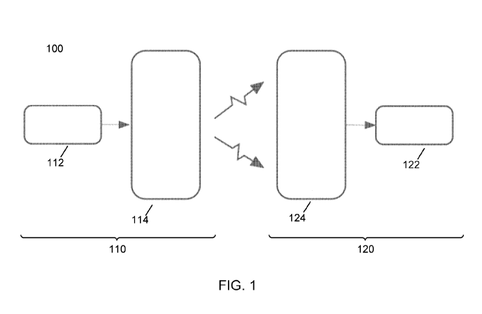
[0082] FIG. 1 shows a wireless power transfer system generally identified
by reference
numeral 100. The wireless power transfer system 100 comprises a transmitter
110 comprising a
power source 112 electrically connected to a transmit element 114, and a
receiver 120
comprising a receive element 124 electrically connected to a load 122. Power
is transferred from
the power source 112 to the transmit element 114. The power is transferred
from the transmit
element 114 to the receive element 124 via resonant or non-resonant electric
or magnetic field
coupling. The power is transferred from the receive element 124 to the load
122.
9
CA 03147123 2022-01-12
WO 2021/007680
PCT/CA2020/050995
[0083] In one example embodiment, the wireless power transfer system may
take the form of
a resonant electric field wireless power transfer system. FIG. 2 shows a
resonant electric field
wireless power transfer system generally identified by reference numeral 200
such as that
described in U.S. Patent No. 9,653,948 to Polu et al. filed on September 7,
2012, the relevant
portions of which are incorporated herein by reference.
[0084] The resonant electric field wireless power transfer system 200
comprises a transmitter
210 comprising a power source 212 electrically connected to a transmit
resonator 214. The
transmit resonator 214 comprises a pair of laterally spaced, elongate transmit
capacitive
electrodes 216, each of which is electrically connected to the power source
212 via a high quality
factor (Q) transmit inductor 218. The system 200 further comprises a receiver
220 comprising a
receive resonator 224 electrically connected to a load 222. The receive
resonator 224 is tuned to
the resonant frequency of the transmit resonator 214. The receive resonator
224 comprises a pair
of laterally spaced, elongate receive capacitive electrodes 226, each of which
is electrically
connected to the load 222 via a high Q receive inductor 228.
[0085] In this embodiment, the inductors 218 and 228 are ferrite core
inductors. One of skill
in the art however will appreciate that other cores are possible.
[0086] In this embodiment, each transmit and receive capacitive electrode
216 and 226
comprises an elongate element formed of electrically conductive material. The
transmit
capacitive electrodes 216 are coplanar. The receive capacitive electrodes 226
are coplanar. In
this embodiment, the transmit capacitive electrodes 216 and the receive
capacitive electrodes 226
are in parallel planes. In this embodiment, the transmit capacitive electrodes
216 and the receive
capacitive electrodes 226 are in the form of generally rectangular, planar
plates.
[0087] While the transmit capacitive electrodes 216 and receive capacitive
electrodes 226
have been described as laterally spaced, elongate electrodes, one of skill in
the art will appreciate
that other configurations are possible including, but not limited to,
concentric, coplanar, circular,
elliptical, disc, etc., electrodes. Other suitable electrode configurations
are described in U.S.
Patent No. 9,979,206 to Nyberg et al. filed on September 4, 2015, the relevant
portions of which
are incorporated herein by reference.
[0088] While the inductors 218 and 228 are shown as being connected in
series to the power
source 212 and the load 222, respectively, in FIG. 2, one of skill in the art
will appreciate that the
CA 03147123 2022-01-12
WO 2021/007680
PCT/CA2020/050995
inductors 218 and 228 may be connected to the power source 212 and the load
222, respectively,
in parallel.
[0089] During operation, power is transferred from the power source 212 to
the transmit
capacitive electrodes 216 via the high Q transmit inductors 218. In
particular, the power signal
from the power source 212 that is transmitted to the transmit capacitive
electrodes 216 via the
high Q transmit inductors 218 excites the transmit resonator 214 causing the
transmit resonator
214 to generate an electric field. When the receiver 220, which is tuned to
the same resonant
frequency as the transmitter 210, is placed within the resonant electric
field, the receive resonator
224 extracts power from the transmit resonator 214 via resonant electric field
coupling. The
extracted power is then transferred from the receive resonator 224 to the load
222. As the power
transfer is highly resonant, the transmit and receive capacitive electrodes
216 and 226,
respectively, need not be as close together or as well aligned as is the case
with the non-resonant
electric field power transfer system. While the transmit resonator 214 may
generate a magnetic
field, little, if any, power is transmitted via magnetic field coupling.
[0090] Turning now to FIG. 3, a block diagram of a wireless power transfer
system in
accordance with an aspect of the disclosure generally identified by reference
numeral 300. The
wireless power transfer system 300 comprises a transmitter 302 and a receiver
304. The
transmitter 302 is configured to transfer power to the receiver 304 via
resonant electric field
coupling as will be described. The receiver 304 is configured to extract power
from the
transmitter 302 via resonant electric field coupling as will be described.
[0091] The transmitter 302 comprises a power source 306, a multi-phase RF
converter 308
and a multi-phase transmit resonator 310. The power source 306 is electrically
connected to the
multi-phase RF converter 308. The power source 306 is configured to generate a
direct current
(DC) power signal. The power source 306 is configured to output the DC power
signal to the
multi-phase RF converter 308. The multi-phase RF converter 308 is electrically
connected to the
power source 306. The multi-phase RF converter 308 is electrically connected
to the multi-
phase transmit resonator 310. The multi-phase RF converter 308 is configured
to convert the DC
power signal into n sinusoidal RF power signals, where n is a positive integer
greater than 2. In
this embodiment, the multi-phase RF converter 308 is a multi-phase RF
inverter. The sinusoidal
RF power signals are shifted out of phase with each other. Each sinusoidal RF
power signal is
shifted 360/n degrees out of phase from successive sinusoidal RF power
signals. The phases are
11
CA 03147123 2022-01-12
WO 2021/007680
PCT/CA2020/050995
distributed such that when the first signal is at 0 degrees, the second signal
is at 360/n degrees,
the third signal is at 2*360/n degrees and the ith signal is at (i-1)*360/n
degrees. The n sinusoidal
RF power signals are output from the multi-phase RF converter 308 to the multi-
phase transmit
resonator 310. The multi-phase transmit resonator 310 is configured to
generate an electric field
and to transfer power via resonant electric field coupling as will be
described. While a magnetic
field may also be generated, little, if any, power is transferred via resonant
or non-resonant
magnetic field coupling. The multi-phase transmit resonator 310 comprises n
electrode/inductor
pairs as will be described.
[0092] The receiver 304 comprises a multi-phase receive resonator 312, a
multi-phase
rectifier 314 and a load 316 The multi-phase receive resonator 312 is
configured to extract
power from the multi-phase transmit resonator 310 via resonant electric field
coupling as will be
described. While a magnetic field may also be present, little, if any, power
is extracted via
resonant or non-resonant magnetic field coupling. The multi-phase receive
resonator 312 is
electrically connected to the rectifier 314. The multi-phase receive resonator
312 comprises
multiple capacitive electrode/inductor pairs as will be described. The multi-
phase receive
resonator 312 comprises n electrode/inductor pairs. The multi-phase receive
resonator 312 is
configured to output multiple sinusoidal RF power signals to the multi-phase
rectifier 314. The
multi-phase receive resonator 312 is configured to output n sinusoidal RF
power signals to the
multi-phase rectifier 314. The sinusoidal RF power signals are shifted out of
phase with each
other. Each sinusoidal RF power signal is shifted 360/n degrees out of phase
from the other
sinusoidal RF power signals. The phases are distributed such that when the
first signal is at 0
degrees, the second signal is at 360/n degrees, the third signal is at 2*360/n
degrees and the ill'
signal is at (i-1)*360/n degrees. The multi-phase rectifier 314 is configured
to convert the
received n sinusoidal RF power signals into a DC power signal. The multi-phase
rectifier 314 is
electrically connected to the load 316. The multi-phase rectifier 314 outputs
the DC power
signal to the load 316. The load 316 is electrically connected to the multi-
phase rectifier 314.
The load 316 receives the DC power signal from the multi-phase rectifier 314.
[0093] Turning now to FIG. 4, a circuit diagram of the wireless power
transfer system 300 is
shown. As previously stated, the wireless power transfer system 300 comprises
the transmitter
302 and the receiver 304. The transmitter 302 comprises the power source 306,
the multi-phase
RF converter 308 and the multi-phase transmit resonator 310.
12
CA 03147123 2022-01-12
WO 2021/007680
PCT/CA2020/050995
[0094] As previously stated, the power source 306 is configured to generate
a DC power
signal. The power source 306 is configured to output the DC power signal to
the multi-phase RF
converter 308.
[0095] The multi-phase RF converter 308 is configured to convert the DC
power signal into
n sinusoidal RF power signals. The multi-phase RF converter 308 comprises n
pairs of switches
402 and a controller (not shown). The pairs of switches 402 are arranged in
parallel. Each pair
of switches 402 outputs a sinusoidal RF power signal. Each sinusoidal RF power
signal is
shifted 360/n degrees out of phase from the other sinusoidal RF power signals.
The phases are
distributed such that when the first signal is at 0 degrees, the second signal
is at 360/n degrees,
the third signal is at 2*360/n degrees and the ith signal is at (i-1)*360/n
degrees. The n sinusoidal
RF power signals are output from the multi-phase RF converter 308 to the multi-
phase transmit
resonator 310.
[0096] In this embodiment, the switches 402 are metal-oxide semiconductor
field-effect
transistors (MOSFETs). In another embodiment, the switches 402 are wide
bandgap devices
(WBDs). In one embodiment, the WBDs are eGaN field-effect transistors (FETs).
The
controller is configured to control switching of the switches 402. In this
embodiment, the
controller is a digital signal processor (DSP). The DSP is configured to send
gate signals to the
switches 402. The gate signals are phase shifted such that the multi-phase RF
converter 308
performs as a multi-phase voltage source with corresponding output voltage.
Specifically, the
gate signal is at (i-1)*360/n phase.
[0097] As previously stated, the multi-phase transmit resonator 310 is
configured to generate
an electric field and to transfer power via resonant electric field coupling
as will be described.
While a magnetic field may also be generated, little, if any, power is
transferred via resonant or
non-resonant magnetic field coupling. The multi-phase transmit resonator 310
comprises n
transmit inductors 404 and n transmit capacitive electrodes 406. Each transmit
inductor 404 is
electrically connected to a transmit capacitive electrode 406. Each transmit
inductor 404 is
electrically connected between a pair of switches 402 of the multi-phase RF
converter 308.
Specifically, the first transmit inductor 404 is electrically connected to the
first transmit
capacitive electrode 406. The first transmit inductor 404 is electrically
connected between the
first pair of switches 402 of the multi-phase RF converter 308. Similarly, the
ith transmit
inductor 404 is electrically connected to the ith transmit capacitive
electrode 406. The ith transmit
13
CA 03147123 2022-01-12
WO 2021/007680
PCT/CA2020/050995
inductor 404 is electrically connected between the ith pair of switches 402 of
the multi-phase RF
converter 308. The ith transmit capacitive electrode 406 and inductor 404 pair
is configured to
resonate at a resonant frequency of the multi-phase transmit resonator 310 at
a phase of (i-
1)*360/n degrees to generate an electric field.
[0098] The receiver 304 comprises the multi-phase receive resonator 312,
the multi-phase
rectifier 314 and the load 316. The multi-phase receive resonator 312 is
configured to extract
power from a generated electric field via resonant electric field coupling.
While a magnetic field
may also be present, little, if any, power is extracted via resonant or non-
resonant magnetic field
coupling. The multi-phase receive resonator 312 comprises n receive capacitive
electrodes 410
and n receive inductors 412. Each receive inductor 412 is electrically
connected to a receive
capacitive electrode 410. Each receive inductor 412 is electrically connected
between a pair of
diodes 414 of the multi-phase rectifier 314. Specifically, the first receive
capacitive electrode
410 is electrically connected to the first receive inductor 412. The first
receive inductor 412 is
electrically connected between the first pair of diodes 414 of the multi-phase
rectifier 314.
Similarly, the ith receive capacitive electrode 410 is electrically connected
to the ith receive
inductor 412. The ith receive inductor 412 is electrically connected between
the ith pair of diodes
414 of the multi-phase rectifier 314. The ith receive capacitive electrode 410
and inductor 412
pair is configured to resonate at a resonant frequency of the multi-phase
transmit resonator 310 at
a phase of (i-1)*350/n degrees to extract power from an electric field via
resonant electric field
coupling. As previously stated, the multi-phase rectifier 314 is configured to
convert the n
sinusoidal RF power signals from the receive multi-phase resonator 312 to a DC
power signal.
The multi-phase rectifier 314 comprises n pairs of diodes 414. The pairs of
diodes 414 are
arranged in parallel. Each pair of diodes 414 receives a sinusoidal RF power
signal. Each
sinusoidal RF power signal is shifted 360/n degrees out of phase from the
other sinusoidal RF
power signals. The phases are distributed such that when the first signal is
at 0 degrees, the
second signal is at 360/n degrees, the third signal is at 2*360/n degrees and
the ith signal is at (i-
1)*360/n degrees. The n sinusoidal RF power signals are rectified into a DC
power signal that is
output to the load 316.
[0099] As shown in FIG. 4, the capacitance of the 1th transmit capacitive
electrode 406 to
ground is represented by the capacitance CUTE. The capacitance of the receive
capacitive
electrode 410 to ground is represented as CGR). The capacitance of the ith
transmit capacitive
14
CA 03147123 2022-01-12
WO 2021/007680 PCT/CA2020/050995
electrode 406 and the adjacent transmit capacitive electrode 406 is
represented as Cmyo-pp. The
capacitance of the ith transmit capacitive electrode 406 and the jth transmit
capacitive electrode
406 is represented as CmTij (not shown). The capacitance of the ith receive
capacitive electrode
410 and the adjacent receive capacitive electrode 410 is represented as
CiviRo+/). The capacitance
of the ith receive capacitive electrode 410 and thet receive capacitive
electrode 410 is
represented as Civimi (not shown). The capacitance of the ith transmit
capacitance electrode 406
and the adjacent ith receive capacitive electrode 410 is represented as
CAITR,i. Similarly, the
capacitance of the ith receive capacitive electrode 410 and the adjacent ith
transmit capacitance
electrode 406 is represented as CA4TRii. The capacitance of the ith transmit
capacitance electrode
406 and the jth receive capacitive electrode 410 is represented as Cmmu (not
shown) Similarly,
the capacitance of the the jth receive capacitive electrode 410 and the ith
transmit capacitance
electrode 406 is represented as Gump (not shown). The inductance of the
transmit inductor 404
is represented as LTI. The inductance of the receive inductor 412 is
represented as LRI. The term
i is an integer between, and including, 1 and n, where 1+1 is at most equal to
n. When i is equal
to n, then i+1 is understood to be 1, as the labelling is periodic. The term j
is an integer between,
and including, 1 and n.
101001 As described above, the multi-phase receive resonator 312 has n
pairs of receive
capacitive electrodes 410 and inductors 412. Each pair of receive capacitive
electrodes 410 and
inductors 412 carries one of the n sinusoidal RE power signals to the multi-
phase rectifier 314
and then to the load 316. The wireless power transfer system 300 is balanced
when all n pairs of
receive capacitive electrodes 410 and inductors 412 carry currents that are of
the same amplitude
and frequency, but differ in phase by 360/n degrees between successive
branches, such that the
sum of the currents on all pairs of receive capacitive electrodes 410 and
inductors 412 is zero. If
the sum of the currents on all pairs of receive capacitive electrodes 410 and
inductors 412 is non-
zero, an additional return path to ground must exist. As there are no
additional physical
connections between the multi-phase transmit and receive resonators 310 and
312, respectively,
beyond the capacitances Cmmjõ this non-zero sum current manifests as a current
returning
through the environment. The performance of the system 400 is dependent on the
impedance of
the return path In this embodiment, performance includes one or more of
efficiency, power
delivery, electromagnetic interference (EMI) and heating. The impedance of the
return path
depends on the geometry and electrical properties of any objects in the
surrounding environment
CA 03147123 2022-01-12
WO 2021/007680
PCT/CA2020/050995
of the system. Furthermore, an unbalanced system may exhibit common-mode or
ground return
current. Therefore, an unbalanced system will be less robust as an unbalanced
system will be
more affected by the impedance of any objects in the surrounding environment
of the system
than a balanced system.
[0101] The wireless power transfer system 300 has an impedance presented at
an input and
an output thereof. When transferring power from the power source 306 to the
load 316, the
impedance presented at the input and output of the wireless power transfer
system 300 must be
balanced such that all sinusoidal RF power signals output from the multi-phase
RF converter 308
encounter substantially the same impedance while entering the multi-phase
transmit resonator
310 and while exiting the multi-phase receive resonator 312. If the wireless
power transfer
system 300 is unbalanced, energy will be lost during the wireless power
transfer as energy output
from the power source 306 is emitted as heat or sunk into ground. A balanced
wireless power
transfer system 300 eliminates common mode noise within the wireless power
transfer system
300. Provided with a balanced multi-phase RF converter 308 and a balanced load
316 of the
wireless power transfer system 400, the wireless power transfer system 400
will be balanced
when certain requirements are met. Specifically, the following conditions must
be met in order
for the wireless power transfer system 400 to be balanced:
LT1 = LT2 = === = LTn
CGT1 = CGT2 = === = CGTn
CMT12 = CMT23 = = CMT(n-1)n = CMTn1
CMT1(1-Fi) = CMT2(2-Fi) = === = CMTni
41 - 42 ¨ === ¨ 4n
CGR1 = CGR2 = === = CGRn
CMR12 = CMR23 = = CMR(n-1)n = CMRn1
CMR1(1+0 = CMR2(2+0 = === = CMRni
CMTR11 = CMTR22 = === = CMTRnn
CMTR1(1+0 = CMTR2(2+0 = = CMTRni
CMTR(1+i)1 = CMTR(2+i)2 = === = CMTRin
[0102] These conditions are met if the capacitive electrodes 404 and 416
have identical
dimensions and configurations, and the inductors 404 and 412 have identical
dimensions and
configurations.
16
CA 03147123 2022-01-12
WO 2021/007680 PCT/CA2020/050995
[0103] During operation, the power source 306 outputs a DC power signal to
the multi-phase
RF converter 308. The multi-phase RF converter 308 converts the DC power
signal into n
sinusoidal RF power signals. The controller sends gate signals to the switches
402 such that
each pair of switches 402 of the multi-phase RF converter 308 outputs one of
the sinusoidal RF
power signals to an transmit inductor 404 and capacitive electrode 406 pair of
the multi-phase
transmit resonator 310. Each transmit inductor 404 and capacitive electrode
406 pair resonate at
a resonant frequency of the multi-phase transmit resonator 301 to generate an
electric field.
Specifically, the 1t11 pair of transmit inductor 404 and capacitive electrode
406 resonate at the
resonant frequency at a phase of (i-1)*360/n degrees to generate an electric
field. When the
multi-phase receive resonator 312 is within the electric field generated by
the multi-phase
transmit resonator 310, the electric field excites the multi-phase receive
resonator 312 through
resonant electric field coupling. Power is then wirelessly extracted by the
multi-phase receive
resonator 314 from the multi-phase transmit resonator 310. The multi-phase
receive resonator
312 outputs the received sinusoidal RF power signals to the multi-phase
rectifier 314. The multi-
phase rectifier 314 rectifies the sinusoidal RF power signals to a DC power
signal. The DC
power signal is then applied to the load 316.
[0104] The higher number of phases in the wireless power transfer system
300, compared to
the wireless power transfer system 200, increases the maximum output power of
the multi-phase
RF converter 308 (for a given switch 402 and voltage input into the multi-
phase RF converter
308), as each phase requires a dedicated pair of switches 402 to handle a
limited amount of
current and voltage. The maximum output power of the multi-phase RF converter
308 scales
linearly with the number of phases. For a transmit multi-phase resonator 310
with a fixed area
for the transmit capacitive electrodes 406, increasing the number of transmit
capacitive
electrodes 406 reduces the area of each transmit capacitive electrode 406.
Since the input
capacitance of each transmit capacitive electrode 406 is dependent on the area
of the respective
transmit capacitive electrode 406, increasing the number of transmit
capacitive electrodes 406
decreases the input capacitance of each transmit capacitive electrode 406. The
input capacitance
is defined as the capacitance seen looking into the respective transmit
capacitive electrode 406 or
the capacitance that must be compensated by the transmit inductor 404 to
achieve resonance at
the resonant frequency; therefore, additional phases require additional
inductance per transmit
capacitive electrode 406. For each additional phase, the multi-phase RF
converter 308 requires
17
CA 03147123 2022-01-12
WO 2021/007680 PCT/CA2020/050995
at least one additional metal-oxide semiconductor field-effect transistor
(MOSFET) or wide
bandgap device (WBD) switch 402, each multi-phase transmit resonator 310
requires at least one
additional transmit inductor 404, and the multi-phase rectifier 314 requires
at least one additional
diode 414.
[0105] The wireless power transfer system 300 may be used for, but not
limited to, transfer
power in systems with lateral or rotational motion. The wireless power
transfer system 300 may
also be used to transfer power for a variety of rotational systems, such as
through a rotating joint.
A rotating joint is defined as a device comprising two or more joined parts,
wherein at least one
part rotates. The wireless power transfer system 300 maintains efficient power
transfer
throughout 360 degrees of rotation.
[0106] While a wireless power transfer system 300 has generally been
described, one of skill
in the art will appreciate that particular embodiments are possible. FIG. 5A
shows a circuit
diagram of a wireless power transfer system generally identified by reference
numeral 500. The
wireless power transfer system 500 is an embodiment of the wireless power
system 300 in which
the integer n is equal to 3. The wireless power transfer system 300 comprises
a transmitter 502
and a receiver 504. The transmitter 502 is configured to transfer power to the
receiver 504 via
resonant electric field coupling as previously described. The receiver 504 is
configured to
extract power from the transmitter 502 via resonant electric field coupling as
previously
described.
[0107] The transmitter 502 comprises a power source 506, a multi-phase RF
converter 508
and a multi-phase transmit resonator 512. The power source 506 is electrically
connected to the
multi-phase RF converter 508. The power source 506 is configured to generate a
DC power
signal. The power source 506 is configured to output the DC power signal to
the multi-phase RF
converter 508. The multi-phase RF converter 508 is electrically connected to
the power source
506. The multi-phase RF converter 508 is electrically connected to the multi-
phase transmit
resonator 512. The multi-phase RF converter 508 is configured to convert the
DC power signal
into three (3) sinusoidal RF power signals. The sinusoidal RF power signals
are shifted out of
phase with each other. Each sinusoidal RF power signal is shifted 360/3
degrees out of phase
from successive sinusoidal RF power signals. The phases are distributed such
that when the first
signal is at 0 degrees, the second signal is at 120 degrees and the third
signal is at 240 degrees.
18
CA 03147123 2022-01-12
WO 2021/007680 PCT/CA2020/050995
The three sinusoidal RF power signals are output from the multi-phase RF
converter 508 to the
multi-phase transmit resonator 512.
[0108] In this embodiment, the multi-phase RF converter 508 is a three-
phase RF inverter.
The multi-phase RF converter 508 comprises three pairs of switches 510 and a
controller (not
shown). The pairs of switches 510 are arranged in parallel. Each pair of
switches 510 outputs a
sinusoidal RF power signal. Each sinusoidal RF power signal is shifted 120
degrees out of
phase. The three sinusoidal RF power signals are output from the multi-phase
RF converter 508
to the multi-phase transmit resonator 512.
[0109] In this embodiment, the switches 510 are MOSFETs. In another
embodiment, the
switches 510 are WBDs. In one embodiment, the WBDs are eGaN field-effect
transistors
(FETs). The controller is configured to send gate signals to the switches 510
to control
switching of the switches 510. In this embodiment, the controller is a DSP.
The DSP is
configured to send gate signals to the switches 402. The gate signals are
phase shifted such that
the multi-phase RF converter 308 performs as a multi-phase voltage source with
corresponding
output voltage. For example, in a three-phase system, the gate signals would
be in 120 degrees
phase shifts (360 degrees/3) such that the output voltage of the three-phase
converter performs as
a 3-phase voltage source.
[0110] In this embodiment, the multi-phase transmit resonator 512 is a
three-phase transmit
resonator. The multi-phase transmit resonator 512 is configured to generate an
electric field and
to transfer power via resonant electric field coupling. While a magnetic field
may also be
generated, little, if any, power is transferred via resonant or non-resonant
magnetic field
coupling. The multi-phase transmit resonator 512 comprises three transmit
inductors 514 and
three transmit capacitive electrodes 516. Each transmit inductor 514 is
electrically connected to
a transmit capacitive electrode 516. Each transmit inductor 514 is
electrically connected
between a pair of switches 510 of the multi-phase RF converter 508. In this
embodiment, each
transmit inductor 514 is directly electrically connected to a respective
transmit capacitive
electrode 516. The first transmit inductor 514 is electrically connected
between the first pair of
switches 510 of the multi-phase RF converter 508. The first electrically
connected pair of
transmit inductor 514 and capacitive electrode 516 is configured to resonate
at a resonant
frequency of the multi-phase transmit resonator 512 at a phase of 0 degrees to
generate an
electric field. The second electrically connected pair of transmit inductor
514 and capacitive
19
CA 03147123 2022-01-12
WO 2021/007680
PCT/CA2020/050995
electrode 516 is configured to resonate at a resonant frequency of the multi-
phase transmit
resonator 512 at a phase of 120 degrees to generate an electric field. The
third electrically
connected pair of transmit inductor 514 and capacitive electrode 516 is
configured to resonate at
a resonant frequency of the multi-phase transmit resonator 512 at a phase of
240 degrees to
generate an electric field.
[0111] The receiver 504 comprises a multi-phase receive resonator 520, a
multi-phase
rectifier 526 and a load 530. The multi-phase receive resonator 520 is
configured to extract
power from the multi-phase transmit resonator 512 via resonant electric field
coupling. While a
magnetic field may also be present, little, if any, power is extracted via
resonant or non-resonant
magnetic field coupling. The multi-phase receive resonator 520 is electrically
connected to the
multi-phase rectifier 526.
[0112] In this embodiment, the multi-phase receive resonator 520 is a three-
phase receive
resonator. The multi-phase receive resonator 520 is configured to output three
sinusoidal RF
power signals to the multi-phase rectifier 526. The sinusoidal RF power
signals are shifted out
of phase with each other. Each sinusoidal RF power signal is shifted 120
degrees out of phase.
The phases are distributed such that when the first signal is at 0 degrees,
the second signal is at
120 degrees and the third signal is at 240 degrees. The multi-phase receive
resonator 520
comprises three receive capacitive electrodes 522 and three receive inductors
524. Each receive
inductor 524 is electrically connected to a receive capacitive electrode 522.
In this embodiment,
each receive inductor 524 is directly electrically connected to a respective
receive capacitive
electrode 522. Each receive inductor 524 is electrically connected between a
pair of diodes 528
of the multi-phase rectifier 526. The first receive capacitive electrode 522
and inductor 524 pair
is configured to resonate at a resonant frequency of the multi-phase transmit
resonator 512 at a
phase of 0 degrees to extract power from an electric field via resonant
electric field coupling.
The second receive capacitive electrode 522 and inductor 524 pair is
configured to resonate at a
resonant frequency of the multi-phase transmit resonator 512 at a phase of 120
degrees to extract
power from an electric field via resonant electric field coupling. The third
receive capacitive
electrode 522 and inductor 524 pair is configured to resonate at a resonant
frequency of the
multi-phase transmit resonator 512 at a phase of 240 degrees to extract power
from an electric
field via resonant electric field coupling.
CA 03147123 2022-01-12
WO 2021/007680 PCT/CA2020/050995
[0113] In this embodiment, the multi-phase rectifier 526 is a three-phase
rectifier. The
multi-phase rectifier 526 is configured to convert the received three
sinusoidal RF power signals
into a DC power signal. The multi-phase rectifier 526 is electrically
connected to the load 530.
The multi-phase rectifier 526 outputs the DC power signal to the load 530. The
multi-phase
rectifier 526 comprises three pairs of diodes 528. The pairs of diodes 528 are
arranged in
parallel. Each pair of diodes 528 receives a sinusoidal RF power signal. Each
sinusoidal RF
power signal is shifted 120 degrees out of phase. The three sinusoidal RF
power signals are
rectified into a DC power signal that is output to the load 530.
[0114] The load 530 is electrically connected to the multi-phase rectifier
526. The load 530
receives the DC power signal from the multi-phase rectifier 526.
[0115] As shown in FIG. 5, the capacitance of the ith transmit capacitive
electrode 516 to
ground is represented by the capacitance CGTI. The capacitance of the ith
receive capacitive
electrode 522 to ground is represented as CGR). The capacitance of the 1th
transmit capacitive
electrode 516 and the adjacent transmit capacitive electrode 516 is
represented as Cmyo+/). The
capacitance of the ith transmit capacitive electrode 516 and the jth transmit
capacitive electrode
516 is represented as CmTru (not shown). The capacitance of the 1th receive
capacitive electrode
522 and the adjacent receive capacitive electrode 522 is represented as
CA4R0+/). The capacitance
of the ith receive capacitive electrode 522 and the jth receive capacitive
electrode 522 is
represented as GIRIJ (not shown). The capacitance of the ith transmit
capacitance electrode 516
and the adjacent ith receive capacitive electrode 522 is represented as
CAITRii. Similarly, the
capacitance of the ith receive capacitive electrode 522 and the adjacent ith
transmit capacitance
electrode 516 is represented as CmTR,i. The capacitance of the ith transmit
capacitance electrode
516 and the adjacent jth receive capacitive electrode 522 is represented as
Cmmu (not shown).
Similarly, the capacitance of thet receive capacitive electrode 522 and the
ith transmit
capacitance electrode 516 is represented as CivrrRii (not shown). The
inductance of the transmit
inductor 510 is represented as LT,. The inductance of the receive inductor 524
is represented as
Lib. The term i is an integer between, and including, 1 and 3, where i+1 is at
most equal to 3.
The term j is an integer between, and including, 1 and 3.
[0116] As previously discussed with reference to the wireless power
transfer system 400
with a balanced multi-phase RF converter 508 and a balanced load 530 of the
wireless power
transfer system 500, the wireless power transfer system 500 will be balanced
when certain
21
CA 03147123 2022-01-12
WO 2021/007680
PCT/CA2020/050995
requirements are met. Specifically, the following conditions must be met in
order for the
wireless power transfer system 500 to be balanced:
LT1 ¨ LT2 ¨ LT3
CGT1 = CGT2 = CGT3
CMT12 = CMT23 = CMT31
LR1 = LR2 = LR3
CGR1 = CGR2 = CGR3
CMR12 CMR23 = CMR31
CMTR11 = CMTR22 = CMTR33
CMTR12 = CMTR21 = CMTR23 = CMTR32 = CMTR31 = CMTR13
[0117] These conditions are met if the capacitive electrodes 516 and 522
have identical
dimensions and configurations, and the inductors 510 and 524 have identical
dimensions and
configurations.
[0118] A simulation was performed to determine the performance of the multi-
phase rectifier
526 compared to a conventional single-phase rectifier. FIG. 5B is a graph of
the load voltage
output by the multi-phase rectifier 526 of the wireless power transfer system
500 compared to
load voltage output by a single-phase rectifier. As shown in FIG. 5B, the load
voltage output by
the multi-phase rectifier 526 exhibits less ripple than the load voltage
output by the single-phase
rectifier.
[0119] As shown in FIG. 6, in this embodiment of the wireless power
transfer system 500,
the transmit capacitive electrodes 516 of the multi-phase transmit resonator
512 comprise three
generally elongate planar plates. The plates are coplanar. The plates are
generally rectangular.
The plates are laterally spaced. The plates comprise a first plate 602, a
second plate 604 and a
third plate 606. The first plate 602 is spaced apart from the second plate 604
and generally
parallel with the second plate 604. The second plate 604 is spaced apart from
the first plate 602
and the third plate 606, and generally parallel with the first plate 602 and
the third plate 606.
The third plate 606 is spaced apparat from the second plate 604 and generally
parallel with the
second plate 604. The first and third plates 602 and 606, respectively, are
identical in shape and
size. The first, second and third plates 602, 604 and 606, respectively, have
the same length.
22
CA 03147123 2022-01-12
WO 2021/007680
PCT/CA2020/050995
[0120] In this embodiment, the first plate 602 and the third plate 606 are
electrically
connected via a lumped capacitor 608. The lumped capacitor 608 compensates for
weak
capacitance between the first plate 602 and the third plate 606.
[0121] As previously stated, the mutual capacitance between adjacent plates
is represented as
capacitance Cmt and the capacitance to ground of each plate is represented as
capacitance Cg.
The second plate 604 has a greater width than the widths of the first and
third plates 602 and 606,
respectively. The second plate 604 has the greater width in order for the
second plate 604 to
maintain the same capacitance to ground Cg as the first and third plates 602
and 606,
respectively. While the transmit capacitance electrodes 516 have been
described, one of skill in
the art will appreciate that the receive capacitive electrodes 522 may be
similarly configured.
[0122] While the transmit capacitive electrodes 516 have been described as
having a
particular configuration, one of skill in the art will appreciate that other
configurations are
possible. FIGs. 7 and 8 show another embodiment of the transmit capacitive
electrodes 516
generally identified as reference numeral 700. In this embodiment, the
transmit capacitive
electrodes 700 comprise n (three) rows of electrodes 702, 704 and 706, one for
each phase of the
multi-phase transmit resonator 512. Each row of electrodes 702, 704 and 706
comprises 3 *m+1
(four) plates, where m is a positive integer. In this embodiment m is 1. The
plates are generally
elongate planar plates. In this embodiment, the plates are coplanar. The
plates are laterally
spaced. The plates in each row of electrodes 702, 704 and 706 comprise a first
plate 710, a
second plate 712, a third plate 714 and a fourth plate 716. The first plate
710 and fourth plate
716 are identical. The first plate 710 and the fourth plate 716 are generally
rectangular. The
second plate 712 and third plate 714 are identical. The second plate 712 and
the third plate 714
are generally rectangular. The second plate 712 and the third plate 714 have
twice the length of
the first and fourth plates 710 and 716.
[0123] The first plate 710 is spaced apart from the second plate 712 and
generally parallel
with the second plate 712. The second plate 712 is spaced apart from the first
plate 710 and the
third plate 714, and generally parallel with the first plate 710 and the third
plate 714. The third
plate 714 is spaced apart from the second plate 712 and the fourth plate 716,
and generally
parallel with the second plate 712 and the fourth plate 716. The fourth plate
716 is spaced apart
from the third plate 714 and generally parallel with the third plate 714. The
first, second, third
23
CA 03147123 2022-01-12
WO 2021/007680
PCT/CA2020/050995
and fourth plates 710, 712, 714 and 716, respectively, have the same height.
The second plate
712 and the third plate 714 have double the length of the first plate 710 and
the fourth plate 716.
[0124] As shown in FIGs. 7 and 8, the first, second and third plates 710,
712 and 714,
respectively, in the first row of electrodes 702 are electrically connected
via out-of-plane traces
to the second, third and fourth plates 712, 714 and 716, respectively, of the
third row of
electrodes 702. The second, third and fourth plates 712, 714 and 716,
respectively, of the first
row of electrodes 702 are electrically connected via in-plane traces to the
first, second and third
plates 710, 712 and 714, respectively, of the second row of electrodes 704.
The second, third
and fourth plates 712, 714 and 716, respectively, of the second row of
electrodes 704 are
electrically connected via in-plane traces to the first, second and third
plates 710, 712 and 714,
respectively, of the third row of electrodes 706.
[0125] The configuration of transmit capacitive electrodes 700 shown in
FIGs. 7 and 8
ensures that the multi-phase transmit resonator 512 is approximately balanced.
[0126] While transmit capacitance electrodes 700 have been described, one
of skill in the art
will appreciate that the receive capacitive electrodes 522 may be similarly
configured.
[0127] While the embodiments of the transmit capacitive electrodes 516
described and
shown in FIGs. 6 to 8 have been described separately, one of skill in the art
will appreciate that
they may be combined. Turning now to FIG. 9, a plan view of another embodiment
of the
receive capacitive electrodes 522 is shown generally identified by reference
numeral 1100. The
receive capacitive electrodes 1100 comprise the first plate 602, second plate
604 and third plate
606. In this embodiment, the transmit capacitive electrodes 516 are generally
identified by
reference numeral 1110. The transmit capacitive electrodes 1110 comprise the
rows of
electrodes 702, 704 and 706 having the first plate 710, second plate 712,
third plate 714 and
fourth plate 716.
[0128] A simulation was performed to determine the performance of the
wireless power
transfer system 300 with the receive capacitive electrodes 1100 comprising the
first plate 602,
second plate 604 and third plate 606, and the transmit capacitive electrodes
1110 comprising the
rows of electrodes 702, 704 and 706 having the first plate 710, second plate
712, third plate 714
and fourth plate 716. In the simulation, the receive capacitive electrodes
1100 were moved along
the horizontal span of the transmit capacitive electrodes 1110 from a starting
position of 0 mm to
a final position of 300 mm. FIG. 10 is a graph of the RF efficiency at a
resonant frequency of
24
CA 03147123 2022-01-12
WO 2021/007680
PCT/CA2020/050995
13.56 MHz as a function of the movement of the receive capacitive electrodes
1100 along the
horizontal span of the transmit capacitive electrodes 1110. The RF efficiency
is defined as the
efficiency of the wireless power transfer between the multi-phase transmit and
receive resonators
512 and 520, respectively. As shown in FIG. 10, the RF efficiency is
maintained at a level above
90%.
[0129] While exemplary transmit and receive capacitive electrodes have been
described as
being rectangular or square, one of skill in the art will appreciate that
other configurations are
possible. In another embodiment, the transmit capacitive electrodes 406
comprise n identical
planar transmit segments. The transmit segments are equally spaced around a
central point
within a plane. The transmit segments are symmetric upon 360/n degree
rotations about an axis
perpendicular to the plane extending from the central point. The transmit
segments are separated
from each other. In this embodiment, the n transmit capacitive electrodes form
a transmit
capacitor. During use, the transmit capacitor resonates the reactance of the n
transmit inductors
404 at the operating frequency of the RF converter 308. Each transmit inductor
404 resonates
with the input capacitance of the corresponding transmit segment.
[0130] The receive capacitive electrodes 410 comprise n identical planar
receive segments.
The receive segments are equally spaced around a central point within a plane.
The receive
segments are symmetric upon 360/n degree rotations about an axis perpendicular
to the plane
extending from the central point. The receive segments are separated from each
other. In this
embodiment, the n receive capacitive electrodes form a receive capacitor.
[0131] During use, the multi-phase transmit resonator 310 is aligned with
the multi-phase
receive resonator 312 such that the major surfaces of the transmit segments
and receive segments
face each other, with the central point of each resonator 310 and 312 located
directly transverse
from each other. The receive segments may rotate at an angle 0 about an axis
perpendicular to
the plane of the receive segments passing through the central point of the
receive capacitor.
When the transmit segments are rotationally aligned with the receive segments,
each receive
segment is closely coupled with a corresponding transmit segment. Therefore,
each receive
segment is driven at the phase of the corresponding transmit segment. At this
position 0 is set to
0. Due to the rotational symmetry of the transmit and receive segments,
positions where
0=p*360/n (where p is any integer) will be indistinguishable from the position
where 0=0 and
therefore each other.
CA 03147123 2022-01-12
WO 2021/007680
PCT/CA2020/050995
[0132] While the transmit capacitive electrodes 516 have been described as
having a
particular configuration, one of skill in the art will appreciate that other
configurations are
possible. FIG. 11 shows another embodiment of the transmit capacitive
electrodes 516 generally
identified by reference numeral 1400. In this embodiment, the transmit
capacitive electrodes
1400 comprise three segments 1402. In this embodiment, the segments 1402 are
plates. The
segments 1402 are coplanar. The segments 1402 are identically sized. The
segments 1402 are
spaced apart such that they generally form a circle about their
circumferences. Each segment
1402 spans approximately 120 degrees of the circle. The segments 1402 are
equally spaced
around a central point within a plane. The segments 1402 have an axis of a
three-fold rotational
symmetry normal to the major face of the segments 1402 about the centre of
curvature of the
segments 1402. While the transmit capacitance electrodes 1400 have been
described, one of skill
in the art will appreciate that the receive capacitive electrodes 522 may be
similarly configured.
[0133] While the wireless power transfer system 500 has been described, one
of skill in the
art will appreciate that other configurations are possible. FIG. 12 shows a
partial wireless power
transfer system generally identified by reference numeral 1500. The wireless
power transfer
1500 comprises a transmitter and a receiver. The transmitter is identical to
the previously
described transmitter 502 unless otherwise stated. The receiver is identical
to the previously
described receiver 504 unless otherwise stated.
[0134] In this embodiment, the multi-phase transmit resonator 512 comprises
transmit
capacitive electrodes 1502. The transmit capacitive electrodes 1502 comprise
three transmit
segments 1504. In this embodiment, the transmit segments 1504 are plates. The
transmit
segments 1504 are coplanar. The transmit segments 1504 are identically sized.
The transmit
segments 1504 are spaced apart such that they generally form a circle about
their circumferences.
Each transmit segment 1504 spans approximately 120 degrees of the circle. The
transmit
segments 1504 are equally spaced around a central point within a plane. The
transmit segments
1504 have an axis of a three-fold rotational symmetry normal to the major face
of the transmit
segments 1504 about the centre of curvature of the transmit segments 1504.
Each transmit
segment 1504 is paired with an inductor 514 ensuring that the multi-phase
transmit resonator 512
is configured to resonate at the resonant frequency of the multi-phase
transmit resonator 512.
The inductors 514 of the multi-phase transmit resonator 512 are identical.
Given the
26
CA 03147123 2022-01-12
WO 2021/007680 PCT/CA2020/050995
symmetrical positioning of the transmit segments 1504, the multi-phase
transmit resonator 512 is
balanced.
[0135] In this embodiment, each transmit segment 1504 has an outer radius
of 150 mm, an
inner radius of 30 mm and a thickness of 0.1 mm. Each transmit segment 1504 is
separated from
the adjacent transmit segment 1504 by a 10 mm gap.
[0136] In this embodiment, the multi-phase receive resonator 520 comprises
receive
capacitive electrodes 1510. The receive capacitive electrodes 1510 comprise
three receive
segments 1512. In this embodiment, the receive segments 1512 are plates. The
receive
segments 1512 are coplanar. The receive segments 1512 are identically sized.
The receive
segments 1512 are spaced apart such that they generally form a circle about
their circumferences.
Each receive segment 1512 spans approximately 120 degrees of the circle. The
receive segments
1512 are equally spaced around a central point within a plane. The receive
segments 1512 have
an axis of a three-fold rotational symmetry normal to the major face of the
receive segments
1512 about the centre of curvature of the receive segments 1512. Each receive
segment 1512 is
paired with an inductor 524 ensuring the multi-phase receive resonator 520 is
configured to
resonate at the resonant frequency. Given the symmetrical positioning of the
receive segments
512, the multi-phase receive resonator 520 is balanced. As both the multi-
phase transmit and
receive resonators 512 and 520 are balanced, the wireless power transfer
system 1500 is
balanced.
[0137] In this embodiment, each receive segment 1512 has an outer radius of
150 mm, an
inner radius of 30 mm and a thickness of 0.1 mm. Each receive segment 1512 is
separated from
the adjacent receive segment 1512 by a 10 mm gap.
[0138] In this embodiment both the transmit and receive inductors 514 and
524, respectively,
have an inductance of 9.98 H and a quality factor (Q) of 225. The transmit
capacitive
electrodes 1502 and receive capacitive electrodes 1510 have identical geometry
and are located
50 mm away each other. The transmit capacitive electrodes 1502 and receive
capacitive
electrodes 1510 have a common axis of three-fold rotational symmetry.
[0139] The wireless power transfer system 1500 may be implemented in
rotating structures.
Rotating structures may take the form of a slip ring, helicopter, swivelling
chair, etc. When the
wireless power transfer system 1500 is implemented in rotating structures, the
transmit
capacitive electrodes 1502 and the receive capacitive electrodes 1510 rotate
through 360 degrees
27
CA 03147123 2022-01-12
WO 2021/007680 PCT/CA2020/050995
of rotation. Due to the three-fold rotational symmetry of the electrodes 1502
and 1510,
establishing that the leakage current of the wireless power transfer system
1500 is negligible for
all angular positions 0 from 0 to 120 degrees demonstrates that the wireless
power transfer
system 1500 is balanced.
[0140] Simulations were performed to determine the performance of the
wireless power
transfer system 1500 and establish that the leakage current of the wireless
power transfer system
1500 is negligible for all angular positions 0 from 0 to 120 degrees. FIG. 13
is a plot of the ratio
of the sum of the current on each segment 1504 and 1512 to the sum of the
magnitude of the
current on each segment 1504 and 1512 as a percentage for a rotation from 0 to
120 degrees for
both transmit and receive capacitive electrodes 1502 and 1510, respectively.
The sum of the
current on each segment 1504 and 1512 is defined as the common mode current.
The ratio in
FIG. 13 is given by:
il + i2 + i3
i2i2* i3i;
where ii,i2 and i3 are the currents on the first, second, and third segments
1504 and 1512 of the
respective transmit and receive capacitive electrodes 1502 and 1510,
respectively.
[0141] Throughout 120 rotation, the sum of the currents on each segment
1504 and 1512 is
less than 0.05% of the root mean square (RMS) of the currents. A sum of the
currents of less
than 0.05% of the RMS of the currents corresponds to a common mode rejection
radio (CMRR)
of 66 dB. Therefore, leakage currents are negligible, and the wireless power
transfer system
1500 remains balanced under rotation.
[0142] FIG. 14 is a graph of the phase of the current signal on each
receive segment 1512 as
a function of angular position 0 (rotation angle). The phase of the current on
each receive
segment 1512 decreases almost linearly from 180 to -180 degrees (or
equivalently 0 to 360
degrees) over a rotation of 360 degrees. The phase curves sinusoidally away
from linearity with
a periodicity of 120 degrees, reflecting the structure of the receive
capacitive electrodes 510. A
numerical model of each line in the graph of FIG. 14 is provided in Equations
1A, 1B and 1C
below:
Phase 1= ¨0 + offset + A * sin(3 * 0 +)+ 0
(Equation 1A)
Phase 2 = ¨0 + offset +A * sin(3 * 0 + tp) + 120
(Equation 1B)
Phase 3 = ¨0 + offset + A * sin(3 * 0 + tp) + 240
(Equation 1C)
28
CA 03147123 2022-01-12
WO 2021/007680 PCT/CA2020/050995
where A is an amplitude of sinusoidal oscillation and u is a phase constant.
[0143] The modelling parameters for Equations 1A, 1B and 1C are provided in
Table 1
below.
Parameter Value Standard Error
offset 37.25 0.17
A 10 09 0.25
9.01 1.35
Table 1
[0144] As described by Equations 1A, 1B and 1C, the phase difference
between two adjacent
transmit or receive capacitive electrodes 1502 or 1510 is 120 degrees for any
rotational angle,
allowing continuous wireless power transfer while the multi-phase receive
resonator 512 rotates
relative to the multi-phase transmit resonator 520. The constant phase
separation of 120 ensures
the wireless power transfer system 1500 is balanced. Therefore, as established
through
simulation, the leakage current of the wireless power transfer system 1500 is
negligible for all
angular positions 0 from 0 to 120 degrees.
[0145] Further simulations were performed to establish the RF efficiency
and input
impedance of the wireless power transfer system 1500 when implemented in
rotating structures.
Through these simulations, it was found that the RF efficiency stayed nearly
constant during
rotation of the transmit capacitive electrodes 1502 and receive capacitive
electrodes 1504 of the
wireless power transfer system 1500 and thus, provided predictable
performance. However, the
input impedance varies significantly during rotation of the transmit
capacitive electrodes 1502
and receive capacitive electrodes 1504 of the wireless power transfer system
1500. Generally,
during rotation of the transmit capacitive electrodes 1502 and receive
capacitive electrodes 1504
of the wireless power transfer system 1500, the properties, including RF
efficiency and input
impedance, of the wireless power transfer system 1500 oscillate at n times the
frequency of
rotation about the mean value of the properties. The properties can be
numerically approximated
by the form provided in Equation 2 below:
g(0) = + Amp * sin(n * 0 + 4-) (Equation 2)
29
CA 03147123 2022-01-12
WO 2021/007680 PCT/CA2020/050995
where g(8) is the particular property as a function of rotation angle 8 in
degrees, g is the mean
value of the property, Amp is the amplitude of oscillation defined as the
difference between
either extrema and the mean value g, n is the number of phases, and is a phase
constant.
[0146] The RF efficiency, real part of the impedance, and imaginary part of
the impedance of
the wireless power transfer system 1500 are numerically described by using the
modelling
parameters in Table 2 below in Equation 2. The real and imaginary parts of the
impedance of the
wireless power transfer system 1500 are the components of the input impedance
of the wireless
power transfer system 1500.
g AMP
RF Efficiency 94.62 +/- 0.05 % 0.96 +/- 0.4 % 74 +/- 4 degrees
Real Part of the 203 +/- 2 Q 90 +/- 1 Q 102 +/- 2 degrees
Impedance
Imaginary Part of the 30 +/- 0.8 Q 30 +/- 0.7 Q 131 +1-2 degrees
Impedance
Table 2
[0147] FIG. 15 is a graph of the RF efficiency of the wireless power
transfer system 1500 at
a resonant frequency of 13.56 MHz as a function of angular rotation over 120
degrees. The RF
efficiency is defined as the efficiency of the wireless power transfer between
the multi-phase
transmit and receive resonators 512 and 520, respectively. The RF efficiency
shown in FIG. 15
is characterized by Equation 2 with the modeling parameters of Table 2. The
offset parameter is
large in comparison to the amplitude; therefore, the wireless power transfer
system 1500
maintains an RF efficiency over 94.5 % over 120 degrees of rotation.
[0148] FIG. 16 is a graph of the real part of the impedance presented at
each transmit
capacitive electrode 1502 of the wireless power transfer system 1500 as a
function of angular
rotation over 120 degrees. The input impedance is composed of the real and
imaginary parts of
the impedance presented at each transmit capacitive electrode 1502. The
amplitude of the
impedance variation is 44% of the offset. The real part of the impedance shown
in FIG. 16 is
characterized by Equation 2 with the modelling parameters of Table 2 above.
[0149] FIG. 17 is a graph of the imaginary part of the impedance presented
at each transmit
capacitive electrode 1502 of the wireless power transfer system 1500 as a
function of angular
CA 03147123 2022-01-12
WO 2021/007680
PCT/CA2020/050995
rotation over 120 degrees. The imaginary part of the impedance shown in FIG.
17 is
characterized by Equation 2 with the modelling parameters of Table 2 above.
[0150] The varied input impedance is loaded into the RF converter 508. For
a constant load
the RF converter 508 will therefore output a varied amount of power, resulting
in varied amount
of power received at the receiver 504.
[0151] FIG. 18 is a graph of the RF efficiency of the wireless power
transfer system 1500
and the wireless power transfer system 70 described in U.S. Patent No.
9,979,206 issued on May
22, 2018, the relevant portions of which are incorporated herein by reference,
at a resonant
frequency of 13.56 MHz as a function of longitudinal separation between the
transmit and
receive resonators.
[0152] The wireless power transfer system 70 has transmit and receive
resonators that each
comprise two disc capacitive electrodes, an outer capacitive electrode and an
inner capacitive
electrode. The outer capacitive electrode has an outer radius Rout equal to
150 mm and an inner
radius Roi equal to 120 mm. The inner capacitive electrode has an outer radius
r0ut equal to 110
mm and an inner radius rm equal to 80 mm. The inductors of the transmit and
receive resonators
each have an inductance of 7.37 tH. The wireless power transfer systems 70 and
1500 are tuned
to maximize RF efficiency with a longitudinal separation of 300 mm between
transmit and
receive resonators.
[0153] The wireless power transfer 70 is identified as "Concentric" and the
wireless power
transfer system 1500 is identified as "Three-Phase" in FIG. 18. As shown in
FIG. 18, the
wireless power transfer system 1500 has a higher RF efficiency at longitudinal
separations over
approximately 50 mm. The wireless power transfer system 70 has a higher RF
efficiency at
longitudinal separations less than approximately 50 mm. However, this higher
RF efficiency at
longitudinal separations less than approximately 50 mm is only an
approximately 10% increase.
[0154] While the transmit capacitive electrodes 516 have been described as
having a
particular configuration, one of skill in the art will appreciate that other
configurations are
possible. FIG. 19 shows another embodiment of the transmit capacitive
electrodes 516 generally
identified by reference numeral 2200. In this embodiment, the transmit
capacitive electrodes
2200 comprise three segments 2202. In this embodiment, the segments 2202 are
plates The
segments 2202 are coplanar. The segments 2202 are identically sized. The
segments 2202 are
spaced apart such that they generally form a circle about their
circumferences. Each segment
31
CA 03147123 2022-01-12
WO 2021/007680
PCT/CA2020/050995
2202 spans approximately 120 degrees of the circle. The segments 2202 are
equally spaced
around a central point within a plane.
[0155] In this embodiment, the segments 2202 are separated by a logarithmic
spiral gap,
represented by a dotted line in FIG. 19 and described by Equation 3 below:
g
r(ig) = Mg'
(Equation 3)
[0156] In Equation 3, r(fi) is the radius of the spiral for a rotation
angle fl, a is the inside
radius, b is the outside radius, and 0 is the angle swept by the curve.
[0157] The transmit capacitive electrodes 2200 provide a more constant
input impedance to
reduce variation in the output power and present more favourable conditions to
the RF converter
508 compared with the transmit capacitive electrodes 1400.
[0158] While the transmit capacitance electrodes 2200 have been described,
one of skill in
the art will appreciate that the receive capacitive electrodes 522 may be
similarly configured.
[0159] FIG. 20 shows other embodiments of the transmit capacitive
electrodes 2200 for
various values of the angle swept by the curve 0. In particular, the following
values have been
used: A: 0=30; B: 0=60; C: 0=120; D: 0=180; and E: 0=360 degrees.
[0160] While the wireless power transfer system 500 has been described, one
of skill in the
art will appreciate that other configurations are possible. FIG. 21 shows a
partial wireless power
transfer system generally identified by reference numeral 2400. The wireless
power transfer
2400 comprises a transmitter and a receiver. The transmitter is identical to
the previously
described transmitter 502 unless otherwise stated. The receiver is identical
to the previously
described receiver 504 unless otherwise stated.
[0161] In this embodiment, the multi-phase transmit resonator 512 comprises
transmit
capacitive electrodes 2402. The transmit capacitive electrodes 2402 comprise
three transmit
segments 2404. In this embodiment, the transmit segments 2404 are plates. The
transmit
segments 2404 are coplanar. The transmit segments 2404 are identically sized.
The transmit
segments 2404 are spaced apart such that they generally form a circle about
their circumferences.
Each transmit segment 2404 spans approximately 120 degrees of the circle. The
transmit
segments 2404 are equally spaced around a central point within a plane. The
transmit segments
2404 have an axis of a three-fold rotational symmetry normal to the major face
of the transmit
segments 2404 about the centre of curvature of the transmit segments 2404.
Each transmit
32
CA 03147123 2022-01-12
WO 2021/007680 PCT/CA2020/050995
segment 2404 is paired with an inductor 514 ensuring that the multi-phase
transmit resonator 512
is configured to resonate at the resonant frequency of the multi-phase
transmit resonator 512.
The inductors 514 of the multi-phase transmit resonator 512 are identical.
Given the
symmetrical positioning of the transmit segments 2404, the multi-phase
transmit resonator 512 is
balanced.
[0162] In this embodiment, each transmit segment 2404 has an outer radius b
of 150 mm, an
inner radius a of 30 mm, a thickness of 0.1 mm. Each transmit segment 2404 is
separated from
the adjacent transmit segment 2404 by a 10 mm gap.
[0163] In this embodiment, the multi-phase transmit resonator 512 further
comprises a
transmit passive electrode 2406. The transmit passive electrode 2406 is
described in U.S. Patent
Application No. 16/138,344 filed on September 21, 2018, the relevant portions
of which are
incorporated herein by reference. In this embodiment, the transmit passive
electrode 2406
comprises a planar disc. The transmit passive electrode 2406 is parallel with
the transmit
capacitive electrodes 2402. The transmit passive electrode 2406 is larger in
area than the total
area of the transmit capacitive electrodes 2402. The centre of the transmit
passive electrode
2406 is aligned with the central point of the transmit capacitive electrodes
2402. The transmit
passive electrode 2406 is 50 mm from the transmit capacitive electrodes 2402.
[0164] In this embodiment, the multi-phase receive resonator 520 comprises
receive
capacitive electrodes 2410. The receive capacitive electrodes 2410 comprise
three receive
segments 2412. In this embodiment, the receive segments 2412 are plates. The
receive
segments 2412 are coplanar. The receive segments 2412 are identically sized.
The receive
segments 2412 are spaced apart such that they generally form a circle about
their circumferences.
Each receive segment 2412 spans approximately 120 degrees of the circle. The
receive segments
2412 are equally spaced around a central point within a plane. The receive
segments 2412 have
an axis of a three-fold rotational symmetry normal to the major face of the
receive segments
2412 about the centre of curvature of the receive segments 2412. Each receive
segment 2412 is
paired with an inductor 524 ensuring that the multi-phase receive resonator
520 is configured to
resonate at the resonant frequency. The inductors 524 of the multi-phase
receive resonator 520
are identical. Given the symmetrical positioning of the transmit segments
2404, the multi-phase
receive resonator 520 is balanced.
33
CA 03147123 2022-01-12
WO 2021/007680
PCT/CA2020/050995
[0165] In this embodiment, each receive segment 2412 has an outer radius b
of 150 mm, an
inner radius a of 30 mm, a thickness of 0.1 mm and an angle swept by the curve
q of 120
degrees. Each receive segment 2412 is separated from the adjacent receive
segment 2412 by a
mm gap.
[0166] In this embodiment, the multi-phase transmit resonator 512 further
comprises a
receive passive electrode 2414. The receive passive electrode 2414 is
described in U.S. Patent
Application No. 16/138,344 filed on September 21, 2018, the relevant portions
of which are
incorporated herein by reference. In this embodiment, the receive passive
electrode 2414
comprises a planar disc. The receive passive electrode 2414 is coplanar with
the receive
capacitive electrodes 2412 The receive passive electrode 2414 is larger in
area than the total
area of the receive capacitive electrodes 2412. The centre of the receive
passive electrode 2414
is aligned with the central point of the receive capacitive electrodes 2412.
The receive passive
electrode 2414 is 50 mm from the receive capacitive electrodes 2412.
[0167] The transmit capacitive electrodes 2402 and receive capacitive
electrodes 2410 are 50
mm away each other. The transmit capacitive electrodes 1502 and receive
capacitive electrodes
1510 have a common axis of three-fold rotational symmetry. As both the multi-
phase transmit
and receive resonators 512 and 520 are balanced, the wireless power transfer
system 1500 is also
balanced.
[0168] The passive electrodes 2406 and 2414 may reduce coupling due to the
added current
return path provided by mutual capacitances between the active electrodes
(i.e. transmit
capacitive electrodes 2402 and receive capacitive electrodes 2410) and the
passive electrodes
2406 and 2414, however, the passive electrodes 2406 and 2414 may provide
benefits. For
example, the passive electrodes 2406 and 2414 may add capacitances which
reduce both
inductance requirements and the reflected impedance, thus lowering voltages at
the passive
electrodes 2406 and 2414. Environmental sensitivity and field emissions may
also be reduced.
Furthermore, a low-field region opposite the passive electrodes 2406 and 2414
relative to the
active electrodes may be suitable for mounting electronics.
[0169] The RF efficiency, real part of the impedance, and imaginary part of
the impedance of
the wireless power transfer system 2400 are numerically described by using the
modelling
parameters in Table 3 below in Equation 2. The real and imaginary parts of the
impedance of the
34
CA 03147123 2022-01-12
WO 2021/007680
PCT/CA2020/050995
wireless power transfer system 2400 are the components of the input impedance
of the wireless
power transfer system 2400.
AMP
RF Efficiency 94.10 +/- 0.04 % 1.09 +/- 0.05 %
113 +/- 3 degrees
Real Part of the 117.0 +/- 0.6 S2 42.3 +/- 0.9 S2
114 +/- 1 degrees
Impedance
Imaginary Part of the 0.3 +/- 0.5 S2 3.9 +/- 0.6 S2 109 +/- 10
degrees
Impedance
Table 3
[0170] Simulations were performed to determine the performance of the
wireless power
transfer system 2400 compared with the wireless power transfer system 1500.
The modeling
parameters for the RF efficiency, real part of the impedance presented at each
capacitive
electrode of the respective wireless power transfer systems 2400 and 1500, and
imaginary part of
the impedance presented at each capacitive electrode of the respective
wireless power transfer
systems 2400 and 1500 are provided in Tables 3 and 4 above.
[0171] The amplitude of the real part of the impedance of the wireless
power transfer system
2400 is 36% of the mean value g. This represents a significant reduction in
impedance variation
compared to the wireless power transfer system 1500. Furthermore, as shown in
Tables 2 and 3,
the mean and amplitude of the imaginary part of the impedance of each transmit
capacitive
electrode 2302 of the wireless power transfer system 2400 is much less than
the amplitude of the
imaginary part of the impedance of each transmit capacitive electrode 1502 of
the wireless power
transfer system 1500. This indicates a much more favourable impedance seen by
the RF
converter 508.
[0172] Further simulations were performed to determine the performance of
the wireless
power transfer system 2400 compared with the wireless power transfer system
1500 when
varying the angle swept by the curve 0. Generally, increasing the angle swept
by the curve 0
decreases the mean RF efficiency (g fitting parameter) while increasing the
amplitude of
efficiency variation under rotation (AMP fitting parameter), decreases the
mean and amplitude of
the real part of the impedance, decreases the mean and amplitude of the
imaginary part of the
impedance, and decreases the required inductance of the wireless power
transfer system 2400.
CA 03147123 2022-01-12
WO 2021/007680 PCT/CA2020/050995
Simulations determined that an angle swept by the curve 0 between 120 degrees
and 180 degrees
yielded the best overall wireless power transfer system performance.
[0173] While multi-phase resonators have been described with three
capacitive electrodes,
one of skill in the art will appreciate that more capacitive electrodes are
possible. FIGs. 22A to
22E show other embodiments of capacitive electrodes for use in the multi-phase
transmit or
receive resonators 310 and 312, respectively. Specifically, FIG. 22A shows
three capacitive
electrodes arranged in a circle as previously described; FIG. 22B shows four
capacitive
electrodes arranged in a circle; FIG. 22C shows five capacitive electrodes
arranged in a circle;
FIG. 22D shows six capacitive electrodes arranged in a circle; and FIG. 22E
shows twelve
capacitive electrodes arranged in a circle.
[0174] Furthermore, while multi-phase resonators have been described as
having capacitive
electrodes of particular shapes and configurations, one of skill in the art
will appreciate that other
shapes and configurations are possible. FIGs. 23A to 231 show other
embodiments of capacitive
electrodes for use in the multi-phase transmit or receive resonators 512 and
520, respectively.
Specifically, FIG. 23A shows capacitive electrodes comprising three equally
sized segments of a
flat disc spaced apart by channels.
[0175] FIGs. 23B and 23C show capacitive electrodes formed from a flat disc
with an inner
radius a, an outer radius b and channels cut 360/n degrees apart. In this
embodiment n is three.
The channels extend from the inner radius a to the outer radius b along spiral
paths. In this
embodiment, the spiral paths are logarithmic. FIG. 23B shows capacitive
electrodes with the
spiral paths arranged in a counter-clockwise fashion. FIG. 23C shows
capacitive electrodes with
the spiral paths arranged in a clockwise fashion.
[0176] FIG. 23D shows capacitive electrodes identical to the previously
described capacitive
electrodes 1400 shown in FIG. 11.
[0177] FIGs. 23E and 23F show capacitive electrodes formed from a flat disc
with an inner
radius a, an outer radius b and channels cut 360/n degrees apart. In this
embodiment n is three.
The channels extend from the inner radius a to the outer radius b along spiral
paths. In this
embodiment, the spiral paths are Archimedean. In another embodiment, the
spirals are
hyperbolic.
[0178] FIGs. 23G and 23H show capacitive electrodes formed from a flat disc
with an inner
radius a, an outer radius b and channels cut 360/n degrees apart. In this
embodiment n is three.
36
CA 03147123 2022-01-12
WO 2021/007680
PCT/CA2020/050995
The channels extend from the inner radius a to the outer radius b along a
straight tangential path
of the circle formed by the capacitive electrodes.
[0179] FIG. 231 shows capacitive electrodes formed from planar rectangular
plates spaced
equidistant from each other, and formed in a circle such that the plates are
aligned with the centre
of the circle and extend outwardly therefrom.
[0180] While the capacitive electrodes of FIGs. 23A to 231 have been
described with three
capacitive electrodes, one of skill in the art will appreciate that more
capacitive electrodes may
be possible. Furthermore, one of skill in the art will appreciate that the
capacitive electrodes
shown in FIGs. 23A to 231 may be used in both or only one of the multi-phase
transmit and
receive resonators.
[0181] While multi-phase resonators have been described as having
capacitive electrodes of
particular shapes and configurations, one of skill in the art will appreciate
that other shapes and
configurations are possible. FIG. 24A is a side elevation view of another
embodiment of
capacitive electrodes of the wireless power transfer system 500 generally
identified by reference
numeral 2800. FIG. 24B is perspective view of the capacitive electrodes 2800.
Each capacitive
electrode 2800 is a rectangular planar plate 2802. The plates 2802 are
arranged at 120 degree
angles to each other in the vertical plane as shown in FIG. 24A. The plates
2802 form a
triangular prism at their periphery as shown in FIG. 24B.
[0182] The plates 2802 may form part of at least one of the multi-phase
transmit resonator
510 and the receive resonator 520. FIG. 25A is a side elevation view of the
plates 2802 forming
transmit capacitive electrodes 2902 of the multi-phase transmit resonator 510
and the plates 2802
forming receive capacitive electrodes 2904 of the multi-phase receive
resonator 520. In this
embodiment, the triangular prism formed at the periphery of the transmit
capacitive electrodes
2902 encompass the triangular prism formed at the periphery of the receive
capacitive electrodes
2904. In this embodiment, the triangular prisms formed at the periphery of the
capacitive
electrodes 2902 and 2904 have identical orientations. FIG. 25B is a side
elevation view of the
capacitive electrodes 2902 and 2904 such that the triangular prism formed by
the receive
capacitive electrodes 2904 is inverted relative to the triangular prism formed
by the transmit
capacitive electrodes 2902
[0183] While multi-phase resonators have been described as having
capacitive electrodes of
particular shapes and configurations, one of skill in the art will appreciate
that other shapes and
37
CA 03147123 2022-01-12
WO 2021/007680
PCT/CA2020/050995
configurations are possible. FIG. 26 is a perspective view of another
embodiment of the
capacitive electrodes of the wireless power transfer system 500 generally
identified by reference
numeral 3000. In this embodiment, the capacitive electrodes 3000 comprise
three segments
3002 that form a hollow tube. Each segment 3002 has identical dimensions.
[0184] While
multi-phase resonators have been described as having capacitive electrodes of
particular shapes and configurations, one of skill in the art will appreciate
that other shapes and
configurations are possible. FIG. 27 is a perspective view of another
embodiment of the
capacitive electrodes of the wireless power transfer system 500 generally
identified by reference
numeral 3300. The capacitive electrodes 3300 are identical to the previously
described segments
1402 unless otherwise stated. In this embodiments, the capacitive electrodes
3300 comprise
transmit segments 3302 that form the transmit capacitive electrodes 516 of the
multi-phase
transmit resonator 512 and receive segments 3304 that form the receive
capacitive electrodes 522
of the multi-phase receive resonator 520. The segments 3302 and 3304 are
arranged around an
axle 3310 such that the axle passes through the central points in the circles
formed by the
segments 3302 and 3304. In this embodiment, the axle 3310 has a radius of 30
mm. The
segments 3302 and 3304 have an inner axial displacement from the axle 3310 of
20 mm. The
segments 3302 and 3304 have an outer axial displacement from the axle 3310 of
120 mm. In
simulations of the wireless power transfer system 500 with the segments 3302
and 3304 with an
angular position U of 0 degrees, the RF efficiency of the wireless power
transfer system 500 was
found to be 87%.
[0185] An
experimental wireless power transfer system 4000 was constructed and is shown
in FIGs. 28A to 28C. As shown in FIG. 28A, the wireless power transfer system
4000 comprises
a transmitter 4010 and a receiver 4020. The transmitter 4010 and receiver 4020
are identical to
the described transmitter 502 and receiver 504, respectively, unless otherwise
stated.
Components of the wireless power transfer system 4000, such as the power
source and load are
not shown in FIGs. 28A to 28C.
[0186] The
transmitter 4010 and receiver 4020 are configured identically. Accordingly,
for
ease of explanation only the transmitter 4010 will be described. As clearly
depicted in FIGs.
28A and 28B, the transmitter 4010 comprises three (3) capacitive electrodes
4002 and a passive
electrode 4004 positioned opposite the capacitive electrodes 4002 with respect
to the receiver
4020. The required electronics for the transmitter 4010 are positioned on side
of the passive
38
CA 03147123 2022-01-12
WO 2021/007680 PCT/CA2020/050995
electrode 4004 opposite the capacitive electrodes 4002 as emission are
minimized due to the
passive electrode 4004. In this embodiment, the electronics are present on a
printed circuit board
(PCB) 4006.
[0187] In this experimental wireless power transfer system 4000, the
electrodes 4002 and
4004 were cut from aluminum. The outer and inner radii of the capacitive
electrodes 4002 was
100 mm and 20 mm, respectively. The separation distance between the
transmitter 4010 and
receiver 4020 was uniformly 25 mm. The separation distance between the
transmitter 4010 and
passive electrode 4004 was uniformly 10 mm.
[0188] Experimental data was collected with respect to the system 400 to
determine system
performance In particular, RF efficiency and received rectified voltage were
determined as a
function of rotation angle for a variety of loads, e.g. 50 W, 25 W and 12.5 W.
Turning now to
FIGs. 29A and 29B, the results of these experiments are depicted.
[0189] FIG. 29A is a graph of the RF efficiency of the wireless power
transfer system 4000
as a function of angular rotation. The RF efficiency is depicted at various
loads (50 W, 25 W
and 12.5 W). As the load is reduced, a more pronounced sensitivity to rotation
is observed in the
efficiency. At 12.5 W, efficiency minima occur at multiples of 120 due to
increased losses from
diode commutation and inverter hard-switching. Power transfer to a 50 W load
across the 25
mm transmission gap is shown to be possible with an average end-to-end
efficiency of 73% over
full rotation.
[0190] FIG. 29B is a graph of the rectified voltage (Vrect) of the wireless
power transfer
system 4000 as a function of angular rotation. In particular, Vrect is the
unregulated rectified
voltage received at the receiver 4020. Similar to FIG. 29A, the rectified
voltage is depicted as
various loads (50 W, 25 W and 12.5 W). On average, the ratio between the
maximum and
minimum Vrect is found to be approximately 1.66. While the transmit capacitive
electrodes 406
have been described as having a particular configuration, one of skill in the
art will appreciate
that other configurations are possible. In another embodiment, the transmit
capacitive electrodes
406 are multi-fold rotationally symmetric. An axis of the multi-fold
rotational symmetry is
normal to a major face of the capacitive electrodes 406 about a centre of
curvature of the
capacitive electrodes 406. While the transmit capacitance electrodes 406 have
been described,
one of skill in the art will appreciate that the receive capacitive electrodes
410 may be similarly
configured.
39
CA 03147123 2022-01-12
WO 2021/007680
PCT/CA2020/050995
[0191] While particular wireless power transfer systems have been
described, one of skill in
the art will appreciate that other configurations are possible. The wireless
power transfer
systems may further comprise at least one of a transmit passive and a receive
passive electrode.
The passive electrodes are described in U.S. Patent Application No. 16/138,344
filed on
September 21, 2018, the relevant portions of which are incorporated herein by
reference.
[0192] Although embodiments have been described above and are shown in the
accompanying drawings, it will be appreciated by one of skill in the art that
variations and
modifications may be made without departing from the scope as defined by the
appended claims,
and the scope of the claims should be given the broadest interpretation
consistent with the
specification as a whole.