Note: Descriptions are shown in the official language in which they were submitted.
CA 03147294 2022-01-12
WO 2021/035047 PCT/US2020/04 7188
OPTICAL FILTER DEVICE, SYSTEM, AND METHOD FOR IMPROVED
OPTICAL REJECTION OF OUT-OF-BAND WAVELENGTHS
CROSS REFERENCE TO RELATED APPLICATIONS
[0001] This application claims priority to U.S. Provisional Patent Application
No.
62/889,539, filed August 20, 2020, the entire disclosure of which is hereby
incorporated by
reference.
TECHNICAL FIELD
[0002] The presently disclosed subject matter relates generally to optical
band-pass filters and
more particularly to an optical filter device, system, and method for improved
optical rejection of
out-of-band wavelengths.
BACKGROUND
[0003] In the management of many conditions, the regular measurement of
analytes in vivo is
desirable. It has been a long-standing objective of both medical science and
the military to implant
sensors inside the human body that continuously and accurately determine
changes in
physiologic, metabolic, or fatigue status; measure the concentration of
biothreat or therapeutic
agents in vivo; and provide early detection of disease prior to the onset of
symptoms. Such sensors
are preferably implanted though a non- or minimally-invasive procedure,
require minimal user
maintenance, and are able to operate for months to years.
[0004] For example, measurement of glucose in the blood can improve the
ability to correctly
dose insulin in diabetic patients. Furthermore, it has been demonstrated that
in the long term care
of the diabetic patient, better control of blood glucose levels can delay, if
not prevent, the onset
of retinopathy, circulatory problems and other degenerative diseases often
associated with
diabetes. Thus there is a need for reliable and accurate self-monitoring of
blood glucose levels by
diabetic patients.
[0005] Currently, biosensors exist that can be implanted in tissue. For
example, biosensors
exist that can be implanted a few millimeters under the skin. In some such
sensors, luminescent
dyes are used to measure the concentration of an analyte of interest (e.g.,
oxygen, glucose, lactate,
carbon dioxide (CO2), pH). For example, the intensity of certain luminescent
dye can modulate
1
CA 03147294 2022-01-12
WO 2021/035047 PCT/US2020/04 7188
based on the amount of analyte present, such that the intensity of the
emission light can be
correlated to the analyte concentration. However, intensity-based systems can
be challenging
because the detector (or reader) is subject to potential sources of error and
noise that make it
difficult to get an accurate analyte measurement. Implantable sensors and
associated components
are described in U.S. Patent Nos. 9,375,494; 10,117,613; 10,219,729; and
10,717,751 and U.S.
Patent Application Pub. Nos. 2016/037455, the entire disclosure of each of
which is hereby
incorporated by reference in its entirety.
[0006] Because the optical power of a fluorophore excitation source is
often orders of
magnitude stronger than the resulting fluorescence emission, using an optical
filter to separate the
excitation light from the emission light has certain challenges. Namely, the
cutoff wavelengths
(or filter window) for optical band-pass filters are dependent on the angle of
incidence of the
incident light. As angle of incidence increases, the filter window shifts to
shorter wavelengths
(i.e., blue shifts). In the case of fluorophore excitation and emission, this
blue shift causes the
optical filter window for the emission to shift towards the excitation light
source. Accordingly,
when relying on intensity-based measurements, a challenge exists for providing
an optical filter
that can reject excitation light at orders of magnitude greater than emission
light power at the
worst-case angle of incidence of the system.
BRIEF DESCRIPTION OF THE DRAWINGS
[0007] Having thus described the presently disclosed subject matter in
general terms,
reference will now be made to the accompanying drawings, which are not
necessarily drawn to
scale, and wherein:
[0008] FIG. 1 illustrates a block diagram of an example of the presently
disclosed analyte
detection system including an optical filter device configured to provide high
optical rejection of
out-of-band wavelengths, according to an embodiment.
[0009] FIG. 2 illustrates a block diagram of an optical filter device of an
analyte detection
system, according to an embodiment.
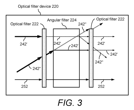
100101 FIG. 3 illustrates a block diagram of an optical filter device,
according to an
embodiment.
100111 FIG. 4 illustrate a block diagram of an optical filter device,
according to an
embodiment.
2
CA 03147294 2022-01-12
WO 2021/035047 PCT/US2020/04 7188
[0012] FIG. 5 illustrates a block diagram of an optical filter device,
according to an
embodiment.
[0013] FIG. 5 is a bar graph showing experimental results comparing the
emission-to-
excitation ratio of various optical filter configurations.
DETAILED DESCRIPTION
[0014] Embodiments described herein generally relate to an optical filter
device and/or
system and method for improved optical rejection of out-of-band wavelengths.
According to some
embodiments, an analyte detection system includes an excitation light source
for illuminating an
implantable sensor and an optical detector for collecting emission light from
the implantable
sensor. An optical filter device can be operable to reject out-of-band
wavelengths, for example
originating from the excitation light source, while allowing a signal of
interest, for example
originating from the implantable sensor, to be received by the optical
detector. According to some
embodiments, optical filter devices described herein can be operable to
provide high optical
rejection of out-of-band wavelengths of light from an optical band-pass filter
even when the
incident light on the filter is scattered light that strikes the surface of
the filter at angles of
incidence ranging from nearly +90 degrees to -90 degrees. Thus, optical filter
devices described
herein are capable of providing efficient optical filtering of uncollimated
fluorophore excitation
light from uncollimated fluorophore emission light in a simple, stray light-
insensitive, compact,
manufacturable form-factor that is suitable for use in, for example, a
wearable detection device.
[0015] An analyte detection system, according to some embodiments, include
an optical filter
device that includes one or more angular filters in combination with one or
more optical filters.
Optical filter devices described herein typically include at least three
layers (e.g., a stack of
bandpass and angular filters). Such optical filter devices are capable of
substantially rejecting the
excitation light signal while transmitting the emission light signal. In one
example, the optical
filter device includes, in order, a first angular filter, an optical bandpass
filter, and a second
angular filter. In another example, the optical filter device includes, in
order, a first optical
bandpass filter, an angular filter, and a second optical bandpass filter. In
yet another example, the
optical filter device includes, in order, a first angular filter, a first
optical bandpass filter, a second
angular filter, and a second optical bandpass filter.
3
CA 03147294 2022-01-12
WO 2021/035047 PCT/US2020/04 7188
[0016] Embodiments described herein can include an optical filter device
that can reject
excitation light at orders of magnitude greater than emission light power at
the worst-case angle
of incidence of the system.
[0017] In some embodiments, an analyte detection system that includes an
optical filter
device is implemented in a wearable detection device.
[0018] In some embodiments, an analyte detection system including an
optical filter device
can be physically scalable to incorporate into a wearable detection device.
Namely, the optical
filter device may be provided in a form factor that is suitable for a wearable
detection device.
[0019] Some embodiments described herein relate to a method that includes
subjecting a
diffuse optical signal to an optical filter device to reject components
associated with an excitation
light source, while passing components associated with an emission signal. An
excitation light
source can be operable to illuminate a sensor disposed in a highly scattering
environment, such
as tissue. The scattering environment can cause light from the excitation
source to scatter and
reflect back towards the excitation light source at a wide range of angles.
The sensor can be
operable to absorb a portion of the excitation light and emit the emission
signal at a different,
typically higher, wavelength. Light that exits the scattering environment (the
diffuse optical
signal) can therefore include components associated with the excitation light
source and
components associated with emissions from the sensor.
[0020] The method can include subjecting the diffuse optical signal to a
first angular filter to
produce a first filtered optical signal. The first angular filter can be
configured to reject
components of the diffuse optical signal that have an angle of incidence
outside a predefined
range (e.g., greater than 20 degrees and/or less than -20 degrees). Components
that pass the first
angular filter (e.g., a first filtered optical signal) can be subjected to a
bandpass filter that is
configured to reject components of the first filtered optical signal that that
have an angle of
incidence less than 30 degrees (and/or greater than -30 degrees) and a
wavelength shorter than a
first predefined thereshold. Components that pass the bandpass filter (e.g., a
second filtered
optical signal) can be subjected to a second angular filter that is configured
to reject components
of the second filtered optical signal that have an angle of incidence greater
than 20 degrees (and/or
less than -20 degrees). Components that pass the second angular filter (e.g.,
a third filtered optical
signal) can be sensed by a detector. The components sensed by the detector can
have a very high
signal to noise (or emission to excitation) ratio.
4
CA 03147294 2022-01-12
WO 2021/035047 PCT/US2020/04 7188
[0021] FIG. 1 is a block diagram an analyte detection system 100, according
to an
embodiment, that including an optical filter device providing high optical
rejection of out-of-band
wavelengths. The analyte detection system 100 and optical filter device can be
used for reading
an implantable sensor and determining an analyte value.
[0022] The analyte detection system 100 includes a detection device 110
that can be
positioned adjacent to an implantable sensor 150 implanted in tissue 105. For
example,
implantable sensor 150 may be implanted a few millimeters (e.g., 1-10 mm)
under the skin of the
user and the detection device 110 can be positioned outside the tissue and
over the implantable
sensor.
[0023] Implantable sensor 150 may be, for example, an analyte-sensing
fluorescent sensor.
When implanted in tissue 105, implantable sensor 150 is in good contact (close
proximity) to
blood vessels and has direct access to of interstitial fluid and can therefore
be operable to measure
various biological analytes. Implantable sensor 150 includes analyte-sensing
dye. The analyte-
sensing dye in implantable sensor 150 can be an analyte-specific dye for
targeting the analyte of
interest. Examples of analytes of interest may include, but are not limited
to, oxygen, reactive
oxygen species, glucose, lactate, pyruvate, cortisol, creatinine, urea,
sodium, magnesium,
calcium, potassium, vasopressin, hormones (e.g., Luteinizing hormone), pH,
CO2, cytokines,
chemokines, eicosanoids, insulin, leptins, small molecule drugs, ethanol,
myoglobin, nucleic
acids (RNAs, DNAs), fragments, polypeptides, single amino acids, and the like.
In one example,
implantable sensor 150 may be a glucose sensor and therefore the analyte-
sensing dye is a
glucose-sensing dye.
[0024] Detection device 110 is an optical device that includes an
excitation light source 140
operable to illuminate and excite the implantable sensor 150, an optical
detector 146 operable to
receive signals emitted by the implantable sensor 150, and an optical filter
device 120 that
provides high optical rejection (e.g., 10, le, or 10' optical rejection) of
out-of-band
wavelengths (e.g., noise associated with the excitation light source 140).
Detection device 110
further includes certain optical components 144 and a communications port 148.
In some
embodiments, detection device 110 may include a power source (not shown), such
as a battery.
Detection device 110 is designed to be fitted against the surface of the skin.
Detection device 110
may be implemented using a printed circuit board (PCB), a flexible PCB, or
other flexible
substrate. Detection device 110 may be, for example, a wearable detection
device provided as a
CA 03147294 2022-01-12
WO 2021/035047 PCT/US2020/04 7188
patch that can be placed on the surface of the skin (i.e., tissue 105) in
close proximity to
implantable sensor 150.
100251 Excitation light source 140 is arranged to transmit excitation light
142 from the surface
of the skin, through the tissue 105, and to implantable sensor 150. The
excitation light 142 from
excitation light source 140 is within the excitation wavelength range of any
analyte-sensing dye
of implantable sensor 150. Suitable excitation light sources may include, but
are not limited to,
lasers, semi-conductor lasers, light emitting diodes (LEDs), and organic LEDs.
Optical
components 144 may include any types of components (e.g., optical filters)
needed in detection
device 110 for conditioning excitation light source 140.
100261 The optical detector 146 is operable to detect emission light 152
from the analyte-
sensing dye of implantable sensor 150 that has passed through and exited the
tissue 105. Namely,
optical detector 146 detects emission light 152 in the emission wavelength of
the analyte-sensing
dye of implantable sensor 150. Suitable optical detectors may include, but are
not limited to,
photodiodes, complementary metal-oxide-semiconductor (CMOS) detectors, and
charge-coupled
device (CCD) detectors.
100271 As discussed in further detail herein, optical detector 146 can be
filtered using optical
filter device 120 such that the optical detector 146 is operable to measure
the optical signals
emitted within the desired wavelength ranges (e.g., the emission wavelength
range) and such that
optical filter device 120 provides high optical rejection of out-of-band
wavelengths (e.g., the
excitation wavelength band) the as compared with conventional optical
detection devices.
100281 In use, the implantable sensor 150 is excited at its excitation
wavelength via excitation
light 142. Then, implantable sensor 150 absorbs the excitation light 142 and
emits longer
wavelength emission light 152. Then, optical filter device 120 rejects the
excitation light 142
allowing for the emission light 152 to be measured accurately by optical
detector 146. As
discussed in further detail herein, however, because tissue is a highly
scattering environment,
portions of the excitation light 142 strike the optical filter device at a
wide range of angles of
incidence (e.g., from -89 degrees to 89 degrees). Known bandpass filters may
be ineffective to
discriminate between emission light 152 and high angle of incidence excitation
light. Optical filter
device 120, therefore, may include, for example, an arrangement or stack of
one or more optical
components.
6
CA 03147294 2022-01-12
WO 2021/035047 PCT/US2020/04 7188
100291 Detection device 110 can include built-in electronic processing
device(s) (not shown)
and/or data storage (not shown). In such embodiments, the processing
capability of analyte
detection system 100 can be completely or partially on board detection device
110 that is located
on the surface of the skin. In addition or alternatively, the processing
capability of analyte
detection system 100 is external to detection device 110 that is located on
the surface of the skin.
Accordingly, communications port 148 is provided between detection device 110
and a separate
computing device 160, wherein computing device 160 may be used for processing
any
information from detection device 110. Computing device 160 may be any type of
computing
device, such as a desktop computer, a laptop computer, a tablet device, a
mobile phone, a
smartphone, a centralized server or cloud computer, and the like. In this
example,
communications port 148 facilitates a wired and/or wireless communications
link from excitation
light source 140 and/or optical detector 146 to, for example, computing device
160. For example,
communications port 148 may be a wired communications port, such as a USB
port, and/or a
wireless communications port that uses, for example, WiFi and/or Bluetooth
technology.
[0030] Computing device 160 may use a desktop application 162 or mobile app
162 to process
any information from implantable sensor 150. Namely, desktop application 162
or mobile app
162 may include any software and/or hardware components for processing any
information from
implantable sensor 150. While detection device 110 may include battery power,
in other
embodiments, computing device 160 supplies power to detection device 110.
[0031] In one example, computing device 160 may be used to activate
excitation light source
140, wherein excitation light source 140 emits excitation light 142 and
illuminates the analyte-
sensing dye in implantable sensor 150, wherein the analyte-sensing dye has a
certain absorption
spectrum and a certain emission spectrum. Then, optical detector 146 collects
emission light 152
from implantable sensor 150 that passes through optical filter device 120 and
wherein optical
filter device 120 provides high optical rejection of out-of-band wavelengths
of emission light 152.
Then, computing device 160 collects information from optical detector 146,
wherein optical
detector 146 converts optical signals received from implantable sensor 150 to
an electrical signal
output. The measured intensity of emission light 152 correlates to an analyte
value. For example,
in an implantable glucose sensor 150 the measured intensity of emission light
152 (i.e.,
fluorescence) correlates to the amount or concentration of glucose present.
Generally, excitation
light 142 is orders of magnitude stronger than emission light 152.
Accordingly, optical filter
7
CA 03147294 2022-01-12
WO 2021/035047 PCT/US2020/04 7188
device 120 is used to separate excitation light 142 and emission light 152.
Namely, optical filter
device 120 is used to reject excitation light 142 as much as possible to
increase the signal-to-noise
ratio of light that illuminates the optical detector 146. As described in
further detail herein, the
optical filter device 120 is particularly well suited to efficiently reject
excitation light for
fluorophores with short stoke-shifts, even in highly scattering environments
such that the
acceptable range of angle of incidence on the optical filter device 120 is
higher than is possible
with known filtering techniques used for short stokes-shift fluorophores. For
example,
particularly for fluorophores where the excitation peak is very close to the
emission peak (e.g.,
50, 30, 25, or 15 nm or less) discriminating between an emission signal and
backscattered
excitation signal at an off-angle can be difficult using known filters and
filtering methods.
Embodiments described herein are capable of high optical rejection (e.g.,
greater than 10) of out-
of-band light at high angles of incidence (e.g., outside of +1- 30 degrees),
which may not
achievable according to known methods suitable for detecting short stoke-shift
emissions from
an implantable sensor.
100321 FIG. 2 is a block diagram of the detector device 110 shown and
described above with
reference to FIG. 1, showing additional details of the optical filter device
120. The optical power
of the excitation light source 140, configured to excite a fluorophore is
often orders (e.g., 1, 2, or
3) of magnitude stronger than the resulting fluorescence emission. Therefore,
it is desirable for
the optical filter device 120 to be designed to reject excitation light at
orders of magnitude greater
than emission light power at the worst-case angle of incidence of the system.
Namely, the cutoff
wavelengths (or filter window) for optical band-pass filters are often
dependent on the angle of
the incident light. As angle of incidence increases, the filter window shifts
to shorter wavelengths
(i.e., blue shifts). In the case of fluorophore excitation and emission, this
blue shift causes the
optical filter window for the emission to shift towards the excitation light
source, in some cases
rendering the optical band-pass filters ineffective (allowing greater than
50%, 75%, 90% etc. of
out-of band light to pass) at rejecting light in the excitation bandwidth
range that has a high angle
of incidence (e.g., outside of +1- 20, 25, 30, 35, 45 degrees). Accordingly,
optical filter device
120 of analyte detection system 100, which may rely on intensity-based
measurements, can be
operable to reject excitation light at orders of magnitude greater than
emission light power at the
worst-case angle of incidence of the system.
8
CA 03147294 2022-01-12
WO 2021/035047 PCT/US2020/04 7188
100331 FIG. 2 shows excitation light 142 striking implantable sensor 150.
Additionally,
excitation light 142 reaches the optical filter device 120 (e.g., due to
diffuse reflectance and/or
back scatter) across a wide range of angles of incidence (e.g., from -89
degrees to 89 degrees). In
response to excitation light 142, implantable sensor 150 produces emission
light 152. Typically
the optical detector 146 is positioned over the implantable sensor 150, such
that much of the
emission light 152 is substantially normal to optical filter device 120.
100341 As discussed in further detail herein, the optical filter device 120
is designed to reject
excitation light that is orders of magnitude more intense than emission light
power at the worst-
case angle of incidence of the system (e.g., +/- 89 degrees). Thus optical
filter device 120
substantially rejects excitation light 142 that reaches the optical filter
device at or near 0 degrees
angle of incidence (e.g., normal excitation light) and at high angles of
incidence, while at the
same time transmitting emission light 152. For example, the emission-to-
excitation ratio of
emission light 152-to-excitation light 142 at the output of optical filter
device 120 is large,
according to some embodiments > 200.
100351 Generally, the presently disclosed analyte detection system 100
provides an optical
filter device 120 that includes one or more angular filters in combination
with and alternating
with one or more optical filters in order to substantially reject the
excitation light signal and while
transmitting the emission light signal. The optical filter device 120
typically includes at least three
layers, as experimental results have demonstrated that two or few layers
provides dramatically
inferior rejection of out-of-band light. In some instances, as compared to a
two-layer optical filter
device, a three-layer optical filter device can increase the signal-to-noise
ratio by a factor of >350.
For example, as shown according to the embodiment depicted in FIG. 3, an
optical filter 220
includes, in order, a first optical filter 222, an angular filter 224, and a
second optical filter 222.
100361 Optical filter 220 allows filtering of out-of-band light from a
diffuse source (e.g.,
tissue). First and second optical filters 222 can be thin film optical
bandpass filters. First and
second optical filters 222 may be, for example, the 707 nm filter (p/n PROF-
0016) available from
Semrock, a unit of 1DEX Health & Science, LLC (Rochester, NY). An angular
filter allows
normal light (light striking the angular filter 224 at or near a 0 degree
angle of incidence, light
striking the angular filter 224 at an angle of incidence between +10 degrees
and -10 degrees, light
striking the angular filter 224 at an angle of incidence between +20 degrees
and -20 degrees, etc.)
to pass through while preventing light at high angle (e.g., light having an
angle of incidence
9
CA 03147294 2022-01-12
WO 2021/035047 PCT/US2020/04 7188
outside of 30 degrees) from passing through. Accordingly, angular filter 224
provides a certain
angular rejection of light. Angular filter 224 may be, for example, a fiber
optic plate (FOP). An
FOP is an optical device formed of a bundle of micron-diameter fibers. An FOP
directly conveys
light or image incident on its input surface to its output surface. Examples
of FOPs suitable for
optical filter device 220 may include, but are not limited to, the SCHOTT
Fiber Optic Faceplates
available from SCHOTT North America, Inc. (Southbridge, MA) and the FOPs
available from
Hamamatsu Corporation (Bridgewater, NJ). In another example, angular filter
224 may be series
of apertures.
[0037] While the aforementioned example components may be suitable for
glucose-specific
dye, more generally the components of optical filter device 220 may be:
Optical Filters:
Bandpass Wavelengths in the following range: 400nm ¨ 1600nm
Substrate: Glass, plastic, other transparent materials.
Optical Density(OD) outside of passband, specifically near excitation
wavelengths:
>40D
Optical Transmission in pass-band: >1%
Steep cut on/off edges: <30nm cutoff width
Fiber Optic Plates(FOP)
Numerical Aperature:0.5-0.05
Normal incident transmi ssi on : >1%
Stray Light Control: EMA glass or equivalent to prevent crosstalk between
fibers
High angle light rejection at: OD>4
Apertures (single or array)
High angle light rejection at: OD>4
Normal incident transmission: >1%
Lenses(single or array) + system of apertures
Numerical Aperture: 0.5-0.05
High angle light rejection at: OD>4
Normal incident transmission: >1%
CA 03147294 2022-01-12
WO 2021/035047 PCT/US2020/04 7188
[0038] In operation, the specifications (e.g., wavelength pass band) of
first optical filter 222,
angular filter 224, and second optical filter 222 are selected such that
emission light 252 (at a
predefined wavelength) passes through the arrangement in a substantially
unfiltered fashion and
such that excitation light 242 (at a different, lower, predefined wavelength)
is substantially
rejected. With respect to rejecting excitation light 242, both a normal
component of excitation
light 242 (e.g., normal excitation light 242') and a high angle component of
excitation light 242
(e.g., high angle excitation light 242") reaches optical filter device 220.
First optical filter 222
substantially filters out normal excitation light 242' such that a negligible
amount (e.g., >10-5, 10-
6, le') of normal excitation light 242' passes down the line and reaches the
output of optical filter
device 220. However, high angle excitation light 242" (e.g., light having an
angle of incidence
greater than 25, 30, 35, 45, degrees, etc. and/or less than -25, -30, -35, -45
degrees etc.) passes
through first optical filter 222 and reaches angular filter 224. Similarly
stated, the first optical
filter 222 may be ineffective (may be operable to reject less than 50% of)
light within the
excitation bandwidth range that strikes the first optical filter 222 at high
angles of incidence.
Angular filter 224 substantially filters out high angle excitation light 242"
such that a negligible
amount of high angle excitation light 242" passes down the line and reaches
the output of optical
filter device 220. However, when high angle excitation light 242" reaches the
interface of angular
filter 224 a new normal excitation light 242' component may be formed that
passes on to second
optical filter 222. Second optical filter 222 substantially filters out this
normal excitation light
242' such that only a negligible amount thereof reaches the output of optical
filter device 220. In
this manner, optical filter device 220 is used to substantially reject any
normal and high angle
components of excitation light 242 while transmitting emission light 252.
[0039] According to another embodiment shown in FIG. 4, an optical filter
device 320
includes, in order, a first angular filter 324, a first optical bandpass
filter 322, a second angular
filter 326, and a second optical bandpass filter 328. Namely, optical filter
device 320 shown in
FIG. 4 is substantially the same as optical filter device 320 shown in FIG. 3
except for the addition
of another angular filter 324 in advance of the first optical bandpass filter
322. First angular filter
324 provides an additional level of filtration. For example, to achieve a
certain desired level of
optical rejection, additional stages (e.g., first angular filter 324) can be
added to increase
performance.
11
CA 03147294 2022-01-12
WO 2021/035047 PCT/US2020/04 7188
[0040] According to another embodiment shown in FIG. 5, an optical filter
device 420
includes, in order, a first angular filter 424, an optical bandpass filter
422, and a second angular
filter 426. Namely, optical filter device 420 shown in FIG. 5 is substantially
the same as optical
filter device 320 shown in FIG. 3 except instead of two optical filters and
one angular filter,
optical filter device 420 includes two angular filters 424, 426 and one
optical filter 422.
[0041] Optical filter devices are not limited to the number and order of
components shown
with reference to FIG. 3 - 5. These configurations are exemplary only. An
optical filter device
may include any number of one or more angular filters in combination with two
or more optical
filters and in any order to substantially reject the excitation light signal
while transmitting the
emission light signal. Frequently, but not necessarily, angular filters and
optical filters alternate
in the stack of the optical filter device. However, there may be a balance of
the number and
arrangement of components without reducing significantly the signal-to-noise
(SNR) of optical
filter device.
[0042] An embodiment includes a wearable detection device which includes a
housing
bottom and a housing top. A housing bottom may include a housing window,
wherein housing
bottom is the portion of wearable detection device that is placed against the
user's skin. In an
aspect, a temperature detector may be included to detect the temperature of
the user's skin. The
wearable detection device may include a main printed circuit board (PCB) and a
skin temp PCB,
wherein skin temp PCB may be in thermal contact with the temperature detector
and may process
skin temperature information from the temperature detector. The main PCB may
include a
plurality of LEDs and an optical detector. The optical detector is one example
of optical detector
146 shown in FIG. 1 and FIG. 2.
[0043] In an embodiment, the wearable detection device may also include a
processor, which
may be the master controller that is used to manage the overall operations of
wearable detection
device. The processor may be any standard controller or microprocessor device
that is capable of
executing program instructions. Further, a certain amount of data storage may
be associated with
the processor. The main PCB may include any other components that may be
useful in wearable
detection device, such as, but not limited to, a communications interface. In
one example,
wearable detection device can be used to report out the user's glucose level
periodically, such as
every few minutes.
12
CA 03147294 2022-01-12
WO 2021/035047 PCT/US2020/04 7188
[0044] In an embodiment, the wearable detection device may include a first
dual bandpass
filter (e.g., configured to pass optical signals associated with multiple
fluorescent dyes having
different emission spectra), a first FOP, a second dual bandpass filter, and a
second FOP, which
may be arranged in a stack. This stack of first dual bandpass filter, first
FOP, second dual bandpass
filter, and second FOP is one example of the presently disclosed optical
filter device 120 that
provides high optical rejection of out-of-band wavelengths. More particularly,
this stack is one
example of optical filter device 320 shown in FIG. 4. Namely, dual bandpass
filters is an example
of an optical filter(s) 322, 328 of optical filter device 320 of FIG. 4 and
FOPs are an example of
an angular filter(s) 324, 326 of optical filter device 320 of FIG. 4.
[0045] In an embodiment, the wearable detection device may include a
battery for supplying
power to the active components thereof The battery may be a rechargeable or
non-rechargeable
battery.
[0046] In one example, the wearable detection device has an overall length
of about 3 cm,
and overall width of about 2 cm, and an overall thickness or height of about 1
cm. Each of the
dual bandpass filters may be, for example, about 1 mm thick. Each of the FOPs
may be, for
example, from about 0.5 mm to about 1 mm thick. Accordingly, the entire stack
may be, for
example, from about 2 mm to about 4 mm thick. Additionally, the stack may be,
for example,
about 4 mm square. In one example, the wearable detection device may be held
on the user's skin
using an adhesive patch. The housing window of the wearable detection device
may be positioned
in relation to an implantable sensor, such as implantable sensor 150, in order
to capture optical
readings therefrom.
[0047] In other embodiments, instead of using discrete components, such as
the stack of dual
bandpass filters and FOPs, optical filter device 120 and optical detector 146
can be provided as
an integrated component formed entirely using silicon manufacturing methods.
For example, an
optical detector is provided at the wafer and die level. Then, at the wafer
level, the die are coated
with a filter material. Then, a series of lenses or angular filters are
deposited on the filter. Then,
the wafer is diced to form individual integrated circuit (IC) devices that
include both optical filter
device 120 and optical detector 146.
[0048] FIG. 6 illustrates an example of a bar graph 300 comparing the
emission-to-excitation
ratio of various optical filter configurations including the presently
disclosed optical filter device
120. Bar 510 illustrates the performance of the optical filter device 220,
shown and described
13
CA 03147294 2022-01-12
WO 2021/035047 PCT/US2020/04 7188
with reference to FIG. 3. With a emission-to-excitation (signal-to-noise)
ratio in excess of 200,
FIG. 6 illustrates the dramatic performance improvement (more than 350 times
better) than some
known filter devices, that may only include two layers (bar 512). The
experimental data for the
an optical filter configuration including an FOP as a collimator to collimate
the light prior to the
light striking an optical bandpass filter, shown in bar 314 shows improved
performance relative
to non-collimated light, but inferior to the optical filter device 222 (bar
510).
[0049] Following long-standing patent law convention, the terms "a," "an,"
and "the" refer
to "one or more" when used in this application, including the claims. Thus,
for example, reference
to "a subject" includes a plurality of subjects, unless the context clearly is
to the contrary (e.g., a
plurality of subjects), and so forth.
[0050] Throughout this specification and the claims, the terms "comprise,"
"comprises," and
"comprising" are used in a non-exclusive sense, except where the context
requires otherwise.
Likewise, the term "include" and its grammatical variants are intended to be
non-limiting, such
that recitation of items in a list is not to the exclusion of other like items
that can be substituted
or added to the listed items.
[0051] For the purposes of this specification and appended claims, unless
otherwise indicated,
all numbers expressing amounts, sizes, dimensions, proportions, shapes,
formulations,
parameters, percentages, quantities, characteristics, and other numerical
values used in the
specification and claims, are to be understood as being modified in all
instances by the term
"about" even though the term "about" may not expressly appear with the value,
amount or range.
Accordingly, unless indicated to the contrary, the numerical parameters set
forth in the following
specification and attached claims are not and need not be exact, but may be
approximate and/or
larger or smaller as desired, reflecting tolerances, conversion factors,
rounding off, measurement
error and the like, and other factors known to those of skill in the art
depending on the desired
properties sought to be obtained by the presently disclosed subject matter.
For example, the term
"about," when referring to a value can be meant to encompass variations of, in
some embodiments
100%, in some embodiments 50%, in some embodiments 20%, in some
embodiments
10%, in some embodiments 5%, in some embodiments 1%, in some embodiments
0.5%,
and in some embodiments 0.1% from the specified amount, as such variations
are appropriate
to perform the disclosed methods or employ the disclosed compositions.
14
CA 03147294 2022-01-12
WO 2021/035047 PCT/US2020/04 7188
100521 Further, the term "about" when used in connection with one or more
numbers or
numerical ranges, should be understood to refer to all such numbers, including
all numbers in a
range and modifies that range by extending the boundaries above and below the
numerical values
set forth. The recitation of numerical ranges by endpoints includes all
numbers, e.g., whole
integers, including fractions thereof, subsumed within that range (for
example, the recitation of 1
to 5 includes 1, 2, 3, 4, and 5, as well as fractions thereof, e.g., 1.5,
2.25, 3.75, 4.1, and the like)
and any range within that range.
100531 Some embodiment describe filtering as being "effective" or
"ineffective." In some
instances, a filter is "effective" against (or "configured to reject") a
particular signal if it blocks
>99.99% (104 rejection) of that signal. In other instances, an effective
filter provides 10-5 or 10-
' rejection of out-of-band photons. Conversely, in some instances, a filter is
ineffective against a
particular signal if it allows more than 0.5%, 0.01%, 0.001% or 0.00001% of
that signal to pass.
100541 Although the foregoing subject matter has been described in some
detail by way of
illustration and example for purposes of clarity of understanding, it will be
understood by those
skilled in the art that certain changes and modifications can be practiced
within the scope of the
appended claims. Furthermore, although various embodiments have been described
as having
particular features and/or combinations of components, other embodiments are
possible having a
combination of any features and/or components from any of embodiments where
appropriate as
well as additional features and/or components.
[0055] Where methods described above indicate certain events occurring in
certain order, the
ordering of certain events may be modified. Additionally, certain of the
events may be performed
concurrently in a parallel process when possible, as well as performed
sequentially as described
above. Although various embodiments have been described as having particular
features and/or
combinations of components, other embodiments are possible having a
combination of any
features and/or components from any of the embodiments where appropriate.