Note: Descriptions are shown in the official language in which they were submitted.
WO 2021/034916
PCT/US2020/046970
STRUCTURED ANODES FOR LITHIUM-BASED ENERGY STORAGE
DEVICES
CROSS REFERENCE TO RELATED APPLICATION
This application claims the benefit of priority of U.S. Provisional
Application No.
62/889,351, filed August 20, 2019, which is incorporated herein by reference
in its entirety for
all purposes.
TECHNICAL FIELD
The present disclosure relates to lithium ion batteries and related energy
storage devices.
BACKGROUND
Silicon has been proposed as a potential material for lithium-ion batteries to
replace the
conventional carbon-based anodes which have a storage capacity that is limited
to ¨370 mAh/g.
Silicon readily alloys with lithium and has a much higher theoretical storage
capacity (-3600 to
4200 inAh/g at room temperature) than carbon-based anodes. However, insertion
and extraction
of lithium into the silicon matrix causes significant volume expansion (>300%)
and contraction.
This can result in rapid pulverization of the silicon into small particles and
electrical
disconnection from the current collector.
The industry has recently turned its attention to nano- or micro-structured
silicon to
reduce the pulverization problem, i.e., silicon in the form of spaced apart
nano- or micro-wires,
tubes, pillars, particles, and the like. The theory is that making the
structures nano-sized avoids
crack propagation and spacing them apart allows more room for volume
expansion, thereby
enabling the silicon to absorb lithium with reduced stresses and improved
stability compared to,
for example, macroscopic layers of bulk silicon.
Despite research into structured silicon approaches, such batteries based
primarily on
silicon have yet to make a large market impact due to unresolved problems.
SUMMARY
There remains a need for anodes for lithium-based energy storage devices such
as Li-ion
batteries that are easy to manufacture, robust to handling, high in charge
capacity and amenable
to fast charging, for example, at least 1C These and other needs are addressed
by the
embodiments described herein.
In accordance with an embodiment of this disclosure, an anode for an energy
storage
device is provided that includes a current collector and a lithium storage
coating. The current
1
CA 03148530 2022-2-17
WO 2021/034916
PCT/US2020/046970
collector includes: i) an electrically conductive substrate including a fffst
electrically conductive
material; a plurality of electrically conductive structures
in electrical communication with the
electrically conductive substrate, wherein each electrically conductive
structure includes a
second electrically conductive material; and iii) a metal oxide coating. The
metal oxide coating
includes one or both of: a) a first metal oxide material in contact with the
electrically conductive
substrate; or b) a second metal oxide material in contact with the
electrically conductive
structures; or both (a) and (b). The anode further includes lithium storage
coating overlaying the
metal oxide coating, the lithium storage layer including a total content of
silicon, germanium, or
a combination thereof, of at least 40 atomic %. The electrically conductive
structures are at least
partially embedded within the lithium storage coating.
The present disclosure provides anodes for energy storage devices that may
have one or
more of at least the following advantages relative to conventional anodes:
improved stability at
aggressive >IC charging rates; higher overall areal charge capacity; higher
charge capacity per
gram of silicon; improved physical durability; simplified manufacturing
process; and more
reproducible manufacturing process.
BRIEF DESCRIPTION OF DRAWINGS
FIGS. 1 A ¨ IC are cross-sectional views illustrating the making of an anode
according to
some embodiment of the present disclosure.
FIGS. 2A ¨ 2E are cross-sectional views illustrating the making of an anode
according to
some embodiment of the present disclosure.
FIGS. 3A ¨ 2C are cross-sectional views illustrating the making of an anode
according to
some embodiment of the present disclosure.
FIGS. 4A ¨ 4C are cross-sectional views illustrating the making of an anode
according to
some embodiment of the present disclosure.
FIG. 5A is a plan view of a current collector precursor according to some
embodiment of
the present disclosure.
FIG. 5B is a cross-sectional view of a current collector precursor taken along
cut line B-B
of FIG. 5A.
FIG. 5C is a cross-sectional view of a current collector precursor taken along
cut line C-C
of FIG. 5A.
2
CA 03148530 2022-2-17
WO 2021/034916
PCT/US2020/046970
FIGS. 6A ¨ 6F are cross-sectional views of current collector precursors
illustrating
various shapes available for the electrically conductive structures according
to some
embodiments of the present disclosure.
FIG. 7 is a plan view of a current collector precursor illustrating various
shapes for the
electrically conductive structures according to some embodiments of the
present disclosure.
FIG. 8 is a schematic cross-sectional view of a battery according to some
embodiments of
the present disclosure.
DETAILED DESCRIPTION
It is to be understood that the drawings are for purposes of illustrating the
concepts of the
disclosure and may not be to scale. Various aspects of anodes of the present
disclosure, including
metal oxide layers, deposition of lithium storage material, additional layers
and methods are
described in co-pending US patent application nos. 16/285,842, 16/909,008,
16/991,613,
16/991,623, and 16/991,626, the entire contents of which are incorporated by
reference for all
purposes.
Anode Overview
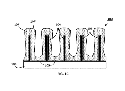
FIGS. lA - 1C are cross-sectional views illustrating the fabrication of an
anode
according to some embodiments of the present disclosure. In FIG. 1A, a current
collector
precursor 101' includes an electrically conductive substrate 103 and a
plurality of electrically
conductive structures 104 in electrical communication with the electrically
conductive substrate
103, for example, through direct physical contact. The electrically conductive
substrate 103
includes a first electrically conductive material and each of the plurality of
electrically
conductive structures comprises a second electrically conductive material,
which may be the
same as, or different than, the first electrically conductive material,
Materials, methods of
making, and other features of the current collector precursor 101' are
discussed later.
In FIG. 1B, a metal oxide coating is provided in contact with the current
collector
precursor 101' to form current collector 101. In the present embodiment, the
metal oxide coating
includes a first metal oxide material 105 formed in contact with the
electrically conductive
substrate 103 and a second metal oxide material 106 formed in contact with
electrically
conductive structures 104. In some embodiments, the first metal oxide material
is provided as a
coating or layer over most of the available surface area of the electrically
conductive substrate
3
CA 03148530 2022-2-17
WO 2021/034916
PCT/US2020/046970
not otherwise occupied by the electrically conductive structures. Materials,
methods of forming,
and other features of the metal oxide material are discussed later.
In FIG. 1C, a lithium storage coating 107 having an outer surface 107' is
deposited over
the current collector 101 and in contact with the metal oxide coating (the
first metal oxide
material 105 and second metal oxide material 106) to form anode 100. The
electrically
conductive structures 104 are at least partially embedded within the lithium
storage coating 107.
That is, the lithium storage coating includes a plurality of concavities with
an electrically
conductive structure present in each concavity. As shown in FIG. 1C, the
electrically conductive
structures 104 may be fully embedded within the lithium storage coating 107.
In some
embodiments, as discussed later, the lithium storage coating may include
porous silicon
deposited by a CVD process, for example, a PECVD process. In some embodiments,
the
thickness of the lithium storage coating may be characterized by the distance
between the lithium
storage coating outer surface 107' to the nearest metal oxide material. The
thickness may vary
along the structure.
FIGS. 2A ¨ 2C are cross-sectional views illustrating the fabrication of an
anode
according to some embodiments of the present disclosure. In FIG 2A, a current
collector
precursor 201' includes an electrically conductive substrate 203 and a
plurality of electrically
conductive structures 204 in electrical communication with the electrically
conductive substrate
203, for example, through direct physical contact. The electrically conductive
substrate 203
includes a first electrically conductive material and each of the plurality of
electrically
conductive structures comprises a second electrically conductive material,
which may be the
same as, or different than, the first electrically conductive material.
Materials, methods of
making, and other features of the current collector precursor 201' are
discussed later.
In FIG. 2B, a metal oxide coating is provided in contact with the current
collector
precursor 201' to form current collector 201. In the present embodiment, the
metal oxide coating
includes a second metal oxide material 206 formed in contact with electrically
conductive
structures 204. Unlike FIG 1, there is no substantial amount metal oxide
(e.g., less than 0.01 Elm
thick if any at all) in contact with the electrically conductive substrate.
Materials, methods of
forming, and other features of the metal oxide material are discussed later.
In FIG. 2C, a lithium storage coating 207 may be deposited to form anode 200.
The
lithium storage coating 207 may overlay and be in contact with the second
metal oxide material
4
CA 03148530 2022-2-17
WO 2021/034916
PCT/US2020/046970
206. The electrically conductive structures 204 may be at least partially
embedded within the
lithium storage coating 207. The electrically conductive structures 204 may be
fully embedded
within the lithium storage coating 207. In some embodiments, as discussed
later, the lithium
storage coating may include porous silicon deposited by a CVD process, for
example, a PECVD
process. In some embodiments, as shown in FIG. 2C, the lithium storage coating
may selectively
deposit on the second metal oxide material 206 and does not form an adherent
coating over the
electrically conductive substrate In some embodiments, the rate of CVD
reaction may be faster at
the second metal oxide material surface than at the electrically conductive
substrate surface and
may continue to be faster at the surface of the lithium storage coating than
at the electrically
conductive substrate.
In some embodiments, as shown in FIG. 2D, anode 200D is formed where some
lithium
storage material may also deposit onto the bare electrically conductive
substrate, for example, as
a lithium storage layer 209, which may have a similar composition to lithium
storage coating
207. In some embodiments, the electrically conductive structures and lithium
storage coating 207
may physically assist in holding the lithium storage layer 209 between such
structures in place to
maintain adherence and electrical continuity with the electrically conductive
substrate.
In some embodiments, as shown in FIG. 2E, anode 200E is formed where a
plurality of
lithium storage nanostructures 208 may be formed on the electrically
conductive substrate
concurrently with deposition of the lithium storage coating 207 over the
second metal oxide. For
example, silicon-containing nanowires and microwires can be grown from nickel-
containing
electrically conductive substrates. In some embodiments, the nanowires and
microwires may
have a nickel silicide core and an amorphous silicon shell. Some non-limiting
methods of
growing lithium storage filaments on metals are described in US9325014 and
US8257866, the
entire contents of which are incorporated by reference for all purposes.
FIGS. 3A ¨ 3C are cross-sectional views illustrating the fabrication of an
anode
according to some embodiments of the present disclosure. In FIG. 3A, a current
collector
precursor 301' includes an electrically conductive substrate 303 and a
plurality of electrically
conductive structures 304 in electrical communication with the electrically
conductive substrate
303, for example, through direct physical contact. The electrically conductive
substrate 303
includes a first electrically conductive material and each of the plurality of
electrically
conductive structures comprises a second electrically conductive material,
which may be the
CA 03148530 2022-2-17
WO 2021/034916
PCT/US2020/046970
same as, or different than, the first electrically conductive material.
Materials, methods of
making, and other features of the current collector precursor 301' are
discussed later.
In FIG. 3B, a metal oxide coating is provided in contact with the current
collector
precursor 301' to form current collector 301. In the present embodiment, the
metal oxide coating
includes a first metal oxide material 305 formed in contact with the
electrically conductive
substrate 303. Unlike FIG. 1, there is no substantial amount of metal oxide
coating (e.g., less
than 0.002 pm thick if any at all) in contact with electrically conductive
structures 304. In some
embodiments, the first metal oxide material is provided as a coating or layer
over most of the
available surface area of the electrically conductive substrate not otherwise
occupied by the
electrically conductive structures. Materials, methods of forming, and other
features of the metal
oxide material are discussed later.
In FIG. 3C, a lithium storage coating 307 is deposited over the current
collector 301 and
in contact with the fffst metal oxide material 305 to form anode 300. The
electrically conductive
structures 304 are at least partially embedded within the lithium storage
coating 307. That is, the
lithium storage coating includes a plurality of concavities with an
electrically conductive
structure present in each concavity. As shown in FIG. 3C, the electrically
conductive structures
304 may be fully embedded within the lithium storage coating 307. In some
embodiments, as
discussed later, the lithium storage coating may include porous silicon
deposited by a CVD
process, for example, a PECVD process. In some embodiments, as shown in FIG.
3C, the lithium
storage coating may selectively deposit on the first metal oxide material 305
and does not form
an adherent coating over the electrically conductive structures. In some
embodiments, the rate of
the CVD reaction may be faster at the first metal oxide material surface than
at the electrically
conductive structures and may continue to be faster at the surface of the
lithium storage coating
than at the electrically conductive structures.
FIGS. 4A ¨C are cross-sectional views according to some embodiments of the
present
disclosure. In FIG 4A, current collector 401 includes an electrically
conductive substrate 403,
and a plurality of electrically conductive structures 404 in electrical
communication with
electrically conductive substrate 403. A first metal oxide material 405 is in
contact with
electrically conductive substrate 403 in regions not occupied by the
electrically conductive
structures 404.
6
CA 03148530 2022-2-17
WO 2021/034916
PCT/US2020/046970
In FIG. 413, a lithium storage coating 407 may be deposited to form anode
400B. The
lithium storage coating 407 may overlay and be in contact with the first metal
oxide material
405. The electrically conductive structures 404 are partially embedded within
the lithium storage
coating 407, but also extend beyond the lithium storage coating. In some
embodiments, as
discussed later, the lithium storage coating may include porous silicon
deposited by a CVD
process, for example, a PECVD process. In some embodiments, the lithium
storage coating
selectively deposits on the first metal oxide material 405. In some
embodiments, the rate of a
CVD reaction may be faster at the first metal oxide material surface than at
the electrically
conductive structures and may continue to be faster at the surface of the
lithium storage coating
than at the electrically conductive structure.
In some embodiments and as shown in FIG. 4C, after forming anode 400B,
deposition
conditions may be altered (for example, temperature may be increased) to
induce growth of
lithium storage filaments 408 on the electrically conductive structures 404,
forming hybrid anode
400C having both a lithium storage coating(s) and lithium storage filaments.
For example,
silicon-containing nanowires and microwires can be grown on nickel-containing
electrically
conductive structures. In some embodiments, the nanowires and microwires may
have a nickel
silicide core and an amorphous silicon shell. Some non-limiting methods of
growing lithium
storage filaments are described in US9325014 and US8257866, the entire
contents of which are
incorporated by reference for all purposes. Additional lithium storage coating
material may also
deposit over the first metal oxide material 405 while the lithium storage
filaments are growing.
Current Collector
In some embodiments, the electrically conductive substrate includes a first
electrically
conductive material. The first electrically conductive material may have a
conductivity of at least
100 Sim, alternatively at least 103 S/m, alternatively at least 106 S/m,
alternatively at least 107
S/m, In some embodiments, the first electrically conductive material may
include a metal. In
some embodiments, the metal may be a transition metal or an alloy including a
transition metal.
In some embodiments, the transition metal is copper, nickel, iron, chromium,
or titanium. In
some embodiment, the first electrically conductive material may include
stainless steel. In some
embodiments, the first electrically conductive material includes an
electrically conductive
carbon, such as carbon black, carbon nanotubes, graphene, graphene oxide,
reduced graphene
oxide, and graphite. In some embodiments the electrically conductive substrate
may be in the
7
CA 03148530 2022-2-17
WO 2021/034916
PCT/US2020/046970
form of a mesh or some other 3-dimensional structure, a foil or a sheet of
conductive material, or
a layer deposited onto an insulating substrate (e.g., a polymer sheet or
ceramic sheet coated with
conductive material such as nickel or copper, optionally on both sides).
In some embodiments, the electrically conductive substrate includes a mesh or
sheet of
electrically conductive carbon, including but not limited to, those formed
from bundled carbon
nanotubes or nanofthers. In some embodiments, such carbon-based electrically
conductive
substrates may include a surface layer of a conductive metal, e.g., nickel,
copper, zinc, titanium,
or the like. In some embodiments, the conductive metal surface layer may be
applied by
electrolytic or electroless plating methods.
In some embodiments, the electrically conductive substrate has an average
thickness of at
least 0.1 pm, alternatively at least 1 pm, alternatively at least 5 pm. In
some embodiments, the
electrically conductive substrate has an average thickness in a range of 0.1
pm to 1 pm,
alternatively 1 pm to 2 pm, alternatively 2 pm to 5 pm, alternatively 5 pm, to
10 pm,
alternatively 10 pm to 15 pm, alternatively 15 pm to 20 pm, alternatively 20
pm to 30 pm,
alternatively 30 pm to 50 pm, alternatively 50 pm to 100 pm, or any
combination of contiguous
ranges thereof
Referring to FIG. 5A, there is a plan view of current collector precursor 501'
having a
plurality of electrically conductive structures 504 in electrical
communication (e.g. in contact)
with electrically conductive substrate 503. Each of the plurality of
electrically conductive
structures 504 is characterized by a height H measured from the electrically
conductive substrate
503 to its end along a first electrically conductive structure axis. The
electrically conductive
structures may be further characterized by a width W and a length L, measured
parallel to the
electrically conductive substrate surface. In some embodiments, length L is
approximately the
same as W, and may be measured in a direction approximately orthogonal to the
width. FIG. 5B
shows a cross-sectional view of current collector precursor 501' along cut
line B-B to illustrate
H and W of electrically conductive structure 504. FIG. 5C shows a cross-
sectional view of
current collector precursor 501' along cut line C-C to illustrate H and L of
the electrically
conductive structure 504. In general, W represents the shortest dimension of
electrically
conductive structure 504 in plan view (FIG. 5A) and corresponds to the widest
portion of its
cross-section (FIG. 5B).
8
CA 03148530 2022-2-17
WO 2021/034916
PCT/US2020/046970
The electrically conductive structures may each have an aspect ratio defined
by height 11
divided by width W that is generally at least 1, alternatively at least 2,
alternatively at least 5,
alternatively at least 10. In some embodiments, the aspect ratio may be in a
range of 1 to 2,
alternatively 2 to 5, alternatively 5 to 10, alternatively 10 to 20,
alternatively 20 to 50,
alternatively 50 to 100, alternatively 100 to 200, alternatively 200 to 500,
alternatively in a range
of 500 to 1000, or any combination of contiguous ranges thereof There is no
particular
limitation on the length L of the electrically conductive structure other than
it is by definition at
least the same as width W, or greater. Referring again to FIG. 5A, a portion
of the surface area of
the electrically conductive substrate is in occupied by or in contact with the
electrically
conductive structures ("occupied area"). In some embodiments, the occupied
area is at least 1 %
and less than 99%. In some embodiments, the occupied area is in a range of 2%
to 10%,
alternatively 10% to 20%, alternatively 20% to 30%, alternatively 30% to 40%,
alternatively
40% to 50%, alternatively 50% to 60%, alternatively 60% to 70%, alternatively
70% to 80%,
alternatively 80% to 90%, alternatively 90% to 98%, or any combination of
contiguous ranges
thereof
In some embodiments, the surface area of the electrically conductive substrate
includes 2
to 5 electrically conductive structures per square centimeter, alternatively 5
to 10, alternatively
to 50, alternatively 50 to 100, alternatively 100 to 500, alternatively 500 to
1000, alternatively
1000 to 10,000, alternatively 5000 to 10,000, alternatively 10,000 to 100,000,
alternatively
100,000 to 1,000,000, alternatively 1,000,000 to 10,000,000 electrically
conductive structures, or
an any combination of contiguous ranges thereof. In some embodiments, the
surface area of the
electrically conductive substrate includes at least 5 electrically conductive
structures per square
centimeter, alternatively at least 10, alternatively at least 100,
alternatively at least 1000,
alternatively at least 10,000, alternatively at least 100,000, or
alternatively at least 1,000,000
electrically conductive structures.
In some embodiments, the height H of each of the plurality the electrically
conductive
structures may be at least 1 pm, alternatively at least 5 pm, alternatively at
least 10 pm,
alternatively at least 20 pm. In some embodiments, the average height H of the
electrically
conductive structures is in a range of 1 pm to 2 pm, alternatively 2 pm to 5
pm, alternatively 5
pm to 10 pm, alternatively 10 pm to 15 pm, alternatively 15 pm to 20 pm,
alternatively 20 pm
to 50 pm, alternatively 50 pm to 100 pm, or any combination of contiguous
ranges thereof In
9
CA 03148530 2022-2-17
WO 2021/034916
PCT/US2020/046970
some embodiments, the electrically conductive structure has a cross-sectional
width of at least
0.002 pm, alternatively at least 0.005 pm, alternatively at least 0.010 pm,
alternatively at least
0.10 pm, alternatively at least 1.0 pm, alternatively at least 10 pm,
alternatively at least 20 pm.
There are a wide variety of shapes the electrically conductive structures may
take,
including but not limited to, wires, pillars, tubes, ridges, or dendrites.
FIGS. 6A ¨ 6H illustrate
cross-sectional views of some non-limiting examples of electrically conductive
structures 604-a
¨ 604-h provided over electrically conductive substrate 603-a¨ 603-h. Height H
and width W
are also noted. In FIG. 6A, the electrically conductive structures 604-a may
have a triangular
shape in cross-section. Such structures may for example may be conical or
pyramidal. In FIG.
6B, the electrically conductive structures 604-b may have a trapezoidal shape
in cross-section. In
FIG. 6C, the electrically conductive structures 604-c may have an inverted
trapezoidal shape in
cross-section. In FIG. 6D, the electrically conductive structures 604-d may
have a circular, oval,
or ellipsoidal shape in cross-section. In FIG. 6E, the electrically conductive
structures 604-e may
have a right-triangular or wedge shape in cross-section. In FIG. 6F, the
electrically conductive
structures 604-f may have a base-and-pillar shape in cross-section. With a
base-and-pillar shape,
the aspect ratio may be in terms of the pillar width instead of the base
width. In FIG. 66,
electrically conductive structures 604-g may have a dendritic or branched
shape in cross section.
For such structures, W is defined by the maximum width of a branch or "trunk"
(the portion in
contact with the electrically conductive substrate), not the spread of
branches. In FIG. 611,
electrically conductive structures 604-h may have an irregular or nodular
shape in cross-section.
FIG. 7 illustrates a plan view of some additional non-limiting examples of
variously-
shaped electrically conductive structures 704-a ¨ 704-k, over electrically
conductive substrate
703 that may make up current collector precursor 701' For convenience only one
example of
each electrically conductive structure is shown. A current collector precursor
may include just
one type of shape or a plurality of shapes. The cross-sectional views of FIG 6
may be combined
with almost any of the structures of FIG. 7. The plan view shapes may appear
circular (704-a),
oblong or elliptical (704-b), polygonal such as hexagonal (704-e), square (704-
d), branched or
dendritic (704-e), tubular (704-0, crescent (704-g), intersected such as a
cross (704-h) or as part
of an interconnected mesh (7041), or as a long ridge, that may be straight
(704-j) or sinusoidal
(704-k). In some embodiments, when the electrically conductive structures are
oblong or ridge-
CA 03148530 2022-2-17
WO 2021/034916
PCT/US2020/046970
like, they may be provided parallel to an axis of winding, e.g., when
assembling jelly-roll type
batteries in in roll-to-roll manufacturing methods.
The electrically conductive structures may include a second electrically
conductive
material that may be substantially the same as or different than the first
electrically conductive
material. In some embodiments, when the electrically conductive material
includes a metal
"substantially the same as" may mean that the atomic % of each element of the
first electrically
conductive material is within 2 atomic % of the second electrically conductive
material. In some
embodiments, when the electrically conductive materials include conductive
carbon materials,
"substantially the same" may mean that the weight % of each form of conductive
carbon material
of the first electrically conductive material is within 2 weight % of each
form of conductive
carbon material in the second electrically conductive material. The second
electrically
conductive material may have a conductivity of at least 1 S/m, alternatively,
at least 10 S/m,
alternatively at least 100 S/m, alternatively at least 103 S/m, alternatively
at least 106 S/m,
alternatively at least 107 S/m, In some embodiments, the conductivity of the
second electrically
conductive material is lower than the conductivity of the first electrically
conductive material. In
some embodiments, the second electrically conductive material may include a
metal. In some
embodiments, the metal may be a transition metal or an alloy including a
transition metal. In
some embodiments, the transition metal is copper, nickel, iron, chromium, or
titanium. In some
embodiments, the second electrically conductive material may include a metal
suicide. In some
embodiment, the second electrically conductive material includes an
electrically conductive
carbon, such as carbon black, carbon nanotubes, graphene, graphene oxide,
reduced graphene
oxide, and graphite. In some embodiments, the electrically conductive
structures include carbon
nanotubes. In some embodiments, the carbon nanotubes may be embedded in the
electrically
conductive substrate, for example, as disclosed in US patents US 9,257,704 or
US 10,008,717,
the entire contents are incorporated herein for all purposes. In some
embodiments, the second
electrically conductive material may include a an electrically conductive
doped oxide, including
but not limited to, indium-doped tin oxide (ITO) or an aluminum-doped zinc
oxide (AZO).
In some embodiments, electrically conductive metal structures may be pattern
deposited
over an electrically conductive substrate by a PVD method such as evaporation
through a
shadow mask. In some embodiments metallic electrically conductive structures
may be
electrolytically or electrolessly plated through a patterned resist (e.g. a
photoresist) overlaying
11
CA 03148530 2022-2-17
WO 2021/034916
PCT/US2020/046970
the electrically conductive substrate followed by removal of the resist. Such
photolithographic
methods are well known in the art. In some embodiments, metallic electrically
conductive
structures may be randomly grown by high-current or pulse electroplating. In
some
embodiments, electrically conductive structures may be formed by patterned
etching the
electrically conductive substrate, for example, using a patterned resist or
photoresist to block
etching in the desired pattern. Etching may be include a "wet" chemical
etchant, or a dry etching
process such as a plasma etching method. Since the electrically conductive
structures are formed
from the electrically conductive substrate, the first and second electrically
conductive materials
may be the same. Etching can readily produce electrically conductive
structures having an aspect
ratio of 1, but higher aspect ratios may require anisotropic etching methods
as is known in the
art.
In some embodiments, electrically conductive structures may be deposited or
grown in
the form of filaments, nanowires, or the like. Methods of forming metal
filaments and nanowires
or carbon nariotubes are well known in the art, including but not limited to
CVD-based methods
using filament growth promoting materials. In some embodiments, a filament
growth promoting
material is provided over the electrically conductive substrate. In some
embodiments, the
filament growth promoting material is a vapor-liquid-solid (VLS) filament
growth promoting
material. In some embodiments, the filament growth promoting material is
provided by a
substantially continuous Layer over the electrically conductive substrate. In
some embodiments,
the filament growth promoting material may be provided as a patterned layer or
as a layer of
discontinuous islands over the electrically conductive substrate. In some
embodiments, the
electrically conductive substrate itself includes the filament growth
promoting material. Non-
limiting examples of filament growth materials may include non-refractory
transition metals and
their alloys. The growth promoting material may include, for example, nickel,
gold, palladium,
platinum, ruthenium, aluminum, indium, gallium, tin, or iron, or their alloys.
The temperature
depends on the growth material and filament precursor gas, but in some
embodiments may be at
least 100 C, alternatively from 100 C to 200 C, alternatively from 200 C
to 300 C, 300 C,
alternatively from 300 C to 400 C, alternatively from 400 C to 500 C,
alternatively from 500
'C to 600 "V, alternatively from 600 C to 700 C, alternatively from 700 C
to 800 C,
alternatively from 800 'V to 900 C, or any combination of contiguous ranges
thereof
12
CA 03148530 2022-2-17
WO 2021/034916
PCT/US2020/046970
In some embodiments, the electrically conductive structures include a metal
silicide or a
metal-germanium alloy. The silicide or germanium alloy may include a
transition metal
including, but not limited to, nickel or copper. In some embodiments, the
silicide or germanium
alloy may be deposited in the form of filaments using a CVD process and VLS
growth materials
along with a silicon- or germanium-containing precursor gas.
In some embodiments, the electrically conductive structures may include
nanostructures.
The term "nanostructure" herein generally refers to a structure having at
least one cross-sectional
dimension that is less than about 2,000 nm, other than a dimension
approximately normal to an
underlying substrate (such as a layer thickness) and excluding dimensions
caused by random
pores. Similarly, the terms "nanowires", "nanopillars", and "nanotubes" refers
to wires, pillars,
and tubes, respectively, at least a portion of which, have a diameter of less
than 2,000 nm.
Unless otherwise noted, the discussion below regarding metal oxide materials
and
methods of forming them are generally applicable to both the first metal oxide
material and the
second metal oxide material.
The metal oxide material may be stoic hiometric or non-stoichiometric. The
metal oxide
may include a mixture of metal oxides having homogeneously or heterogeneously
distributed
oxide stoichiometries, mixtures of metals or both. The metal oxide material
should be
sufficiently electrically conductive to allow transfer of electrical charge
between the current
collector and the lithium storage coating. In some embodiments, the metal
oxide material may
include dopants or regions of unaddized metal that promote electrical
conductivity.
In some embodiments, the metal oxide material includes a transition metal
oxide, e.g., an
oxide of nickel, zinc, titanium, or copper. In some embodiments, the metal
oxide material may
include an alkali metal oxide or an alkaline earth metal oxide. In some
embodiments the metal
oxide material includes an oxide of lithium. The metal oxide material may
include a mixture of
metals. For example, an "oxide of nickel" may optionally include other metals
in addition to
nickel. In some embodiments, the metal oxide material includes an oxide of an
alkali metal (e.g.,
lithium or sodium) or an alkaline earth metal (e.g., magnesium or calcium)
along with an oxide
of a transition metal (e.g., nickel, zinc, titanium, or copper). The metal
oxide material may
include a stoichiometric metal oxide, a non-stoichiometric metal oxide, or
both. In some
embodiments, the metal within the metal oxide may exist in multiple oxidation
states. In some
embodiments the metal oxide may have a gradient of oxygen content where the
atomic % of
13
CA 03148530 2022-2-17
WO 2021/034916
PCT/US2020/046970
oxygen near the electrically conductive substrate or the electrically
conductive structures is less
than the atomic % away electrically conductive substrate or the electrically
conductive
structures, respectively.
In some embodiments, the first metal oxide material may have an average
thickness of at
least 0.005 pm, alternatively at least 0.01 pm, alternatively at least 0.02
pm, alternatively at least
0.05 pm, alternatively 0.1 pm, alternatively at least 0.2 pm, alternatively at
least 0.5 pm. In some
embodiments, the first metal oxide material has an average thickness in a
range of about 0.005
pm to about 0.01 pm, alternatively about 0.01 pm to about 0.02 pm,
alternatively about 0.02 pm
to about 0.05 pm, alternatively about 0M5 pm to about 0.1 pm, alternatively
about 0.1 pm to
about 0.2 pm, alternatively about 0.2 pm to about 0.5 pm, alternatively about
0.5 pm to about 1
pm, alternatively about 1 pm to about 2 pm, alternatively about 2 pm to about
5 pm,
alternatively about 5 pm to about 1 pm, or any combination of contiguous
ranges thereof
In some embodiments, the second metal oxide material may have an average
thickness of
at least 0.001 pm, alternatively at least 0.002 pm, alternatively at least
0.005 pm , alternatively at
least 0.01 pm, alternatively at least 0.02 pm, alternatively at least 0.05 pm,
alternatively 0.1 pm,
alternatively at least 0.2 pm, alternatively at least 0.5 pm. In some
embodiments, the second
metal oxide material has an average thickness in a range of about 0.005 pm to
about 0.01 pm,
alternatively about 0.01 pm to about 0.02 pm, alternatively about 0.02 pm to
about 0.05 pm,
alternatively about 0.05 pm to about 0.1 pm, alternatively about 0.1 pm to
about 0.2 pm,
alternatively about 0.2 pm to about 0.5 pm, alternatively about 0.5 pm to
about 1 pm,
alternatively about 1 pm to about 2 pm, alternatively about 2 pm to about 5
pm, alternatively
about 5 pm to about 1 pm, or any combination of contiguous ranges thereof. In
some
embodiments, the thickness of the second metal oxide material is less than the
thickness of the
first metal oxide material.
In some embodiments, the first metal oxide material has a composition that is
substantially the same as the composition of the second metal oxide material.
In some
embodiments, "substantially the same as" may mean that the atomic % of each
element of the
first metal oxide material is within 2 atomic % of the second metal oxide
material.
In some embodiments, the metal oxide material may be directly deposited by
atomic
layer deposition (ALD), a chemical vapor deposition (CVD) process,
evaporation, or sputtering.
Such methods may be used to form current collector shown in FIG. 1. In some
embodiments, the
14
CA 03148530 2022-2-17
WO 2021/034916
PCT/U52020/046970
electrically conductive substrate or electrically conductive structures
includes a metal that can be
oxidind. For example, a surface portion of the electrically conductive
substrate or electrically
conductive structures can be thermally oxidized in the presence of oxygen,
electrolytically
0xi417ed, chemically 0xi417ed in an oxidizing liquid or gaseous medium or the
like to form the
metal oxide material at a desired thickness. If both the first and second
electrically conductive
materials are readily oxidized, such method may be used to form the current
collector shown in
FIG. 1. In some embodiments, the first metal oxide material may be selectively
oxidized by
using a first electrically conductive material that is more easily oxidized
than the second
electrically conductive material. Such method may be used to form the current
collectors as
shown in FIGS. 3 and 4. In some embodiments, the second metal oxide material
may be
selectively oxirli7ed by using a second electrically conductive material that
is more easily
oxidized than the first electrically conductive material. Such method may be
used to form the
current collector shown in FIG. 2.
In some embodiments, a metal oxide precursor composition may be applied and
treated to
form the metal oxide material. Some non-limiting examples of metal oxide
precursor
compositions include sol-gels (metal alkoxides), metal carbonates, metal
acetates (including
organic acetates), metal hydroxides, and metal oxide dispersions. The metal
oxide precursor
composition may be thermally treated to form the metal oxide material. In some
embodiments,
room temperature may be sufficient temperature to thermally treat the
precursor. In some
embodiments, a metal oxide precursor composition is thermally treated by
exposure to a
temperature of at least 50 C, alternatively in a range of 50 "C to 150 C,
alternatively in a range
of 150 C to 250 C, alternatively in a range of 250 C to 350 C,
alternatively in a range of 350
C to 450 C, or any combination of these ranges. Thermal treatment time
depends on many
factors, but may optionally be at least 0.1 minute, alternatively in a range
of 1 to 120 minutes, to
form the metal oxide material. In some embodiments, thermal treatment may be
carried out using
an oven, infrared heating elements, contact with a hot plate or exposure to a
flash lamp. In some
embodiments, the metal oxide precursor composition is treated by exposure to
reduced pressure
to form the metal oxide, e.g., to drive off solvents or volatile reaction
products. The reduced
pressure may be less than 100 Ton, alternatively in a range of 0.1 to 100 Ton.
Exposure time to
the reduced pressure may optionally be at least 0.1minute, alternatively in a
range of 1 to 120
minutes. In some embodiments, both reduced pressure and thermal treatment may
be used.
CA 03148530 2022-2-17
WO 2021/034916
PCT/US2020/046970
In some embodiments, the metal oxide material may be formed in the same
chamber as,
or in line with, a tool used to deposit the lithium storage coating. Doped
metal oxide materials
can be formed by adding dopants or dopant precursors during the metal oxide
formation step, or
alternatively by adding dopants or dopant precursors to a surface over which
the metal oxide is to
be formed. In some embodiments, the metal oxide itself may have some
reversible or irreversible
lithium storage capacity. In some embodiments, the reversible capacity of the
metal oxide
material is lower than that of the lithium storage coating. In some
embodiments, the metal oxide
material may be porous. In some embodiments, a porous metal oxide may have a
density lower
than the density of the corresponding non-porous metal oxide. In some
embodiments, the density
of a porous metal oxide is in a range of 50% to 60% of the density of the non-
porous metal
oxide, alternatively 60% to 70%, alternatively 70% to 80%, alternatively 80%
to 90%,
alternatively 90% to 95%, alternatively 95% to 99%, or any combination of
contiguous ranges
thereof.
Lithium storage coating
The lithium storage coating includes a material (optionally porous) capable of
reversibly
incorporating lithium. In some embodiments, the lithium storage coating
includes silicon,
germanium or a mixture of both. In some embodiments, the lithium storage
coating includes
antimony or tin. In some embodiments, the lithium storage coating is
substantially amorphous. In
some embodiments, the lithium storage coating includes substantially amorphous
silicon. Such
substantially amorphous storage layers may include a small amount (e.g., less
than 20 atomic %)
of crystalline material dispersed therein. The lithium storage coating may
include dopants such
as hydrogen, boron, phosphorous, sulfur, fluorine, aluminum, gallium, indium,
arsenic,
antimony, bismuth, nitrogen, or metallic elements. In some embodiments the
lithium storage
coating may include porous substantially amorphous hydrogenated silicon (a-Si-
.H), having, e.g.,
a hydrogen content of from 0.1 to 20 atomic %, or alternatively higher. In
some embodiments,
the lithium storage coating may include methylated amorphous silicon. Note
that, unless
referring specifically to hydrogen content, any atomic % metric used herein
for a lithium storage
material or coating refers to all atoms other than hydrogen.
In some embodiments, the lithium storage coating includes at least 40 atomic %
germanium or a combination thereof, alternatively at least 50 atomic %,
alternatively at least 60
atomic %, alternatively at least 70 atomic %, alternatively, at least 80
atomic %, alternatively at
16
CA 03148530 2022-2-17
WO 2021/034916
PCT/US2020/046970
least 90 atomic %. In some embodiments, the lithium storage coating includes
at least 40 atomic
% silicon, alternatively at least 50 atomic %, alternatively at least 60
atomic %, alternatively at
least 70 atomic %, alternatively, at least 80 atomic %, alternatively at least
90 atomic %,
alternatively at least 95 atomic %, alternatively at least 97 atomic %.
In some embodiments, the lithium storage coating includes less than 10 atomic
% carbon,
alternatively less than 5 atomic %, alternatively less than 2 atomic %,
alternatively less than 1
atomic %, alternatively less than 0.5 atomic %. In some embodiments, the
lithium storage
coating includes less than 5 % by weight, alternatively less than 1 % by
weight, of carbon-based
binders, carbon nanotubes, graphitic carbon, graphene, graphene oxide, reduced
graphene oxide,
carbon black, and conductive carbon.
The lithium storage coating includes voids or interstices (pores), which may
be random or
non-uniform with respect to size, shape and distribution. Such porosity does
not result in, or a
result from, the formation of any recognizable nanostructures such as
nanowires, nanopillars,
nanotubes, nanochannels or the like. In some embodiments, the pores are
polydisperse. In some
embodiments, when analyzed by SEM cross section, 90 % of pores larger than 100
nin in any
dimension are smaller than about 5 pm in any dimension, alternatively smaller
than about 3 pm,
alternatively smaller than about 2 pm. In some embodiments, the lithium
storage coating may
include some pores that are smaller than 100 nm in any dimension,
alternatively smaller than 50
run in any dimension, alternatively smaller than 20 rim in any dimension. In
some embodiments
the lithium storage coating has an average density in a range of 1.0 - 1.1
g/cm3, alternatively 1.1
¨ 12 g/cm3, alternatively 1.2¨ 1.3 g/cm3, alternatively 1.3 ¨1.4 g/cm3,
alternatively 1+4¨ 1+5
g/cm3, alternatively 1.5 ¨ 1.6 g/cm3, alternatively 1.6 ¨ 1.7 g/cm3,
alternatively 1.7 ¨ 1_8 g/cm3,
alternatively 1.8¨ 1.9 g/cm3, alternatively 1.9 ¨2.0 g/cm3, alternatively 2.0
¨ 2.1 g/cm3,
alternatively 2.1 ¨21 g/cm3, alternatively 2.2 ¨ 2.25 g/cm3, or any
combination of contiguous
ranges thereof, and includes at least 40 atomic % silicon, alternatively at
least 50 atomic %
silicon, alternatively at least 60 atomic % silicon, alternatively at least 70
atomic % silicon,
alternatively 80 atomic % silicon, alternatively at least 90 atomic % silicon,
alternatively at least
95 atomic % silicon.
In some embodiments, the lithium storage coating may be described as a matrix
of
interconnected silicon, germanium or alloys thereof, with random pores and
interstices
embedded therein. In some embodiments, the lithium storage coating has a
sponge-like form. In
17
CA 03148530 2022-2-17
WO 2021/034916
PCT/US2020/046970
some embodiments, about 75% or more of the metal oxide coating surface is
contiguous with the
lithium storage coating, at least prior to electrochemical formation. It
should be noted that the
lithium storage coating does not necessarily extend across the entire anode
without any lateral
breaks and may include random discontinuities or cracks and still be
considered continuous
In some embodiments, the lithium storage coating includes a substoichiometric
oxide of
silicon (Si0x), gerinanium (Ge0x) or tin (SnOx) wherein the ratio of oxygen
atoms to silicon,
germanium or tin atoms is less than 2:1, i.e., x< 2, alternatively less than
1:1, i.e., x < 1. In some
embodiments, x is in a range of 0.02 to 0.95, alternatively 0.02 to 0.10,
alternatively 0.10 to 0.50,
or alternatively 0.50 to 0.95, alternatively 0.95 to 1.25, alternatively 1.25
to 1.50, or any
combination of contiguous ranges thereof
In some embodiments, the lithium storage coating includes a substoichiometric
nitride of
silicon (SNy), germanium (GeNy) or tin (SnNy) wherein the ratio of nitrogen
atoms to silicon,
germanium or tin atoms is less than 1.25:1, i.e., y < 1.25. In some
embodiments, y is in a range of
0.02 to 0.95, alternatively 0.02 to 0.10, alternatively 0.10 to 0.50, or
alternatively 0.50 to 0.95,
alternatively 0.95 to 1.20, or any combination of contiguous ranges thereof.
In some embodiments, the lithium storage coating includes a substoichiometric
oxynitride
of silicon (SiOx-Ny), germanium (Ge0x/iy), or tin (SnOõNy) wherein the ratio
of total oxygen and
nitrogen atoms to silicon, germanium or tin atoms is less than 1:1, i.e., (x +
y) < 1. In some
embodiments, (x + y) is in a range of 0.02 to 0.95, alternatively 0.02 to
0.10, alternatively 0.10 to
0.50, or alternatively 0.50 to 0.95, or any combination of contiguous ranges
thereof.
In some embodiments, the above sub-stoichiometric oxides, nitrides or
oxynitrides are
provided by a CVD process, including but not limited to, a PECVD process. The
oxygen and
nitrogen may be provided uniformly within the lithium storage coating, or
alternatively the
oxygen or nitrogen content may be varied as a function of storage layer
thickness.
In some embodiments, a lithium storage coating may include two or more
sublayers,
optionally continuous and/or porous lithium storage sublayers, having
different composition& In
some embodiments, the lithium storage coating, optionally a continuous and/or
porous lithium
storage coating, includes a gradient of components, density, or porosity, or a
combination
thereof
Additional lithium storage materials
18
CA 03148530 2022-2-17
WO 2021/034916
PCT/US2020/046970
In some embodiments, conventional lithium-ion battery slurries based on carbon
that may
optionally further include silicon particles, may be coated over anodes of the
present disclosure
to further enhance charge capacity. Coating methods may include curtain
coating, slot coating,
spin coating, inkjet, coating, spray coating, or any other suitable method.
CVD
CVD generally involves flowing a precursor gas, a gasified liquid in terms of
direct
liquid injection CVD or gases and liquids into a chamber containing one or
more objects,
typically heated, to be coated. Chemical reactions occur on and near the hot
surfaces, resulting in
the deposition of a thin film on the surface. This is accompanied by the
production of chemical
by-products that are exhausted out of the chamber along with unreacted
precursor gases. As
would be expected with the large variety of materials deposited and the wide
range of
applications, there are many variants of CVD that may be used to form the
lithium storage
coating the metal oxide coating a supplemental layer (see below) or other
layer. It may be done
in hot-wall reactors or cold-wall reactors, at sub-ton- total pressures to
above-atmospheric
pressures, with and without carrier gases, and at temperatures typically
ranging from 100-1600 C
in some embodiments. There are also a variety of enhanced CVD processes, which
involve the
use of plasmas, ions, photons, lasers, hot filaments, or combustion reactions
to increase
deposition rates and/or lower deposition temperatures. Various process
conditions may be used
to control the deposition, including but not limited to, temperature,
precursor material, gas flow
rate, pressure, substrate voltage bias (if applicable), and plasma energy (if
applicable).
As mentioned, the lithium storage coating, e.g., a layer of silicon or
germanium or both,
may be provided by plasma-enhanced chemical vapor deposition (PECVD). Relative
to
conventional CVD, deposition by PECVD can often be done at lower temperatures
and higher
rates, which can be advantageous for higher manufacturing throughput. In some
embodiments,
the PECVD is used to deposit a substantially amorphous silicon layer
(optionally doped) over the
metal oxide coating. In some embodiments, PECVD is used to deposit a
substantially amorphous
porous silicon coating over the metal oxide coating.
PECVD
In PECVD processes, according to various implementations, a plasma may be
generated
in a chamber in which the substrate is disposed or upstream of the chamber and
fed into the
chamber. Various types of plasmas may be used including, but not limited to,
capacitively-
19
CA 03148530 2022-2-17
WO 2021/034916
PCT/US2020/046970
coupled plasmas, inductively-coupled plasmas, and conductive coupled plasmas.
Any
appropriate plasma source may be used, including DC, AC, RE, VHF,
combinatorial PECVD and
microwave sources may be used. Some non-limiting examples of useful PECVD
tools include
hollow cathode tube PECVD, magnetron confined PECVD, inductively coupled
plasma chemical
vapor deposition (ICP-PECVD, sometimes called HDPECVD, ICP-CVD or HDCVD), and
expanding thermal plasma chemical vapor deposition (ETP-PECVD).
PECVD process conditions (temperatures, pressures, precursor gases, carrier
gasses,
dopant gases, flow rates, energies, and the like) can vary according to the
particular process and
tool used, as is well known in the art
In some implementations, the PECVD process is an expanding thermal plasma
chemical
vapor deposition (ETP-PECVD) process. In such a process, a plasma generating
gas is passed
through a direct current arc plasma generator to form a plasma, with a web or
other substrate
including the current collector optionally in an adjoining vacuum chamber. A
silicon source gas
is injected into the plasma, with radicals generated. The plasma is expanded
via a diverging
nozzle and injected into the vacuum chamber and toward the substrate. An
example of a plasma
generating gas is argon (Ar). In some embodiments, the ionized argon species
in the plasma
collide with silicon source molecules to form radical species of the silicon
source, resulting in
deposition onto the current collector. Example ranges for voltages and
currents for the DC
plasma source are 60 to 80 volts and 40 to 70 amperes, respectively.
Any appropriate silicon source may be used to deposit silicon, including
silane (Sin),
dichlorosilane (H2SiCb), martochlorosilane (113SiCl), trichlorosilane
(HSiC13), silicon
tetrachloride (Sia4), and diethylsilane. Depending on the gas(es) used, the
silicon layer may be
formed by decomposition or reaction with another compound, such as by hydrogen
reduction. In
some embodiments, the gases may include a silicon source such as silane, a
noble gas such as
helium, argon, neon, or xenon, optionally one or more dopant gases, and
substantially no
hydrogen. In some embodiments, the gases may include argon, silane, and
hydrogen, and
optionally some dopant gases. In some embodiments the gas flow ratio of argon
relative to the
combined gas flows for silane and hydrogen is at least 3.0, alternatively at
least 40. In some
embodiments, the gas flow ratio of argon relative to the combined gas flows
for silane and
hydrogen is in a range of 3 ¨ 5, alternatively 5 ¨ 10, alternatively 10 ¨ 15,
alternatively 15 ¨ 20,
or any combination of contiguous ranges thereof. In some embodiments, the gas
flow ratio of
CA 03148530 2022-2-17
WO 2021/034916
PCT/US2020/046970
hydrogen gas to silane gas is in a range of 0 ¨ 0.1, alternatively 0.1 ¨ 0.2,
alternatively 0.2 ¨ 0.5,
alternatively 0.5 ¨ 1, alternatively 1 ¨ 2, alternatively 2 ¨ 5, or any
combination of contiguous
ranges thereof In some embodiments, higher porosity silicon may be formed
and/or the rate of
silicon deposition may be increased when the gas flow ratio of silane relative
to the combined
gas flows of silane and hydrogen increases. In some embodiments a dopant gas
is borane or
phosphine, which may be optionally mixed with a carrier gas. In some
embodiments, the gas
flow ratio of dopant gas (e.g., borane or phosphine) to silicon source gas
(e.g., silane) is in a
range of 0.0001 ¨ 0.0002, alternatively 0.0002 ¨ 0.0005, alternatively 0.0005
¨ 0.001,
alternatively 0.001 ¨ 0.002, alternatively 0.002 ¨ 0.005, alternatively 0.005
¨ 0.01, alternatively
0.01 ¨ 0.02, alternatively 0.02 ¨ 0.05, alternatively 0.05 ¨ 0.10, or any
combination of contiguous
ranges thereof Such gas flow ratios described above may refer to the relative
gas flow, e.g., in
standard cubic centimeter per minute (SCCM). In some embodiments, the PECVD
deposition
conditions and gases may be changed over the course of the deposition.
In some embodiments, the temperature at the current collector during at least
a portion of
the time of PECVD deposition is in a range of 100 C to 200 C, alternatively
200 C to 300 C,
alternatively 300 C to 400 C, alternatively 400 C to 500 C, alternatively
500 'V to 600 C, or
any combination of contiguous ranges thereof In some embodiments, the
temperature may vary
during the time of PECVD deposition. For example, the temperature during early
times of the
PECVD may be higher than at later times. Alternatively, the temperature during
later times of the
PECVD may be higher than at earlier times.
The thickness or mass per unit area of the lithium storage coating depends on
the storage
material, desired charge capacity and other operational and lifetime
considerations_ Increasing
the thickness typically provides more capacity. If the lithium storage coating
becomes too thick,
electrical resistance may increase and the stability may decrease. In some
embodiments, the
anode may be characterized as having an active silicon areal density of at
least 0.5 mg/cm2,
alternatively at least 1.0 mg/cm2, alternatively at least 1.5 mg/cm2,
alternatively at least 3
mg/cm2, alternatively at least 5 mg/cm2. In some embodiments, the lithium
storage structure may
be characterized as having an active silicon areal density in a range of 0.5 ¨
1.5 mg/cm2,
alternatively 1.5 ¨2 mg/cm2, alternatively in a range of 2 ¨ 3 mg/cm2,
alternatively in a range of
3 ¨ 5 mg/cm2, alternatively in a range of 5 ¨ 10 mg/cm2, alternatively in a
range of 10 ¨ 15
mg/cm2, alternatively in a range of 15 ¨20 mg/cm2, or any combination of
contiguous ranges
21
CA 03148530 2022-2-17
WO 2021/034916
PCT/US2020/046970
thereof "Active areal silicon density" refers to the silicon in electrical
communication with the
current collector that is available for reversible lithium storage at the
beginning of cell cycling,
e.g., after anode "electrochemkal formation" discussed later. "Arear of this
term refers to the
total surface area of the electrically conductive substrate (including area
occupied by the
electrically conductive structures, excluding the surface area of the
electrically conductive
structures themselves). In some embodiments, not all of the silicon content is
active silicon, i.e.,
some may be tied up in the form of non-active silicides or electrically
isolated from the current
collector.
The lithium storage coating may be characterized as having a thickness that
may be
measured from an outer surface of the lithium storage coating to the nearest
metal oxide material.
In some embodiments, the thickness of the lithium storage coating varies as a
function of
location on the current collector. In some embodiments the lithium storage
coating has an
average thickness of at least 0.5 pm, alternatively ate least 1 pm,
alternatively at least 3 pm,
alternatively at least 7 pm. In some embodiments, the lithium storage coating
has an average
thickness in a range of about 0.5 pm to about 50 pm. In some embodiments, the
lithium storage
coating comprises at least 85 atomic % amorphous silicon and has a thickness
in a range of 0.5 to
1 pm, alternatively 1 ¨2 pm, alternatively 2 ¨ 4 pm, alternatively 4 ¨7 pm,
alternatively 7¨ 10
pm, alternatively 10 ¨ 15 pm , alternatively 15 ¨ 20 pm, alternatively 20 ¨25
pm, alternatively
25 ¨30 pm, alternatively 30 ¨40 pm, alternatively 40¨ 50 pm, or any
combination of
contiguous ranges thereof.
In some embodiments, the lithium storage coating includes silicon but does not
contain a
substantial amount of crystalline silicides, i.e., the presence of silicides
is not readily detected by
X-Ray Diffraction (XRD). Metal silicides, e.g., nickel silicide, commonly form
when silicon is
deposited at higher temperatures directly onto metal, e.g., nickel foil. Metal
Alcides such as
nickel silicides often have much lower lithium storage capacity than silicon
itself. In some
embodiments, the average atomic % of silicide-forming metallic elements within
the lithium
storage coating are on average less than 35 %, alternatively less than 20 %,
alternatively less than
%, alternatively less than 5 %. In some embodiments, the average atomic % of
silicide-
forming metallic elements within the lithium storage coating are in a range of
about 0.01 % to
about 10%, alternatively about 0.05 to about 5%. In some embodiments, the
atomic % of silicide
22
CA 03148530 2022-2-17
WO 2021/034916
PCT/US2020/046970
forming metallic elements in the lithium storage coating is higher nearer the
current collector
than away from the current collector.
Other Anode Features
In some embodiments, the anode may further include one or more supplemental
layers.
provided over the cuter surface of the lithium storage coating In some
embodiments, the
supplemental layer is a protection layer to enhance lifetime or physical
durability. The
supplemental layer may be an oxide or nitride formed from the lithium storage
material itself,
e.g., silicon dioxide, silicon nitride, or silicon oxynitride in the case of
silicon. A supplemental
layer may be deposited, for example, by ALD, CVD, PECVD, evaporation,
sputtering, solution
coating, ink jet or any method that is compatible with the anode. In some
embodiments, a
supplemental layer is deposited in the same CVD or PECVD device as the lithium
storage
coating. For example, stoichiometric silicon dioxide or silicon nitride
supplemental layer by be
formed by introducing an oxygen- or nitrogen-containing gas (or both) along
with the silicon
precursor gas used to form the lithium storage coating In some embodiments the
supplemental
layer may include boron nitride or silicon carbide. In some embodiments, a
supplemental layer
may include a metal compound as described below.
In some embodiments, the one or more supplemental layers may help stabilize
the lithium
storage coating by providing a barrier to direct electrochemical reactions
with solvents or
electrolytes that can degrade the interface. A supplemental layer should be
reasonably conductive
to lithium ions and permit lithium ions to move into and out of the lithium
storage coating during
charging and discharging. In some embodiments, the lithium ion conductivity of
a supplemental
layer is at least 10-9 S/cm, alternatively at least 10-8 S/cm, alternatively
at least 10-7 S/cm,
alternatively at least 10-6 S/cm. In some embodiments, the supplemental layer
acts as a solid-state
electrolyte. In some embodiments, the supplemental layer(s) are less
electrically conductive than
the lithium storage structure so that little or no electrochemical reduction
of lithium ions to
lithium metal occurs at the supplemental layer/electrolyte interface. In
addition to providing
protection from electrochemical reactions, a multiple supplemental layer
structure embodiments
may provide superior structural support. In some embodiments, although the
supplemental layers
may flex and may form fissures when the lithium storage coating expands during
lithiation, crack
propagation can be distributed between the layers to reduce direct exposure of
the lithium storage
structure to the bulk electrolyte. For example, a fissure in the second
supplemental layer may not
23
CA 03148530 2022-2-17
WO 2021/034916
PCT/US2020/046970
align with a fissure in the first supplemental layer. Such an advantage may
not occur if just one
thick supplemental layer is used. In an embodiment, the second supplemental
layer may be
formed of a material having higher flexibility than the first supplemental
layer.
In some embodiments, a supplemental layer may include silicon nitride, e.g.,
substantially
stoichiometric silicon nitride where the ratio of nitrogen to silicon is in a
range of 1.33 to 1.25. A
supplemental layer comprising silicon nitride may have an average thickness in
a range of about
0.5 tun to 1 nm, alternatively 1 nm 1o2 tun, alternatively 2 nm to 10 nm,
alternatively 10 nm to
20 nm, alternatively 20 nm to 30 nm, alternatively 30 mn to 40 nm,
alternatively 40 nm to 50 nm,
or any combination of contiguous ranges thereof. Silicon nitride may be
deposited by an atomic
layer deposition (ALD) process or by a CVD process. In some embodiments, the
lithium storage
coating includes silicon deposited by some type of CVD process as described
above, and at the
end, a nitrogen gas source is added to the CVD deposition chamber along with
the silicon source.
In some embodiments, a supplemental layer may include silicon dioxide, e.g.,
substantially stoichiometric silicon dioxide where the ratio of oxygen to
silicon is in a range of
2.0 to 1.9. A supplemental layer comprising silicon dioxide may have an
average thickness in a
range of about 2 nm to 10 nm, alternatively 10 min to 30 nm, alternatively 30
nm to 50 nm,
alternatively 50 nm to 70 nm, alternatively 70 nm to 100 nm, alternatively 100
nm to 150 nm,
alternatively 150 nm to 200 min, or any combination of contiguous ranges
thereof. Silicon
dioxide may be deposited by an atomic layer deposition (ALD) process or by a
CVD process. In
some embodiments, the lithium storage coating includes silicon deposited by
some type of CVD
process as described above, and at the end, an oxygen-containing gas source is
added to the CVD
deposition chamber along with the silicon source.
In some embodiments, a supplemental layer may include silicon oxynitride,
e.g., a
substantially stoichiometric oxynitride of silicon (SiOxNy) wherein the sum of
0.5x and 0.75y is
in a range of 1.00 to 0.95. A supplemental layer comprising silicon nitride
may have an average
thickness in a range of about 0.5 tun to 1 nm, alternatively 1 nm to 2 tun,
alternatively 2 nm to 10
nm, alternatively 10 nm to 20 tun, alternatively 20 tun to 30 nm,
alternatively 30 nm to 40 nun,
alternatively 40 mn to 50 nm, alternatively 50 run to 70 nm, alternatively 70
nm to 100 nm,
alternatively 100 nm to 150 nm, or any combination of contiguous ranges
thereof In some
embodiments, silicon oxynitride may be provided by a CVD process, including
but not limited
to, a PECVD process. The oxygen and nitrogen may be provided uniformly within
the lithium
24
CA 03148530 2022-2-17
WO 2021/034916
PCT/U52020/046970
storage coating, or alternatively the oxygen or nitrogen content may be varied
as a function of
position (e.g., height) within the storage layer.
In some embodiments, silicon nitride, silicon dioxide, or silicon oxynitride
may be
deposited by an atomic layer deposition (ALD) process or by a CVD process. In
some
embodiments, the lithium storage coating includes silicon deposited by some
type of CVD
process as described above, and at the end, a nitrogen- and/or an oxygen-
containing gas source is
added to the CVD deposition chamber along with the silicon source.
In some embodiments a supplemental layer may include a metal compound. In some
embodiments, the metal compound includes a metal oxide, metal nitride, or
metal oxynitride,
e.g., those containing aluminum, titanium, vanadium, zirconium, or tin, or
mixtures thereof In
some embodiments, a supplemental layer including a metal oxide, metal nitride,
or metal
oxynitride, may have an average thickness of less than about 100 nm, for
example, in a range of
about 0.5 rim to about 1 tun, alternatively about 1 tun to about 2 tun,
alternatively 2 rim to 10 tun,
alternatively 10 mn to 20 run, alternatively 20 nm to 30 nm, alternatively 30
tun to 40 tun,
alternatively 40 tun to 50 nm, or any combination of contiguous ranges
thereof. The metal oxide,
metal nitride, or metal oxynitride may include other components or dopants
such as transition
metals, phosphorous or silicon.
In some embodiments, the metal compound may include a lithium-containing
material
such as lithium phosphorous oxynitride (UPON), a lithium phosphate, a lithium
aluminum
oxide, or a lithium lanthanum titanate. In some embodiments, the thickness of
supplemental layer
including a lithium-containing material may be in a range of 0.5 mn to 200 m-
n, alternatively 1
tun to 10 run, alternatively 10 tun to 20 nm, alternatively 20 mn to 30 tun,
alternatively 30 rim to
40 nm, alternatively 40 nm to 50 nm, alternatively 50 tun to 100 nm,
alternatively 100 to 200 tun,
or any combination of contiguous ranges thereof.
In some embodiments the metal compound may be deposited by a process
comprising
ALD, thermal evaporation, sputtering, or e-beam evaporation. ALD is a thin-
film deposition
technique typically based on the sequential use of a gas phase chemical
process. The majority of
ALD reactions use at least two chemicals, typically referred to as precursors.
These precursors
react with the surface of a material one at a time in a sequential, self-
limiting, manner. Through
the repeated exposure to separate precursors, a thin film is deposited, often
in a conformal
manner. In addition to conventional ALD systems, so-called spatial ALD (SALD)
methods and
CA 03148530 2022-2-17
WO 2021/034916
PCT/US2020/046970
materials can be used, e.g., as described U.S. Patent No. 7,413,982, the
entire contents of which
are incorporated by reference herein for all purposes. In certain embodiments,
SALD can be
performed under ambient conditions and pressures and have higher throughput
than conventional
ALD systems.
In some embodiments, the process for depositing the metal compound may include
electroless deposition, contact with a solution, contact with a reactive gas,
or electrochemical
methods. In some embodiments, a metal compound may be formed by depositing a
metallic layer
(including but not limited to thermal evaporation, CVD, sputtering, e-beam
evaporation,
electrochemical deposition, or electroless deposition) followed by treatment
to convert the metal
to the metal compound (including but not limited to, contact with a reactive
solution, contact
with an oxidizing agent, contact with a reactive gas, or a thermal treatment).
The supplemental layer may include an inorganic-organic hybrid structure
having
alternating layers of metal oxide and bridging organic materials. These
inorganic-organic hybrid
structures are sometimes referred to as "metakone". Such structures can be
made using a
combination of atomic layer deposition to apply the metal compound and
molecular layer
deposition (MLD) to apply the organic. The organic bridge is typically a
molecule having
multiple functional groups. One group can react with a layer comprising a
metal compound and
the other group is available to react in a subsequent ALD step to bind a new
metal. There is a
wide range of reactive organic functional groups that can be used including,
but not limited to
hydroxy, carboxylic acid, amines, acid chlorides and anhydrides. Almost any
metal compound
suitable for ALD deposition can be used. Some non-limiting examples include
ALD compounds
for aluminum (e.g., tritnethyl aluminum), titanium (e.g., titanium
tetrachloride), zinc (e.g.,
diethyl zinc), and Zirconium (tris(dimethylamino)cyclopentadienyl zirconium).
For the purposes
of the present disclosure, this alternating sublayer structure of metal oxide
/ bridging organic is
considered a single supplemental layer of metakone. When the metal compound
includes
aluminum, such structures may be referred to as an alucone. Similarly, when
the metal
compound includes zirconium, such structures may be referred to as a zircone.
Further examples
of inorganic-organic hybrid structures that may be suitable as a supplemental
layer may be found
in US patent 9,376,455, and US patent publications 2019/0044151 and
2015/0072119, the entire
contents of which are incorporated herein by reference.
26
CA 03148530 2022-2-17
WO 2021/034916
PCT/US2020/046970
In some embodiments, a supplemental layer having a metalcone may have a
thickness in
a range of 0.5 nun to 200 nm, alternatively 1 run to 10 run, alternatively 10
nm to 20 mn,
alternatively 20 nm to 30 nm, alternatively 30 nm to 40 rim, alternatively 40
rim to 50 nm,
alternatively 50 mu to 100 rim, alternatively 100 to 200 nm, or any
combination of contiguous
ranges thereof
In some embodiments a supplemental layer (a first, a second, or an additional
supplemental layer) may include boron nitride or silicon carbide and may have
an average
thickness of less than about 100 nm, for example, in a range of about 0.5 rim
to about 1 run,
alternatively about 1 run to about 2 nm, alternatively 2 nm to 10 nm,
alternatively 10 inn to 20
nm, alternatively 20 nm to 30 run, alternatively 30 nm to 40 nm, alternatively
40 nm to 50 run, or
any combination of contiguous ranges thereof
In some embodiments the anode is at least partially pre-lithiated, i.e., the
lithium storage
coating and/or a metal oxide coating includes some lithium prior to battery
assembly, that is,
prior to combining the anode with a cathode in a battery cell. Note that
"lithiated storage
coating' simply means that at least some of the potential storage capacity of
the lithium storage
coating is filled, but not necessarily all. In some embodiments, the lithiated
storage coating may
include lithium in a range of 1% to 10% of the theoretical lithium storage
capacity of the lithium
storage coating, alternatively 10% to 20%, alternatively, 20% to 30%,
alternatively 30% to 40%,
alternatively 40% to 50%, alternatively 50% to 60 A, alternatively 60% to 70%,
alternatively
70% to 80%, alternatively 80% to 90%, alternatively 90% to 100%, or any
combination of
contiguous ranges thereof. In some embodiments, the metal oxide coating may
capture some of
the lithium, and one may need to account for such capture to achieve the
desired lithium range in
the lithiated storage coating.
In some embodiments prelithiation may include depositing lithium metal over
the lithium
storage coating, e.g., by evaporation, e-beam or sputtering Alternatively,
prelithiation may
include contacting the anode with a reductive lithium organic compound, e.g.,
lithium
naphthalene, n-burtyllithium or the like. In some embodiments, prelithiation
may include
incorporating lithium by electrochemical reduction of lithium ion in
prelithiation solution_
In some embodiments, prelithiation includes physical contact of the lithium
storage
coating with a lithiation material. The lithiation material may include a
reducing lithium
compound, lithium metal or a stabilized lithium metal powder, any of which may
optionally be
27
CA 03148530 2022-2-17
WO 2021/034916
PCT/US2020/046970
provided as a coating on a lithium transfer substrate. The lithium transfer
substrate may include a
metal (e.g., as a foil), a polymer, a ceramic, or some combination of such
materials, optionally in
a multilayer format. In some embodiments, such lithiation material may be
provided on at least
one side of a current separator that faces the anode, i.e., the current
separator also acts as a
lithium transfer substrate. Stabilized lithium metal powders ("SLMP")
typically have a
phosphate, carbonate or other coating over the lithium metal particles, e.g.
as described in US
patents 8,377,236, 6,911,280, 5,567,474, 5,776,369, and 5,976,403, the entire
contents of which
are incorporated herein by reference. In some embodiments SLMPs may require
physical
pressure to break the coating and allow incorporation of the lithium into the
lithium storage
coating In some embodiments, other lithiation materials may be applied with
pressure and/or
heat to promote lithium transfer into the lithium storage coating, optionally
through one or more
supplemental layers. In some embodiments a pressure applied between an anode
and a lithiation
material may be at least 200 kPa, alternatively at least 1000 kPa,
alternatively at least 5000 kPa.
Pressure may be applied, for example, by calendering,, pressurized plates, or
in the case of a
lithiation material coating on a current separator, by assembly into battery
having confinement or
other pressurizing features.
In some embodiments, prelitNation includes thermally treating the lithium
storage
coating during lithium incorporation, after lithium incorporation, or both
during and after. The
thermal treatment may assist in the incorporation of the lithium into the
lithium storage coating,
for example by promoting lithium diffusion. In some embodiments, thermally
treating includes
exposing the anode to a temperature in a range of 50 T to 100 T, alternatively
100 T to 150 T,
alternatively 150 T to 200 T, alternatively 200 T to 250 T, alternatively 250
T to 300 T, or
alternatively 300 T to 350 C. In some embodiments, thermal treatment may be
done under
controlled atmosphere, e.g., under vacuum or argon atmosphere to avoid
unwanted reactions with
oxygen, nitrogen, water or other reactive gases.
In some embodiments, prelithiation may soften the lithium storage coating, for
example,
due to the formation of a lithium-silicon alloy. This softening may cause
problems in some
processes, for example, roll-to-roll processes whereby the softened lithium
storage coating begins
to stick to rollers or to itself during winding. In some embodiments providing
at one or more
supplemental layers prior to prelithiation or after prelithiation, the
structural integrity and
processability of the anode may be substantially improved. In some
embodiments, the
28
CA 03148530 2022-2-17
WO 2021/034916
PCT/US2020/046970
supplemental layer(s) may act as a harder interface with other surfaces to
prevent or reduce
contact of such surfaces with the softened lithium storage material.
In some embodiments, lithium metal may be deposited over the lithium storage
coating
followed by deposition of lithium ion-conducting layer. The anode may be
thermally treated
prior to deposition of the lithium ion-conducting layer, after deposition of
the lithium ion-
conducting layer, or both. In some embodiments, the lithium metal is deposited
directly onto the
lithium storage coating. In some embodiments, a supplemental layer, e.g.,
silicon nitride, is
deposited onto the lithium storage coating prior to deposition of the lithium
metal. In some
embodiments, the lithium ion-conducting layer may include a lithium-containing
material, a
metal oxide, or a metakone. Some non-limiting examples of lithium ion-
conducting layer
materials include a lithium phosphorous oxynitride (UPON), a lithium
phosphate, a lithium
aluminum oxide, a lithium lanthanum titanate, and alucones. The lithium ion-
conducting layer
may include multiple sublayers of different materials, e.g., selected from the
above list
Thermal treatments were discussed above with respect to prelithiation and
metal oxide
precursors, but in some embodiments the anode may be thermally treated prior
to battery
assembly (after deposition of the lithium storage coating is complete, but
before the anode is
combined with a cathode in a battery cell), with or without a prelithiation
step. In some
embodiments, thermally treating the anode may improve adhesion of the various
layers or
electrical conductivity, e.g., by inducing migration of metal from the current
collector (i.e., the
metal oxide coating or the underlying first or second electrically conductive
materials) or atoms
from the optional supplemental layer into the lithium storage coating. In some
embodiments,
thermally treating the anode may be done in a controlled environment, e.g.,
under vacuum,
argon, or nitrogen having a low oxygen and water content (e.g., less than 100
ppm or partial
pressure of less than 10 Tour, alternatively less than 1 Tort, alternatively
less than 0.1 Ton to
prevent degradation). Herein, "under vacuum" generally refers to a reduced
pressure condition
wherein the total pressure of all gasses (e.g in a vacuum oven) is less than
10 Ton. Due to
equipment limitations, the vacuum pressure is typically greater than about 10-
8 Tor. In some
embodiments, anode thermal treatment may be carried out using an oven, a tube
furnace, infrared
heating elements, contact with a hot surface (e.g. a hot plate), or exposure
to a flash lamp_ The
anode thermal treatment temperature and time depend on the materials of the
anode. In some
embodiments, anode thermal treatment includes heating the anode to a
temperature of at least 50
29
CA 03148530 2022-2-17
WO 2021/034916
PCT/US2020/046970
C, optionally in a range of 50 C to 600 IC, alternatively 100 C to 250 C,
alternatively 250 C
to 350 C, alternatively 350 C to 450 C, alternatively 450 C to 600 C,
alternatively 600 C to
700 C, alternatively 700 C to 800 C, or any combination of contiguous
ranges thereof In some
embodiments, the anode thermal treatment time may be in a range of about 0.1
min to about 1
min, alternatively about 1 min to about 5 mins, alternatively about 5 mins to
about 10 mins,
alternatively about 10 mins to about 30 minutes, alternatively about 30 mins
to about 60 mins,
alternatively about 60 mins to about 90 mins, alternatively in a range of
about 90 mins to about
120 mins, or any combination of contiguous ranges thereof
In some embodiments one or more of the above processing steps may be performed
using
roll-to-roll coating methods wherein the electrically conductive substrate is
in the form of a
rolled film.
Battery Features
The preceding description relates primarily to the anode (negative electrode)
of a lithium-
ion battery (LIB) The LIB typically includes a cathode (positive electrode),
an electrolyte and a
separator (if not using a solid-state electrolyte). As is well known,
batteries can be formed into
multilayer stacks of anodes and cathodes with an intervening separator.
Alternatively, a single
anode/cathode stack can be formed into a so-called jellyroll. Such structures
are provided into an
appropriate housing having desired electrical contacts.
In some embodiments, the battery may be constructed with confinement features
to limit
expansion of the battery, e.g., as described in US published applications
2018/0145367 and
2018/0166735, the entire contents of which are incorporated herein by
reference for all purposes.
In some embodiments a physical pressure is applied between the anode and
cathode, e.g., using a
tensioned spring or clip, a compressible film or the like. Confinement,
pressure, or both
confmement and pressure may help ensure that the anode remains in active
contact with the
current collector during formation and cycling, which may cause expansion and
contraction of
the lithium storage coating. In some embodiments, a jelly-roll battery design
using metallic or
other hard cylindrical housings may provide effective confinement, pressure,
or both
confinement and pressure.
FIG. 8 is a schematic cross-sectional view of a battery according to some
embodiments of
the present disclosure. Battery 1090 includes top plate 1060, bottom plate
1062, anode side plate
1064, and cathode side plate 1066, which form part of a housing for the stack
of anodes 1000,
CA 03148530 2022-2-17
WO 2021/034916
PCT/US2020/046970
cathodes 1040, and intervening separators 1030. Anodes 1000 may include any
anode described
herein. Anodes are attached to an anode bus 1020 which is connected to anode
lead 1022 that
extends through anode side plate 1064. Cathodes are attached to a cathode bus
1050 which is
connected to cathode lead 1052 that extends through cathode side plate 1066.
Battery 1090
further includes electrolyte 1080 which fills the space and saturates the
separators 1030. Top
compression member 1070 and lower compression member 1072 apply physical
pressure
(arrows) between the anodes and cathodes. Compression members may be
compressible films,
e.g., made from a porous polymer or silicone. Alternatively, compression
members may include
an array of compressible features, e.g., made from porous polymer or silicone.
Alternatively, the
compression members may include springs or an array of springs. Alternatively,
compression
members may correspond to two sides of a compression clip or clamp. In some
embodiments,
the separator may act as a compressible film. In some embodiments the top and
bottom plates
may be formed a material and/or structured to resist deformation thereby
confining battery swell.
Cathode
Positive electrode (cathode) materials include, but are not limited to,
lithium metal oxides
or compounds (e.g., LiCo02, LiFePO4, LiMn02, LilNi02, LWIn204, LiCoPO4,
Lll\liõCoyMnz02,
LiliixCoyAlz02, LiFe2(SO4)3, or Li2FeSiO4), carbon fluoride, metal fluorides
such as iron
fluoride (FeF3), metal oxide, sulfur, selenium, sulfur-selenium and
combinations thereof.
Cathode active materials are typically provided on, or in electrical
communication with, an
electrically conductive cathode current collector.
In some embodiments, a prelithiated anode of the present disclosure is used
with cathode
including sulfur, selenium, or both sulfur and selenium (collectively referred
to herein as
"chalcogen cathodes"). In some embodiments, a prelithiated anode of the
present disclosure may
be paired with a chalcogen cathode having an active material layer, wherein
the active material
layer may include a carbon material and a compound selected selected from the
group consisting
of Se, SeySõ, TeySõ, TezSeySõ, and combinations thereof, where x, y and z are
any value between
0 and 1, the sum of y and x being 1, and the sum of z, y and x being 1, the
compound
impregnated in the carbon material , e.g., as described in US published
application
2019/0097275, which is incorporated by reference herein for all purposes. The
compound may be
present in an amount of 9 ¨ 90% by weight based on the total weight of the
active material layer.
In some embodiments, the chalcogen cathode active material layer further
includes conductive
31
CA 03148530 2022-2-17
WO 2021/034916
PCT/US2020/046970
carbon nanotubes to improve overall conductivity and physical durability and
may permit faster
charging and discharging. The presence of carbon nanotubes may further allow
thicker coatings
that have greater flexibility thereby allowing higher capacity.
Chalcogen cathodes are generally paired with lithium metal anodes. However,
lithium
metal anodes are difficult to handle, prone to degradation, and may further
allow formation of
dangerous dendritic lithium that can lead to catastrophic shorts. In some
embodiments,
prelithiated anodes of the present disclosure can achieve equivalent energy
storage capacity of a
pure lithium anode, but are much easier to handle and less prone to form
dendritic lithium, thus
making them more compatible with chakogen cathodes.
Current separator
The current separator allows ions to flow between the anode and cathode but
prevents
direct electrical contact. Such separators are typically porous sheets. Non-
aqueous lithium-ion
separators are single layer or multilayer polymer sheets, typically made of
polyolefins, especially
for small batteries. Most commonly, these are based on polyethylene or
polypropylene, but
polyethylene terephthalate (PET) and polyvinylidene fluoride (PVDF) can also
be used. For
example, a separator can have >30% porosity, low ionic resistivity, a
thickness of 10 to 50 pm
and high bulk puncture strengths. Separators may alternatively include glass
materials, ceramic
materials, a ceramic material embedded in a polymer, a polymer coated with a
ceramic, or some
other composite or multilayer structure, e.g., to provide higher mechanical
and thermal stability.
As mentioned, the separator may include a lithiation material such as lithium
metal, a reducing
lithium compound, or an SLMP material coated at least on the side facing the
anode.
Electrolyte
The electrolyte in lithium ion cells may be a liquid, a solid, or a gel. A
typical liquid
electrolyte comprises one or more solvents and one or more salts, at least one
of which includes
lithium. During the first few charge cycles (sometimes referred to as
formation cycles), the
organic solvent and/or the electrolyte may partially decompose on the negative
electrode surface
to form an SEI (Solid-Electrolyte-Interphase) layer. The SEI is generally
electrically insulating
but ionically conductive, thereby allowing lithium ions to pass through. The
SEI may lessen
decomposition of the electrolyte in the later charging cycles.
Some non-limiting examples of non-aqueous solvents suitable for some lithium
ion cells
include the following: cyclic carbonates (e.g., ethylene carbonate (EC),
fluoroethylene carbonate
32
CA 03148530 2022-2-17
WO 2021/034916
PCT/US2020/046970
(FEC), propylene carbonate (PC), butylene carbonate (BC) and vinylethylene
carbonate (VEC)),
vinylene carbonate (VC), lactones (e.g., gamma-butyrolactone (GBL), gamma-
vakrolactone
(GVL) and alpha-angelica hctone (ACL)), linear carbonates (e.g., dimethyl
carbonate (DMC),
methyl ethyl carbonate (MEC, also commonly abbreviated EMC), diethyl carbonate
(DEC),
methyl propyl carbonate (MPC), dipropyl carbonate (DPC), methyl butyl
carbonate (NBC) and
dibutyl carbonate (DBC)), ethers (e.g., tetrahydrofuran (TIM), 2-
methyltetrahydrofuran, 1,4-
dioxane, 1,2-dimethoxyethane (DME), 1,2-diethoxyethane and 1,2-
dibutoxyethane), nitriles (e.g.,
acetonitrik and adiponitrile) linear esters (e.g., methyl propionate, methyl
pivalate, butyl pivalate
and octyl pivalate), amides (e.g., dimethyl fonnamide), organic phosphates
(e.g., trimethyl
phosphate and trioctyl phosphate), organic compounds containing an S=0 group
(e.g., dimethyl
sulfone and divinyl sulfone), and combinations thereof
Non-aqueous liquid solvents can be employed in combination. Examples of these
combinations include combinations of cyclic carbonate-hear carbonate, cyclic
carbonate-
lactone, cyclic carbonate-lactone-linear carbonate, cyclic carbonate-linear
carbonate-lactone,
cyclic carbonate-hear carbonate-ether, and cyclic carbonate-linear carbonate-
linear ester. In
some embodiments, a cyclic carbonate may be combined with a linear ester.
Moreover, a cyclic
carbonate may be combined with a lactone and a linear ester. In some
embodiments, the weight
ratio, or alternatively the volume ratio, of a cyclic carbonate to a linear
ester is in a range of 1:9
to 10:1, alternatively 2:8 to 73
A salt for liquid electrolytes may include one or more of the following non-
limiting
examples: LiPF6, LiBF-4õ LiC104, LiAsF6, LN(CF3S02)2, LN(C2F5S02)2, LiCF3S03,
LiC(CF3S02)3, L1PF4(CF3)2, LiPF3(C2F5)3, LiPF3(CF3)3, LiPF3 (iso-C3F7)3,
LiPF5(iso-C3F7),
lithium saks having cyclic alkyl groups (e.g., (CF2)2(S02)2õLi and
(CF2)3(S02)2Li), and
combinations thereof Common combinations include: L1PF6 and L13F4; LiPF6 and
LUACF3S02)2; and LiBF4 and LN(CF3S02)2.
In some embodiments, the total concentration of salt in a liquid non-aqueous
solvent (or
combination of solvents) is at least 0.3 M, alternatively at least 0.7M. The
upper concentration
limit may be driven by a solubility limit and operational temperature range.
In some
embodiments, the concentration of salt is no greater than about 2.5 M,
alternatively no more than
about 1.5 M.
33
CA 03148530 2022-2-17
WO 2021/034916
PCT/US2020/046970
In some embodiments, the battery electrolyte includes a non-aqueous ionic
liquid and a
lithium salt.
A solid-state electrolyte may be used without the separator because it serves
as the
separator itself. It is electrically insulating, ionically conductive, and
electrochemically stable. In
some embodiments, a solid-state electrolyte may be vapor deposited, solution-
coated, melt-
coated or a combination thereof. In the solid electrolyte configuration, a
lithium containing salt,
which could be the same as for the liquid electrolyte cells described above,
is employed but
rather than being dissolved in an organic solvent, it is held in a solid
polymer composite.
Examples of solid polymer electrolytes may be ionically conductive polymers
prepared from
monomers containing atoms having lone pairs of electrons available for the
lithium ions of
electrolyte saks to attach to and move between during conduction, such as
polyvinylidene
fluoride (PVDF) or chloride or copolymer of their derivatives,
poly(chlorotrifluoroethylene),
poly(ethylene-chlorotrifluoro-ethylene), or poly(fluorinated ethylene-
propylene), polyethylene
oxide (PEO) and oxymethylene linked PEO, PEO-PPO-PEO crosslinked with
trifunctional
urethane, poly(bis(methoxy-ethoxy-ethoxide))-phosphazene (MEEP), triol-type
PEO crosslinked
with difunctional urethane, poly((oligo)oxyethy lene)methacry late-co-alkali
metal methacrylate,
polyacrylonitrile (PAN), polymethylmethacrylate (PMMA),
polymethylacrylonitrile (PMAN),
polysiloxanes and their copolymers and derivatives, acrylate-based polymer,
other similar
solvent-free polymers, combinations of the foregoing polymers either condensed
or cross-linked
to form a different polymer, and physical mixtures of any of the foregoing
polymers. Other less
conductive polymers that may be used in combination with the above polymers to
improve the
strength of thin laminates include: polyester (PET), polypropylene (PP),
polyethylene
naphthalate (PEN), polyvinylidene fluoride (PVDF), polycarbonate (PC),
polyphenylene sulfide
(PPS), and polytetrafkioroethylene (FIFE). Such solid polymer electrolytes may
further include
a small amount of organic solvents listed above. The polymer electrolyte may
be an ionic liquid
polymer. Such polymer-based electrolytes can be coated using any number of
conventional
methods such as curtain coating, slot coating, spin coating, inkjet coating,
spray coating or other
suitable method.
Additives may be included in the electrolyte to serve various functions. For
example,
additives such as polymerizable compounds having an unsaturated double bond
may be added to
stabilize or modify the SEI. Certain amines or borate compounds can act as
cathode protection
34
CA 03148530 2022-2-17
WO 2021/034916
PCT/U52020/046970
agents. Lewis acids can be added to stabilize fluorine-containing anion such
as PF6-. Safety
protection agents include those to protect overcharge, e.g., anisoles, or act
as fire retardants, e.g.,
alkyl phosphates.
In some embodiments, the original, non-cycled anode may undergo structural or
chemical
changes during electrochemical charging/discharging, for example, from normal
battery usage or
from an earlier "electrochemical formation step". As is known in the art, an
electrochemical
formation step is commonly used to form an initial SEI layer and involves
relatively gentle
conditions of low current and limited voltages. The modified anode prepared in
part from such
electrochemical charging/discharging cycles may still have excellent
performance properties,
despite such structural and/or chemical changes relative to the original, non-
cycled anode.
Although the present anodes have been discussed with reference to batteries,
in some
embodiments the present anodes may be used in hybrid capacitor devices.
Relative to
conventional anodes, the anodes of the present disclosure may have one or more
of at least the
following unexpected advantages' comparable or improved stability at
aggressive >1C charging
rates; higher overall areal charge capacity; higher gravimetric charge
capacity; higher volumetric
charge capacity; improved physical durability; simplified manufacturing
process; and/or a more
reproducible manufacturing process.
Some non-limiting representative embodiments are listed below.
1. An anode for an energy storage device comprising:
a current collector comprising:
i) an electrically conductive substrate
comprising a first electrically
conductive material,
a plurality of electrically conductive structures in electrical
communication with the electrically conductive substrate, wherein each
electrically conductive structure of the plurality of electrically conductive
structures comprises a second electrically conductive material; and
iii) a metal oxide coating comprising:
a) a first metal oxide material in contact with the electrically
conductive substrate; or
b) a second metal oxide material in contact with the plurality of
electrically conductive structures; or
CA 03148530 2022-2-17
WO 2021/034916
PCT/US2020/046970
c) both (a) and (b); and
a lithium storage coating overlaying and in contact with the metal oxide
coating, wherein
the lithium storage coating comprises a total content of silicon, germanium,
or a combination
thereof, of at least 40 atomic %; and
wherein the plurality of electrically conductive structures are at least
partially embedded
within the lithium storage coating.
2. The anode of embodiment 1, wherein the first electrically conductive
material
comprises a metal or a conductive carbon.
3. The anode of embodiment 1 or 2, wherein the first electrically
conductive
material comprises a transition metal.
4. The anode of embodiment 3, wherein the transition metal is copper,
nickel, iron,
chromium, or titanium.
5. The anode according to any of embodiments 1 ¨4, wherein the first
electrically
conductive material comprises stainless steel
6. The anode according to any of embodiments 1 ¨ 5, wherein the
electrically
conductive substrate is in the form of a sheet, a foil, or a mesh.
7. The anode of embodiment 1, wherein the electrically conductive substrate
comprises a copper foil or mesh, a nickel foil or mesh, a stainless steel foil
or mesh, or a
conductive carbon sheet or mesh.
8. The anode of embodiment 7, wherein the conductive carbon comprises
bundled
carbon nanotubes.
9. The anode according to any of embodiments 1 ¨6, further comprising an
electrically conductive layer and an insulating support, wherein the
electrically conductive
substrate comprises the electrically conductive layer provided over the
insulating support.
10. The anode according to any of embodiments 1 ¨ 9, wherein the second
electrically
conductive material comprises a conductive carbon.
11. The anode according to any of embodiments 1 ¨ 10, wherein the second
electrically conductive material comprises carbon nanotubes.
12. The anode according to any of embodiments 1 ¨ 11, wherein the second
electrically conductive material comprises a metal.
36
CA 03148530 2022-2-17
WO 2021/034916
PCT/US2020/046970
13. The anode according to any of embodiments 1 ¨ 12, wherein the second
electrically conductive material comprises a transition metal.
14. The anode of embodiment 13, wherein the transition metal is copper,
nickel, or
titanium.
15. The anode of any of embodiments 1 ¨ 14, wherein the second conductive
material
comprises a metal silicide_
16. The anode according to any of embodiments 1 ¨ 15, wherein each
electrically
conductive structure of the electrically conductive structures is
characterized as having a width
measured parallel to the electrically conductive substrate surface and a
height extending away
from, and measured normal to, the electrically conductive substrate surface,
the ratio of height to
width defining an aspect ratio, wherein the aspect ratio is greater than 1.
17. The anode of embodiment 16, wherein the aspect ratio is at least 3.
18. The anode of embodiment 16 or 17, wherein the height is at least 1 pm.
19. The anode according to any of embodiments 16 ¨ 18, wherein the height
is in a
range of about 2 pm to about 20 pm.
20. The anode according to any of embodiments 1 ¨ 19, wherein at least one
of the
electrically conductive structures is in the form of a wire, pillar, tube,
ridges, or dendrite.
21. The anode according to any of embodiments 1 ¨ 20, wherein at least one
of the
electrically conductive structures is a nanowire or a nanotube.
22. The anode according to any of embodiments 1 ¨ 21, wherein the
electrically
conductive structures are provided in a non-random pattern over the
electrically conductive
substrate.
23. The anode according to any of embodiments 1 ¨ 22, wherein the
electrically
conductive structures are provided in a random pattern over the electrically
conductive substrate.
24. The anode according to any of embodiments 1 ¨ 23, wherein 2% to 80% of
the
surface area of the electrically conductive substrate is in contact with the
plurality of electrically
conductive structures.
25. The anode according to any of embodiments 1 ¨ 24, wherein the second
electrically conductive material is substantially the same as the first
electrically conductive
material.
37
CA 03148530 2022-2-17
WO 2021/034916
PCT/US2020/046970
26. The anode according to any of embodiments 1 ¨ 24, wherein the second
electrically conductive material is different than the first electrically
conductive material.
27. The anode according to any of embodiments 1 ¨ 26, wherein the current
collector
does not include the first metal oxide material in contact with the
electrically conductive
substrate.
28. The anode according to any of embodiments 1 ¨ 26, wherein the current
collector
does not include the second metal oxide material in contact with the plurality
of electrically
conductive structures.
29. The anode according to any of embodiments 1 ¨ 26, wherein the current
collector
includes the first metal oxide material and the second metal oxide material.
30. The anode of any of embodiments 27 ¨ 29, wherein the first metal oxide
material
and the second metal oxide material comprise substantially the same elemental
composition.
31. The anode of any of embodiments 27 ¨ 29, wherein the first metal oxide
material
and the second metal oxide material comprise different elemental compositions.
32. The anode according to any of embodiments 1 ¨ 31, wherein the first
metal oxide
material comprises a transition metal oxide.
33. The anode according to embodiment 32, wherein the transition metal
oxide
comprises an oxide of nickel or titanium.
34. The anode according to embodiment 32 or 33, wherein the electrically
conductive
substrate comprises a metal, and the first metal oxide comprises an oxide of
the metal.
35. The anode according to any of embodiments 1 ¨ 26 or 28 ¨ 34, wherein
the first
metal oxide coating has an average thickness of at least 0.005 pm.
36. The anode of embodiment 35, wherein the first metal oxide material has
an
average thickness in a range of 0.02 to 2.0 pm.
37. The anode according to any of embodiments 1 ¨27 or 29¨ 31, wherein the
second metal oxide material comprises a transition metal oxide.
38. The anode according to embodiment 37, wherein the transition metal
oxide
comprises an oxide of nickel or titanium.
39. The anode according to embodiment 37 or 38, wherein the electrically
conductive
substrate comprises a metal, and the second metal oxide comprises an oxide of
the metal.
38
CA 03148530 2022-2-17
WO 2021/034916
PCT/US2020/046970
40. The anode according to any of embodiments 1 ¨2701 29¨ 39, wherein the
second metal oxide material has an average thickness of at least 0.002 pm.
41. The anode according to any of embodiments 1 ¨ 26 or 29¨ 40, wherein the
second metal oxide material has an average thickness less than the average
thickness of the first
metal oxide material.
42. The anode of embodiment 40 or 41, wherein the second metal oxide
material has
a thickness in a range of 0.01 to 1.0 pm.
43. The anode according to any of embodiments 1 - 42, wherein the lithium
storage
coating is porous.
44. The anode according to any of embodiments 1 ¨ 43, wherein the lithium
storage
coating comprises at least 85 atomic % amorphous silicon, the lithium storage
coating having a
density in a range of about 1.1 g/cm3 to 2.2 g/cm3.
45. The anode according to any of embodiments 1 ¨ 44, wherein the lithium
storage
coating has a thickness of at least 3 pm.
46. The anode according to any of embodiments 1 ¨ 45, wherein the lithium
storage
coating has a thickness in a range of about 7 pm to about 30 pm.
47. The anode according to any of embodiments 1 ¨ 46, further comprising
lithium
storage nanostructures in contact with the electrically conductive structures.
48. The anode of embodiment 47, wherein the current collector does not
include the
second metal oxide material.
49. The anode according to any of embodiments 1 ¨ 46, further comprising
lithium
storage nanostructures in contact with the electrically conductive substrate.
50. The anode of embodiment 49, wherein the current collector does not
include the
first metal oxide material.
51. A method of making an anode for an energy storage device, the method
comprising:
providing a current collector precursor comprising an electrically conductive
substrate
comprising i) a first electrically conductive material and a plurality of
electrically conductive
structures in electrical communication with the electrically conductive
substrate, wherein each
electrically conductive structure of the plurality of electrically conductive
structures comprises a
second electrically conductive material;
39
CA 03148530 2022-2-17
WO 2021/034916
PCT/US2020/046970
forming a current collector by:
a) forming a first metal oxide material in contact with the electrically
conductive substrate; or
b) forming a second metal oxide material in contact with the plurality of
electrically conductive structures; or
c) both (a). and (b); and
depositing by a CVD process a lithium storage coating over the current
collector, the
lithium storage coating overlaying the first metal oxide coating, the second
metal oxide coating,
or both, wherein the plurality of electrically conductive structures are at
least partially embedded
within the lithium storage coating, and
wherein the lithium storage coating comprises a total content of silicon,
germanium, or a
combination thereof, of at least 40 atomic %.
52. The method of embodiment 51, wherein forming the first metal oxide
material
comprises oxidation of a portion of the electrically conductive substrate
surface.
53. The method of embodiment 51 or 52, wherein forming the second metal
oxide
material comprises oxidation of a portion of the plurality of electrically
conductive structures.
54. The method of embodiment 51, wherein forming the first metal oxide
material
comprises deposition by ALD, physical vapor deposition, or a CVD process.
55. The method of embodiment 51 or 52, wherein forming the second metal
oxide
material comprises deposition by ALD, physical vapor deposition, or a CVD
process.
56. The method according to any of embodiments 51 ¨ 55, wherein the first
electrically conductive material comprises a metal or a conductive carbon.
57. The method according to any of embodiments 51 ¨ 56, wherein the first
conductive material comprises a transition metal.
58. The method of embodiment 57, wherein the transition metal is copper,
nickel,
iron, chromium, or titanium.
59. The method according to any of embodiments 51 ¨ 58, wherein the first
conductive material comprises stainless steel.
60. The method according to any of embodiments 51 ¨ 59, wherein the
electrically
conductive substrate is in the form of a sheet, a foil, or a mesh.
CA 03148530 2022-2-17
WO 2021/034916
PCT/US2020/046970
61. The method according to any of embodiments 51 - 60, wherein the second
conductive material comprises a conductive carbon.
62. The method according to any of embodiments 51 ¨61, wherein the second
conductive material comprises carbon nanotubes.
63. The method according to any of embodiments 51 ¨ 62, wherein the second
conductive material comprises a metal.
64. The method according to any of embodiments 51 ¨ 63, wherein the second
conductive material comprises a transition metal.
65. The method of embodiment 64, wherein the transition metal is copper,
nickel, or
titanium.
66. The method according to any of embodiments 51 - 65, wherein the second
conductive material comprises a metal silicide.
67. The method of according to any of embodiments 51 ¨ 66, further
comprising
patterned depositing the plurality of electrically conductive structures over
the surface of the
electrically conductive substrate to form the current collector precursor,
wherein each electrically
conductive structure of the plurality of electrically conductive structures
comprises a metal.
68. The method according to any of embodiments 51 - 68, wherein the first
electrically conductive material is substantially the same as the second
electrically conductive
material.
69. The method according to any of embodiments 51 ¨ 68, wherein the first
electrically conductive material and the second electrically conductive
material both comprise
copper.
70. The method of embodiment 70, wherein first electrically conductive
material is
different than the second electrically conductive material.
71. The method of embodiment 67, wherein the patterned depositing comprises
electroplating, electroless plating, physical vapor deposition, or a CVD
process.
72. The method of embodiment 71, further comprising photolithographic
methods as
part of the patterned depositing.
73. The method of according to any of embodiments 51 ¨ 69, further
comprising
etching patterned portions of the electrically conductive substrate to form
the plurality of
electrically conductive structures of the current collector precursor, wherein
the electrically
41
CA 03148530 2022-2-17
WO 2021/034916
PCT/US2020/046970
conductive substrate comprises a metal, and wherein each electrically
conductive structure of the
plurality of electrically conductive structures comprises the metal.
74. The method according to any of embodiments 51 ¨ 73, wherein the lithium
storage coating comprises at least 85 atomic % amorphous silicon, the lithium
storage coating
having a density in a range of about 1.1 g/cm3 to 2.2 g/cm3.
75. The method according to any of embodiments 51 ¨74, wherein the lithium
storage coating has a thickness of at least 3 pm.
76. The method according to any of embodiments 51 ¨ 75, wherein the CVD
process
is a PECVD process.
77. A lithium-ion battery comprising the anode according to any of
embodiment 1 ¨
50 and a cathode.
78. A lithium-ion battery comprising the anode made according to any of
embodiments 51 ¨ 75 and a cathode.
79 The lithium-ion battery of embodiment 77 or 78,
wherein the anode is prelithiated
and the cathode comprises sulfur, selenium, or both sulfur and selenium.
The specific details of particular embodiments may be combined in any suitable
manner
without departing from the spirit and scope of embodiments of the invention.
However, other
embodiments of the invention may be directed to specific embodiments relating
to each
individual aspect, or specific combinations of these individual aspects.
The above description of example embodiments of the invention has been
presented for
the purposes of illustration and description. It is not intended to be
exhaustive or to limit the
invention to the precise form described, and many modifications and variations
are possible in
light of the teaching above.
In the preceding description, for the purposes of explanation, numerous
details have been
set forth in order to provide an understanding of various embodiments of the
present technology.
It will be apparent to one skilled in the art, however, that certain
embodiments may be practiced
without some of these details, or with additional details.
Having described several embodiments, it will be recognized by those of skill
in the art
that various modifications, alternative constructions, and equivalents may be
used without
departing from the spirit of the invention. Additionally, a number of well-
known processes and
elements have not been described in order to avoid unnecessarily obscuring the
present
42
CA 03148530 2022-2-17
WO 2021/034916
PCT/US2020/046970
invention. Additionally, details of any specific embodiment may not always be
present in
variations of that embodiment or may be added to other embodiments.
Where a range of values is provided, it is understood that each intervening
value, to the
tenth of the unit of the lower limit unless the context clearly dictates
otherwise, between the
upper and lower limits of that range is also specifically disclosed. Each
smaller range between
any stated value or intervening value in a stated range and any other stated
or intervening value
in that stated range is encompassed. The upper and lower limits of these
smaller ranges may
independently be included or excluded in the range, and each range where
either, neither, or both
limits are included in the smaller ranges is also encompassed within the
invention, subject to any
specifically excluded limit in the stated range. Where the stated range
includes one or both of the
limits, ranges excluding either or both of those included limits are also
included.
As used herein and in the appended claims, the singular forms "a", "an", and
"the"
include plural referents unless the context clearly dictates otherwise. Thus,
for example,
reference to "a method" includes a plurality of such methods and reference to
"the layer"
includes reference to one or more layers and equivalents thereof known to
those skilled in the art,
and so forth. The invention has now been described in detail for the purposes
of clarity and
understanding. However, it will be appreciated that certain changes and
modifications may be
practiced within the scope of the appended claims.
All publications, patents, and patent applications cited herein are hereby
incorporated by
reference in their entirety for all purposes. None is admitted to be prior
art.
43
CA 03148530 2022-2-17