Note: Descriptions are shown in the official language in which they were submitted.
WO 2021/032995
PCT/GB2020/052015
1
ILLUMINATION CONTROL SYSTEM
The present invention relates to an illumination control system arranged to
provide
dimming control of light output, and a method of dimming lighting output.
In particular but not exclusively, the present invention relates to a method
and control
system for dimming or otherwise adjusting the brightness of or regulating the
power to
Solid State Light sources (SSLs) such as Light Emitting Diodes (LEDs), Organic
Light Emitting Diodes (OLEDs), Solid-State Diode LASERS (SSDLs) and other
Solid-
State Light source loads based upon organic or inorganic light emission
mechanisms.
The present invention also relates to improvements in methods and systems to
provide
a means for data transfer using said light sources.
The use of SSLs such as LEDs, OLEDs SSDLs in lighting systems is well known as
they offer significant advantages over traditional light sources such as
higher efficacy,
increased reliability due to their solid-state nature and increased longevity,
amongst
many other advantages known to those familiar in the area of LEDs, OLEDs and
SSDLs.
LED, OLED and SSDL based lighting is used in a wide variety of configurations
for
general and specific illumination applications including, but not limited to
automotive
lighting, task lighting, accent lighting, emergency lighting, hospitality
lighting,
restaurant lighting, hospital lighting, office lighting, retail lighting,
automotive
lighting, street lighting, amenity lighting, effect lighting, marine lighting,
display case
lighting, TV, film and projection lighting, entertainment lighting, animal and
food
production lighting, medical lighting, outdoor lighting, backlighting of
displays,
irradiation of micro-organisms in fluids using UV, curing and setting in
industrial
processes, corridor lighting, security lighting and the like.
LEDs, OLEDs and SSDLs are current-controlled devices where the intensity of
light
emitted from the device is related to the amount of current driven through the
device.
It is therefore highly advantageous to carefully and reliably control the
amount of
current flowing through the LED, OLED or SSDL device(s) in order to achieve
the
desired illumination effect from an illumination system and to maximise the
life of a
device by ensuring the maximum current, voltage or power specifications are
not
CA 03148546 2022-2-17
WO 2021/032995
PCT/GB2020/052015
2
exceeded. In addition it is well known that the switching or modulation speed
of LED,
OLED and SSDL devices is fast enough to enable their use as data transmitters
in
combination with the primary use of illumination.
5 LED, OLED and SSDL power supply systems have been developed based on a
variety
of circuit design topologies which provide the ability to vary the actual or
time-
averaged forward current through the light emitting device load over an
acceptable
range in order to provide dimming capabilities.
10 However, as solid-state light emitters have improved in efficiency even
small amounts
of current flowing through the device creates a significant amount of
excitation
photons. This creates the undesirable illumination appearance of large steps
between
dimming levels at low intensities (low dimming resolution) and a significant
minimum
light at the lowest dimming level.
LED, OLED and/or SSDL based illumination systems have been devised which,
through the use of multiple light emitting devices having discrete
wavelengths/colours, can produce a variety of colours and intensities. Systems
incorporating Red, Green, Blue, Amber and White light emitters can create near
20 infinite colour variations by varying the intensity, current or power of
each of the
coloured light emitter(s) individually or together in combination. The use of
multiple
discrete wavelengths in the illumination system provides the opportunity to
increase
data transfer rate from the light emitting devices by using different photon
energies
multiplexed simultaneously to increase system bandwidth.
Many advanced lighting systems require the ability to be dimmed, often using
an
external control system to provide dimming level information to the
illumination
system. The majority of the dimming methods employed use either constant
current
reduction (CCR) also known as DC dimming or a time averaged pulse modulated
30 method such as Pulse Width Modulation (PWM), Pulse Amplitude Modulation
(PAM),
Pulse Frequency Modulation (PFM) and many others.
Current dimming methods cannot easily achieve high precision dimming over wide
current ranges in a highly efficient manner. Dimming systems often include
sharp
CA 03148546 2022-2-17
WO 2021/032995
PCT/GB2020/052015
3
steps in intensity or colour when systems are dimmed on and off, especially at
low
light illumination levels.
EP 2,477,459 discloses a hybrid power control system for providing dynamic
power
5 control to illumination systems in which a power source can supply any
one of a range
of AC or DC voltages. One or more switch mode power supplies incorporating one
or
more linear and switch mode regulator circuits combined to dynamically control
current, voltage and power to the illumination system. The switch mode
regulator is
operated when the output current is in a first range, and inactive when the
output
10 current is in a second range, below the first range.
According to a first aspect of the invention, there is provided a control
system
arranged to provide dimming control of light output of one or more light
emitting
device, the control system comprising: a switch mode regulator arranged to
provide an
15 output power signal to the one or more light emitting device, and to
vary the output
power signal; one or more feedback sensors arranged to measure characteristic
parameters of the output power signal, the characteristic parameters
comprising at
least one of: current, voltage and power; and a controller arranged to: when a
characteristic parameter of the output power signal is above a threshold, vary
the
20 output power signal in a closed control loop, based on feedback from the
one or more
feedback sensors; and when the characteristic parameter of the output power
signal is
below the threshold, vary the output power signal in an open control loop.
The output power signal may be a pulsed signal having a plurality of pulses.
When the characteristic parameter of the output power signal is below the
threshold,
the output power signal may be alternated between one or more periods in an on
state
and one or more periods in an off state. The one or more periods in the on
state may
include at least one pulse of the pulsed signal. the one or more periods in
the off state
30 may have a duration corresponding to at least one pulse of the pulsed
signal.
Varying the output power signal in an open control loop may comprise varying
the
ratio of a total time in the off state to a total time in the on state, to
vary the total
number of pulses in a fixed duration of time comprising one or more periods in
the on
35 state and one or more periods in the off state.
CA 03148546 2022-2-17
WO 2021/032995
PCT/GB2020/052015
4
The durations of the one or more periods in the on state may vary such that
output
signal follows an irregular pattern between the periods in the on state and
the periods
in the off state.
When the characteristic parameter of the output power signal is below the
threshold,
the output power signal may be variable between a plurality of discrete
levels, each
level having a corresponding pattern of one or more periods in the on state
and one or
more periods in the off state.
The system may comprise a memory arranged to store a look-up table to store
the
corresponding pattern for each discrete level of the output power signal.
The switch mode regulator may be operated in a continuous conduction mode
during
the one or more periods in the on state.
A duration of each pulse of the pulsed signal may be constant when the
characteristic
parameter of the output power signal is below the threshold.
The switch mode regulator may comprise a switching device operated at a
switching
frequency.
When the characteristic parameter of the output power signal is above the
threshold,
varying the output power signal in a closed control loop may comprise changing
a
switching frequency of the switch mode regulator to vary the pulse period.
The switch mode regulator may be operable in continuous conduction mode when
the
switching frequency is above a minimum stable switching frequency.
The threshold of the characteristic parameter of the output power signal may
be
determined such that the controller varies the output power signal in the
closed control
loop when the switching frequency is above the minimum stable switching
frequency.
The switching device may be controlled by a pulsed output from the controller.
CA 03148546 2022-2-17
WO 2021/032995
PCT/GB2020/052015
The controller may be further arranged to: when the characteristic parameter
of the
output power signal is above the threshold, modulate the voltage or current of
the
output to provide for transmission of data by the lighting output.
5 The controller may be further arranged to, on determining that the output
power signal
is to be increased from below the threshold to above the threshold: measure
the
characteristic parameter of the output power signal; compare the measured
value to an
expected value at the threshold, the expected value based on control data for
controlling the system in an open control loop; and when determining that that
the
10 measured value is different to the expected value, control the switch
mode regulator to
increase the output power signal from the measured value, and modifying the
control
data based on the measured value.
The feedback sensor may comprise a current sensing resistor provided in series
with
15 the output channel to the one or more light emitting device.
The current sensing resistor may be floating with respect to a ground of the
output
channel.
20 According to a second aspect of the invention, there is provided a
method of dimming
lighting output, the method comprising: providing an output power signal for
powering one or more light emitting devices; measuring characteristic
parameters of
the output power signal, the characteristic parameters comprising at least one
of:
current, voltage and power; when a characteristic parameter of the output
power signal
25 is above a threshold, varying the output power signal in a closed
control loop, based
on feedback from the one or more feedback sensors; and when the characteristic
parameter of the output power signal is below the threshold, varying the
output power
signal in an open control loop.
30 The output power signal may be a pulsed signal, each pulse of the pulsed
signal
having a plurality of pulses.
When the characteristic parameter of the output power signal is below the
threshold,
the output power signal may be alternated between one or more periods in an on
state
35 and one or more periods in an off state. The one or more periods in the
on state may
CA 03148546 2022-2-17
WO 2021/032995
PCT/GB2020/052015
6
include at least one pulse of the pulsed signal. The one or more periods in
the off state
may have a duration corresponding to at least one pulse of the pulsed signal.
The output power signal may be provided by a switch mode regulator.
The method may comprise: operating the switch mode regulator in a continuous
conduction mode during the one or more periods in the on state, when the
characteristic parameter of the output power signal is below the threshold and
when
varying the output power in the closed control loop.
The switch mode regulator may comprise a switching device operable in
continuous
conduction mode when the switching frequency is above a minimum stable
switching
frequency. The threshold of the characteristic parameter of the output power
signal
may be determined such that the output power signal in varied in the closed
control
loop when the switching frequency is above the minimum stable switching
frequency.
According to a third aspect of the invention, there is provided a computer
program
that, when read by a computer, causes performance of the method of the first
aspect.
According to a further aspect of the invention, there is provided a digital
controlled
power supply capable of controlling the power to a solid state lighting system
that
comprises one or more of the following: a power supply to convert an input
power
source to an output power source suitably configured for a digitally
controlled switch
mode controller; one or more digital switch mode controller(s) capable of
independently modulating the power to a solid-state lighting module over a
wide
dynamic range. The one or more digital switch mode controller(s) may
incorporate
one or more of: a microprocessor containing one or more high resolution PWM
outputs with a resolution of less than 1nS and one or more high resolution
analogue or
digital conversion means; one or more feedback devices or sensors; a
multiphase
phase power, voltage or current modulation controller comprising at least one
closed-
loop phase using a PID controller that is capable of operating with one or
more user
demanded set points wherein the PID controller operates the switch mode
controller in
both Continuous Conduction Mode and Discontinuous Conduction Mode for
precision
power control and/or the PID controller provides precision current and/or
voltage
regulation to enable Li-Fi communication through the solid-state lighting
module; and
CA 03148546 2022-2-17
WO 2021/032995
PCT/GB2020/052015
7
at least one open-loop phase that provides precision power modulation to
extend the
low power dimming resolution of the digital switch model controller.
The solid-state lighting module may comprise of one or more solid-state light
emitting
5 device(s) for illumination and/or wireless communication wherein each
light emitting
device is capable of emitting; coherent light and/or; incoherent light. The
coherent
light source may be a laser or the like, and may enable communication by
modulation
of the output.
10 Single or multiple light emitting packages may contain one or more light
emitting
elements capable of radiating a single colour which includes white, or a
plurality of
colours and optionally has a modulation bandwidth at -3db greater than a few
thousand Hertz. The light emitted by the light emitting elements may also
include
infra-red or ultraviolet light, and other non-visible wavelengths.
The power supply may contain control and filtering means to allow the input
power
source to be used as a means to transmit or receive information across a
network for
controlling and reporting the status of the solid state lighting system.
The microprocessor may contain one or more high resolution PWM outputs with a
time resolution of less than inS, and/ or one or more high resolution analogue
or
digital conversion means for converting feedback sensor(s), and/or a means for
securely communicating control and status information across one or more
networks.
The system may also contain one or more of the following: Acoustic, sound or
vibration sensor; chemical sensor; electrical, electric current, electrical
potential,
magnetic or radio sensor; a flow or fluid velocity sensor; a ionizing
radiation or sub
atomic particle sensor; navigational sensors; human centric user operated
controller;
position, angle, displacement, distance, speed and acceleration sensors;
optical light,
30 imaging and photon sensors; pressure sensors; force, density and level
sensor;
thermal, heat and temperature sensors; proximity and presence sensors;
security
sensors eg; fingerprint, iris, facial sensors; frequency sensor; other types
of sensors;
optical sensor detecting light intensity; optical sensor detecting colour or
visible
spectrum of light; video camera sensor; temperature sensor; smoke sensor; gas
35 detection sensor; power sensor.
CA 03148546 2022-2-17
WO 2021/032995
PCT/GB2020/052015
8
The fundamental switching frequency of the system may be between 20KHz and
1GHz, or between 20KHz and 1MHz.
5 The power control system may comprise: at least one AC to DC switch mode
power
supply; one or more output driver modules containing either a high modulation
bandwidth voltage controlled current source or voltage clamp to modulate the
current
or power suitable for data transmission through the connected light emitting
device(s);
a means for ensuring the high modulation bandwidth data output is rejected or
10 attenuated by the switch mode power supply to ensure stable current or
power output
is maintained; a means for providing internal and external control commands to
the
controller from or to a high bandwidth data control network.
The power conversion module may stably operate over a wide light emitting
device
15 current range especially at currents <1% of maximum output module
current.
The power control system may be configured to dynamically and independently
configure the duty cycle and fundamental switching frequency of the one or
more
switch mode regulators.
The power control system may be configured to provide linear or non-linear
current or
continuous or non-continuous power profiles over a quantised time interval to
the
light emitting device(s).
25 The voltage clamping or linear regulator arrangement may be capable of
injecting high
bandwidth current or voltage signals onto the output modules of the power
convertor
to provide a wireless photonic data transfer rate between lkbps and 100Gbps
through
the connected light emitting device(s).
The output drive module(s) may be capable of delivering a current to one or
more
light emitting device(s) with a magnitude down to 1 nanoAmpere in a controlled
manner.
The light output characteristic may be controlled by one or more of the
following: an
35 optical wireless signal transmitted or received from a remote
transceiver; an RF or
CA 03148546 2022-2-17
WO 2021/032995
PCT/GB2020/052015
9
infra read wireless signal transmitted or received from a remote transceiver;
a signal
received over Ethernet.
The light emitting device may contain at least one high power (>0.1W) solid-
state
5 light source.
The illumination system may contain at least one high bandwidth light
sensitive
device.
The output module may deliver power to one or more light emitting devices
using
pulsed, non-pulsed or analogue current profiles either exclusively or
combined.
The current profile through the light emitting device is selected from Direct
Current,
Alternating Current, Pulse Width Modulation, Pulse Amplitude Modulation, Pulse
Frequency Modulation, Pulse Density Modulation, Delta Sigma Modulation,
Stochastic Signal Density Modulation (SSDM), and Amplitude Modulation.
A current source or current sink may be attached in parallel to the output.
The current
source or current sink may be controllable independent from the main output
module.
An embodiment of the present invention includes a means for a power conversion
module which includes controlling the power factor and the quality of power to
the
illumination system. The power factor of the switch mode power supply unit
used
within one embodiment of the illumination system may be >0.70, or >0.98, so
that,
25 once the power is delivered to the device load, the amount of current
returned is
minimised.
A power factor correction (PFC) circuit is optionally employed in the
invention when
used with AC signal in to DC signal out topologies to precisely control the
input
30 current on an instantaneous basis, to match the waveshape of the input
voltage. The
PFC circuit may contain active and/or passive power factor correction to
ensure the
illumination system has a power factor correction greater than 0_7.
The quality of power delivered to the illumination system can affect the
overall
35 lifetime characteristics of the system. For example, significant voltage
spikes that
CA 03148546 2022-2-17
WO 2021/032995
PCT/GB2020/052015
occur from the power providers transmission lines could result in partial or
catastrophic failure of the light emitting source (in the case of a direct AC
LED) or the
power control system (in the case of a DC LED system). Therefore in an
embodiment
of this invention a power line conditioner topology is utilised to improve the
quality
5 of the power that is delivered to the illumination system.
A further embodiment of the present invention utilises a light emitting device
that
contains at least one high power (>0.1 Watt) (0)LED or SSDL emitter package
that
may contain one or more light emitting elements. The (0)LED and/or SSDL
emitter
10 package may be of a type that can be energised using either a DC or AC
voltage
depending on user or system requirements. The (0)LED and/or SSDL emitter
package(s) may be arranged into an ordered or pseudo-ordered array of light
emitters
in order to optimise the light exiting the illumination system.
15 A further embodiment of the present invention utilises a light emitting
device that
contains at least one coherent and/or incoherent light source.
The controller may able to utilize a microprocessor, programmable system on a
chip
(PSoC), FPGA (Field Programmable Gate Array), ASIC (Application Specific
20 Integrated Circuit) or any other alternative integrated circuit device
that is capable of
computing information or data to calculate control parameters of the light
emitting
device(s). Furthermore, said controller is optionally able to utilize and
implement
feedback and feedforward control systems to rapidly react to information
provided by
feedback from a variety of condition sensors in order to modulate the
characteristics
25 of the light emitting device(s). Such feedback sensors could include but
is not limited
to optical, colour, light intensity, temperature, timer, occupancy, current,
voltage,
power, gas, magnetic, vibration, humidity, acceleration, velocity, frequency
and
biological means of monitoring or detecting environmental conditions.
30 The illumination system may incorporate light emitting device(s)
comprising single or
multiple light emitting packages containing one or more light emitting
elements
capable of radiating photons in a narrow wavelength band, or a wide wavelength
including white, or a plurality of photons within the visible or non-visible
electromagnetic spectrum.
CA 03148546 2022-2-17
WO 2021/032995
PCT/GB2020/052015
11
The light emitting device(s) may comprise one or more (0)LED and/or SSDL
strings.
In at least one embodiment, the light emitting device comprises at least two
(0)LED
and/or SSDL strings comprising a string of (0)LEDs and/or SSDLs that emit a
first
wavelength spectrum within the visible range and a string of (0)LEDs and/or
SSDLs
5 that emit a second wavelength spectrum in the non-visible range.
According to a further aspect of the invention, there is provided a power
source
wherein said power source could be either or a combination of a high or low
voltage
AC or DC energy source. The AC power supply range may vary from a few volts of
10 AC input to many thousands of volts of alternating current whilst the DC
voltage input
may vary from a few volts of direct current to many thousands of volts DC
depending
on the electrical and electronic configuration of the controller system.
The power source may be powered by a power supply or transformer that is
optionally
15 attached directly or remotely to the illumination system. The power
source may be an
AC to DC power supply, a DC to DC power supply, an AC to AC power supply or
any
other suitable power supply.
According to yet a further aspect of the invention, there is provided a single
stage
20 switch mode power supply wherein the said topologies provide safety,
component
value and temperature variation compensation methods including one or more of
the
following features: current limiting, foldback, thermal shutdown, safe area
protection,
over current, short circuit or output power protection.
25 According to another further aspect of the invention, there is provided
a controller
which converts an 8-bit user intensity control demand into a high resolution
visually
step free controlled output. A variant of the high resolution controller may
allow the
solid-state light sources to emulate a significantly slower output response
rates similar
to traditional light sources to reduce the appearance of steps when changes in
30 intensities are seen. The present aspect of the invention may allow the
change in
output response over a defined time period.
The controller is optionally capable of measuring the output drive module
current,
voltage and power consumption in either a continuous conduction or non-
continuous
35 conduction mode using the advanced microprocessor or integrated circuit
device and
CA 03148546 2022-2-17
WO 2021/032995
PCT/GB2020/052015
12
control sensor values. Utilizing a microprocessor to control or regulate the
output
drive module enables sophisticated control algorithms to be implemented in
real-time.
According to a further aspect of the invention, there is provided a means for
a switch
5 mode regulator wherein the control circuit further comprises: an
integrated circuit,
microprocessor or any other similar semiconductor means to generate an
analogue
and/or pulsed switch control signal; a means for receiving light emitting
device
characteristics such as light intensity, power spectral density, light
emitting device
temperature; a means for receiving sensor information; and a means for
transceiving
10 information across a control network, sensor network, user interface
and/or a
communication system which incorporates the light emitting device for
illumination
and a high bandwidth light sensitive device.
In this aspect of the invention, it is possible to modulate the time-average
current
15 flowing through the light emitting device by modulating a high frequency
signal on
the current flowing through the light emitting device using either an analogue
or
pulsed dimming phases.
In this aspect of the invention, it is possible to measure the switching
regulator output
20 voltage and hence derive the forward voltage across the light emitting
device
connected to the power control system using a simple potential divider or
emitter-
follower topology connected to regulator output module. The emitter follower
may be
designed to use a simple transistor such as the BC846C with input and output
bias
resistors to appropriately set the gain of the emitter follower arrangement
which can
25 then be used to provide a voltage feedback value to the controller
system.
According to a further aspect of the invention, the time average current
flowing
through the light emitting device can be suited to either/or a constant
current or
constant voltage type dimming control circuit topology.
According to a further aspect of the invention, there is provided a means for
a
controller wherein the light output characteristic of the illumination system
can be
controlled by one or more of: an optical wireless signal received from a
remote
transceiver; and an RF wireless signal received from a remote transceiver.
CA 03148546 2022-2-17
WO 2021/032995
PCT/GB2020/052015
13
According to a further aspect of the invention, there is provided a means for
a
controller capable of measuring the output voltage of the attached light
emitting
device(s) wherein the output drive module(s) are delivering a controlled
current to one
or more light emitting device(s) such that damage to the light emitting
device(s) can
5 be limited.
According to a further aspect of the invention, there is provided a means for
a
controller system, wherein the output module can deliver power to one or more
light
emitting device(s) using pulsed, non-pulsed or analogue current profiles
either
10 exclusively or combined wherein the current profile (or power) through
the light
emitting device may be Direct Current, Alternating Current, Pulse Width
Modulation,
Pulse Amplitude Modulation, Pulse Frequency Modulation, Pulse Density
Modulation,
Delta Sigma Modulation, Stochastic Signal Density Modulation (SSDM), Amplitude
Modulation or any other current control technique known to those in the art.
Using the various aspects of the invention, it is possible to provide current
and hence
power to one or more attached light emitting device(s) with a vastly extended
dynamic
dimming range enabling a wide range of different light emitting devices
including
single die emitter packages, single array packages containing multi die
emitters or
20 multiple packages to be powered using the same driver output stage(s).
The various aspects of the present invention are able to utilise the
particular dimming
method (phase) with the best efficiency according to the power demand and thus
maximise the efficiency across the whole dimming current (or power) range.
25 Switching regulators currently available offer high efficiencies (80% -
99%) at
maximum output power. However, as the output power is decreased down to zero,
the
switching mode regulator is not able to accurately and repeatedly provide an
output
current to the light emitting device(s) as the energy storage components
within the
switching device become discontinuous. This results in unstable current or
power
30 though the light emitting device(s) which results in an undesirable
visual flickering of
the light emitters and an unacceptably high minimum dim illumination level.
The
various aspect of the present invention are able to maintain stability of the
switching
regulator continuously even at very low output currents and/or powers by
combining
two or more dimming methods on an output module using a multi-phased based
35 dimming approach.
CA 03148546 2022-2-17
WO 2021/032995
PCT/GB2020/052015
14
A significant advantage of this multiphase dimming technique is at higher
intensities
there is no pulsing as the solid-state lighting sources are operated in a DC
or analogue
mode. When lighting systems are usually above 70% maximum intensity users are
5 working in the environment and so the multiphase dimming offers a healthy
non-pulse
method.
Light emitting devices currently available may range from a few hundred
milliwatts of
power right up to a few hundred or thousands of watts depending on the
configuration
10 of the illumination system. Each of the light emitting devices within
the illumination
systems require different forward voltages and forward currents in order to
operate
correctly and the present invention enables the output drive module to be
easily
configured using a microprocessor (or similar device) making it more suitable
to drive
a greater range of illumination systems.
Combining the unique features of a switching regulator with an output driver
module
containing a controller such as a microprocessor or similar device that
enables two or
more dimming methods to be used across one or more dimming phases enables a
very
wide dynamic dimming (or power) ratio to be achieved and it is possible to
have a 1 to
4294967296 (232 using 32 bits) range by combining two dimming methods each
containing 16 bit dimming resolution 216 or 65535 dimming steps. Although a 28
bit or
256 dynamic range is fine for many lighting applications there is a growing
requirement to provide small absolute current (power) steps for the first few
control
protocol intensity bits. Increased dimming (or power) resolution enables
illumination
25 systems to offer exponential dimming curves that are pleasing to the
human eye and
mimic the dimming effects seen by traditional light sources such as
incandescent or
halogen bulbs that have a much slower response time compared to Solid-state
Light
sources. The present invention enables linear or non-linear dimming of light
emitting
devices to very low illumination levels by translating an 8-bit control
protocol
30 dimming requirement into a higher bit resolution current/power output
using
appropriate time dependant methods and algorithms.
There are increasing health concerns over the use of some artificial lighting
solutions
especially those that exhibit significant pulsing characteristics such as high
pulse
35 modulation depths and low pulse frequencies. Increasingly, consumers
require their
CA 03148546 2022-2-17
WO 2021/032995
PCT/GB2020/052015
artificial lighting solutions to be human centric by minimising the amount of
light
source flicker. The present invention seeks to reduce light source flicker
effects by
limiting pulsed dimming methods to low light emitting source(s) currents often
only
seen when illumination systems are in a transition phase between being
switched on or
5
off. In addition, the current invention will
utilise output switching modules that offer
high switching frequencies for example, greater than 30,000 Hz, and on pulsed
dimming phases that utilise a pulsed current/power method suitably high pulse
frequencies to ensure light intensity flicker is minimised.
10
A further advantage of the present invention
is that it offers a low cost and simple
means of incorporating a high frequency modulation scheme onto the output
module
of the controller enabling information in the form of data to be optically
transmitted
through the light emitting devices at high speeds. The present invention can
be
implemented simply in both single stage and multi-stage, isolated or non-
isolated
15 switching topologies with very little increase in component count or
cost.
It will be appreciated that any features discussed above in relation to a
particular
aspect of the invention, may also be applied to any other aspect of the
invention.
20
Embodiments of the invention will now be
described, by way of example only, with
reference to the accompanying drawings, in which:
Figure 1 illustrates a schematic diagram of an illumination system
incorporating a control system according to an embodiment of the invention;
Figure 2 schematically illustrates a dimming profile of the lighting system,
as
25
the output is varied from an off state, to an
full on state, and back to the off
state
Figure 3 illustrates examples of pulsed signals for providing low dimming
range; and
Figure 4 illustrates a first example of a circuit for an output driver module
of
30
the system of Figure 1, incorporating a
control system according to an
embodiment of the invention.
Figure 1 schematically illustrates an illumination system 1 according to one
embodiment of the present invention. The illumination system 1 of Figure 1 is
a high
CA 03148546 2022-2-17
WO 2021/032995
PCT/GB2020/052015
16
efficiency, low cost system with ultra-wide dimming ratio that is capable of
having a
load current dimming ratio of at least 15000:1 using DC or constant current
reduction.
The illumination system 1 includes a power source 10, connected by a power
cable 21
5 to a connector module 20, which in turn is connected to an excess voltage
protection
module 30 and an input noise filter module 40. The input noise filter module
40 filters
power from the power source 10 prior to rectification and current limiting by
a
rectifier/limiter module 50. The rectifier/limiter module 50 is connected to a
power
factor correction module 60 followed by an isolation and power module 70
providing
10 the required power to enable a dynamic control system 80 to manage
operation of the
illumination system 1. The dynamic control system 80 is connected to one or
more
output drive module(s) 90. In the example of Figure 1, a single output driver
module
90 is shown. Each output driver module 90 is connected to an output noise
filter 100
which ensures that constant current with a minimum of noise is given to an
output
15 connector 110. The output connector 110 provides the power from the
system 1 to a
light emitting device fixture 120, via a cable 111.
The modules prior to the power module 70 form a high voltage input side of the
circuit, whilst the later modules form an output side.
All of the modules 10, 20, 30, 40, 50, 60, 70, 80, 90, 100, 110, 120 mentioned
above
comprise components that are connected to each other via one or more dedicated
printed circuit board (PCB) conducting tracks or cables 11. Each of the
modules 10,
20, 30, 40, 50, 60, 70, 80, 90, 100, 110, 120 will be explained in more detail
below.
The power source 10 of the illumination system 1 could be either a high
voltage
(>100V) or low voltage (<100V) AC power source. In one example, the power
source
may be mains power. The power source 10 is connected by a suitably rated power
cable 21 to a first terminal block 22 of the connector module 20. The first
terminal
30 block 22 could be either panel mounted or PCB mounted. The first
terminal block 22
may be a multiple pole type to enable multiple drivers to be linked simply
together.
Depending on the configuration of the illumination system 1 other cables could
be
connected to the first terminal block 22 or a second terminal block 23 within
the
35 connector module 20. These cables may provide various sensor inputs or
output as
CA 03148546 2022-2-17
WO 2021/032995
PCT/GB2020/052015
17
well as a communication bus 24 for communicating instructions between the
illumination system 1 and a master controller 2. The communication bus 24 may
be
based on a variety of hardware or protocol systems such as I2C, SPI, UART,
R5232,
RS485, DMX CAN, USB, IEE1394, DMX, RDM, KNX, DALI, 802A lb/n, Bluetooth,
5 Zigbee, Ethernet readily available within digital communication systems
The excess voltage protection module 30 may comprise of one or more fuses 31
in
either or both power supply phase inputs to improve safety. The fuses 31 are
included
to protect against short circuits to earth on the respective phases, or a
short circuit
10 between phases.
The excess voltage protection module 30 may also optionally include excess
voltage
protection at the input that consists of transient protection. It is known
that transient
spikes from the power source module 10 can damage sensitive components. In one
15 example, the transient voltage suppression is a transient voltage
suppressor 32 which
will efficiently protect the rest of the illumination system 1 from transient
voltage
spikes.
The input noise filter module 40 has two main functions. The first is, in
compliance
20 with international standards, to prevent inherently generated noise from
the switching
regulators within the switch mode power supply of the illumination system 1
from
returning into the power source 10 particularly where the power source 10 is
coupled
to the mains network. The second function of the input filter module 40 is to
stop
noise from the power source 10, particularly where the power source 10 is
coupled to
25 the mains network, entering into the illumination system 1.
In at least some embodiments, the input filter module may contain sub-modules
40a,b
on both the input and output of the rectifier/limiter module 50. For example,
an input
filter in the form of a capacitor, resistors and inductor may be provided to
attenuate
30 noise on the input of the rectifier module 50.
(0)LEDs are typically driven by direct current. The input side of the
rectifier/limiter
module 50 converts the AC power source 10 into rectified DC power. For
example, a
bridge rectifier or other suitable means may be used to convert the AC power
to DC.
CA 03148546 2022-2-17
WO 2021/032995
PCT/GB2020/052015
18
In some embodiments, the rectifier/limiter module 50 provides a soft-start
feature by
limiting the inrush current at the start-up phase. Limiting the current taken
by the
illumination system 1 in the start-up phase is useful for determining the safe
value
ratings for cables, fuses and other components.
The power factor of the circuit is the ratio of the real power absorbed by the
load (in
this case the light emitting device fixture 120), to the apparent power
flowing in the
circuit. Real power is the instantaneous product of voltage and current whilst
apparent
power is the product of average current and voltage.
The power factor correction (PFC) module 60 may include a controller that
provides a
power factor close to 1 and offers over temperature, over current and over
power
protection on the primary side of the switch mode power supply. For example,
the
controller may be a standard switched mode power supply integrated circuit
controller.
The PFC module 60 reduces the inductive and capacitive load on the power
source
module 10. The PFC module 60 also provides a boost in the output voltage which
enables many light emitting devices to be driven. In one embodiment, the PFC
module
60 is driven by a start-up current derived from the output module of the
rectifier/limiter module 50 and during normal operation is driven by an
operating
current which takes over once the PFC module 60 circuit has started up.
The isolation and power module 70 is connected to the output of the PFC module
60
and contains capacitors that are large enough to absorb and smooth out ripple
currents
exiting from the PFC module 60 whilst providing direct voltage to the dynamic
control system 80 and output drive module 90.
One embodiment of the isolation and power module 70 would provide one or more
regulated voltages to the control system 80 in order to optimise the
efficiency of the
switch mode power supply. A further embodiment may also provide a transformer.
In
either case, the isolation and power module 70 provides galvanic isolation of
the
output from the high voltage inputs.
CA 03148546 2022-2-17
WO 2021/032995
PCT/GB2020/052015
19
The control module 80 is powered from the voltage supply outputs of the
isolation and
power module 70. One embodiment of the control system module 80 incorporates a
microprocessor 81 executing software control algorithms, a means for
communicating
via a bus 24 with the network master controller 2, one or more user interfaces
82 and
5 one or more sensor interfaces 83. In one example, the microprocessor may
be a
5TM32F334 microprocessor from ST Microelectronics although any similar
Integrated
Circuit maybe used.
The user interface enables users to determine the output control functions of
the
10 illumination system 1. One embodiment of the user interface 82 would
include a
menu keypad and LCD display to. A further embodiment would be a web-based user
interface on a portable or fixed computing device.
In addition, a network communications interface 3, coupled to the master
controller 2,
15 enables data and external controller commands to be passed between the
outside world
and the illumination system 1. Any suitable network connection may be used,
including, but not limited to, internet, local area networks, WiFi, 4G, 5G,
Lora,
Bluetooth and the like.
20 The control module 80 can also provide modulation on the output
intensity in order to
provide transmission of data. A light sensitive device may also allow for
reception of
data. The transmission and reception of data will be discussed in more detail
below.
The output drive module 90 includes a switch mode power supply (SMPS), also
25 referred to as a switching regulator 91, arranged to control the current
provided by the
output drive module 90. A sensor 92 is also provided. The sensor 92 is
arranged to
detect various parameters of the output, as will be discussed below in more
detail. A
micro-controller 93 is also provided, for controlling operation of the switch
regulator
91. In one example, the output driver stage 90 may be in the form of a Buck
converter
30 topology (formed by an LC tank) to convert the pulsed output from the SMPS
microprocessor to a continuous output signal for the light emitting fixture
120.
The output drive module 90 is controlled by the control system 80, in turn
under
control of the master controller 2, to ensure a constant current, and delivers
a voltage
35 that is dependent on the number of light emitting devices used within
the light
CA 03148546 2022-2-17
WO 2021/032995
PCT/GB2020/052015
emitting device fixture 120. An embodiment of the digital control module 80
incorporates the output drive module 90 into the control module 80 to reduce
the cost
and size whilst increasing efficiency.
5 The output noise filter module 100 includes an inductive and capacitive
load which
removes ripple and noise spikes in the output from the output drive module 90
and
prevents or limits switching noise from leaking onto the output of the SMPS.
Since
the light emitting device fixture 120 require stable voltages in order not to
be
overloaded by high ripple voltages, the output noise filter 100 ensures the
conducted
10 and radiated noise emissions on or from the output cable 111 connected
to the light
emitting device fixture 120 are attenuated.
The output noise filter module 100 includes a filter which is implemented with
the use
of capacitors along with an inline inductor connected to the anode terminal of
the light
15 emitting diode. The implementation of the filter will be readily
understood by a
person skilled in the art.
The output cable and connector module 110 contains a terminal block 112 for
the
output cable 111. The output cable 111 provides power to the light emitting
device
20 fixture 120 and also one or more cables 1 1 3 to carry signals from
sensors 125, 126,
127.
In one embodiment the light emitting device fixture 120 contains a wire or
connector
block 121 to receive power from the output cable 111 of the illumination
system, a
25 heatsink 123 that is thermally connected to a metal core PCB containing
lighting
emitting devices 124 or (0)LED array substrate, a temperature sensor 125 to
measure
the temperature of light emitting device 124, a light intensity sensor 126 to
measure
the intensity of the ambient light and the output of the light emitting device
124, a
colour sensor 127 to measure the colour of the light emitting device 124.
As discussed above, the output side of the circuit shown in Figure 1 is
galvanomically
isolated from the input side, which is high voltage. This isolation is
achieved by a
power transformer and opto-isolators.
CA 03148546 2022-2-17
WO 2021/032995
PCT/GB2020/052015
21
Power is supplied to one or more parts of the illumination system 1 in the
form of one
or more input voltages in either a non-isolated or isolated manner. For
example the
controller 2 may require isolated power to ensure the illumination system 1 is
isolated
from any communication cables plugged into the system 1 that could have excess
5 voltages applied due to incorrect wiring or being hit by lightning if it
is routed
outdoors.
The control module 80 is powered directly from the output of the isolation and
power
module 70 via a linear regulator which in this case is defined as an LM29150.
The
10 linear regulator could be replaced with a DC/DC switching regulator to
improve
efficiency of the power supply to the microprocessor Si when the output
voltage of
the power stage is significantly larger than that of the microprocessor
supply.
Other power requirements within the illumination system 1 may need different
15 operating voltages compared to others such as the microcontroller unit
(MCU) usually
requiring 3V3 and the driver output module 90 requiring up to 65V.
In one example, the high voltage SMPS controller 93 is an ST Micro L6562D PFC
and
PWM power controller however any similar type of single- or multi- stage
control
20 topology may be used for this embodiment
Power to an isolation transformer is controlled using a switching MOSFET which
in-
turn is controlled by the gate driver pin of the master network controller 2.
The
transformer forms part of an isolated flyback SMPS design in the isolation and
power
25 module 70. Feedback is provided from the secondary isolation side of the
driver
module 90 in order to control the SMPS power by using an opto-isolator however
it is
possible to use alternative methods of single- or multi- stage control which
do not
require opto-isolators. For example, the LinkSwitch-PH family from Power
Intergrations Inc, USA offer highly integrated monolithic switching devices
that can
30 implement a single stage topology without the use of an opto-isolator
and secondary
side feedback components.
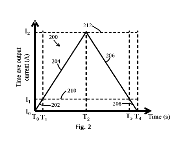
Figure 2 provides a graph that describes an illustrative dimming profile 200
often used
within solid-state lighting applications whereby a solid state light fixture
is required
35 to be switched on gradually up to a maximum allowable intensity (or
output current)
CA 03148546 2022-2-17
WO 2021/032995
PCT/GB2020/052015
22
then gradually dimmed down to an off state. The profile shows the time
averaged
output current provided through a single driver module 90 of the system
discussed in
relation to Figure 1, although it will be appreciated that this time average
current is
proportional to the intensity of the light output from the LEDs 124.
As illustrated in Figure 2, four distinct stages of dimming 202, 204, 206, 208
can be
used to achieve the dimming profile 1 in a seamless manner whilst maximising
the use
of analogue dimming at higher light intensities to promote healthy (non-
pulsed)
lighting.
The first dimming 202 stage starts at To. In the first dimming stage 202 the
output
current is increased from an initial "off" level, 10 to a threshold intensity
level II 210
at time Tt. This is referred to as a pulsed dimming Stage 1.
In a second dimming stage 204, from time T1 to time T2, the output is
increased from
II to a maximum level 12 212. The second stage 204 is referred to as analogue
dimming stage 2.
In a third dimming stage 206, from time T2 to time T3, the output is decreased
from 12
to I. The third stage 206 is referred to as analogue dimming stage 3.
In the fourth dimming stage 208, from time T3 to time Ta, the output is
decreased from
II to I. This is referred to as a pulsed dimming Stage 2.
As can be seen from Figure 2 and the above discussion, the dimming stages 202,
204,
206, 208 are either pulsed dimming 202, 208 or analogue dimming 204, 206. With
reference to Figure 2, when the output is above the threshold level 210, the
dimming
is analogue, and when the output is below the threshold 210, the dimming is
pulsed.
Therefore, the output over the full range of 10 to 12 can be considered to be
made up
of two distinct dimming phases ¨ pulsed dimming and analogue dimming. When the
desired output intensity is below the threshold 210, pulsed dimming is used,
and
above the threshold, analogue dimming is used.
CA 03148546 2022-2-17
WO 2021/032995
PCT/GB2020/052015
23
It is important to note that the output current is shown as time averaged so
that the
actual output current (and hence light fixture intensity) is comparable
irrespective of
the phase and the type of dimming used in each phase.
5 In the analogue dimming phase, the current from the driver module 90 is a
constant
current between Ii and 12, depending on the desired output intensity.
Variation of the
output intensity in the analogue dimming phase is provided by using DC dimming
such that the output module 90 is always operating within a continuous
conduction
mode.
In the analogue dimming phase, the sensor 92 detects the current at the
output. The
sensed current is used in a PID feedback control loop by the micro-controller
91, to
modify the current output from the SMPS 91 to the desired level. Therefore,
the
analogue dimming phase can be considered a closed loop control phase.
The sensor may also detect the voltage, and other variables of the power
supply and
light output to provide further control over the analogue dimming phase.
In the analogue dimming phase, the SMPS 91 in the Buck converter in the output
driver stage 90 is operating in a continuous conduction mode, where the
current
through the inductor of the converter is never 0. The analogue dimming phase
may
reduce light output by reducing various parameters of the pulsed signal from
the
SMPS. This includes the switching frequency of the pulsed signal. At
sufficiently low
dimming level, the Buck converter would transition to discontinuous operation,
which
25 is inherently unstable. However, as this transition to discontinuous
operation occurs
the system 1 switches to the pulsed dimming phase.
In the pulsed dimming phase, the output of the SMPS is switched between
periods in
continuous operation (i.e. periods in an ON state) and periods in the OFF
state. The
30 periods in the ON state include one or more pulses, whilst the periods
in the OFF state
have no output at all. The switching frequency of the SMPS is controlled so
that
during the ON state, the Buck converter is operating in continuous mode.
The pulsed dimming phase is an open control loop phase, in that it does not
make use
35 of feedback from the current sensor. Instead, the micro-controller 91
controls the
CA 03148546 2022-2-17
WO 2021/032995
PCT/GB2020/052015
24
output driver module 90 and SMPS to provide the desired averaged current level
based
on known factors of the output power signal.
Figure 3 illustrates an example of a first pulsed signal 302 for providing a
first
5 intensity level Ix in the pulsed dimming phase. This includes a number of
periods
306a-d when the SMPS 91 is in the ON state, separate by periods in the OFF
state.
Each ON state period 306 includes a number of pulses such that the Buck
converter is
operating in continuous conduction mode. The duration of the OFF state
corresponds
to at least one pulse.
Figure 3 further illustrates three examples of signals 304a-c that can provide
a second
intensity level 1,a2 which is half that of the first intensity level.
In a first example 304a, the duration of each of the ON periods is halved. In
the
15 second example 304b, the duration of the ON periods is the same as the
first example
302, but two of the ON periods are omitted. In a third example 304c, the
intensity of
the pulses in each ON period is halved. In each case, the time averaged
current over a
fixed period is equal to half that of the first intensity level h.
20 As can be seen from Figure 3, assuming the frequency of the pulses in
each signal
302, 304a-c is constant, then the intensity is halved by halving the number of
pulses.
Thus, in one embodiment, the micro-controller 91 may simply control the number
of
pulses emitted through the output driver module, for example by counting, to
control
the output to various dimming levels. No feedback from the current sensor is
required.
In the signals shown in Figure 3, the pattern of the ON periods is regular
(i.e. periods
of fixed duration spaced apart by a fixed duration OFF period). It will be
appreciated
that in other examples, the output may be a random pattern of ON and OFF
periods,
that may be repeated periodically.
Furthermore, in other embodiments, various one or more of the parameters of
the
pulses may be varied, provided continuous conduction operation is maintained
for the
ON period. For example, the switching frequency, pulse duration and amplitude
of
each pulse may be varied.
CA 03148546 2022-2-17
WO 2021/032995
PCT/GB2020/052015
In at least some embodiments, the micro-controller 91 may access look-up
tables in
order to determine the desired output signal for a particular desired current.
The
micro-controller 91 may determine a desired output level, and retrieve the
characteristics of the output signal required to achieve that intensity from
the
5 corresponding line of the lookup table. The lookup tables may be stored
in a memory
of the micro-controller 93, master controller 2, or may be accessible through
the
interface 3 or bus 24.
The dimming resolution of an illumination system 1 such as described above is
the
10 incremental increase (or decrease) in output intensity between adjacent
dimming
levels. In other words, the dimming resolution is the minimum change in
intensity
level that the system 1 may provide. A low resolution corresponds to large
steps in
output between levels, whilst a high resolution corresponds to small steps.
15 In typical dimming systems, the dimming resolution may be constant
across the entire
output intensity range. However, in the system 1 discussed above, the dimming
resolution may vary between the two dimming phases.
For example, in the analogue dimming phase, the dimming resolution may be a
first
20 resolution, and in the pulsed dimming phase, the dimming resolution may
be a second
resolution. The second resolution may be lower than the first, such that the
dimming
varies by smaller increments in the analogue dimming phase_ In other examples,
the
dimming resolution may be the same across both phases. In a further example
the
pulsed dimming may have a higher resolution than the analogue dimming phase.
It will be appreciated that although the analogue dimming phase may appear to
have a
continuously varying current, there will still be a minimum resolution defined
by the
incremental changes possible with the hardware implementing the dimming.
30 In the pulsed dimming phase, the resolution is limited by a number of
factors
including the minimum stable changes in the pulsed output characteristics, and
the
number of lines available in the look-up tables.
CA 03148546 2022-2-17
WO 2021/032995
PCT/GB2020/052015
26
Over the output range of the pulsed dimming phase Io to II, the output current
is split
into a number of evenly spaced levels, defined by the resolution. The dimming
may be
N bit, where the range is split into 2' steps.
5
The first limiting factor on the resolution of
the dimming in the pulsed dimming phase
is the size of the look-up tables. Each step of the dimming requires a
separate line in
the look-up table.
The further limiting factor on the resolution in the pulsed dimming phase is
the pulse
10
characteristics of the output pulsed signal.
For example, there may be a minimum Ton
and/or a minimum amplitude for the pulses in the signal which can be regularly
repeated in a stable manner such that all pulses are provided to the output
without
being missed. The fundamental switching frequency (f,i,,h) of the pulsed
signal may
also limit the resolution.
In one example, where dimming in the pulsed dimming phase is achieved by
varying
the number of pulses per second, the number of pulses provided at an output
level may
be given by:
[switch
R
Where:
20
P is the number of pulses per second (split
over one or more ON periods),
which determines the output
n is the output intensity level, and
R is the number of different dimming steps in the pulsed dimming range.
25
For any given single stage switch regulator
topology there is a defined minimum
output stability level at which continuous conduction mode may be maintained.
This is
determined by the various component tolerances and minimum feedback errors
associated with the switch regulator topology. Using only the analogue dimming
phase, once the desired output current drops below the minimum stability level
the
30
switch regulator becomes unstable and the
output current will fluctuate unpredictably
resulting in visible flicker to the human eye which is highly undesirable. The
threshold 210 for changing between the pulsed dimming phase and the analogue
dimming phase is thus determined based on the lower limit at which continuous
conduction mode can be maintained. The threshold may, for example, be selected
to
CA 03148546 2022-2-17
WO 2021/032995
PCT/GB2020/052015
27
be just above this limit. The threshold 210 is chosen at the minimum level at
which
the noise on the current or voltage sensor is at an acceptable level to
accurately
provide feedback for the closed loop analogue dimming phase. Therefore, the
pulsed
dimming takes over when the sensor is no longer able to provide reliable
feedback.
In at least some embodiments, an auto-correction may be applied when the
output
intensity is increased from a level below the threshold 210 to a level above
the
threshold 210. When the output is at or just below the threshold 210, but
dimming has
not switched to the analogue dimming control, the feedback from the sensor is
measured. When a command is received to increase the output, the measured
current
across the output is compared to the threshold 210. A correction is then
applied so that
the analogue dimming phase increments the output from the measured current
rather
than the expected threshold. The new threshold is also stored for future use,
rather
than the previous threshold.
In other words, the auto-correction starts measuring the feedback before the
control is
switched to the closed control loop. The measured feedback is then used in the
first
iteration of the closed control loop.
During the analogue dimming phase, the output may be modulated to transmit
data in
the light. Data to be transmitted is received and encoded in modulations of
the output
voltage. This may be sensed by a corresponding detector and decoded
accordingly.
The lighting system 1 may further include a detector (not shown) to enable
reception
of data as well as transmission.
The current for the modulation of the output may be provided by a separate
current
source or current sink, that is controllable independently of the main output
driver
module 90. The switch regulator provides the majority of the power, whilst the
current
source or current sink provides the modulation. The current source or current
sink may
be connected in parallel to the output and may provide between 5% and 0% of
the
output power.
The high frequency output signal enables the light emitting diode load(s)
connected to
the output driver module(s) to vary the intensity proportionally to variations
in the
amplitude of the load current/power. Such optical variations can be easily
picked up
CA 03148546 2022-2-17
WO 2021/032995
PCT/GB2020/052015
28
by receivers connected to or integrated with networked devices to transmit
information.
Figure 4 illustrates on example of a circuit 300a of an output driver module
90 for the
5 illumination system discussed above. In the example shown, the output
driver module
90 is in the form of a Buck converter topology.
The LED fixture 120 is connected across the output 302a,b. The sensors 304 is
provided as a current sense resistor and measures the current flowing the LED
fixture
10 120. The sensor 304 is provided on the high side of the system to allow
multiple
output driver modules to be connected to the same system and still
independently
measure the current through each LED fixture. A short circuit sense resistor
306 is
also provided in the circuit 300 that shuts down automatically the
microprocessor
signal GATE_2 when a specific voltage is reached across the sense resistor.
The
15 current sense monitor 310 provides current feedback to the
microprocessor used for
controlling the switching MOSFET 308. Fixing the ratio of the short circuit
sense
resistor 306 value and resistor R210 allows a hardware trip to occur when a
trip
current through the LED fixture 120 happens within nanoseconds and reduces any
possible LED fixture 120 damage due to overcurrent
The output driver module circuit 300 includes a switching MOSFET 308. The
MOSFET controls the power and hence voltage and/or current on the output
channels
302a,b. The MOSFET 308 is in turn controlled by a micro-controller. During the
pulsed dimming phase, the micro-controller (not shown) controls operation of
the
25 MOSFET 308 via signal GATE_2 to open and close the channel through the
MOSFET
308, and thus provide a pulsed output at the output channel 302a,b.
In the example discussed above, the output range of the system 1 is provided
by two
different dimming phases - a pulsed dimming phase and an analogue dimming
phase.
30 It will be appreciated that this is by way of example only. Any number
of additional
dimming phases may be provided in addition to the pulsed dimming and analogue
dimming.
The system illustrated in Figure 1 is given by way of example only. It will be
35 appreciated that the various functions discussed may be omitted or may
be provided in
CA 03148546 2022-2-17
WO 2021/032995
PCT/GB2020/052015
29
any suitable way without discrete modules. The discrete modules are disclosed
for
illustrative purposed only.
It will be appreciated that the profile of Figure 2 is given by way of example
only
5 also, to illustrate certain embodiments of the invention. The true
dimming profile of a
system may include various points where the output is held constant for a
period of
time. The output need never by increased to the maximum, and may be switched
on
and off at any level, rather than increasing and decreasing from a minimum.
10 In the examples discussed above, one or more electronic parameters of
the system (for
example current, voltage, or power) are measured to control the dimming cycle.
It will
be appreciated that other parameters may be detected and used in the control
of the
dimming. For example, the system may also include sensors to detect one or
more of:
ambient lighting levels (in lux), colour sensors to detect the colour output
from the
15 LED fixtures 120, and occupancy (for example a passive infrared detector
or
microwave detector)
By detecting ambient lighting levels, the dimming output can be controlled so
that the
correct lighting can be achieved (for example in high ambient lighting levels,
light
20 output from the LEDs 124 can be reduced in low ambient lighting levels,
light output
from the LEDs 124 can be increased. By detecting colour, the output from
different
LEDs fixtures can be varied to achieve the desired lighting effect. By
detecting
occupancy, the dimming can be controlled so the lighting fixture 124 is only
powered
when needed. For example, if no occupancy is detected within a threshold time
(for
25 example 30 seconds), the light output can be reduced.
As with the dimming discussed above, these functions are now being built
directly
into the LED drivers, rather than using an external controller. Doing this
offers a
lower cost and localised/distributed control.
In variants of the current invention the time averaged output current could be
derived
for a constant voltage based
output switching module.
CA 03148546 2022-2-17