Note: Descriptions are shown in the official language in which they were submitted.
CA 03150269 2022-02-07
WO 2021/030371 PCT/US2020/045807
1
Step-Wise Power Transformation
CROSS-REFERENCE TO RELATED APPLICATION
This application claims priority of Provisional Patent Application 62/885,275
filed on August 11,
2019, the entire contents of which are incorporated herein by reference for
all purposes.
FIELD
This disclosure pertains to transformation of electric power from one voltage
to another in short
incremental steps by means of capacitive energy exchanges
BACKGROUND
Early in the history of electric power systems, the introduction of a
magnetically based
transformer forced early direct-current systems to give way to alternating
current systems in
which generator output voltage could be converted to higher voltages, and
proportionately lower
currents, for long distance delivery. Today's power systems transform
generated power to
transmission networks operating at hundreds of kilovolts and spanning hundreds
of miles. While
magnetically-based transformers serve principally to link power transmission
and distribution
systems of differing voltage levels, specially-built transformers can also
shift electrical phase
angle from one high voltage bus to another, thereby forcing an increase or
decrease in power
transfer between them.
DESCRIPTION OF PRIOR ART
Transformer technology advanced very quickly over the first decades of power
grid evolution.
Transformers linking differing power delivery voltage levels consist of large
cores of special-
purpose laminated steel, around which are windings of insulated copper wire ¨
all immersed in a
special insulating oil. While today's magnetically-based transformers are
efficient and reliable,
their long delivery lead time often requires that a spare transformer be
readily available on site.
Furthermore, they are based on a very mature technology with little promise of
further advances.
Their insulating oil is toxic, their cost increases year-by-year, and their
technology base is quite
mature.
CA 03150269 2022-02-07
WO 2021/030371 PCT/US2020/045807
2
Though AC was universally adopted in the 1920s, a first special-purpose high
voltage DC
transmission link was introduced in 1954, wherein AC power was magnetically
transformed to a
high AC voltage then converted to high voltage DC for delivery to a remote
location where it
was re-converted to AC for linking to the local AC network. DC had the
advantage of low-cost
towers, the electrical capability of very long-distance transfer, and the
capability of controlled
power flow.
The mercury arc valves used in the earliest AC-to-DC converter stations were
soon displaced by
solid state valves having lower cost and greater reliability. As the use of DC
links increased,
valve design improved and a new method of commutation was introduced; one
capable of
generating reactive power rather than being required to consume it. High
Voltage DC (HVDC)
projects now abound throughout the world for special purpose, point-to-point
transmission tasks
but, for lack of suitably priced high voltage DC circuit breakers compared to
high voltage AC
circuit breakers, are not cost effective for forming networks similar to those
characterizing high
voltage AC systems.
Meanwhile, the realization of global climate change triggered a major shift in
generation sources,
principally to wind and solar sites. This shift will change the role of
today's transmission systems
by imposing geographically broad weather-related irregularities in energy
production capability.
The solution to that shift was recognized to be construction of a
geographically broad HVDC
"supergrid," overlaying today's AC transmission system. But it was also
acknowledged that in
order for HVDC to operate as a network, rather than a point-to-point
expedient, the DC
equivalent of the AC transformer had to be invented. Thus, began multiple
investigations on how
to transform between two high voltage DC systems.
One DC transformer (DCT), consisting of a column of capacitors, is disclosed
in US Patent
Number 10,284,080 B2, the disclosure of which is incorporated herein by
reference in its
entirety.
SUMMARY
This disclosure achieves exchange of energy between multiple electrical nodes
by a high-speed,
repeating three step process, the first step being a resonant half-cycle
exchange of energy
between a first voltage node and a column of series-connected capacitors, the
second being
CA 03150269 2022-02-07
WO 2021/030371 PCT/US2020/045807
3
electrical reconfiguration of capacitors within the series-connected column,
and the third being a
resonant half-cycle exchange of energy between the reconfigured column and one
or more
secondary nodes.
The disclosure will serve to replace existing magnetically-based AC
transformers, offering the
advantages of (1) internal redundancy sufficient to obviate the need for the
spare transformer
normally supplied with magnetic transformation, (2) absence of toxic
insulating oil, (3) ease of
manufacture, being modular in construction, (4) inherent phase shifting
capability, and (5) the
ability to convert between primary and secondary nodes differing in frequency
and/or wave-
shape.
The foregoing is accomplished through use of a controller which translates
prescribed
transformation functions into the selection of both the active number and
connection polarity of
multiple series-connected capacitive modules which, in the aggregate, (1)
resonantly receive
electrical charge from a primary node (2) are electrically reconfigured and
(3) deliver electrical
charge to one or more secondary nodes.
All examples and features mentioned below can be combined in any technically
possible way.
In one aspect, a computer program product has a non-transitory computer-
readable medium
including computer program logic encoded thereon that, when performed on a
system for
transforming the voltage of AC electrical energy between multiple electrical
nodes, causes
energy exchange between the multiple electrical nodes in a series of discrete,
short increments of
time.
Some examples include one of the above and/or below features, or any
combination thereof In
some examples energy transformation is achieved by resonant charge exchange
between a first
electrical node, a capacitor or series-connected column of capacitors, and a
second electrical
node, and the computer program product causes the system to repetitively
conduct a primary
charge exchange by resonantly exchanging energy between the capacitor or the
series-connected
column of capacitors and the first node, and then electrically isolate the
capacitor or the series-
connected column of capacitors, during the electrical isolation electrically
reconfigure the series-
connected column of capacitors, and then conduct a secondary charge exchange
by resonantly
exchanging energy between the capacitor or the reconfigured series-connected
column of
CA 03150269 2022-02-07
WO 2021/030371 PCT/US2020/045807
4
capacitors and the second node. In an example the computer program product
further causes the
system to determine the manner of capacitor reconfiguration during the
interval between primary
and secondary charge exchanges. In an example the computer program product
further causes the
system to leave all of the capacitors of the series-connected column of
capacitors with equal
charge following charge exchange with the secondary node.
Some examples include one of the above and/or below features, or any
combination thereof In
an example the capacitor or series-connected column of capacitors is sized to
allow the
instantaneous input voltage profile and output voltage profile to differ by
its temporary storage of
energy. In an example the system further comprises a smoothing capacitor
electrically connected
between each node and ground, to smooth both input and output waveforms. In an
example the
smoothing capacitors also participate in the resonant energy exchange for the
input and output
waveforms. In an example multiple, parallel, series-connected columns of
capacitors are
controlled to accomplish resonant energy exchange equally offset in time from
each other, to
produce smoother input and output voltage profiles.
Some examples include one of the above and/or below features, or any
combination thereof In
an example the series-connected column of capacitors is divided into multiple
unequal sections
such that, after all sections are charged in series by one node, one or more
sections are then
reconfigured in voltage opposition to the other sections before connection to
another node, to
produce a secondary voltage equal to the difference in two section voltages.
In an example the
series-connected column of capacitors is divided into multiple series-
connected sections such
that the sections can be charged from a first node in series, after which
their series connection
can be configured to serve one secondary node and their intermediate
connection can be
configured to serve another secondary node. In an example the computer program
product
further causes the system to connect a capacitor to affect a resonant energy
exchange with a first
node, then disconnected and resonantly connected to a larger capacitor,
leaving the larger
capacitor and the node to which it is connected with a voltage lower than the
voltage of the first
node.
In another aspect a system for transforming the voltage of AC electrical
energy by resonant
charge exchange between a first node and a second node includes a capacitor or
series-connected
CA 03150269 2022-02-07
WO 2021/030371 PCT/US2020/045807
column of capacitors and a controller that is configured to cause the system
to repetitively
conduct a primary charge exchange by resonantly exchanging energy between the
capacitor or
the series-connected column of capacitors and the first node and then
electrically isolate the
capacitor or the series-connected column of capacitors, during the electrical
isolation electrically
reconfigure the series-connected column of capacitors, and then conduct a
secondary charge
exchange by resonantly exchanging energy between the capacitor or the
reconfigured series-
connected column of capacitors and the second node.
Some examples include one of the above and/or below features, or any
combination thereof In
an example the controller further causes the system to determine the manner of
capacitor
reconfiguration during the interval between primary and secondary charge
exchanges. In an
example the controller further causes the system to leave all of the
capacitors of the series-
connected column of capacitors with equal charge following charge exchange
with the secondary
node. In an example the capacitor or series-connected column of capacitors is
sized to allow the
instantaneous input voltage profile and output voltage profile to differ by
its temporary storage of
energy.
Some examples include one of the above and/or below features, or any
combination thereof In
an example the system further comprises a smoothing capacitor electrically
connected between
each node and ground, to smooth both input and output waveforms. In an example
the smoothing
capacitors also participate in the resonant energy exchange for the input and
output waveforms.
In an example the system comprises multiple, parallel, series-connected
columns of capacitors
that are controlled to accomplish resonant energy exchange equally offset in
time from each
other, to produce smoother input and output voltage profiles.
Some examples include one of the above and/or below features, or any
combination thereof In
an example the series-connected column of capacitors is divided into multiple
unequal sections
such that, after all sections are charged in series by one node, one or more
sections are then
reconfigured in voltage opposition to the other sections before connection to
another node, to
produce a secondary voltage equal to the difference in two section voltages.
In an example the
series-connected column of capacitors is divided into multiple series-
connected sections such
that the sections can be charged from a first node in series, after which
their series connection
CA 03150269 2022-02-07
WO 2021/030371 PCT/US2020/045807
6
can be configured to serve one secondary node and their intermediate
connection can be
configured to serve another secondary node. In an example the controller
further causes the
system to connect a capacitor to affect a resonant energy exchange with a
first node, then
disconnected and resonantly connected to a larger capacitor, leaving the
larger capacitor and the
node to which it is connected with a voltage lower than the voltage of the
first node.
BRIEF DESCRIPTION OF THE DRAWINGS
Figure 1 illustrates a prior art "half bridge" with switches adjusted to
electrically insert its
capacitor into a series of capacitors.
Figure 2 illustrates a prior art "half bridge" with switches adjusted to
remove its capacitor from a
series of capacitors and bypass it in that series.
Figure 3 illustrates a prior art "full bridge" with switches adjusted to
insert a capacitor into a
series chain of capacitors.
Figure 4 illustrates a prior art "full bridge" with switches adjusted to
remove a capacitor from a
series chain of capacitors and electrically bypass it in that series.
Figure 5 illustrates a prior art "full bridge" with switches adjusted to
insert a capacitor into a
series chain of capacitors with its connection polarity reversed.
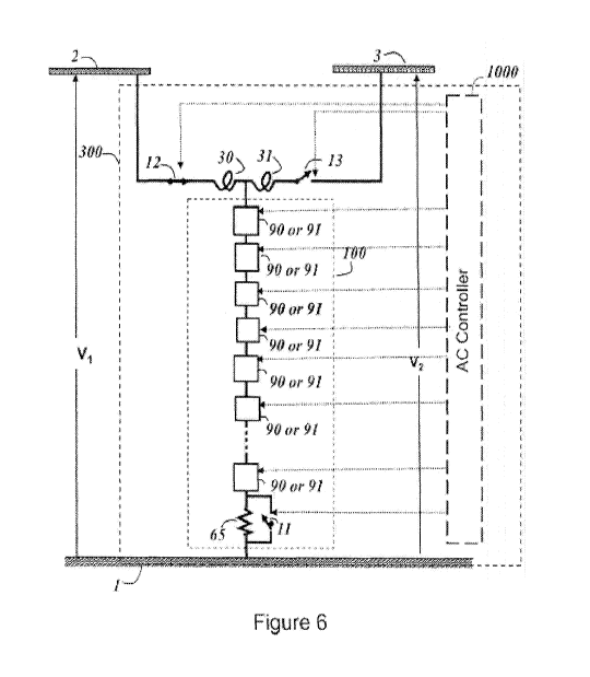
Figure 6 illustrates a series-connected column of capacitors connected to
resonantly exchange
charge with the first of two electrical nodes
Figure 7 illustrates the series-connected column of capacitors of figure 6
after disconnection
from the first of two electrical nodes, reconfiguration of capacitors
comprising the column of
capacitors, and connected for resonant exchange of charge with a second
electrical node.
Figure 8 shows the wave form of both primary and secondary currents resulting
from alternate
exchange of charge of a capacitive column first to one AC electrical node and
then another AC
electrical node.
Figure 9 shows, for a primary connection, a means of partially smoothing the
output of the
single-column embodiment of figure 7 and participate in the resonant charging
and discharging.
CA 03150269 2022-02-07
WO 2021/030371 PCT/US2020/045807
7
Figure 10 shows, for a secondary connection, a means of partially smoothing
the output of the
single-column embodiment of figure 7 and participate in the resonant charging
and discharging.
Figure 11 shows an example waveform of input or output resulting from the
smoothing effect of
the smoothing capacitors used in figures 9 and 10.
Figure 12 shows an example use of multiple capacitive columns in parallel,
operation of each
offset from each other by an equal time increment.
Figure 13 shows an example waveform resulting from the use of three columns,
each equally
offset in timing from the other.
Figure 14 shows a primary connection of a capacitive column split into two
segments, enabling
the two segments to be made to oppose one another during secondary connection
thus producing
a difference voltage.
Figure 15 shows a secondary connection of a capacitive column split into two
segments,
enabling the two segments to be made to oppose one another during secondary
connection thus
producing a difference voltage.
Figure 16 shows the configuration of figure 14 except with smoothing
capacitors at one or more
terminals to smooth input and/or output voltage and participate in the
resonant charging and
discharging.
Figure 17 shows the configuration of figure 15 upon connection to the
transformer's secondary
node except with smoothing capacitors at one or more terminals to smooth input
and/or output
voltage and participate in the resonant charging and discharging.
Figure 18 shows a primary connection for a simple configuration for a large
stepdown ratio
based on the relative size of the capacitors so that during a secondary
connect the secondary is a
lower voltage.
Figure 19 shows a secondary connection for a simple configuration for a large
stepdown ratio
based on the relative size of the capacitors with the lower voltage connected
to the secondary
connection.
CA 03150269 2022-02-07
WO 2021/030371 PCT/US2020/045807
8
Figure 20 shows the primary connection of a capacitive column divided into two
sections to
allow polarity reversal of one of those sections during secondary connect,
thus supplying the
secondary with a difference voltage
Figure 21 shows the secondary connections of a capacitive column divided into
two sections to
allow polarity reversal of one section during secondary connection, thus
supplying the secondary
with a difference voltage.
Figure 22 shows the primary connection of the configuration of figure 20 with
smoothing
capacitors added to provide a smoother output wave form and participate in the
resonant
charging and discharging.
Figure 23 shows the secondary connections of the configuration of figure 21
with smoothing
capacitors added to provide a smoother output wave form and participate in the
resonant
charging and discharging.
EMBODIMENTS
To simplify explanation of the embodiments cited herein, commonly used power
electronic
switching devices such as thyristors, insulated gate bipolar transistors
(IGBTs) and diodes that
may be silicon, silicon carbide or other semiconductor-based switching devices
are all
represented herein by simple switch symbols, their function being made clear
from the context of
the figures presented. The more general identification of "nodes" will, in
higher voltage power
applications, correspond to "busses" in such applications. Also, to simplify
explanations, the
same numbers are sometimes used in multiple drawings to refer to the same
element, and such
elements are not necessarily discussed in conjunction with each drawing in
which they are
present.
Embodiments cited herein are based on electrical charge transfers between
electrical nodes by
means of intermediate transfer into and out of a series-connected column of
capacitors, each such
intermediate transfer being made to have a sinusoidal wave shape by placing an
inductance in
series with the switching device affecting such transfer. This sinusoidal wave
shape with its
resulting current zero facilitates the interruption at that point in time by
power electronic
switching devices, e.g. thyristors or solid-state bidirectional switches,
leaving the capacitor(s)
CA 03150269 2022-02-07
WO 2021/030371 PCT/US2020/045807
9
with either an increase or decrease in charge and a corresponding higher or
lower voltage. The
principles of such resonant transfers are well known to those versed in the
art.
Usefulness in application of the above principles is enhanced in the
embodiments cited herein by
providing a means, as shown in figure I, to electrically bypass individual
capacitors 80 e.g., by
inserting each capacitor 80 within a half-bridge 90, thus allowing its
insertion into a series
column by closing of switch 72 and opening of switch 73 or electrically
bypasses the capacitor
80 by opening switch 72 and closing switch 73 as shown in figure 2.
Alternatively, a full bridge 91 as shown in figure 3 allows either (1)
inserting the capacitor 80
into the column in its original orientation by closing switches 74 and 77
while opening switches
75 and 76, (2) isolating and by-passing the capacitor 80 by closing switches
74 and 76 while
opening switches 75 and 77 as shown in figure 4, or (3) inserting the
capacitor 80 into the
column 100 with its electrical polarity reversed by closing switches 75 and 76
and opening
switches 74 and 77 as shown in figure 5.
In both figures and text describing various embodiments of this disclosure,
various nodes are, for
ease of understanding, referred to as "primary nodes" or "secondary nodes." It
will be apparent
to those versed in the art that all embodiments are bilateral and will allow
nodes identified as
secondary nodes to function as primary nodes and those identified as primary
nodes to serve as
secondary nodes.
Figure 6 shows the first embodiment of the present step-wise power
transformation system 300,
capable of transforming energy from one voltage to another voltage by means of
a series of short
resonant charge exchanges, each of which may be at a progressively higher or
lower voltage, e.g.
describing a sinusoidal profile wherein, for each such exchange, a column 100
of half-bridge or
full-bridge capacitive modules 90 or 91 is first made to exchange charge
resonantly with the
primary node 2 at its instantaneous voltage and polarity by closure of switch
12 in figure 6, that
resonant exchange being interrupted at its first current zero through node 1
which is represented
as ground in this and subsequent embodiments. During that connection, the
resonant frequency
of the half-sine wave exchange is determined by a reactor 30 and the effective
capacitance of the
column 100, that capacitance resulting from series connection of most or all
capacitive modules
90 or 91 within the column 100 and any component such as a filter (not shown
in this figure) or
CA 03150269 2022-02-07
WO 2021/030371 PCT/US2020/045807
capacitor (not shown in this figure) connected between node 2 and ground.
After such charge
exchange with node 2, switch 12 is opened and the column 100 momentarily
isolated, during
which isolation, capacitors 80 within various modules 90 or 91 can be
individually isolated and
bypassed, left to be included in the column 100 at their original polarity, or
removed and then re-
inserted into the series column 100 with their polarity reversed. The new
voltage of column 100
then establishes the basis for second resonant charge exchange, again
interrupted at its first
current zero, between the reconfigured column 100 and the secondary node 3,
initiated by
closure of switch 13 as illustrated in figure 7. In the latter case the
resonant frequency of the
charge exchange is determined by the reactance of a second reactor 31 and the
effective
capacitive of the reconfigured capacitive column 100 and any component such as
a filter(not
shown in this figure) or capacitor (not shown in this figure) connected to
node 3 and ground. An
ongoing repetition of the foregoing three-step switching cycle may be made
either with the same
secondary column 100 reconfiguration from one cycle to the next, thus causing
the secondary
node 3 voltage profile to track the voltage profile of the primary node 2 or
by changing the
capacitor column 100 reconfiguration from one discharge cycle to the next,
causing the
secondary node 3 voltage profile to differ from the primary node 2 voltage
profile. It will be
apparent that any difference between input and output voltage profile will
imply energy storage
within the capacitive column 100.
Switching logic, supplied by an AC controller 1000 in figures 6 and 7,
controls the opening and
closing timing of switches 11, 12, and 13 in those figures as well as the
logic for any or all of (1)
electrically bypassing certain capacitors 80 within modules 90 or 91, (2)
insertion of those
modules 90 or 91 in the series connected column 100 with capacitors 80
retaining their original
polarity, (3) in the case of modules comprise of full bridges 91, reversal of
electrical polarity of
the capacitor's 80 connection within the module 91 prior to re-inserting it
into the column 100,
or (4) opening and closing any switches in the system. That controller 1000 is
implicitly included
in and exhibits control in the manners as discussed relative to all
embodiments later discussed
but is omitted from subsequent drawings for the sake of simplicity of
illustration.
If the total capacitive column 100 in figures 6 and 7 is comprised of n
capacitive modules 90 or
91, m of which are electrically bypassed in the interval between the charge
exchange between
CA 03150269 2022-02-07
WO 2021/030371 PCT/US2020/045807
11
column 100 and node 2, and its exchange with node 3, the voltage ratio V1N2 in
those figures
will be n/(n-m).
Absent any corrective measure, any one such charge exchange of the column 100
with the
secondary node 3 in figure 7, would leave m of the capacitive modules 90 or 91
with a charge
level differing from that of the n-m modules that were active in the charge
exchange with that
secondary node 3. This charge disparity can be corrected if, during connection
of the
reconfigured column 100 to the secondary node 3, participation in the n-m
module group is
shared through internal switching so that all n capacitive modules 90 or 91
within the column
100, are left with equal charge in a process called "sorting" that is commonly
used in high
voltage DC to AC converter applications. It will be clear from the foregoing
that the embodiment
shown in figures 6 and 7 can, by sorting, also cause the sum of individual n
module voltages
following charge exchange with the primary node 2 to be greater than the
voltage of that node 2
by having available within the column 100 a number of modules 90 or 91, the
sum of whose
voltage ratings exceeds the maximum voltage Vi on the primary node 2 and by
allowing each
such module 90 or 91 to share, in time, the number of modules 90 or 91 forming
a voltage
corresponding to the voltage of the primary node 2. It will be apparent that
the designation of
"primary" and "secondary" nodes in the first and subsequent embodiments is
somewhat arbitrary
in that any of the secondary nodes cited in this and subsequent embodiments
could also serve as
a primary node in the charge exchange as could any primary node serve as a
secondary. Resistor
65 in figures 6 and 7 is temporarily inserted into the column 100 upon initial
energization of this
and subsequent embodiments with all capacitive modules 90 or 91 in electrical
series in order to
bring the column 100, on initial energization, up to the voltage Vi, after
which that resistor 65 is
bypassed by closure of switch 11 and kept isolated for normal operation. For
simplicity, this
resistor 65 and its bypass switch 11 are omitted in subsequent figures.
Both primary and secondary current wave forms resulting from the example
single-column
transformation embodiment shown in figures 6 and 7 will be in the form of half
sine wave pulses
as shown in figure 8. The pulse duration can be but need not be at the input
duration (e.g., 120
cycles per second) or otherwise. For example, each such resonant pulse can be
controlled to have
a duration during connection with the primary node 2 determined by the reactor
30 and the
effective capacitance of all modules 90 or 91 in series and so is
controllable. The duration of the
CA 03150269 2022-02-07
WO 2021/030371 PCT/US2020/045807
12
subsequent half-sine wave current pulse resulting from the resonant connection
of the capacitive
column 100 to the secondary node 3 will be determined by the secondary reactor
31 and the
capacitance of the capacitive column 100 as modified by reconfiguration
between charge
exchanges and so is also controllable. Accommodation of the intermittent pulse
waveform
resulting from such resonant exchanges, separated in both primary and
secondary wave form by
a zero-current interval during the period of charge exchange with the
alternative node 2 or 3, will
depend on the context in which this embodiment is used. Its acceptability can
be enhanced by a
second embodiment which employs smoothing capacitors 87 and 88 at each
terminal or node, as
shown in figure 9 in its primary connection and figure 10 in its secondary
connection, the result
of either being a waveform which, depending on the external resistive load on
node 3 (not
shown) would decay between cycles as shown in figure 11 as well as participate
in the resonant
energy exchanges.
A third embodiment, which uses multiple, paralleled capacitive columns 100 of
the first
embodiment, the input and output waveforms of which are equally offset from
one another in
time, is shown for a three-column example in figure 12, the resulting input
and output voltage
waveforms of which are shown in figure 13.
The foregoing embodiments which achieve transformation through an ongoing
series of very
short energy pulses rather than a continuous process, can adjust the
transformation voltage ratio
from one very short energy exchange cycle to the next. As such, these and
subsequent
embodiments are capable of transforming between a primary voltage waveform
that differs from
the secondary waveform providing that (a) the average energy per unit time
represented by the
two waveforms is equal and (b) the capacitive column is capable of storing
differences between
momentary energy input and energy output.
It will be apparent to those versed in the art, that the foregoing embodiments
will be increasingly
difficult to apply as the ratio between primary and secondary voltage,
V1/V2becomes very high,
as is the case in transformers stepping down to utilization voltages.
A fourth embodiment, illustrated in figure 14 for its primary connection and
figure 15 for its
secondary connection, achieves high ratio transformation by using the
controller to segment the
capacitive column 100 in figure 9 into two segments 105, 106; one with n
active modules and the
CA 03150269 2022-02-07
WO 2021/030371 PCT/US2020/045807
13
other with m active modules, at least one of those segments having its
capacitors embedded in
full bridge modules and thus capable of polarity reversal during the interval
between connection
to nodes 2 and 4. Thus, by charging the two column segments 105, 106 in
figures 14 and 15 in
series and reversing only the segment with m modules prior to connection to
the secondary node
4, a transformation ratio of (m+n)/(m-n) is achieved; a configuration well
adopted to high ratios
of primary to secondary voltage.
A fifth embodiment, illustrated in its primary connection in figure 16 and its
secondary
connection in figure 17, consists of augmenting the fourth embodiment by
adding smoothing
capacitor 87 to the primary node and/or smoothing capacitor 88 to the
secondary node 4 to
smooth the current waveform in either or both as well as participate in the
resonant exchanges.
A sixth embodiment illustrated in figure 18 for its primary connection and
figure 19 for its
secondary connection achieves a high ratio transformation as presented in the
fourth embodiment
but with energy flow in one direction for a large voltage stepdown ratio from
primary node 2 to
secondary node 3 Capacitor 84 is resonantly charged through reactor 30 from
node 2 with
switch 12 closed and switch 13 open as shown in Figure 18 Low voltage
capacitor 85 is
resonantly charged from capacitor 84 through reactor 31 in Figure 19 with
switch 12 open and
switch 13 closed. The high voltage ratio from the primary connection 2 down to
the secondary
connection 3 is achieved by having a very large capacitance for capacitor 85
compared with the
much smaller capacitance value of capacitor 84. This configuration of voltage
transformer has
the disadvantage compared with the fifth embodiment of unidirectional energy
flow only from
the high voltage primary terminal to the low voltage secondary terminal but
with the advantage
of a simpler configuration compared with the fifth embodiment while still
applying resonant
charging and discharging
A seventh embodiment, illustrated in its primary connection in figure 20 and
its secondary
connection in figure 21, consists of establishing multiple secondary nodes 4,
5, having voltages,
Vy and Vz for the double secondary configuration illustrated in that figure.
While variation in the
loads on nodes 4 and 5 during the secondary charge exchanges may cause the
post-discharge
ratio of voltages on the two column sections 105, 106 to differ from their
nominal voltage ratio,
that nominal ratio can be restored during the subsequent charge exchanges with
node 2 by
CA 03150269 2022-02-07
WO 2021/030371 PCT/US2020/045807
14
controlling the selective bypassing of individual capacitive modules during
connection to that
node as within the example configurations shown in figures 16 and 17.
It is also apparent, with reference to figures 20 and 21, that adjustments to
the susceptance within
the two column sections shown 105, 106 in order to maintain voltages Vz and Vy
at their nominal
value while the external load on these nodes 4, 5 vary, will also result in
changes to the
frequency of the resonant exchange of energy from the capacitive column 100 to
each of these
nodes 4, 5 and therefor disparities in the time of opening of the associated
secondary switches
14, 15. This disparity will delay the overall period of the switching cycle to
the period of the
slowest secondary pulse width.
An eighth embodiment illustrated in figure 22 in its connection to the primary
node 2 and in
figure 23 in its subsequent connection to the secondary nodes 4, 5, aids in
smoothing the current
waveform of the seventh embodiment by means of a shunt capacitor 86 on the
primary node 2
and/or addition of shunt capacitors 87, 88 on each of the secondary nodes 4
and 5. As these
capacitors 88 and 87 participate in the resonant exchanges, they are sized to
be dominant in
defining the resonant frequency of the secondary circuits for nodes 4 and 5
correspondingly
Elements of figures are shown and described as discrete elements in a block
diagram. These may
be implemented as one or more of analog circuitry or digital circuitry.
Alternatively, or
additionally, they may be implemented with one or more microprocessors
executing software
instructions. The software instructions can include digital signal processing
instructions.
Operations may be performed by analog circuitry or by a microprocessor
executing software that
performs the equivalent of the analog operation. Signal lines may be
implemented as discrete
analog or digital signal lines, as a discrete digital signal line with
appropriate signal processing
that is able to process separate signals, and/or as elements of a wireless
communication system.
When processes are represented or implied in the block diagram, the steps may
be performed by
one element or a plurality of elements. The steps may be performed together or
at different times.
The elements that perform the activities may be physically the same or
proximate one another, or
may be physically separate. One element may perform the actions of more than
one block.
Examples of the systems and methods described herein comprise computer
components and
computer-implemented steps that will be apparent to those skilled in the art.
For example, it
CA 03150269 2022-02-07
WO 2021/030371
PCT/US2020/045807
should be understood by one of skill in the art that the computer-implemented
steps may be
stored as computer-executable instructions on a computer-readable medium such
as, for
example, hard disks, optical disks, Flash ROMS, nonvolatile ROM, and RAM.
Furthermore, it
should be understood by one of skill in the art that the computer-executable
instructions may be
executed on a variety of processors such as, for example, microprocessors,
digital signal
processors, gate arrays, etc. For ease of exposition, not every step or
element of the systems and
methods described above is described herein as part of a computer system, but
those skilled in
the art will recognize that each step or element may have a corresponding
computer system or
software component. Such computer system and/or software components are
therefore enabled
by describing their corresponding steps or elements (that is, their
functionality), and are within
the scope of the disclosure.
A number of implementations have been described. Nevertheless, it will be
understood that
additional modifications may be made without departing from the scope of the
inventive
concepts described herein, and, accordingly, other examples are within the
scope of the
following claims.