Note: Descriptions are shown in the official language in which they were submitted.
WO 2021/048560
PCT/GB2020/052193
1
Single Photon Sources
Field of the Invention
The present invention relates to single photon sources (SPSs), and in
particular to
5 optically triggered single photon sources. It has application in a number
of fields, such
as quantum cryptography, optical quantum computation, optical quantum
metrology,
and optical quantum simulators.
Background
10 Single-photon sources (SPSs), in general, can be characterised as
emitting a single
photon at each trigger event, providing deterministic generation, i.e. every
trigger
event generates a photon, producing no entanglement between photons by default
but
multiple emitters can be used to generate entanglement. SPSs can be triggered
optically or electrically.
A number of methods of making SPSs have been suggested. Quantum dot (QD)-based
devices have emerged as a primary source of high-quality indistinguishable
SPSs
suitable for quantum applications. QDs exhibit discrete exciton energy levels.
When
an exciton decays it emits a single photon. In these systems, QDs are placed
inside
20 photonic structures, such as photonic crystal (PhC) waveguides, to
extract SPS
emission (see, e.g. P. Lodahl, "Quantum-dot based photonic quantum networks,"
Quantum Sci, Technol., vol, 3, no. 1, p. 13001, 2018, and 6B2378319), Optical
resonators, often implemented as photonic crystal cavities (PhCC), can also be
incorporated, for example in the waveguides, to impact emission properties.
One
25 option is to use the so-called Purcell enhancement of a cavity to reduce
the QD
exciton lifetime, increasing both the single photon emission rate and the
resilience to
dephasing processes such as charge noise that can compromise
indistinguishability of
the photons. Proof-of-principle demonstrations of this system (QD in a PhCC
utilising
Purcell enhancement) as suitable for generation of indistinguishable single
photons at
30 very high rates have been made.
One of the key challenges for making practical SPSs is ensuring that they are
deterministic and that each photon is emitted within the smallest possible
time
uncertainty relative to the trigger. Resonant optical triggering schemes (i.e.
with laser
35 light of the same energy as the single-photon emission) are superior to
electrical or
CA 03150885 2022-3-10
WO 2021/048560
PCT/GB2020/052193
2
off-resonant optical triggering as they avoid introducing intermediate
electron/hole
states that reduce determinism and increase time uncertainty. However, the
major
problem of resonant optical excitation schemes is the need to separate the
driving
laser from the single photon emission.
Previously it has been suggested (see e.g. "High Purcell Factor Generation of
Undistinguishable On-Chip Single Photons" F. Liu et al., Nature
Nanotechnology, vol.
13, p835-840 2018; and "Polarized Indistinguishable Single Photons from a
Quantum
Dot in an Elliptical Micropillar" Yu-Ming He et al.,
arXiv:1809. 10992
[physics.optics]) to use asymmetric 2D-cavities to couple orthogonally
polarised
photonic cavity modes to a QD; one mode to the QD exciton transition and the
other
to the (slightly de-tuned) laser energy, therefore building a polarisation-
filtering
scheme. In the systems described in both of these papers the cavity modes are
aligned
with the crystal axes and hence with the long and short axes of the elliptical
micropillar. "Polarized Quantum Dot Cavity-QED and Single Photons" H.J.
Snijders
et al., arXiv:1811.10571[physics.optics] describes a system which allows the
angle
between the cavity and the QD states to be changed.
Summary of the Invention
The present invention further provides, according to a first aspect, a photon
source
comprising: a photon emitter, an excitation waveguide arranged to direct
excitation
photons having a first polarisation direction into the photon emitter, and a
collection
waveguide arranged to collect photons having a second polarization direction
from the
photon emitter, wherein the first polarisation direction is coupled to a first
exciton
state of the photon emitter and the second polarisation direction is non-
parallel to the
first polarisation direction and is coupled to a second exciton state of the
photon
emitter, and the first and second exciton states have substantially equal
energies.
The first polarization direction and the second polarization direction may be
substantially mutually perpendicular.
The photon emitter may comprise a quantum dot. The quantum dot may be circular
or
oval. The quantum dot may have a short axis, and a long axis which is
perpendicular
to the short axis.
CA 03150885 2022-3-10
WO 2021/048560
PCT/GB2020/052193
3
The excitation waveguide may be arranged to direct photons into the photon
emitter in
an excitation direction and the collection waveguide may be arranged to
collect
photons emitted from the photon source in a collection direction.
5 The excitation direction may be offset from the long axis by an
excitation direction
offset angle. The collection direction may be offset from the long axis by a
collection
direction offset angle. The excitation direction offset angle may be equal to
the
collection direction offset angle. The excitation direction offset angle and
the
collection direction offset angle may each be about 45 .
The photon emitter may be a colour centre in diamond, for example a nitrogen-
vacancy centre or a silicon-vacancy centre, or the photon emitter may be a
defect in a
2D material.
15 The photon source may further comprise a source of magnetic field
arranged to apply
a magnetic field to the photon emitter which is perpendicular to both the
first and
second polarisation directions.
The present invention provides, according to a first aspect, a photon source
20 comprising: a quantum dot having a long axis, and a short axis
perpendicular to the
long axis, an excitation waveguide arranged to direct photons into the quantum
dot in
an excitation direction, and a collection waveguide arranged to collect
photons
emitted from the quantum dot in a collection direction, wherein the excitation
direction and the collection direction are non-parallel to each other and the
diameter
25 of the quantum dot in the collection direction is substantially equal to
the diameter of
the quantum dot in the excitation direction.
The excitation direction and the collection direction may be substantially
mutually
perpendicular.
The photon source may further comprise a source of magnetic field arranged to
apply
a magnetic field to the photon emitter which is perpendicular to both the
excitation
direction and the collection direction.
CA 03150885 2022-3-10
WO 2021/048560
PCT/GB2020/052193
4
The waveguides in either aspect of the invention may be arranged at least
partly to
form at least one reflector thereby to form a photonic crystal cavity. The
photonic
crystal cavity may comprise just one reflector, or it may comprise two
reflectors, one
on each side of the cavity, with one of the reflectors being more strongly
reflecting
5 than the other. In this way the photonic crystal cavity may be asymmetric
so as to
induce Purcell enhancement of the emission of photons into the collection
waveguide.
The reflector may comprise a Bragg reflector.
Brief Description of the Drawings
10 Figures la and lb show the exciton energies of exciton states
associated with
orthogonal excitation polarization directions aligned with the
crystallographic
axes of an asymmetric quantum dot;
Figures 2a and 2b show the exciton energies of exciton states associated with
15 orthogonal excitation polarization directions at 450 to the
crystallographic
axes of an asymmetric quantum dot;
Figure 3 schematically shows Purcell enhancement of one of the transitions of
the arrangement of Figures 2a and 2b;
Figure 4a shows the fine structure oscillation and exciton decay rate in the
arrangement of Figures 2a and 21, without Purcell enhancement;
Figure 4b shows the fine structure oscillation and exciton decay rate in the
25 arrangement of Figures 2a and 2b with Purcell enhancement;
Figure 5 is a section through a SPS according to an embodiment of the
invention;
30 Figure 6 is a plan view of the SPS of Figure 5;
Figure 7 is a plan view of an SPS according to a further embodiment of the
invention;
CA 03150885 2022-3-10
WO 2021/048560
PCT/GB2020/052193
Figure 8 shows the exciton energies of exciton states associated with
different
electron spin states in an applied magnetic field; and
Figure 9 shows the exciton energies of exciton states associated with
5 alternative electron spin states in an applied magnetic field.
Detailed Description
Referring to Figure la, a quantum dot (QD) 10 of a group III arsenide, such as
InGaAs, InAlAs, or InAS is grown by a self-assembling growth technique on a
substrate, which may comprise GaAs or AlGaAs, (or InP if the QD is for use in
telecommuncations applications) which results in an asymmetrical QD having a
long
axis y, which is along the longest diameter of the QD in the plane of the
substrate, and
a short axis x, which is the shortest diameter of the QD in the plane of the
substrate,
and perpendicular to the long axis. The long and short axes x, y are aligned
with the
15 crystallographic axis of the substrate and the QD.
In such a dot there are various electron energy bands, and an electron can be
excited
from one band up to a higher energy band, leaving a hole in the lower band.
The
combination of the electron and the hole is referred to as an exciton and the
exciton
20 has an energy associated with it, which is the transition energy of the
electron between
the bands. Different spin states of the electron and hole correspond to
different
orientations within the QD. The direction of spin of the electron is
represented by the
simple arrow t and the direction of spin of the hole is represented by the
open arrowit.
Orientations that lie along the long and short axes are termed Xy and X,,
respectively.
25 In this case, the differing size of the electron confinement potentials
gives rise to a
fine structure splitting (FSS) between the energies of the two exciton states
Xx and
Xy. This FSS is shown in Figure lb. Transitions to and from different spin
states are
associated with photons of different polarisation directions, and so in the
arrangement
of Figure 1, the x and y exciton resonances couple to photons of different
energies and
30 different polarizations. Light entering the QD will generally be
polarized in the
direction parallel to the plane of the substrate (and perpendicular to the
direction of
propagation). Therefore if the excitation laser pulses are directed in the H
direction
there will in general be no emission in the V direction because there is no
way for the
exciton to switch between the x and y states.
CA 03150885 2022-3-10
WO 2021/048560
PCT/GB2020/052193
6
Referring to Figure 2a, it is possible to describe the QD in any other
orthogonal
polarisation basis, such as diagonal - anti-diagonal (D-A), which is rotated
by 45
degrees relative to the V-H basis of Figure 1 above. The D and A directions
are
interchangeable in this arrangement. In this energy scheme, laser excitation
can be
5 directed from one direction having polarisation in one direction, the D
direction, and
emitted and collected photons can have an orthogonal polarisation in the A
direction
and equal energy to the exciting photons as shown in Figure 2b. In this D-A
basis,
exciton states will be IXD) and IXA) with corresponding decay rates I'D and
yA, which
will be equal in absence of any other external constrains_
Using the D and A directions to excite and collect means that the excitation
direction
and the collection direction are offset from the long axis of the QD by the
same angle,
in this case 45 . It will be appreciated that, provided the excitation and
collection
directions are offset from the long axis by equal angles, the excitation and
collection
15 exciton energies would potentially be equal_ However if the excitation
and collection
directions are both offset from the long axis of the QD by an angle less than
45 or
more than 45', then the polarizations of the excitation and collection photons
are no
longer perpendicular and some cross-talk between the excitation and collection
photons (i.e. between the waveguides in which those photons are transmitted as
will
20 be described below) occurs.
A D-polarised short resonant laser pulse (with Rabi frequency 1/(t) and pulse-
area of
7r) creates a population of 1 in the IXD) state. The system will then
oscillate with
frequency 5 (defined by the FSS - ha) between IXD) and IXA) states with a
decay rate
25 from each one to the ground state, of y = D = VA as shown in Figure 3a.
Here,
population of the ground state 10) effectively means the cumulative
probability of the
single-photon emission in time, which in the absence of Purcell enhancement
occurs
on a timescale of approximately 1 nanosecond. Since the FSS oscillation is
much
faster than this, half of the single photons are emitted from each of the IXD)
and IXA)
30 states, and hence half of the emitted photons have D polarization and
half have A
polarization. After including out-of-plane losses (t.30 %) and non-directional
emission, the collection efficiency (q) from the end of a waveguide coupled to
the
IXA) state is 0.187 for realistic parameters.
CA 03150885 2022-3-10
WO 2021/048560
PCT/GB2020/052193
7
The QD may be placed in a photonic structure arranged to transmit exciting
photons
into the QD and to collect emitted photons from the QD, with the photonic
structure
arranged to form waveguides such that A and D exciton states of the QD couple
to the
polarizations of the different waveguides. In this case, the first, D-
polarised,
5 waveguide delivers laser excitation pulses, and the second, A-polarised,
waveguide is
used to extract the emission. The second waveguide can also have an embedded
resonator, Purcell enhancing only the IXA) transition, as shown schematically
in
Figure 3. If the resulting lifetime of the transition, 1/
is shorter than or
comparable to the period of the FSS oscillation (118), then after the first
half-period
10 of that oscillation when all of the 'population' revolves to the IXA)
state it all (98-99
% in the case of realistic parameters) decays producing an A-polarised photon
emission as shown in Figure 3b.
Referring to Figures 5 and 6, in one arrangement arranged to operate as
described
15 above with reference to Figures 2a and 2b, a single photon source may
comprise a
photon emitter in the form of a QD 10 as described above comprising a first
material,
such as InAs grown within a membrane 16 of a second material such as GaAs and
having a long axis y and a short axis x (perpendicular to the plane of Figure
5). The
membrane 16 is grown so as to form a photonic crystal structure 14 around the
QD
20 10. To form the structure, a sacrificial layer 13 of a third material
such as AlGaAs is
grown on the surface of a substrate 12. A first layer 16a of the GaAs membrane
material is then grown over the sacrificial layer 13. The QD 10 is then grown
on the
first membrane layer 16a. Growth of the InAs on the GaAs results in the InAs
forming
into a number of QDs, one of which may be selected for use in the SPS. An
array of
25 holes 18 is then formed through the membrane material, using the
selected QD 10 as
the centre point. The holes 18 are formed by conventional methods which
typically
include creating a mask over the layer 16, centred on the selected QD 10, by
photolithography and etching the holes followed by removing the mask. As well
as
etching the holes 18, the etching step may also etch away the sacrificial
layer 13,
30 leaving the membrane with the holes 18 through it and the QDs 10
supported within it.
As can be seen in Figure 6, the holes 18 are formed in a regular array but
with two
perpendicular paths 20, 22 extending through the array in which the holes 18
are not
formed. These two paths form a stimulation waveguide 20 and a collection
waveguide
22 extending through the layer 16 perpendicular to each other and crossing at
the
CA 03150885 2022-3-10
WO 2021/048560
PCT/GB2020/052193
8
centre of the QD 10. The waveguides 20, 22 both extend in directions which are
at 45'
to the long axis y and the short axis x of the QD 10.
In operation, stimulation laser pulses are transmitted along the stimulation
waveguide
5 20 having polarisation in the D direction, and photons are collected on
the collection
waveguide 22 having polarisation in the A direction.
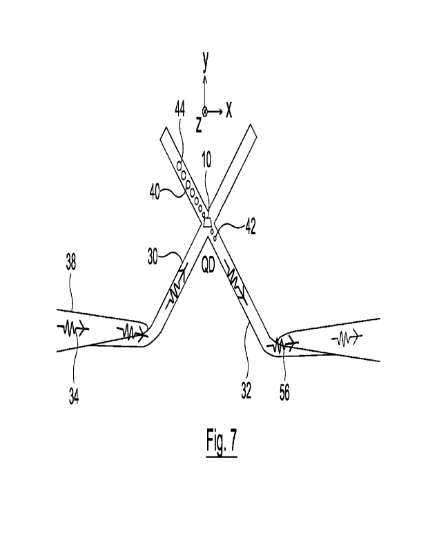
Referring to Figure 7, an alternative arrangement for realising the structure
of Figures
2a and 2b is to form the QD 10, for example of InAs on a layer 16a of, for
example,
10 GaAs as with Figures 5 and 6, but then to form nanobeam waveguides 30,
32 on the
GaAs layer 16a and over the QD 10. Each of the nanobeam waveguides 30, 32
comprises a straight strip of material, which is typically the same as the
layer 16a, and
therefore GaAs, formed by photolithography. Further layers, for example of
AlGaAs,
may be included for their electrical properties. The two waveguides 30, 32
extend in
15 mutually perpendicular directions and cross at the point where the QD 10
is formed.
As with the embodiment of Figures 5 and 6, in this example the QD asymmetry is
pinned to x-y axes, defined by GaAs crystallographic orientation. The
waveguide
photonic structure axes are in-plane, Le. parallel to the plane of the
substrate, but each
oriented at 45 degrees to the x-y axes. The D-aligned waveguide 30 forms the
20 excitation waveguide and is used for delivering trigger laser pulses 34
polarised in the
D direction, and the A-aligned waveguide 32 forms the collection waveguide and
is
used to collect photons 36 polarised in the A direction. Each of the
waveguides 30, 32
may be coupled to the tapered end of an optical fibre 38 through which the
laser
stimulation pulses and collected photons are transmitted to and from the
device.
In order to provide Purcell enhancement of the emission of photons into the
collection
waveguide 32, a resonator may be provided in at least one of the waveguides
30, 32.
For example the excitation waveguide 30, which couples only to the IXD)
transition,
may not be provided with a resonator and. The orthogonal, A-aligned collection
30 waveguide 32, which couples to the IXA) transition may have an
asymmetric photonic
crystal cavity which induces Purcell enhancement. This cavity may be formed by
forming a Bragg reflector 40 on one side of the QD 10, and a weaker Bragg
reflector
42 on the opposite side of the QD 10, with the two reflectors facing each
other. The
Bragg reflector 40 may be formed as a plurality of holes 44 formed in the
waveguide
35 with a regular spacing and aligned along the centre of the waveguide.
This effectively
CA 03150885 2022-3-10
WO 2021/048560
PCT/GB2020/052193
9
prevents any emission of photons along the collection waveguide 32 in one
direction
which is opposite to the collection direction. The weaker Bragg reflector 42
comprises
a similar array of holes, but fewer in number. This allows photons to be
emitted along
the collection waveguide in one direction, which is the collection direction.
The
5 asymmetry of the cavity leads to nearly 100% directional emission of the
single
photons in the collection direction. The excitation waveguide 30 may have no
resonator formed in it at all, as shown in Figure 7, or it may have a low Q
factor
resonator, formed for example as a single hole formed on each side of the QD
10. This
will reduce the laser power required to achieve a "a-pulse", but may also
increase the
10 probability of emission along the excitation waveguide 30.
In addition to the reflector(s) formed in the collection waveguide 32, a pair
of
reflectors may be formed in the excitation waveguide, one on each side of the
QD 10.
In this case the reflectors are arranged to form a resonator with a central
frequency
15 that is detuned from the exciton energy by several times greater than
the spectral
width of the resonator mode. In this way, the emission of the QD into the
excitation
waveguide may be "Purcell supressed", offering potentially even greater
efficiency
into the collection waveguide, though at the expense of requiring additional
excitation
power.
Referring back to Figures 5 and 6, while no resonators are shown in those
figures,
they may be included in the form of further holes in the collection (and
excitation)
waveguides 20, 22 having the same configuration as the holes 44 of Figure 7.
25 The embodiments of Figures 5 to 7, which involve the positioning of an
asymmetric
quantum dot in a particular design of wave guide, enable the input of source
photons
and the output of photons that have the same energy. They also provide an
integrated
on-chip filtering capability that does not require polarisers or spectral
filters (which
compromise the deterministic nature of the SPS by introducing loss) and has a
total
30 efficiency close to unity for realistic parameters. They can therefore
also provide SPSs
with high repetition rate, which is of a crucial importance since it is
essential for
large-scale on-chip photon de-multiplexing, which is an industry target of a
proof-of-
concept on-chip quantum computing device (see e.g. Nature Photon. 11, 361-365
(2017)) and then would be required for the future devices. Also, given that
quantum
35 systems are extremely sensitive to the noise in the environment, the
number of error-
CA 03150885 2022-3-10
WO 2021/048560
PCT/GB2020/052193
free operations decreases exponentially with time, so ten times faster
repetition rate
provides even more dramatic theoretical increase in productivity. Finally, a
higher
repetition rate source also increases both the achievable range and bit-rate
for secure
quantum key distribution (QKD) with single photons.
5
Referring back to Figures 5 and 6, in a further embodiment the quantum dot 10
is
round rather than oval and a magnetic field B is applied in the z direction,
i.e.
perpendicular to the plane of the waveguides. This gives rise to an energy
diagram as
shown in Figure 8. There are two circularly-polarised exciton states, one a+
with the
10 electron spin parallel to the magnetic field and one cr-
with the electron spin anti-
parallel to the magnetic field. The direction of spin of the electron is
represented in
Figure 8 by the simple arrow t and the direction of spin of the hole is
represented by
the open arrow IT. These two states have different energies as shown in Figure
8. The
difference between the two energies is the Zeeman energy, where the Zeeman
energy
Ez = ggB where g is the exciton "g-factor", g is the Bohr magneton and B is
the
magnitude of the applied magnetic field. Referring to Figure 6, if an exciting
photon
is directed along the excitation waveguide, with polarisation in the x-y plane
and
perpendicular to the magnetic field B, then the exciton will have electron and
hole
spin directions perpendicular to the magnetic field. This corresponds to a
linearly
polarised state of the exciton and can be considered as a superposition of the
two
circularly polarised exciton states shown in Figure 8, and this linearly
polarised state
will have an energy which is an average of the energies of the two states
shown in
Figure 8, as shown in Figure 9. Once excited into this state, the electron
(and hole)
will precess about the magnetic field between one state XD which is coupled to
the
excitation waveguide, and another state XA which is coupled to the collection
waveguide. The frequency of precession depends on the strength of the magnetic
field,
and is given by ggB/h rather (rather than 8 in the embodiment of Figures 5 and
6
described above). It will be appreciated that, while the excitation and
collection
waveguides should be mutually perpendicular in this arrangement, to avoid
cross-talk
between them, the waveguides can be at any orientation within the plane of the
photonic crystal structure, relative to the quantum dot.
While the embodiment described above uses a circular quantum dot, a similar
result
can be achieved using an oval quantum dot as shown in Figures la and 2a
provide the
CA 03150885 2022-3-10
WO 2021/048560
PCT/GB2020/052193
11
magnetic field is strong enough so that the Zeeman energy split shown in
Figure 8 is
significantly greater than the fine structure energy split shown in Figure lb.
In further alternative arrangements, rather than a quantum dot 10, other types
of
5 photon emitter may be used in combination with a magnetic field. For
example the
photon emitter may comprise a diamond crystal with a defect, such as a
nitrogen-
vacancy centre or a silicon-vacancy centre. In these defects, in particular
negatively
charged nitrogen-vacancy centres, electrons can be excited into various
exciton states
which can be coupled with polarized light in the excitation and collection
waveguides
in the same way as described above with reference to Figures 5 to 7. In a
structure
similar to that of Figures 5 and 6 with a nitrogen-vacancy centre in diamond
in place
of the QD 10, a magnetic field may be applied in the z direction, i.e.
perpendicular to
the plane of the waveguides, using suitably located electro-magnets, which
gives rise
to two circularly polarized eigenstates as described above with reference to
Figure 8.
15 In this case the device operates in a similar manner to that described
above.
In either of the arrangements described above using a magnetic field, the
structure of
the device may be as shown in Figures 5 and 6, or as shown in Figure 7
20 As a further alternative to the colour centres in diamond, defects in 2D
materials (e.g.
hexagonal boron nitride (hBN)) may also be used as the photon emitter. In this
case
the photonic crystal structure similar to that of Figures 5 and 6 may be
formed of
silicon nitride, and a flake of the 2D material placed on the location of the
quantum
dot 10 of Figures 5 and 6. The 2D emitter then evanescently couples to the
photonic
25 crystal cavity.
While the use of a magnetic field to provide the split energy levels as in
Figure 8 has
the advantage that the magnetic field can easily be varied to control the
energy levels,
the requirement to provide a magnetic field typically makes such systems
larger and
30 more complex than the systems of Figures la to 2b, which therefore have
advantages
in many applications.
CA 03150885 2022-3-10