Note: Descriptions are shown in the official language in which they were submitted.
Terahertz Ferroelectric Resonator
Technical field
The disclosure relates to electrical resonator circuits, in particular to
electrical resonators of
integrated circuits.
Background
The semiconductor industry is driven by its goal to miniaturize integrated
electronic circuitry and
to increase its switching frequencies and speeds. Conventional, silicon-based
integrated circuitry
may at some point hit fundamental limits regarding switching frequencies
dictated by the
capacitance and inductivity of devices and by the energy losses during signal
transmission.
Concepts for faster circuitry and alternative transmission pathways are
desirable. Signal
transmission via electromagnetic waves rather than electronic transmission has
been proposed.
A development from nowadays gigahertz electronics to future terahertz
electronics might allow
for electronic signal processing and electromagnetic wave signal transmission
at similar
frequencies using the same or similar integrated electronic elements.
Therefore, integrated
elements to couple terahertz circuits and the electromagnetic fields are
desirable.
Terahertz electromagnetic signal transmission and in particular reception can
also be useful for
existing applications, such as medical imaging and security screening, or in
long scale signal
transmission, for example in aerospace industry and space or satellite data
communication.
Existing terahertz integrated electronic elements, like resonators required
for signal transmission
and reception, include split ring and split disc type resonators. The
dimensions of these structures
are determined by the terahertz wavelength and much larger than the typical,
critical dimensions
of silicon-based integrated circuitry. Improvements are desirable to allow for
the miniaturization
and cointegration of terahertz oscillators and resonators with miniaturized
integrated circuitry.
1
Date Recue/Date Received 2022-03-03
Overview
In view of the technical problems described above, there is a need for an
improved method for
coupling an oscillation in a terahertz spectral range of electrons of an
electrical circuit or of a
terahertz electromagnetic wave with a resonator, in particular a resonator
which can be
incorporated into a miniaturized integrated circuit.
This objective is achieved with a method according to independent claim 1.
Independent claim 8
provides a device with a heterostructure to be applied as a resonator.
Independent claim 15
provides a method of fabricating a device with a heterostructure suitable to
be applied as a
resonator. The dependent claims relate to preferred embodiments.
In a first aspect, the disclosure relates to a method of employing a device
with a heterostructure
as a resonator for electrons of an electrical circuit or for a terahertz
electromagnetic wave. The
heterostructure comprises at least one dielectric layer and at least one
ferroelectric layer. The at
least one ferroelectric layer comprises a plurality of ferroelectric
polarization domains forming a
polarization pattern. The polarization pattern is adapted to perform an
oscillation with a
resonance frequency in a terahertz frequency range. The method comprises
functionally coupling
the oscillation of the polarization pattern and an oscillation of the
electrons of the electrical circuit
or of the terahertz electromagnetic wave by the device.
The device with the heterostructure comprising at least one dielectric layer
and at least one
ferroelectric layer can be integrated into miniaturized integrated circuitry,
which may provide
advantages over existing terahertz resonators such as split ring resonators
and split disc
resonators. In particular, the lateral area of the device can be miniaturized,
for example to the
critical dimensions of nowadays' semiconductor devices. Moreover, the at least
one ferroelectric
layer and/or the at least one dielectric layer can be deposited using well-
developed techniques of
the layer deposition technology. Advantageously for the miniaturization,
elements to provide
significant inductance can be omitted in the device.
Advantageously, the at least one ferroelectric layer and the at least one
dielectric layer may be
formed from insulating materials, which may show very little response to
oscillations, for example
electromagnetic waves, at frequencies much lower or much higher than the
resonance frequency,
or at the frequencies of the oscillation of the polarization pattern, the
electrons of the electrical
circuit, or of the terahertz electromagnetic wave. This may suppress
undesirable responses and
noise which might otherwise result from the response to oscillations, for
example electromagnetic
waves, at much higher or much lower frequencies.
2
Date Recue/Date Received 2022-03-03
In the context of the present disclosure, a heterostructure may comprise a
sandwich-like
heterostructure or stacked heterostructure, a multilayer structure, and/or a
superlattice.
The resonance frequency may be selected from a plurality of resonance
frequencies of the
heterostructure and/or of the polarization pattern. In particular, the
resonance frequency may
correspond to a principal resonance frequency of the plurality of resonance
frequencies of the
heterostructure and/or of the polarization pattern.
In addition, insulating materials of the at least one ferroelectric layer
and/or the at least one
dielectric layer may reduce the risk of undesirable electrical short
circuiting across the device.
Advantageously, the polarization pattern of the device has a resonance
frequency in the terahertz
spectral range which can be adjusted to the requirements of a specific
application, for example by
selecting suitable thicknesses of the at least one ferroelectric layer or the
at least one dielectric
layer, or by selecting a suitable material composition of the at least one
ferroelectric layer and the
at least one dielectric layer. The resonance frequency can advantageously be
used for resonant
coupling between the oscillation of the polarization pattern and the
oscillation of the electrons of
the electrical circuit or of the terahertz electromagnetic wave. Resonant
coupling provides a
particularly efficient coupling.
In the context of the present disclosure, the terahertz frequency range may
comprise frequencies
of at least 0.05 THz, in particular at least 0.1 THz or at least 0.2 THz.
In the context of the present disclosure, the terahertz frequency range may
comprise frequencies
up to 20 THz, in particular up to ID THz or up to 3 THz.
The oscillation of the polarization pattern can have an oscillation frequency
in a second terahertz
frequency range.
The oscillation of the electrons of the electrical circuit or of the terahertz
electromagnetic wave
can have a coupling frequency in the second terahertz frequency range.
The second terahertz frequency range may comprise frequencies of at least 0.05
THz, in particular
at least 0.1 THz or at least 0.2 THz.
The second terahertz frequency range may comprise frequencies up to 20 THz, in
particular up to
io THz or up to 3 THz.
The oscillation of the polarization pattern and/or the oscillation of the
electrical circuit or of the
terahertz electromagnetic wave with an oscillation frequency or a coupling
frequency not too far
from the resonance frequency of the polarization pattern may advantageously
allow for efficient
3
Date Recue/Date Received 2022-03-03
coupling between the oscillation of the polarization pattern and the
oscillation of the electrical
circuit or of the terahertz electromagnetic wave.
The oscillation of the polarization pattern may have an oscillation frequency,
and the oscillation
of the electrons of the electrical circuit or of the terahertz electromagnetic
wave may have a
coupling frequency, and the coupling frequency may match the oscillation
frequency.
According to an embodiment of the disclosure, the oscillation frequency
matches the resonance
frequency.
The resulting resonant coupling can allow for a particularly efficient
coupling between the
oscillation of the polarization pattern and the oscillation of the electrons
of the electrical circuit
or of the terahertz electromagnetic wave.
According to an embodiment, the coupling frequency matches the resonance
frequency.
The resulting resonant coupling can allow for a particularly efficient
coupling between the
oscillation of the polarization pattern and the oscillation of the electrons
of the electrical circuit
or of the terahertz electromagnetic wave.
Matching frequencies may deviate from one another at most by a factor of 2, in
particular at most
1.5, or at most 1.1.
According to an embodiment, the heterostructure may comprise a plurality of
ferroelectric layers.
The plurality of ferroelectric layers may comprise at least three
ferroelectric layers, in particular
at least five, ten, twenty, or fifty ferroelectric layers.
In particular, the at least one ferroelectric layer may be at least one
ferroelectric layer of the
plurality of ferroelectric layers. The at least one ferroelectric layer may be
or comprise a thickest
ferroelectric layer of the plurality of ferroelectric layers, or a thinnest
ferroelectric layer of the
plurality of ferroelectric layers.
Each ferroelectric layer of the plurality of ferroelectric layers may comprise
a plurality of
ferroelectric polarization domains forming a polarization pattern.
According to an embodiment, each layer of the plurality of ferroelectric
layers may have a same
maximum ferroelectric layer thickness. In particular, each layer of the
plurality of ferroelectric
layers may have a same ferroelectric layer thickness, for example along a line
intersecting the
heterostructure, in particular along a line intersecting the heterostructure
along a direction
perpendicular to the at least one ferroelectric layer.
4
Date Recue/Date Received 2022-03-03
Alternatively or in addition, the heterostructure may comprise a plurality of
dielectric layers. The
plurality of dielectric layers may comprise at least three dielectric layers,
in particular at least five,
ten, twenty, or fifty dielectric layers.
In particular, the at least one dielectric layer may be at least one
dielectric layer of the plurality of
dielectric layers. The at least one dielectric layer may be or comprise a
thickest dielectric layer of
the plurality of dielectric layers, or a thinnest dielectric layer of the
plurality of dielectric layers.
According to an embodiment, each layer of the plurality of dielectric layers
may have a same
maximum dielectric layer thickness. In particular, each layer of the plurality
of dielectric layers
may have a same dielectric layer thickness, for example along a line
intersecting the
heterostructure, in particular along a line intersecting the heterostructure
along a direction
perpendicular to the at least one dielectric layer.
The heterostructure may comprise an alternating stacking sequence of
dielectric layers of the
plurality of dielectric layers and ferroelectric layers of the plurality of
ferroelectric layers.
Alternatively or in addition, the heterostructure may comprise a stacking
sequence with at least
two subsequent ferroelectric layers of the plurality of ferroelectric layers
or with at least two
subsequent dielectric layers of the plurality of dielectric layers.
Alternatively or in addition, the heterostructure may comprise a stacking
sequence with at least
one additional layer between a first layer of the plurality of ferroelectric
layer or of the plurality of
dielectric layers and a second layer of the plurality of the plurality of
ferroelectric layer or of the
plurality of dielectric layers.
A plurality of ferroelectric layers and/or a plurality of dielectric layers
can increase the coupling
volume and hence the strength of the coupling between the oscillation of the
polarization pattern
and the oscillation of the electrical circuit or of the terahertz
electromagnetic wave.
According to an embodiment, the method further comprises employing the device
as a component
of a receiver or a transmitter for the terahertz electromagnetic wave.
Employing the device as a component of the receiver or the transmitter
advantageously makes
use of the coupling between the oscillation of the polarization pattern and
the coupling of the
electrons of the electrical circuit. This may be particularly useful for
applications of the device
related to inter-chip and/or intra-chip signal transmission and/or processing,
6G WiFi
communication, and/or satellite communication.
5
Date Recue/Date Received 2022-03-03
According to an embodiment, the heterostructure is functionally coupled to a
diode or a
transistor. In particular, the device may be a component of the receiver, and
the diode or the
transistor serves as a rectifier.
As the device with the heterostructure can be integrated together with
miniaturized
semiconductor devices like the transistor and/or the diode, these well-
established semiconductor
devices can advantageously be used to implement a driver and/or a readout
circuit for the
resonator.
According to an embodiment, the device is a first component of a common
integrated circuit and
the diode or the transistor is a second component of the common integrated
circuit. For example,
the first component of the common integrated circuit and the second component
of the common
integrated circuit may be arranged on a common substrate. For example, the
common substrate
may be a semiconductor or dielectric substrate. In particular, the
semiconductor or dielectric
substrate may be a semiconductor or dielectric wafer.
According to an embodiment, the first component of the common integrated
circuit and the
second component of the common integrated circuit are arranged in direct
physical contact with
each other.
At least a layer of the device and at least a section of the second component
of the common
integrated circuit may be composed of the same material. The same material
composition of the
layer of the device and the section of the second component of the common
integrated circuit may
by the result of a common deposition step.
The device may be functionally coupled to an additional antenna. In
particular, the additional
antenna may be a split ring resonator or a split disc resonator.
According to an embodiment, the method further comprises applying the device
as a component
of an RC circuit. In particular, the device may be employed as a capacitor of
the RC circuit.
The implementation of an RC circuit comprising the device provides a resonator
with the potential
to be highly miniaturized and integrated. In particular, the implementation as
an RC circuit
permits to omit significant inductances, which tend to require large lateral
areas is in the layout
of an integrated circuit.
The RC circuit may comprise a resistor in parallel or in series with the
heterostructure. According
to an embodiment, the device is a first component of a common integrated
circuit, and the resistor
is a second component of the common integrated circuit.
6
Date Recue/Date Received 2022-03-03
The device and a resistor can advantageously be formed as components of a
common integrated
circuit.
The common integrated circuit, the first component of the common integrated
circuit, and the
second component of the common integrated circuit may be characterized by
features
corresponding to the ones described in the context of a diode or a transistor
forming the second
component of the common integrated circuit.
The device may be employed as a component of a low pass filter, a high pass
filter, or a band pass
filter.
In particular, the RC circuit comprising the device as a component may be
employed as a
component of a low pass filter, a high pass filter, or a band pass filter.
The low pass filter, the high pass filter, or the band pass filter can have a
cutoff frequency in a
cutoff frequency range.
The band pass filter can have a second cutoff frequency in the cutoff
frequency range.
The cutoff frequency range may comprise frequencies of at least 0.1 THz, in
particular at least
1 THz or at least 0.2 THz.
The cutoff frequency range may comprise frequencies up to 1,00 THz, in
particular up to 10 THz.
The low pass filter, the high pass filter, or the band pass filter may be an
electronic low pass filter,
an electronic high pass filter, or an electronic band pass filter.
The device may be employed as a component of a clock.
The device advantageously provides a resonance frequency in the terahertz
frequency range,
which is just above the frequency range being used by current electronics, and
thus may permit
to implement clocks operating at higher frequency and thus at higher
precisions than the ones
currently used in semiconductor devices.
Employing the device as a component of the clock may comprise determining a
maximum or a
minimum of a parameter that characterizes the oscillation of the polarization
pattern.
Employing the device as a component of the clock may comprise counting a
plurality of maxima
or minima, wherein each maximum or minimum is a maximum or a minimum of the
parameter
related to the oscillation of the polarization pattern.
7
Date Recue/Date Received 2022-03-03
The parameter related to the oscillation of the polarization pattern may be a
measure of the total
polarization of the polarization pattern or a measure of the change of the
total polarization of the
polarization pattern.
The parameter related to the oscillation of the polarization pattern may be a
measure of a local
polarization of the polarization pattern, or a measure of the change of a
local polarization of the
polarization pattern.
The device may further comprise a second heterostructure comprising at least
one second
dielectric layer and at least one second ferroelectric layer. The second
ferroelectric layer may
comprise a second plurality of ferroelectric polarization domains forming a
second polarization
pattern, and the second polarization pattern may be adapted to perform a
second oscillation with
a second resonance frequency in the terahertz frequency range. Applying the
device may further
comprise employing the heterostructure as a component of a transmitter adapted
to generate a
transient terahertz electromagnetic wave, and employing the second
heterostructure as a
component of a receiver to receive the transient terahertz electromagnetic
wave. This may be
particularly useful for applications of the device related to intra-chip
signal transmission and/or
processing.
The second heterostructure may comprise a second plurality of ferroelectric
layers. The plurality
of ferroelectric layers may comprise at least three ferroelectric layers, in
particular at least five,
ten, twenty, or fifty ferroelectric layers.
According to an embodiment, the at least one second ferroelectric layer may be
at least one
ferroelectric layer of the second plurality of ferroelectric layers. The at
least one second
ferroelectric layer may be or comprise a thickest ferroelectric layer of the
second plurality of
ferroelectric layers, or a thinnest ferroelectric layer of the second
plurality of ferroelectric layers.
In particular, each layer of the second plurality of ferroelectric layers may
have a same second
maximum ferroelectric layer thickness. In particular, each layer of the second
plurality of
ferroelectric layers may have a same second ferroelectric layer thickness, for
example along a line
intersecting the second heterostructure, in particular along a line
intersecting the second
heterostructure along a direction perpendicular to the second ferroelectric
layer.
Alternatively, or in addition, the second heterostructure may comprise a
second plurality of
dielectric layers. The plurality of dielectric layers may comprise at least
three ferroelectric layers,
in particular at least five, ten, twenty, or fifty dielectric layers.
8
Date Recue/Date Received 2022-03-03
According to an embodiment, the at least one second dielectric layer may be a
dielectric layer of
the second plurality of dielectric layers. The at least one second dielectric
layer may be or comprise
a thickest dielectric layer of the second plurality of dielectric layers, or a
thinnest dielectric layer
of the second plurality of dielectric layers.
In particular, each layer of the second plurality of dielectric layers may
have a same second
maximum dielectric layer thickness. In particular, each layer of the second
plurality of dielectric
layers may have a same second dielectric layer thickness, for example along a
line intersecting the
second heterostructure, in particular along a line intersecting the second
heterostructure along a
direction perpendicular to the at least one second dielectric layer.
According to an embodiment, the heterostructure is a first component of a
common integrated
circuit, and the second heterostructure is a second component of the common
integrated circuit.
The common integrated circuit, the first component of the common integrated
circuit, and the
second component of the common integrated circuit may be characterized by
features
corresponding to the ones described in the context of a diode or a transistor
forming the second
component of the common integrated circuit.
The method may further comprise guiding the transient terahertz
electromagnetic wave using a
waveguide structure.
The method may further comprise guiding the transient terahertz
electromagnetic wave using a
metallic channel, in particular a metallic channel serving as a plasmonic
interconnect channel.
A waveguide structure and/or a plasmonic interconnect channel may be
particularly useful for
applications of the device related to intra-chip signal transmission and/or
processing.
The method may further comprise using the device as a component of a terahertz
optical device
to manipulate the terahertz electromagnetic wave and to control at least one
terahertz optical
parameter.
For example, the terahertz optical device may be a mirror to reflect the
terahertz electromagnetic
wave, and the terahertz optical parameter may be a reflectance.
For example, the terahertz optical device may be an attenuator to transmit a
portion of the
terahertz electromagnetic wave, and the terahertz optical parameter may be an
attenuation.
For example, the terahertz optical device may be a beam splitter to reflect a
portion of the
.. terahertz electromagnetic wave and to transmit another portion of the
terahertz electromagnetic
9
Date Recue/Date Received 2022-03-03
wave, wherein the terahertz optical parameter is a reflectance and a second
terahertz optical
parameter may be a transmittance.
For example, the terahertz optical device may be a phase shifter to modify a
phase of the terahertz
electromagnetic wave, and the terahertz optical parameter may be a phase
shift.
For example, the terahertz optical device may be a terahertz optical low pass
filter, a terahertz
optical high pass filter, or a terahertz optical bandpass filter for the
terahertz electromagnetic
wave, and the terahertz optical parameter may be a cutoff frequency.
Advantageously, techniques for the design of layered dielectric optics can be
used to tailor the
terahertz optical device to match the requirements of specific application,
for example as a mirror,
a beam splitter, an attenuator, a phase shifter, a dichroic mirror, a
(terahertz) optical high pass
filter, a (terahertz) optical low pass filter, a (terahertz) band pass filter,
or as a (terahertz) optical
notch filter.
For example, the terahertz optical device may be a guiding structure for the
terahertz
electromagnetic wave, and the terahertz optical parameter may be a direction
of the terahertz
electromagnetic wave. In particular, the terahertz optical device may comprise
a terahertz optical
metamaterial to guide the terahertz electromagnetic wave inside the
heterostructure.
A thickness of the at least one ferroelectric layer may be adapted to control
the terahertz optical
parameter.
The method may further comprise applying a static electric field to the
heterostructure to control
the terahertz optical parameter.
The method may further comprise triggering the oscillation of the electrons of
the electrical circuit
to control the terahertz optical parameter.
The method may further comprise applying a mechanical stress to the
heterostructure to control
the terahertz optical parameter.
The heterostructure may be a first component of a common integrated circuit,
and an additional
terahertz optical device or an additional terahertz optoelectronic device may
be a second
component of the common integrated circuit.
The common integrated circuit, the first component of the common integrated
circuit, and the
second component of the common integrated circuit may be characterized by
features
Date Recue/Date Received 2022-03-03
corresponding to the ones described in the context of a diode or a transistor
as the second
component of the common integrated circuit.
The method may further comprise employing the device as a component of a
receiver or a
transmitter for the terahertz electromagnetic wave, in addition to using the
device as a component
of a terahertz optical device to manipulate the terahertz electromagnetic wave
and to control at
least one terahertz optical parameter.
In a second aspect, the disclosure relates to a device with a heterostructure
adapted to be applied
as a resonator for electrons of an electrical circuit or for a terahertz
electromagnetic wave. The
heterostructure comprises at least one dielectric layer and at least one
ferroelectric layer. The
ferroelectric layer comprises a plurality of ferroelectric polarization
domains forming a
polarization pattern. The polarization pattern is adapted to execute an
oscillation with a resonance
frequency in a terahertz frequency range. The device is adapted to couple the
oscillation of the
polarization pattern with an oscillation at a coupling frequency of the
electrons of the electrical
circuit or of the terahertz electromagnetic wave. The oscillation of the
polarization pattern has an
oscillation frequency in a second terahertz frequency range.
The device with the heterostructure can advantageously be applied in a method
comprising at
least some of the features described above.
The terahertz frequency range and/or the second terahertz frequency range may
be defined as in
the context of the first aspect of the disclosure.
The heterostructure may comprise a plurality of ferroelectric layers. The
plurality of ferroelectric
layers may comprise at least three ferroelectric layers, in particular at
least five, ten, twenty, or
fifty ferroelectric layers.
According to an embodiment, the at least one ferroelectric layer may be at
least one ferroelectric
layer of the plurality of ferroelectric layers. The at least one ferroelectric
layer may be or comprise
a thickest ferroelectric layer of the plurality of ferroelectric layers, or a
thinnest ferroelectric layer
of the plurality of ferroelectric layers.
In particular, each layer of the plurality of ferroelectric layers may have a
same maximum
ferroelectric layer thickness. In particular, each layer of the plurality of
ferroelectric layers may
have a same ferroelectric layer thickness, for example along a line
intersecting the
heterostructure, in particular along a line intersecting the heterostructure
along a direction
perpendicular to the at least one ferroelectric layer.
11
Date Recue/Date Received 2022-03-03
Alternatively, or in addition, the heterostructure may comprise a plurality of
dielectric layers. The
plurality of dielectric layers may comprise at least three dielectric layers,
in particular at least five,
ten, twenty, or fifty dielectric layers.
According to an embodiment, the at least one dielectric layer may be at least
one dielectric layer
of the plurality of dielectric layers. The at least one dielectric layer may
be or comprise a thickest
dielectric layer of the plurality of dielectric layers or a thinnest
dielectric layer of the plurality of
dielectric layers.
In particular, each layer of the plurality of dielectric layers may have a
same maximum dielectric
layer thickness. In particular, each layer of the plurality of dielectric
layers may have a same
dielectric layer thickness, for example along a line intersecting the
heterostructure, in particular
along a line intersecting the heterostructure along a direction perpendicular
to the at least one
dielectric layer.
The heterostructure can have a height of at least 5 nm, in particular of at
least roo nm, in
particular of at least 500 nm, in particular of at least 1 jam.
The heterostructure may cover a lateral area of at most 25 mm2, in particular
of at most 5001=2,
in particular of at most roo pm2, or of at most ro 1=2, or at most 25 nm2.
The polarization pattern may have a spatial periodicity along a lateral
direction of the at least one
ferroelectric layer. In particular, the polarization pattern may be a periodic
polarization pattern.
According to an embodiment, a thickness of the at least one ferroelectric
layer does not exceed
roo nm, in particular 70 nm, 40 nm, 30 nm or 5 nm.
In general, several or all ferroelectric layers of the plurality of
ferroelectric layers may have an
identical thickness. In other embodiments, a thickness of several or all
ferroelectric layers of the
plurality of ferroelectric layers may differ.
In embodiments with a plurality of ferroelectric layers, a thickness of some
or any of the
ferroelectric layers comprised in the plurality of ferroelectric layers may
not exceed roo nm, in
particular 70 nm, 40 nm, 30 nm or 5 nm.
The at least one ferroelectric layer may comprise lead titanate, barium
titanate, zirconium oxide
or hafnium oxide. In embodiments with a plurality of ferroelectric layers, a
first ferroelectric layer
of the plurality of ferroelectric layers and a second ferroelectric layer of
the plurality of
ferroelectric layers may be composed of the same material or of different
materials.
12
Date Recue/Date Received 2022-03-03
According to an embodiment, a thickness of the at least one dielectric layer
comprised in the
plurality of dielectric layers does not exceed 100 nm, in particular 70 nm, 40
nm, 30 nm or 5 nm.
In general, several or all dielectric layers of the plurality of dielectric
layers may have an identical
thickness. In other embodiments, a thickness of several or all dielectric
layers of the plurality of
dielectric layers may differ.
In embodiments with a plurality of dielectric layers, a thickness of some or
any of the dielectric
layers comprised in the plurality of dielectric layers may not exceed loo nm,
in particular 70 nm,
40 nm, 30 nm or 5 nm.
The at least one dielectric layer may comprise insulating material, for
example strontium titanate.
In embodiments with a plurality of dielectric layers, a first dielectric layer
of the plurality of
dielectric layers and a second dielectric layer of the plurality of dielectric
layers may be composed
of the same material, or of different materials.
The device may further comprise a bottom electrode arranged below the
heterostructure.
In particular, in embodiments with a plurality of dielectric layers and/or a
plurality of ferroelectric
layers, the bottom electrode may be arranged below the plurality of dielectric
layers and/or below
the plurality of ferroelectric layers.
The device may further comprise a top electrode arranged above the
heterostructure. In
particular, in embodiments with a plurality of dielectric layers and/or a
plurality of ferroelectric
layers, the top electrode may be arranged above the plurality of dielectric
layers and/or above the
plurality of ferroelectric layers.
The device may further comprise at least one intermediate electrode arranged
between an
intermediate top layer and an intermediate bottom layer.
In embodiments with a heterostructure comprising one dielectric layer and one
ferroelectric layer,
the intermediate top layer may be the ferroelectric layer or the dielectric
layer, and the
intermediate bottom layer may be the dielectric layer or the ferroelectric
layer, respectively.
In embodiments with a plurality of dielectric layers, the intermediate bottom
layer may be a
dielectric layer from the plurality of dielectric layers, and/or the
intermediate top layer may be a
dielectric layer from the plurality of dielectric layers.
13
Date Recue/Date Received 2022-03-03
In embodiments with a plurality of ferroelectric layers, the intermediate
bottom layer may be a
ferroelectric layer from the plurality of ferroelectric layers, and/or the
intermediate top layer may
be a ferroelectric layer from the plurality of ferroelectric layers.
The structure and material composition of the intermediate electrode may
generally correspond
to those of the bottom electrode and top electrode described above.
An intermediate electrode located within the heterostructure may allow for
more versatile
application of the resonator.
Each of the bottom electrode, top electrode and bottom electrode may be
adapted to be connected
to an external driving circuitry, or to ground.
.. The heterostructure may be arranged above a substrate.
The substrate may be structured to promote the formation of the device.
Advantageously,
additional elements may be formed on the same device to implement complex
integrated
circuitry. Moreover, the device may be selected to promote the formation of at
least one layer of
the device, for example via the wetting properties of the substrate or via
epitaxial growth of at
least one layer of the device on the substrate.
The substrate may be a semiconductor or dielectric substrate.
Semiconductor or dielectric substrates are well developed, available at
moderate pricing, and the
formation of a layer on semiconductor or dielectric substrates has been highly
developed in the
context of layer deposition technology.
The substrate may comprise a single crystalline section with a lateral
dimension at least as large
as a lateral dimension of the heterostructure. In particular, the substrate
may be adapted to
promote epitaxial growth of the at least one dielectric layer or of the at
least one ferroelectric layer.
Crystalline sections of the substrate may promote epitaxial growth of at least
one layer of the
device. Epitaxial growth tends to minimize the density of defects in the
layer.
The device may be a mechanically flexible device.
In particular, the device may be a free-standing device.
The device may further comprise an additional integrated element, wherein the
heterostructure
is a first component of a common integrated circuit, and the additional
integrated element is a
second component of the common integrated circuit.
14
Date Recue/Date Received 2022-03-03
The common integrated circuit, the first component of the common integrated
circuit, and the
second component of the common integrated circuit may be characterized by
features
corresponding to the ones described in the context of the method with a diode
or a transistor as
the second component of the common integrated circuit.
For example, the additional integrated element may be a resistor. The resistor
may be arranged
in series or in parallel with the heterostructure.
For example, the additional integrated element may be a diode or a transistor.
The diode or
transistor may be functionally coupled to the heterostructure.
For example, the additional integrated element may be an additional terahertz
optical device or
an additional terahertz optoelectronic device.
For example, the additional integrated element may be an additional antenna
coupled to the
heterostructure.
In particular, the additional antenna may be a split ring resonator or a split
disc resonator.
The device may further comprise a plurality of integrated elements, wherein
each integrated
element of the plurality of integrated elements may be a component of the
common integrated
circuit.
The device may further comprise a second heterostructure adapted to be applied
as a second
resonator for electrons of a second electrical circuit or for a second
terahertz electromagnetic
wave. The second heterostructure may comprise at least one dielectric layer
and at least one
second ferroelectric layer. The at least one second ferroelectric layer may
comprise a second
plurality of ferroelectric polarization domains forming a second polarization
pattern. The second
polarization pattern may be adapted to execute a second oscillation with a
second resonance
frequency in the terahertz frequency range. The device may be adapted to
couple the second
oscillation of the second polarization pattern with a third oscillation at a
second coupling
frequency of the electrons of the second electrical circuit or of the second
terahertz
electromagnetic wave. The second oscillation of the second polarization
pattern may have a
second oscillation frequency in the second terahertz frequency range.
In some embodiments, the design and features of the second heterostructure may
correspond to
those of the heterostructure described above, such as in terms of the layout,
the number and
position of the ferroelectric layers and the dielectric layers, the layer
thicknesses and material
composition.
Date Recue/Date Received 2022-03-03
The second heterostructure may comprise a second plurality of ferroelectric
layers. The plurality
of ferroelectric layers may comprise at least three ferroelectric layers, in
particular at least five,
ten, twenty, or fifty ferroelectric layers.
In particular, the at least one second ferroelectric layer may be at least one
ferroelectric layer of
the second plurality of ferroelectric layers. The at least one second
ferroelectric layer may be or
comprise a thickest ferroelectric layer of the second plurality of
ferroelectric layers, or a thinnest
ferroelectric layer of the second plurality of ferroelectric layers.
According to an embodiment, each layer of the second plurality of
ferroelectric layers may have a
same second maximum ferroelectric layer thickness. In particular, each layer
of the second
plurality of ferroelectric layers may have a same second ferroelectric layer
thickness, for example
along a line intersecting the second heterostructure, in particular along a
line intersecting the
second heterostructure along a direction perpendicular to the at least one
second ferroelectric
layer.
Alternatively, or in addition, the second heterostructure may comprise a
second plurality of
dielectric layers. The plurality of dielectric layers may comprise at least
three ferroelectric layers,
in particular at least five, ten, twenty, or fifty dielectric layers.
In particular, the at least one second dielectric layer may be at least one
dielectric layer of the
second plurality of dielectric layers. The at least one second dielectric
layer may be or comprise a
thickest dielectric layer of the second plurality of dielectric layers, or a
thinnest dielectric layer of
.. the second plurality of dielectric layers.
According to an embodiment, each layer of the second plurality of dielectric
layers may have a
same second maximum dielectric layer thickness. In particular, each layer of
the second plurality
of dielectric layers may have a same second dielectric layer thickness, for
example along a line
intersecting the second heterostructure, in particular along a line
intersecting the second
.. heterostructure along a direction perpendicular to the at least one second
dielectric layer.
The second resonance frequency may be selected from a second plurality of
resonance frequencies
of the second heterostructure and/or of the second polarization pattern.
In particular, the second resonance frequency may correspond to a principal
resonance frequency
of the second plurality of resonance frequencies of the second heterostructure
and/or of the
second polarization pattern.
The second resonance frequency may match the resonance frequency.
16
Date Recue/Date Received 2022-03-03
Matching frequencies may deviate from one another at most by a factor of 2, in
particular at most
1.5, or at most 1.1.
The second terahertz electromagnetic wave and the terahertz electromagnetic
wave may be
identical, and the device may be adapted to couple the oscillation of the
polarization pattern and
the second oscillation of the second polarization pattern using the terahertz
electromagnetic wave.
In a third aspect, the disclosure relates to a method of fabricating a device
with a heterostructure.
The device with the heterostructure is suitable to be applied as a resonator
for electrons of an
electrical circuit or for a terahertz electromagnetic wave. The method
comprises depositing at
least one ferroelectric layer and at least one dielectric layer, wherein a
ferroelectric layer thickness
of the at least one ferroelectric layer does not exceed a predefined maximum
thickness, such that
the at least one ferroelectric layer comprises a plurality of ferroelectric
polarization domains
forming a polarization pattern adapted to perform an oscillation with a
resonance frequency. The
method further comprises adjusting the predefined maximum thickness to a
resonance frequency
in a terahertz frequency range.
The method may further comprise depositing a plurality of ferroelectric
layers. For example,
depositing a plurality of ferroelectric layers may comprise depositing at
least three ferroelectric
layers, in particular at least five, ten, twenty, or fifty ferroelectric
layers.
In particular, the at least one ferroelectric layer may be comprised in the
plurality of ferroelectric
layers. The at least one ferroelectric layer may be deposited to be or
comprise a thickest
ferroelectric layer of the plurality of ferroelectric layers or a thinnest
ferroelectric layer of the
plurality of ferroelectric layers.
According to an embodiment, each layer of the plurality of ferroelectric
layers may be deposited
with a same ferroelectric layer thickness, for example along a line
intersecting the heterostructure,
in particular along a line intersecting the heterostructure along a direction
perpendicular to the
at least one ferroelectric layer.
Alternatively, or in addition, the method may comprise depositing a plurality
of dielectric layers.
For example, depositing a plurality of dielectric layers may comprise
depositing at least three
dielectric layers, in particular at least five, ten, twenty, or fifty
dielectric layers.
In particular, the plurality of dielectric layers may comprise the at least
one dielectric layer. The
at least one dielectric layer may be deposited to be or comprise a thickest
dielectric layer of the
plurality of dielectric layers, or a thinnest dielectric layer of the
plurality of dielectric layers.
17
Date Recue/Date Received 2022-03-03
According to an embodiment, each layer of the plurality of dielectric layers
may be deposited with
a same dielectric layer thickness, for example along a line intersecting the
heterostructure, in
particular along a line intersecting the heterostructure along a direction
perpendicular to the at
least one dielectric layer.
The predefined maximum thickness may comprise a largest thickness of the at
least one
ferroelectric layer along a lateral direction of the heterostructure.
In embodiments with a top electrode and a bottom electrode, the predefined
maximum thickness
may comprise the largest thickness of the at least one ferroelectric layer in
a volume between the
top electrode and the bottom electrode.
In embodiments with a plurality of ferroelectric layers, the predefined
maximum thickness may
be a thickness of a thickest ferroelectric layer of the plurality of
ferroelectric layers along a line
intersecting the heterostructure, in particular along a line perpendicular to
the plurality of
ferroelectric layers.
In embodiments with a top electrode and a bottom electrode and a plurality of
ferroelectric layers,
the predefined maximum thickness may comprise a thickness of a thickest
ferroelectric layer of
the plurality of ferroelectric layers along a line connecting the bottom
electrode and the top
electrode, in particular a line perpendicular to the bottom electrode and the
top electrode.
Alternatively, or in addition, the method may comprise adjusting a ratio of
the ferroelectric layer
thickness and a dielectric constant of the at least one ferroelectric layer.
The terahertz frequency range may comprise frequencies of at least 0.05 THz,
in particular at least
0.1 THz or at least 0.2 THz.
The terahertz frequency range may comprise frequencies up to 20 THz, in
particular up to m THz
or up to 3 THz.
According to an embodiment, adjusting the predefined maximum thickness
comprises selecting
the predefined maximum thickness in accordance with a material constant of a
material
comprised in the at least one ferroelectric layer. In particular, the material
constant of the material
comprised in the at least one ferroelectric layer may be the dielectric
constant of the material
comprised in the at least one ferroelectric layer.
Adjusting the predefined maximum thickness may comprise selecting the
predefined maximum
thickness in accordance with a lateral area of the at least one ferroelectric
layer.
18
Date Recue/Date Received 2022-03-03
Adjusting the predefined maximum thickness may comprise selecting the
predefined maximum
thickness in accordance with a dielectric constant of a material comprised in
the at least one
dielectric layer.
Adjusting the predefined maximum thickness may comprise selecting the
predefined maximum
thickness in accordance with a thickness of the at least one dielectric layer.
In embodiments with a plurality of dielectric layers and/or a plurality of
ferroelectric layers,
adjusting the predefined maximum thickness may comprise selecting the
predefined maximum
thickness in accordance with a number of the dielectric layers and/or a number
of the ferroelectric
layers.
Adjusting the predefined maximum thickness may comprise selecting the
predefined maximum
thickness in accordance with an average size of the ferroelectric polarization
domains.
Adjusting the predefined maximum thickness may comprise selecting the
predefined maximum
thickness in accordance with a size distribution of the ferroelectric
polarization domains.
Brief description of the figures
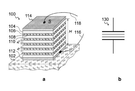
Fig. la shows a Terahertz Ferroelectric Resonator (TFR) according to an
embodiment of the
disclosure, with a thickness ha of an individual dielectric layer, a thickness
hf of an individual
ferroelectric layer, an overall thickness H of a heterostructure, and an area
of a top surface S.
Fig. ib shows an electronic graphical symbol for the Terahertz Ferroelectric
Resonator (TFR).
Fig. 2a shows a heterostructure of the Terahertz Ferroelectric Resonator (TFR)
with a periodic
polarization pattern with stripes according to an embodiment of the
disclosure.
Fig. 2b shows a heterostructure of the Terahertz Ferroelectric Resonator (TFR)
with a cylindrical,
or bubble-like periodic polarization pattern according to another embodiment
of the disclosure.
Fig. 3 shows an exemplary frequency-dependence of the real part Re E and the
imaginary part Im E
of a dielectric constant of a heterostructure of a Terahertz Ferroelectric
Resonator (TFR) with a
thickness hf of an individual ferroelectric layer of 25 nm according to an
embodiment of the
disclosure.
Fig. 4 shows an exemplary frequency-dependence of the resonance frequency of a
heterostructure
of a Terahertz Ferroelectric Resonator (TFR) according to an embodiment of the
disclosure.
19
Date Recue/Date Received 2022-03-03
Fig. 5 shows exemplary frequency-dependences of impedance amplitudes of the
Terahertz
Ferroelectric Resonators (TFRs) for different thicknesses, hi, h2, h3,
according to three
embodiments of the disclosure, where hi corresponds to hf = ha = io nm, h2
corresponds to hf
= hd = 15 nm, and h3 corresponds to hf = ha = 20 nm.
Fig. 6 shows a system for satellite communication comprising a Terahertz
Ferroelectric Resonator
(TFR) according to an embodiment of the disclosure.
Fig. 7 shows a system for 6G wireless communication comprising a Terahertz
Ferroelectric
Resonator (TFR) according to an embodiment of the disclosure.
Fig. 8 shows an integrated circuit comprising a Terahertz Ferroelectric
Resonator (TFR)
according to an embodiment of the disclosure.
Fig. 9a shows an integrated circuit comprising a Terahertz Ferroelectric
Resonator (TFR) and a
load resistor integrated in series according to another embodiment of the
disclosure.
Fig. 9b shows a circuit diagram of the integrated circuit of Fig. 9a.
Fig. 9c shows an integrated circuit comprising a Terahertz Ferroelectric
Resonator (TFR) and a
.. load resistor integrated in parallel according to yet another embodiment of
the disclosure.
Fig. 9d shows a circuit diagram of the integrated circuit of Fig. 9c.
Fig. io shows two communicating Terahertz Ferroelectric Resonators (TFR)
according to yet
another embodiment of the disclosure.
Fig. lia shows a circuit diagram of an integrated circuit for high-pass and
low-pass frequency
filtering based on a Terahertz Ferroelectric Resonator (TFR) according to yet
another
embodiment of the disclosure.
Fig. iib shows the exemplary frequency-dependent output characteristics of a
high pass filter
according to the integrated circuit of Fig. lia for different load
resistances, comprising a Terahertz
Ferroelectric Resonator (TFR) with hf = io nm, hd = 5 nm, H = i p.m and S =
ioo p.m2.
Fig. iic shows the exemplary frequency-dependent output characteristics of a
low pass filter
according to the integrated circuit of Fig. lia for different load
resistances, comprising a Terahertz
Ferroelectric Resonator (TFR) with hf = io nm, hd = 5 nm, H = i p.m and S =
ioo p.m2.
Fig. 12 shows a terahertz optical device according to an embodiment of the
disclosure.
Date Recue/Date Received 2022-03-03
Fig. 13a shows the frequency-dependent refractive index of a terahertz optical
device with with hf
= hd = 25 nm according to an embodiment of the disclosure, in terms of its
real part Re n and its
imaginary part Im n.
Fig. 13b shows the terahertz frequency-dependent optical reflection
coefficient Ro at normal
incidence of a terahertz optical device with with hf = hd = 25 nm according to
an embodiment of
the disclosure.
Detailed description
The present disclosure relates to a device with a heterostructure comprising a
plurality of
ferroelectric layers. The device may provide a strong frequency dependence of
the dielectric
permittivity within a terahertz (THz) frequency range.
The terahertz frequency is not uniquely defined, and in the context of the
present disclosure may
be understood to start at a frequency of 0.05 THz, in particular 0.1 THz or
0.2 THz.
Correspondingly, the terahertz frequency range may comprise frequencies up to
20 THz, in
particular up to 10 THz or up to 3 THz. According to one possible definition,
a THz spectral range
may correspond to wavelengths in a range from 1 mm to 0.1 mm. The terahertz
electromagnetic
spectrum may generally be understood to lie between microwaves and far
infrared.
The device with a heterostructure according to claim 1 will in the following
be explained by way
of the example of a Terahertz Ferroelectric Resonator (TFR).
Fig. la illustrates an example of a TFR loco. The exemplary TFR loco comprises
a heterostructure,
which may be a sandwich-like heterostructure, a multilayer structure, or a
superlattice. The
heterostructure may be deposited, for instance, on a dielectric or
semiconductor substrate 102.
The TFR loco comprises an alternating sequence of layers, including a
plurality of dielectric layers
104 and a plurality of ferroelectric layers 106. The example TFR mo of Fig. la
comprises six
dielectric layers 104 and five ferroelectric layers 106, but other embodiments
of the TFR loco may
comprise different numbers of layers, for example one ferroelectric layer and
one dielectric layer,
or any other number of ferroelectric layers and/or dielectric layers,
depending on the application.
The heterostructure of the TFR loco can be realized, for example, as an
epitaxial grown
superlattice wherein one, several or all of the dielectric layers 104 are
mostly composed of SrTiO3
perovskite oxide and one, several or all the ferroelectric layers 106 are
mostly composed of PbTiO3
perovskite oxide. Alternatively, the ferroelectric layers 106 may for example
comprise other
21
Date Recue/Date Received 2022-03-03
oxides with the perovskite structure, such as barium titanate or lead
zirconium titanate, or non-
perovskite oxides, such as zirconium oxide or hafnium oxide, in particular
doped hafnium oxide.
Other material compositions, comprising, for example, halides, are possible.
A typical thickness ha of an individual layer of the dielectric layers 104 and
typical thickness hf
of the ferroelectric layers 106 can be in a range from a few nm to tens of nm.
The number of
dielectric layers 104 and the number of ferroelectric layers 106 can vary from
a few to tens to
hundreds or even more. In the example, the overall thickness H of the
dielectric layers 104 and
ferroelectric layers 106, and the lateral area of the device, which may be
related to the area of the
top surface S of the device, do not exceed the characteristic terahertz
wavelength in the
heterostructure AI\17 -= 10 um (with the dielectric constant E '=' 100 and A -
= 10 Optm for the
wavelength of an electromagnetic wave with the frequency of 3 THz terahertz in
vacuum) to avoid
parasite inductivity.
The ferroelectric material possesses ferroelectric polarization domains 108,
no with uniaxial
anisotropy of the polarization, which may either occur naturally or be strain-
induced and/or be
tailored by strain engineering. For this purpose, an epitaxial relationship
between the dielectric
layers 104 in the ferroelectric layers 106 may be useful, although not
necessary. Moreover, a
dielectric relationship between the dielectric layer 104 or the ferroelectric
layers 106 and the
substrate 102 may be useful, but not necessary.
According to the example depicted in Fig. ra, the polarization of the
ferroelectric polarization
domains 108, no is directed along the z-axis, which is defined along the
surface normal of the
layers of the heterostructure. Other orientations of the polarization are,
however, possible.
The ferroelectric layers 106 of the heterostructure of Fig. ra are insulating,
and the
heterostructure is insulating. It is confined in between a bottom electrode
112 and a top electrode
114. Each of the bottom electrode 112 and the top electrode 114 can have a
thickness in the range
from 1 to ro nm and comprises metallic or semiconducting material. The
combination of the
bottom electrode 112, the top electrode 114, and the heterostructure with the
dielectric layers 104
and the ferroelectric layers 106 can be viewed as an effective capacitor. The
TFR loo can for
example be produced by subsequent and/or alternating deposition of the
dielectric layers 104
and the ferroelectric layers 106 on the substrate 102. In this case, the
bottom electrode 112 is
deposited on the substrate 102 prior to the deposition of the heterostructure.
Consequently, at
least a portion of the bottom electrode 112 is arranged between the substrate
102 and the
heterostructure of the TFR loo. The top electrode 114 can be fabricated above
the heterostructure
in an additional deposition process after the deposition of the
heterostructure. A bottom contact
22
Date Recue/Date Received 2022-03-03
116 can be attached to the bottom electrode 112, and a top contact 118 can be
attached to the top
electrode 114 for implementation of the electrical connection with an external
circuit.
Fig. ib illustrates the electronic graphical symbol 130 for the TFR 100.
A peculiarity of the alternating combination of the dielectric layers 104 and
ferroelectric layers
106 is that the polarization of each ferroelectric layer 106 terminates at the
corresponding
dielectric-ferroelectric interfaces and creates interface depolarization
charges. The interface
depolarization charges are positive at the head of the polarization
termination, corresponding to
a dielectric-ferroelectric interface of an individual ferroelectric layer 106
of the heterostructure,
and negative at its tail, corresponding to the opposite dielectric-
ferroelectric interface of the same
individual ferroelectric layer 106 of the heterostructure. The interface
depolarization charges
cause depolarization fields. The depolarization fields induced by the
interface depolarization
charges are energetically costly. This leads to the formation of ferroelectric
polarization domains
forming a polarization pattern. The polarization pattern may have a spatial
periodicity along one
or both lateral directions of the film.
Fig. 2a and Fig. 2h show examples of periodic polarization patterns of
heterostructures 200, 210.
The heterostructure 200 in Fig. 2a has a periodic polarization pattern with
stripes. The
heterostructure 210 in Fig. 2b has a cylindrical, or bubble-like, periodic
polarization pattern. For
example, if the ferroelectric layers 106 are composed of PbTiO3, the periodic
polarization pattern
of Fig. 2a may have a periodicity of 5-20 nm of the ferroelectric polarization
domains 108, no.
The periodic polarization pattern and the resulting reduction of the
depolarization charges of the
ferroelectric polarization domains 108, no can substantially reduce the
electrostatic energy
related to the depolarization charges.
The polarization pattern, for example the periodic polarization patterns of
heterostructures 200,
210 of Fig. 2a and Fig. 2h, can perform an oscillation. The coupling of the
oscillation of the
polarization pattern with a sub-THz to THz signal constitutes an important
aspect of the
disclosure. Here, the sub-THz to THz signal may have a frequency in a
terahertz frequency range.
The terahertz frequency range of the sub-THz to THz signal may correspond to
the terahertz
frequency range of the resonance frequency to promote resonant coupling, or
may be a wider
frequency range in case of non-resonant coupling. The sub-THz to THz signal
may be or may be
related to an oscillation of electrons of an electrical circuit or to an
oscillation of a terahertz
electromagnetic wave.
On the structural level, the oscillation of the ferroelectric polarization
domains 108, no, or the
oscillation of the polarization pattern, respectively, may be related to a
dynamical vibration mode
23
Date Recue/Date Received 2022-03-03
of a periodic polarization pattern with a resonance frequency. In particular,
the oscillation of the
ferroelectric polarization domains 108, no, or the oscillation of the
polarization pattern,
respectively, may be related to an oscillation of the total polarization or to
an oscillation of the
local polarization. The oscillation of the polarization pattern can be coupled
with the sub-THz to
.. THz signal.
The disclosure may, but does not necessarily, advantageously make use of
resonant coupling to
achieve a strong and efficient coupling between the oscillation of the
polarization pattern and the
sub-THz to THz signal. Resonant coupling occurs when the frequency of the sub-
THz to THz
signal matches a resonance frequency. In this context, matching may refer to a
matching within a
factor of 2, in particular within a factor of 1.5 or 1.1.
In situations where the sub-THz to THz signal is a terahertz electromagnetic
wave with a
wavelength of 0.1-1 mm, the terahertz wavelength may exceed the thickness of
the device, and in
this case, the action of the terahertz electromagnetic wave can be considered
as the one of a
uniform time-dependent electric field acting on the TFR loo, which may be
considered an
effective capacitor-device. Hence, the response of the TFR loocan be described
by the effective
dynamic frequency-dependent impedance, ZTFR. In case of a a heterostructure
formed by N pairs
of ferroelectric layers io6 and N pairs of dielectric layers 104, the
effective dynamic frequency-
dependent impedance ZTFR may be described as
1 rid 4. hf N, (1)
ZTFR ='
up sosdS
where ha is the thickness of one of the dielectric layers 104, Ed is the
dielectric constant of one of
the dielectric layers 104, hf is the thickness of one of the ferroelectric
layers io6, Ef is the
dielectric constant of one of the ferroelectric layers io6, Eo is the
dielectric permittivity of vacuum,
and S is the lateral area of the heterostructure. The frequency-dependence of
Ef in the frequency
range of the sub-THz to THz signal is related to the oscillations of the
polarization pattern and the
corresponding resonances. It may hence be controlled by controlling the
resonances, for example
by controlling the resonance frequencies and dynamical vibration modes and/or
selecting a
specific dynamical vibration mode, for example a principal and/or main
resonance mode with a
main and/or principal resonance frequency.
As an example, the effect of a resonance corresponding to a specific dynamical
vibration mode
related to an alternating shrinking-expanding oscillation of a domain chain on
Ef will be
presented. For this example, Ef = Ef (co) may be expressed in the following
equation, which is
derived in Luk'yanchuk et al., Physical Review B 98, 024107(2018):
24
Date Recue/Date Received 2022-03-03
(06¨(02¨tra)
Ef kW) ¨ (2)
where is a damping factor, which is related to energy dissipation. For
example, energy
dissipation may be due to domain wall vibrations. A non-uniformity factor g-
0.4 ¨ 0.9 accounts
for non-uniformities of an electric field distribution near an interface
between one of the dielectric
layers 104 and one of the ferroelectric layers 106.
Fig. 3 illustrates an exemplary dielectric constant 300 as a function of
frequency v (THz) (where
v (THz) = co /27c) according to an embodiment of the disclosure. The
dielectric constant has
complex values, and in Fig. 3 the real part Re E of the dielectric constant
300 and the imaginary
part Im E of the dielectric constant 300 are depicted separately. The
resonance frequency v. =
co. /2 IT, may be read from the graph as the frequency at which the real part
Re of the dielectric
constant 300 is zero. The resonance frequency is advantageously located in the
frequency range
of the sub-THz to THz signal.
Fig. 4 shows a graph 400 illustrating the influence of the thickness hf of one
of the ferroelectric
layers on the resonance frequency v. (where v. = co. /27r) according to an
embodiment of the
disclosure with a ferroelectric layer 106 composed of PbTiO3 and a dielectric
layer 104 composed
of SrTiO3. The thickness hf of the ferroelectric layer may advantageously be
selected to adjust the
resonance frequency. For example, a predefined maximum thickness of an
individual layer of the
heterostructure or a predefined maximum thickness of any of the layers of the
heterostructure
may be adjusted, for example to a value of 100 nm, in particular 70 nm or 40
nm. By doing so, the
resonance frequency can advantageously be matched to a frequency of the sub-
THz to THz signal
to achieve a strong and efficient coupling between the oscillation of the
polarization pattern and
the sub-THz to THz signal, for example by resonant coupling. In addition, a
material of the
ferroelectric layer 106 and a material of the dielectric layer 104 can
advantageously be selected
to adjust the resonance frequency v.. In addition, a static electric field
and/or a mechanical stress
can be applied to the heterostructure advantageously to adjust the resonance
frequency v..
Fig. 5 shows the dependence of the impedance amplitude IZTFR I on the
frequency v(THz). The
graph 500 gives the impedance amplitude IZTFR I for three different
thicknesses of the ferroelectric
layer, where hi corresponds to hf = ha = 10 nm, h2 corresponds to hf = ha = 15
nm, and h3
corresponds to hf = ha = 20 nm. The impedance amplitude IZTFR I has a maximum
at a frequency
similar or identical to the resonance frequency v.. The frequency-dependence
of the impedance
amplitude of the heterostructure is similar to the frequency-dependence of the
impedance
amplitude of well-known electronic components, like for example parallel LC
resonant circuits.
Date Recue/Date Received 2022-03-03
Hence, the heterostructure and the TFR loco device may be employed in an
electronic device like,
for example, a signal receiver, a transmitter, or a processing device,
operating in the frequency
range of the sub-THz to THz signal, and the integration and application of the
heterostructure
and the TFR loco device can advantageously make use of highly developed
concepts for the
integration and application of the well-known electronic components, like for
example of the LC
resonant circuit.
According to the disclosure, the thickness hf of the ferroelectric layer may
advantageously be
selected to adjust the resonance frequency v0 and consequently the frequency-
dependence of the
impedance amplitude, in particular the frequency at which the impedance
amplitude has a
maximum. Again, also the material of the ferroelectric layer 106 and the
material of the dielectric
layer 104 can advantageously be selected, and/or a static electric field
and/or a mechanical stress
can be applied to the heterostructure to adjust the resonance frequency coo.
Fig. 6 and Fig. 7 illustrate example applications, for which a signal
receiver, transmitter, or
processing device using a TFR loco and operating in the frequency range of the
sub-THz to THz
signal may be particularly beneficial.
For example, as illustrated in Fig. 6, a device employing a TFR loco as a
component of a
transmitter and/or a receiver for a terahertz electromagnetic wave may find
application in satellite
communications. Terahertz electromagnetic waves 602 may be exchanged between a
first
satellite 604 and a second satellite 606, each comprising a transmitter and/or
a receiver based
on a TFR loco. The space between the satellites is transparent in the
terahertz spectral range to
permit the propagation of the terahertz electromagnetic waves 602. The TFR loo
and in
particular an integrated circuit with a TFR loco may provide highly energy-
efficient
communication means for the first satellite 604 and the second satellite 606,
in an environment
where energy efficiency is particularly important. The TFR loco also provides
lightweight
communication means, which can reduce the cost of launching the first
satellite 604 and the
second satellite 606 into space. Importantly, resonant coupling between
terahertz
electromagnetic wave 602 and the TFR loco provides frequency-selective
communication means,
suppressing noise from radiation at frequencies different from the resonance
frequency of the
TFR loo. This advantage may be particularly important in a space environment,
where radiation
at various frequencies may be abundant.
Moreover, as illustrated in Fig. 7, a device employing a TFR loco as a
component of a transmitter
and/or a receiver for a terahertz electromagnetic wave may form a basis for 6G
WiFi
communication 6G in this frequency range. The TFR loco may be highly
integrated with other
26
Date Recue/Date Received 2022-03-03
electric components of an integrated electric circuit of a communication hub
or an end user device
704, thus providing a cost-efficient communication technology for consumer
products. In
particular, the same or similar TFRs roo in a single device may be used for
coupling to the
electromagnetic wave 702 on the one hand, and for electronic signal processing
within the
integrated circuit on the other. Both the communication hub and the end user
device 704 may
comprise integrated circuits each with one or multiple TFRs loo.
The TFR loo device according to the disclosure is advantageously compatible
with the integration
into existing, miniaturized and highly developed semiconductor technology and
integrated
circuitry. Because of its small lateral area, the TFR loo may be co-integrated
with semiconductor
devices such as diodes or transistors.
Fig. 8 illustrates an integrated circuit 800 with a TFR loo and a
semiconductor device 802
according to an embodiment of the disclosure. A portion of the TFR loo device
may be processed,
for example deposited or structured, in a single process step together with a
portion of the
semiconductor device 802. For example, a layer of the TFR 100, such as a
dielectric layer 104, a
ferroelectric layer 106, or a bottom electrode 112 and/or a top electrode 114
of the TFR loo
device may be deposited together with a similar layer of the semiconductor
device 802 in a single
deposition step. Also, a layer of the TFR loo device may be etched together
with a layer of the
semiconductor device in a single etching step. Also, a layer of the TFR loo
device may be masked
together with a layer of the semiconductor device in a single masking step. A
driver circuit to drive
the transmitter for the terahertz electromagnetic wave or a readout circuit to
read the receiver for
the terahertz electromagnetic wave may be implemented making use of a
semiconductor device
802 such as a diode or a transistor. For example, the heterostructure of the
TFR loo may be
coupled to a diode or transistor 802, in particular to a gate of a transistor,
to implement a rectifier
converting the sub-THz to THz signal of the terahertz electromagnetic wave
from an oscillation
into a polar signal.
Frequency-dependent properties of a TFR loo device, in particular the
frequency-dependence of
the impedance amplitude of the TFR loo, may advantageously be optimized for
application in a
specific device. In addition, the frequency-dependent impedance of a circuit
comprising the TFR
loo device, like, for example, an RC circuit, may be optimized by integrating
additional electric
components, like a load resistor, in the circuit. A load resistor may either
be implemented as a
load resistor 900 integrated in series with the TFR loo device as illustrated
in Fig. 9a, or as a
load resistor 920 integrated in parallel with the TFR as illustrated in Fig.
9c.
27
Date Recue/Date Received 2022-03-03
Fig. 9b and Fig. 9d show the corresponding circuit diagrams 910, 930 with the
electronic
graphical symbol 130 of the TFR loo, a resistor in series 912, and a resistor
in parallel 932.
Implementing the circuit according to the circuit diagram 910 of FIG. 9b may
be achieved by
forming an extended top electrode 114 or an extended bottom electrode 112
integrating with an
additional resistive part 902 composed of one or several, metallic or
semiconducting layers,
whose thickness and material composition may be selected to optimize the
resistance according
to the requirements of the application in a specific device.
Implementing the circuit according to the circuit diagram 930 of Fig. 9d may
be achieved by
integrating a parallel load as a shunt-like structure, with a metallic or
semiconducting shunt 922
connecting the top electrode 114 and bottom electrode 112. The metallic or
semiconducting shunt
922 may be arranged between the top electrode 114 and bottom electrode 112, or
at least a
portion of the metallic or semiconducting shunt 922 may be arranged outside
the volume between
the top electrode 114 and bottom electrode 112.
Fig. ro shows another example of an integrated circuit woo comprising two TFRs
wo. Because
of its small size, the TFR wo can be co-integrated into a variety of
integrated circuits. Additional
examples of integrated circuits which may comprise and/or be based on the TFR
wo include a
terahertz antenna, a transmitter and a receiver, which may also be referred to
as a sensor of
terahertz radiation. In particular, a device of an integrated circuit
comprising the TFR wo may
be applied as a receiver to detect a sub-THz to THz signal emitted from
another device of the
integrated circuit.
Alternatively, or in addition, a device of an integrated circuit comprising
the TFR wo may be
applied as a transmitter to generate a sub-THz to THz signal to be detected by
another device of
the integrated circuit. Advantageously, a transmitter based on the TFR wo and
a receiver based
on the TFR wo can be arranged on the same integrated circuit for the
transmission, guiding,
and/or manipulation of a sub-THz to THz signal. Fig. ro shows an example of a
corresponding
integrated circuit woo. In this example, the semiconductor devices 802 could,
for example,
correspond to a processor or a memory device. The TFR wo may be used to
establish a
communication between the semiconductor devices 802 via a terahertz
electromagnetic wave
1002. The terahertz electromagnetic wave 1002 may be an electromagnetic wave
propagating
freely in vacuum, gas, a dielectric or another form of matter, or it may be
guided by a waveguide
structure or it may be supported by a metallic channel, in particular by a
plasmonic channel. In
this embodiment, the TFR wo serves as a component of the integrated electric
circuit, for
28
Date Recue/Date Received 2022-03-03
example as a transmitter, receiver, or transceiver, but it may in addition
serve as a terahertz
optical device, which will be described in more detail later.
Fig. lia shows a circuit diagram nos) corresponding to an embodiment of a
frequency filter with
a TFR wo. A circuit according to the circuit diagram nos) may be employed as a
low pass filter,
a high pass filter, or a bandpass filter. The high pass filter may be
implemented by placing an
input voltage, (J, across both the TFR 100, 130 and the resistor in series 912
as depicted in Fig.
ha. The TFR loco, 130 has an impedance Z TFR (CO). The resistor in series 912
has a resistance R,
which is essentially independent of frequency. The high pass filter may be
completed by using as
an output voltage Uõt,high a voltage across the resistor in series 912. The
output voltage Uõt,high
may be described using the equation:
out,highl R
R+ZTFR(co) (3)
Fig. nb illustrates the frequency dependence of the output voltage U,gh 1110
of a high pass
filter according to an embodiment of the disclosure.
A low-pass filter is realized by the same circuit where the voltage
output,Uout,/,,, is taken from
the TFR 130. Fig. nc illustrates the frequency-dependent output voltage Uout,/
1120 for the
low-pass filter, as given by
luoowl ZTFR(60) (4)
U -I-
RZTFR(60)=
Making use of the coupling of the TFR loo to a terahertz electromagnetic wave,
the TFR loco can
also be employed in a terahertz optical device to guide the terahertz
electromagnetic wave and/or
manipulate its properties, like its amplitude, phase, direction, or (in case
of pulsed terahertz elec-
tromagnetic radiation) pulse shape. Advantageously, due to the layered
structure of the hetero-
structure of the TFR loco, highly developed techniques for the design of
layered dielectric optics
can be used to tailor the TFR loco to the requirements of a specific
application, for example as a
mirror, a beam splitter, an attenuator, a phase shifter, a dichroic mirror, a
(terahertz) optical high
pass filter, a (terahertz) optical low pass filter, a (terahertz) band pass
filter, or a (terahertz) optical
notch filter. Advantageously, the use of a device with the TFR loco as a
terahertz optical device
may be combined with the use of the same device as an electronic resonator,
for example as a
receiver. In particular, a portion of the terahertz electromagnetic wave
absorbed in the TFR loco
may be used for sensing, whereas another portion of the terahertz
electromagnetic wave may be
guided, reflected, or transmitted by the same TFR loco serving as a terahertz
optical device.
29
Date Recue/Date Received 2022-03-03
Fig. 12 shows an example of a terahertz optical device 1200 with a TFR 100 to
manipulate a
terahertz electromagnetic wave according to an embodiment of the disclosure.
The terahertz op-
tical device 1200 may reflect a portion of an incident terahertz
electromagnetic wave 1202 to
generate a reflected terahertz electromagnetic wave 1204. The device may also
transmit a portion
of the incident terahertz electromagnetic wave 1202 to generate a transmitted
terahertz electro-
magnetic wave 1206. Moreover, the terahertz optical device 1200 may absorb a
portion of the
incident terahertz electromagnetic wave 1202. The terahertz optical device
1200 may use the
portion of the incident terahertz electromagnetic wave 1202 absorbed by the
device for electronic
signal processing, for example for sensing the incident terahertz
electromagnetic wave 1202.
Fig. 13a and Fig. 1313 illustrate the optical properties as a function of
frequency v(THz) of a het-
erostructure according to an embodiment of the disclosure. Fig 13a shows the
complex refractive
index n = VT 1300. Since the complex refractive index 1300 is a complex
quantity, the real part
Re n of the complex refractive index 1300 and the imaginary part Im n of the
complex refractive
index 1300 are given separately. Fig 13b gives the corresponding terahertz
optical reflection co-
efficient Ro for normal incidence. The terahertz optical reflection
coefficient Ro may be related to
the complex refractive index n = VT 1300 as:
n-112
R
Properties of the layers of the heterostructure of the TFR 100, like the
dielectric layers 104, the
ferroelectric layers 106, the bottom electrode 112 and the top electrode 114
may be adjusted using
the highly developed techniques for the design of layered dielectric optics.
In particular, the prop-
erties of the layers of the heterostructure can be adjusted to achieve a
desired amplitude, phase,
or direction of the reflected terahertz electromagnetic wave 1204 and/or of
the transmitted te-
rahertz electromagnetic wave 1206. For example, the thicknesses and the
material compositions
of the layers of the heterostructure may be adjusted. Alternatively or in
addition, a static electric
field and/or a mechanical stress can be applied to the heterostructure,
constantly or dynamically
(e. g for terahertz optical switching), to adjust the resonance frequency coo.
The terahertz optical
device with a TFR loco may, for example, advantageously be applied in wireless
terahertz com-
munication technologies or for on-chip wireless signal transmittance and
processing. In some of
these applications, it may be useful to adjust the thickness of the
heterostructure to exceed or be
comparable with the radiation wavelength. This may complicate the deposition
of a bottom elec-
trode 112 or a top electrode 114. Advantageously, in application where the
terahertz optical device
Date Recue/Date Received 2022-03-03
1200 is not used for electronic signal processing, the deposition of a top
electrode 112 and/or a
bottom electrode 114 may be omitted.
The description of the embodiments and the figures merely serves to illustrate
the disclosure and
the advantages associated therewith, but should not be construed to imply any
limitation. The
scope of the disclosure is to be determined from the appended claims.
31
Date Recue/Date Received 2022-03-03