Note: Descriptions are shown in the official language in which they were submitted.
WO 2021/074866 PCT/E62020/059735
1
Optical Transmission For An Implantable System
RELATED APPLICATION
[0001] This application claims the benefit of U.S.
Provisional Application No.
62/915,967, filed on October 16, 2019. The entire teachings of the above
application are
incorporated herein by reference
BACKGROUND
[0002] Monitoring devices designed for implant in the
human body require a way to
transmit the data that they collect to an external device so that the
collected data can be
processed. Typically, such implantable devices employ optical or radio
frequency
transmission.
SUMMARY
[0003] Embodiments of the present disclosure are directed
to allowing a safe and robust
optical transfer of data through biological tissues with a high throughput and
high penetration
depth, while being highly tolerant to misalignment and minimizing optical
power density and
tissue temperature increase.
[0004] An example embodiment includes multiple light
sources separated by a certain
distance within an implanted hermetic housing, with multiple robust low-
profile optical
windows that allow light to exit the hermetic housing and to be safely
injected into the
biological tissue. The optical window geometry and/or surface properties may
be adjusted to
positively influence light propagation through the tissue. One or more
photodiodes receive
the optical signal on the other side of the tissue and convert the received
optical signal into an
electric signal. The electrical signal is amplified by one or more amplifiers
that feed a clock
and data recovery stage.
[0005] According to an example embodiment, a
transcutaneous optical communication
system includes an implantable optical transmitter device and an external
optical receiver
device.
[0006] The implantable optical transmitter device may
include a hermetic housing having
a cavity, a distal end, and a proximal end, the cavity including one or more
drivers, plural
light emitting sources, and an optical element arranged therein. Each of the
one or more
CA 03151449 2022-3-16
WO 2021/074866 PCT/11112020/059735
2
drivers is configured to convert a digital data signal into one or more
modulation signals to
drive one or more of the light emitting sources. Each light emitting source is
configured to
generate a light beam in response to a corresponding one of the one or more
modulation
signals, each light beam contributing to form a single optical signal. The
optical element is
configured to direct the light beams to exit the proximal end of the hermetic
housing
distributed in a pattern in which a peak position of light intensity of each
light beam is
separated from a corresponding peak position of light intensity of an adjacent
light beam by
at least a first distance and less than a second distance.
100071 The external optical receiver device may include
at least one photodiode
configured to detect light generated by the plural light emitting sources and
to responsively
generate an external detection signal, amplifier circuitry configured to
amplify the external
detection signal, and clock and data recovery circuitry coupled to receive the
amplified
detection signal and configured to generate a reconstructed data signal.
100081 According to an example embodiment, a method for
transcutaneous optical
communication includes, at an implantable optical transmitter device,
converting a digital
data signal into one or more modulation signals, generating a light beam in
response to a
corresponding one of the one or more modulation signals, each light beam
contributing to
form a single optical signal, and directing the light beams to exit the
implantable optical
transmitter device distributed in a pattern in which a peak position of light
intensity of each
light beam is separated from a corresponding peak position of light intensity
of an adjacent
light beam by at least a first distance and less than a second distance.
100091 The method may further include, at an external
optical receiver device positioned
to detect one or more of the light beams, detecting light generated by the
plural light emitting
sources and responsively generating an external detection signal, amplifying
the external
detection signal, and receiving the amplified detection signal and generating
a reconstructed
data signal.
100101 According to an example embodiment, an implantable
device comprises a
hermetic housing having a cavity, a distal end, and a proximal end, the cavity
including one
or more drivers, plural light emitting sources, and an optical element
arranged therein. Each
of the one or more drivers is configured to convert a digital data signal
(representing a
physiological signal) into one or more modulation signals to drive one or more
of the light
emitting sources. Each light emitting source is configured to generate a light
beam in
response to a corresponding one of the one or more modulation signals, each
light beam
CA 03151449 2022-3-16
WO 2021/074866 PCT/11112020/059735
3
contributing to form a single optical signal. The optical element is
configured to direct the
light beams to exit the proximal end of the hermetic housing distributed in a
pattern in which
a peak position of light intensity of each light beam is separated from a
corresponding peak
position of light intensity of an adjacent light beam by at least a first
distance and less than a
second distance.
100111 The implantable device may be configured to be
embedded within biological
tissue and the first distance and the second distance are based on
characteristics of the
biological tissue.
100121 In an example embodiment, the first distance may
be greater than 0.5 millimeters
and the second distance less than 50 millimeters.
100131 In an example embodiment, the optical element
comprises plural optical windows.
Each optical window of the plural optical windows may comprise a lens, an anti-
reflective
coating, a diffitsing layer, a micro-structured surface, or any combination
thereof.
100141 The implantable device may further include a
ferrule positioned at the proximal
end of the housing and configured to contain the plural optical windows, the
ferrule having
plural openings aligned with the plural optical windows, the plural optical
windows recessed
from a top surface of the ferrule.
100151 The plural light emitting sources may comprise N
light emitting sources, and the
plural optical windows may comprise M optical windows, with N greater than or
equal to M.
100161 In an example embodiment, the optical element
comprises a single optical
window. The single optical window may comprise a lens, an anti-reflective
coating, a
diffusing layer, a micro-structured surface, or any combination thereof.
100171 The implantable device may further include a
ferrule having plural openings, the
ferrule positioned at the proximal end of the housing and the single optical
window recessed
from the proximal end of the housing by at least a thickness of the femtle.
100181 The plural light emitting sources may comprise N
light emitting sources, and the
plural openings may comprise M openings, with N greater than or equal to M.
100191 The one or more drivers may be configured to
operate based on on-off keying
modulation and/or multiple amplitude shift keying modulation.
100201 The implantable device may further include analog
front-end circuitry configured
to convert a physiological signal to the digital data signal.
CA 03151449 2022-3-16
WO 2021/074866 PCT/11112020/059735
4
100211 According to an example embodiment, a
transcutaneous optical communication
system includes an external optical transmitter device and an implantable
optical receiver
device
100221 The external optical transmitter device may
include a housing having one or more
drivers, plural light emitting sources, and an optical element arranged
therein. Each of the one
or more drivers is configured to convert a digital data signal into one or
more modulation
signals to drive one or more of the light emitting sources. Each light
emitting source is
configured to generate a light beam in response to a corresponding one of the
one or more
modulation signals, each light beam contributing to form a single optical
signal. The optical
element is configured to direct the light beams to exit the housing
distributed in a pattern in
which a peak position of light intensity of each light beam is separated from
a corresponding
peak position of light intensity of an adjacent light beam by at least a first
distance and less
than a second distance.
100231 The implantable optical receiver device may
include at least one photodiode
configured to detect light generated by the plural light emitting sources and
to responsively
generate an external detection signal, amplifier circuitry configured to
amplify the external
detection signal, a receiver coupled to receive the amplified detection signal
and configured
to generate a reconstructed data signal, a controller configured to convert
the reconstructed
data signal to a controller signal, and a stimulation generator configured to
generate a
stimulation signal based on the controller signal.
BRIEF DESCRIPTION OF THE DRAWINGS
100241 The foregoing will be apparent from the following
more particular description of
example embodiments, as illustrated in the accompanying drawings in which like
reference
characters refer to the same parts throughout the different views. The
drawings are not
necessarily to scale, emphasis instead being placed upon illustrating
embodiments.
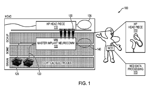
100251 FIG. 1 shows a conceptual view of a transcutaneous
optical communication
system.
100261 FIG. 2 illustrates a block diagram of a first
embodiment of a transcutaneous
optical communication system.
100271 FIGs. 3A-3B illustrate an optical beam shape after
going through optical
phantoms in an experimental configuration.
CA 03151449 2022-3-16
WO 2021/074866 PCT/11112020/059735
100281 FIGs. 4A-4D show several example arrangements for
an optical element.
100291 FIGs. 5A-58 show example arrangements of an
optical element in which four
emitting sources are employed.
100301 FIGs. 6 and 7 show example arrangements of an
impactor in relation to example
optical windows.
100311 FIGs. 8A-8B illustrate in more detail an example
multiple window and ferrule
arrangement.
100321 FIG. 9 illustrates a block diagram of a second
embodiment of a transcutaneous
optical communication system.
DETAILED DESCRIPTION
100331 A description of example embodiments follows.
100341 FIG. 1 illustrates a conceptual view of a
transcutaneous communication system
100. The system 100 includes a master implant neuro-communicator (MIN) 105, an
external
head piece (HP) or wearable device 110, and a data processing device (NCD)
115. As shown
conceptually, the MIN 105 is implanted under a patient's scalp and has signal
wires 120
coupled to cortical electrodes 125 in contact with a portion of the patient's
brain cortex. The
MIN 105 converts physiological signals received on the signal wires 120 to an
optical signal
130 that is transmitted to the HP 110 through the scalp. The HP 110 receives
the optical
signal on the other side of the scalp and converts the received optical signal
into an electric
signal. The electrical signal is amplified by one or more amplifiers, which
feed a clock and
data recovery stage to produce a reconstructed data signal. The NCD 115 is
configured for
data processing functions on the reconstructed data signal. The HP 110 is
configured to
power and control the MIN 105 via coils 135, 140.
100351 FIG. 2 illustrates a block diagram of a first
example embodiment of a
transcutaneous communication system 200. The system 200 includes an
implantable device
or a master implant neuro-communicator (MIN) 205 and an external wearable
device 210.
The MIN 205 has a hermetic housing (not shown) that includes an analog-to-
digital converter
(ADC) 220, a programmable digital signal processor (DSP) 225, one or more
drivers 230,
plural light emitting sources 235, and an integrated optical element 240 that
includes plural
windows. Electrodes 215 provide analog physiological signals to the ADC 220
when attached
to a patient's cortical region 282. It should be understood that other regions
of the body can
CA 03151449 2022-3-16
WO 2021/074866 PCT/11112020/059735
6
also be contemplated for use with embodiments configured based on functions
and elements
of the MIN 205.
100361 The MIN 205 may further include sensors 255,
memory 265, a controller 270 for
configuring the MIN 205, a wireless power receiver 275 for powering the MIN
205, battery
280, and an induction coil 295.
100371 The sensors 255 may include temperature sensors,
humidity sensors, voltage and
current sensors, accelerometers, etc. The sensors 255 are useful for
monitoring the MIN 205
and to ensure safety.
100381 The memory 265 may be arranged to store the
implant's configurations, firmware,
implant and/or patient information (e.g., name, serial number) and/or to log
data (e.g., battery
voltage, temperature, humidity, time, events).
100391 The controller 270 may be a programmable
microcontroller arranged to configure
acquisition, the DSP 225, and the drivers. In addition, the controller 270 may
be configured
to read the sensors 255, to write/read the memory 265, to manage the
communication with
the wearable 210, and to upgrade the implant's firmware.
100401 The wireless power receiver 275 is configured to
convert AC voltage from
induction coil 295 into rectified and regulated clean voltages (DC) to power
the implant's
electronics.
100411 The battery 280 in some embodiments can store
energy to be used during power
interruption, or to power the MIN 205 when the wearable 210 is absent to keep
some
functions running.
100421 The induction coil 295 is configured to convert an
alternating magnetic field into
an alternating electrical signal.
100431 The wearable device 210 includes one or more
photodiodes 245, one or more
amplifier stages 250, and clock and data recovery circuitry 260.
100441 The wearable device 210 further includes an
induction coil 287, a wireless power
emitter 289, and a controller 291.
100451 In operation, the ADC 220 converts the analog
physiological signal received from
electrodes 215 to a digital signal. The ADC function may be provided by, for
example, an
analog front end (AFE) chip. The DSP 225 processes the digital signal. The DSP
225 controls
the ADC 220, reads the result of the analog-to-digital conversions,
encapsulates the data with
a header and a checksum to ensure data integrity and sends the data to one or
more drivers
230. The output of the DSP 225 is coupled to the one or more drivers 230 which
convert the
CA 03151449 2022-3-16
WO 2021/074866 PCT/11112020/059735
7
digital signal to one more modulation signals to drive the plural light
emitting sources 235.
The light beams emitted from the emitting sources 235 contribute to form a
single optical
signal. The integrated optical element 240 has multiple robust low profile
optical windows
that allow the optical signal to exit the hermetic housing and to be safely
injected into the
biological tissue 207. At the wearable device 210, one or more photodiodes 245
receive the
optical signal on the other side of the tissue and convert the received
optical signal into an
electric signal. In alternative embodiments, other types of optical receivers
are used in place
of the photodiodes 245. The electrical signal is amplified by one or more
amplifiers 250,
which feed a clock and data recovery or reconstruction stage 260. The
reconstructed data
signal exits 262 the wearable device 210 for further processing.
100461 The wearable device 210 may be configured to
transfer power from wireless
power emitter 289 to the wireless power receiver 275 at MEN 205 via the
induction coils 287,
295. In addition, the wearable device 210 may be configured to program and
communicate
with the controller 270 at MIN 205 from controller 291 via the induction coils
287, 295.
100471 Target Data Rate
100481 New applications of implantable devices require
large amounts of information to
transit across the patient's tissue, which can typically occur at a date
transfer rate of more
than 25 Mbps, given the number of channels, sampling rate, and resolution
required.
100491 Skin Thickness
100501 The optical power that needs to be transmitted
through tissue is affected by tissue
thickness and type. In an example of potential application of device implanted
in a patient's
head, the tissue thickness can be typically 7 to 8 mm in average, reaching up
to 12 mm, or
even more.
100511 Wavelengths
100521 The skin absorption and scattering coefficients
are not constant and vary with the
wavelength. The ability of light to penetrate biological tissues depends also
on tissue
components such as pigments, melanin, fat, water, and oxy/deoxy blood.
Therefore, the
wavelength is chosen to be able to maximize the transmitted energy, but the
link is also
configured to be flexible and tolerant enough to accommodate all skin
variations.
100531 Many publications identified a "near-infrared
window" in biological tissues,
between 600nm and 1300nm. At these wavelengths, the combination of the
melanin, the
water, and the blood absorbes less light than at shorter or longer
wavelengths. Plus, the
CA 03151449 2022-3-16
WO 2021/074866 PCT/11112020/059735
8
scattering coefficient of biological tissues decreases when the wavelength
increases. In some
embodiments, the wavelength may be in the range between 400nm and 1400nm.
100541 Emitting Source
100551 The optical communication link, unidirectional, is
based on multiple fast emitting
infrared sources, for power adjustment and redundancy (and to decrease the
power density by
spreading the power over the multiple sources), modulated by the digital data
with the
operation of a driver. The scalp thickness, absorption, and scattering
properties can be
compensated by an adjustable emitting source and an adjustable receiver
sensitivity.
Therefore, it is possible to optimize the bit error rate while keeping the
power consumption as
low as possible.
100561 The emitting sources 235 can be light emitting
diodes (LEDs) or vertical-cavity
surface-emitting lasers (VCSELs). Both are types of emitting sources that can
emit infrared
radiations in a small form factor. While LEDs are typically limited to 20Mbps,
VCSELs can
achieve a data rate up to several Gbps.
100571 Driver
100581 In an embodiment, the driver(s) 230 may be a very
simple and high-speed
transistor used to modulate the VCSEL current with a power efficient and
simple On Off
Keying (00K) modulation. The multiple emitting sources can also be operated
using
multiple amplitude shift keying (M-ASK).
100591 Wearable photodiode
100601 The photodiode 245 may be, for example, a
Hamamatsu S6967 photodiode, which
has a 50MHz bandwidth, a sensitivity of about 0.62 W/A at 850nm, a
photosensitive area of
26.4 MM2, and a large viewing angle of more than 1200. Placing the photodiode
245 as close
as possible to the skin has the advantage of providing a large viewing angle,
which also aids
with alignment to the emitting sources. The goal is to be able to capture all
the diffused light
reaching the surface of the skin, even if the photons arrive with a
significant incident angle.
An optical system (e.g., Fresnel lens, lens, filter) (not shown) may be added
to the photodiode
to capture more photons or to select only the wavelength of interest.
100611 Amplifier stages
100621 The photodiode 245 delivers a current proportional
to the optical power received.
The amplifier stage(s) 250 transform this current into a voltage.
100631 In an experimental configuration to demonstrate
the concepts of the implantable
devices described herein, solid optical phantoms have been used to mimic the
optical
CA 03151449 2022-3-16
WO 2021/074866 PCT/11112020/059735
9
properties of the tissue. Nominal and extreme cases for optical properties and
tissue
thickness (2mm and 15mm representing the extremes for skin thickness) have
been used.
100641 FIGs. 3A-38 illustrate the shape of the beam after
going through optical phantoms
in the experimental configuration. FIG. 3A shows results for an optical
phantom A2, which is
2mm thick, and FIG. 3B shows results for an optical phantom A5.5, which is
5.5mm thick.
For the A2 phantom, distinct optical beams from four emitter sources can be
seen separated.
For phantoms thicker than 2mm, such as the A5.5 phantom, the beams are
intersecting and
summed to form a single peak, as shown by FIG. 3B, thanks to the scattering
effect.
Therefore, for thin skin the multiple sources concept increases the alignment
tolerance, and
for thick skins the total beam formed is a combination of the four beams, and
the alignment
tolerance is probably larger due to the scattering coefficient.
100651 It has been found that, in order to accommodate
ranges of thickness of the
biological tissue 207 (FIG. 2), the emitting sources are separated such that
the light beams
that exit the hermetic housing are distributed in a pattern in which a peak
position of light
intensity of each light beam is separated from a corresponding peak position
of light intensity
of an adjacent light beam by at least a first distance and less than a second
distance. For
example, the first distance may be greater than 0.5 mm, and the second
distance may be less
than 50 mm.
100661 The integrated optical element 240 can be, for
example, constructed from sapphire
or other suitable material. FIGs. 4A-4D show several example arrangements for
the optical
element 240. In FIG. 4A the optical element includes a lens 402 such as a
plano-concave
lens. In FIG. 4B an anti-reflective coating 404 (e.g., thin film or thick
film) is applied to a
surface of the optical element 240 to reduce reflection and therefore increase
the transmitted
energy. In FIG. 4C a diffusing layer 406, such as a frosted surface, is
applied to a surface of
the optical element 240. In FIG. 4D the optical element 240 includes a micro-
structured or
micro-patterned surface 408.
100671 FIGs. 5A-5B show two example wangements of the
optical element 240 in which
four emitting sources 235a-235d are employed. In FIG. 5A the optical element
comprises a
single window 502 held in place by a ferrule 504 having a single opening 509a.
In FIG. 5B
the optical element comprises four windows 506a-506d held in place by a
ferrule 508 having
four corresponding openings 510a-510d. Each one of the multiple optical
windows 506a-
506d, covering a subset of infrared emitting sources 235a-235d, can have a
smaller diameter
than a single window covering all sources. For a given thickness, multiple
windows have a
CA 03151449 2022-3-16
WO 2021/074866
PCT/1112020/059735
lower diameter-to-thickness ratio than a single larger window, therefore being
more
mechanically robust. Similarly, with a given recess distance from the surface
of the windows
to the surface of their supporting ferrule, an impactor having a given concave
surface can
directly hit the surface of the larger single window, while avoiding the
surface of the smaller
ones. Put another way, for a given impactor with a given concave surface, the
surface of the
larger single window needs to be recessed further than the surface of the
smaller windows to
avoid an impact. This concept is shown in FIGs. 6 and 7, which show an
impactor 602 having
radius 25mm. In FIG. 6, the large window 502 having a 6.85mm diameter is
recessed by
0.236mm By contrast, in FIG. 7 the small window 506 having a 1.80mm diameter
only
needs to be recessed by 0.016mm to avoid the impactor 602. An advantage of the
smaller
window 506 is that the packaging of the implantable device can be made smaller
since the
recess is smaller.
100681 The combination of a direct impact and a high
diameter-to-thickness ratio
generates an increased probability of damage to the window, possibly resulting
in a loss of
hermeticity: recess distance and/or window thickness would need to be
increased to avoid
that, and both these options would hinder the "low profile" aspect.
100691 FIGs. 8A-8B illustrate in more detail an example
multiple window and ferrule
arrangement. FIG. 8A is a plan view that shows ferrule 805 holding four
sapphire windows
810. The ferrule 805 may be made from titanium or other suitable material. The
centers of the
windows 810 are separated by a distance 830. As shown in the cross-sectional
view (FIG.
8B) through a cutting plane A-A illustrated by lines A-A, the windows 810 are
recessed from
the top 835 of the ferrule by a distance 885. In this embodiment, the windows
810 are not
recessed from the bottom 825 of the ferrule, but in other embodiments, the
windows may be
recessed from bottom also. The ferrule is bonded to each window 810 by a
hermetic seal 820,
by means of a pure gold brazing for example, and includes a flange 840 for
seating the ferrule
in the housing. The distance 830 between centers of windows 810 is selected to
correspond
with placement of the one or more emitting sources 235 (FIG. 2) for alignment
with the
windows 810.
100701 FIG. 9 illustrates a block diagram of a second
example embodiment of a
transcutaneous optical communication system. In this system 900, optical
communication is
directed from a wearable device 910 to an implant device 905. Such a system
900 may be
configured to deliver stimulation signals internally to an area of tissue. In
addition, the system
CA 03151449 2022-3-16
WO 2021/074866
PCT/1112020/059735
11
900 may be configured to provide service signals for programming, upgrading
and/or
changing parameters of the implant device 905.
100711 The implant device 905 has a hermetic housing (not
shown) that includes one or
more photodiodes 945, one or more amplifier stages 950, receiver 960,
controller 978, and
stimulation generator 998. Electrodes 915 provide analog physiological signals
from
stimulation generator 998 when attached to a tissue region of a patient.
100721 The implant device 905 may further include sensors
955, memory 965, a
controller 970 for configuring the implant device 905, a wireless power
receiver 975 for
powering the implant device 905, battery 980, and an induction coil 995.
100731 The sensors 955 may include temperature sensors,
humidity sensors, voltage and
current sensors, accelerometers, etc. The sensors 955 are useful for
monitoring the implant
device 905 and to ensure safety.
100741 The memory 965 may be arranged to store the
implant's configurations, firmware,
implant and/or patient information (e.g., name, serial number) and/or to log
data (e.g., battery
voltage, temperature, humidity, time, events).
100751 The controller 970 may be a microcontroller
arranged to configure controller 978.
In addition, the controller 970 may be configured to read the sensors 955, to
write/read the
memory 965, to manage the communication with the wearable 910 and to upgrade
the
implant's firmware.
100761 The wireless power receiver 975 is configured to
convert AC voltage from
induction coil 995 into rectified and regulated clean voltages (DC) to power
the implant's
electronics.
100771 The battery 980 in some embodiments can store
energy to be used during power
interruption, or to power the implant device 905 when the wearable 910 is
absent to keep
some functions running.
100781 The induction coil 995 is configured to convert an
alternating magnetic field into
an alternating electrical signal.
100791 The wearable device 910 includes one or more
drivers 930, plural light emitting
sources 935, and an integrated optical element 940 that includes plural
windows.
100801 The wearable device 910 further includes an
induction coil 987, a wireless power
emitter 989, and a controller 991.
100811 In operation, the controller 991 provides a
digital signal to the one or more drivers
930 which convert the digital signal to one more modulation signals to drive
the plural light
CA 03151449 2022-3-16
WO 2021/074866
PCT/1112020/059735
12
emitting sources 935. The light beams emitted from the emitting sources 935
contribute to
form a single optical signal. The integrated optical element 940 has multiple
robust low
profile optical windows that allow the optical signal to exit the wearable
device 910 and to be
safely injected into the biological tissue 907. At the implant device 905, one
or more
photodiodes 945 receive the optical signal on the other side of the tissue and
convert the
received optical signal into an electric signal. The electrical signal is
amplified by one or
more amplifiers 950 that feed a receiver 960. The reconstructed data signal is
coupled to
controller 978, which is programmed to control the stimulation generator 998
to provide
stimulation signals to tissue 982.
100821 The wearable device 910 may be configured to
transfer power from wireless
power emitter 989 to the wireless power receiver 975 at implant device 905 via
the induction
coils 987, 995. In addition, the wearable device 910 may be configured to
program the
controller 970 from controller 991 via the induction coils 987, 995.
100831 While example embodiments have been particularly
shown and described, it will
be understood by those skilled in the art that various changes in form and
details may be
made therein without departing from the scope of the embodiments encompassed
by the
appended claims.
CA 03151449 2022-3-16