Note: Descriptions are shown in the official language in which they were submitted.
BEAM DIVERSITY BY SMART ANTENNA WITH PASSIVE ELEMENTS
BACKGROUND
This application is related to PCT Application entitled "Beam Diversity by
Smart
Antenna Without Passive Elements," Attorney Docket Number 86175176PCT01, by
the
same inventors as the present application, filed on herewith date.
The present invention, in some embodiments thereof, relates to an antenna
device, and,
more specifically, but not exclusively, to an antenna device that may be used
with a Wi-Fi
access point.
Wi-Fi is a wireless LAN standard, based on the IEEE standard 802.11, which is
widely
used in home, offices and other indoor / outdoor environments. Wi-Fi operates
in 2
frequency bands, 2.4GHz band and 5GHz band, and manages the communication
between
an Access point and clients (computers, smart handset, various devices, etc.).
The Wi-Fi
protocol was developed to provide service to numerous users at arbitrary
locations of the
Access point' s coverage area. In other words, the Access point needs to cover
the entire
area of its operation. For that reason, a Wi-Fi antenna typically has an
omnidirectional beam
for wide coverage.
The ultimate goal of any Wi-Fi system is to provide the highest possible
throughput for
each user. This goal requires a strong signal, to enable a good Signal to
Interference and
Noise Ratio (SINR). This goal also requires, when necessary, a narrow,
directional beam,
which may be directed with high gain in the direction of a particular user,
while reducing
the interference to other cells. Thus, an ideal Wi-Fi access point should be
able to alternately
emit an omnidirectional beam and to emit a narrow, directional beam.
Various solutions for alternating or diversifying beam coverage in Wi-Fi
antennas are
known. One such solution is based on the use of reflectors and directors. The
principle of
operation of such prior art Wi-Fi antennas is based on the well-known Yagi-Uda
antenna.
A Yagi-Uda antenna is a directional antenna consisting of multiple parallel
elements in a
line, usually half-wave dipoles made of metal rods. Yagi-Uda antennas consist
of a single
driven element connected to the transmitter or receiver with a transmission
line, and
additional parasitic elements which are not connected to the transmitter or
receiver: a
reflector and one or more directors. The reflector and director absorb and re-
radiate the radio
waves from the driven element with a different phase, modifying the dipole's
radiation
1
Date Regue/Date Received 2023-10-03
pattern. The waves from the multiple elements superpose and interfere to
enhance radiation
in a single direction, achieving a very substantial directional increase in
the antenna's gain.
The Yagi-Uda concept has been applied for antenna elements of Wi-Fi Access
points,
to enable the Access point to emit different signal patterns. For example, a
Wi-Fi access
point may consist of a structure with one active element having two vertical
bi-conical
dipoles at the center of the structure, and a very large number of passive
elements arranged
in several circular arrays of different radiuses around it. Each passive
element is made of
several very short metal sections (e.g., shorter than 1/5 of a wavelength)
which may be either
shorted by diodes to one long passive element (around 0.5 wavelength) or left
open.
Shorting the passive elements thus changes them from directors to a reflector,
and thereby
changes the directional gain of the Wi-Fi access points. In another example,
various passive
elements may be arranged in series, with diodes configured therebetween. When
the diodes
are off, the passive elements act as directors. When the diodes are on, the
length of the
passive part is enlarged, and it acts as a reflector.
Another known model for modifying the transmission of Wi-Fi access points
involves
selectively activating one of a plurality of radiating dipoles, each of which
is attached to a
ground component. The selection of the active dipole or dipoles may be done by
operating
series switches, e.g., diodes, on the feeding line of each dipole near its
input. The radiating
dipoles are of different sizes or configurations. Each dipole may be chosen
depending on
the type or characteristics of the signal that is desired.
Another model for diversifying the signal at Wi-Fi access points involves
integrating
both horizontally and vertically polarized elements within a single Wi-Fi
access point. This
model does not alter any signal characteristics, but rather integrates various
signals into a
single Access point.
SUMMARY
The foregoing models for modifying the signals in Wi-Fi antennas all rely on
the
inclusion of additional, space-consuming elements in the antenna system. For
example,
reliance on the Yagi-Uda principle requires inclusion of a large number of
passive devices
to serve as directors and reflectors. Similarly, selection from a plurality of
radiating dipoles
requires inclusion of additional radiating dipoles. In addition, use of both
horizontally and
vertically polarized elements adds one or more radiating dipole into the
access point, and is
2
Date Regue/Date Received 2023-10-03
not useful for a standard Wi-Fi access point, in which there is a single
antenna that is only
horizontally or vertically polarized.
In addition, above-described models, with their various additional passive
elements,
active dipoles, and/or antennas with multiple polarizations, require an access
point with a
larger area or footprint. The excess space is a particularly important
consideration for
enterprise-grade Wi-Fi access points. An enterprise-grade Wi-Fi access point
supports two
or three bands, with 8 or 16 antennas for 5 GHz, and an additional four
antennas for 2.4GHz.
The additional elements required for each of the antennas would thus greatly
enlarge the
size requirements of the antenna device.
Accordingly, there is a need for a smart antenna device that provides the
ability to
alternate radiating beams between omnidirectional coverage and directional
beam coverage.
There is additionally a need for a smart antenna device that can respond to
dynamic changes
in the operational environment, in order to select properly when to utilize
the
omnidirectional beam coverage or the directional beam coverage. In addition,
there is a need
for a smart antenna device that incorporates an antenna which occupies a
minimum of space.
It is therefore an object of the present invention to provide a smart antenna
device
with the ability to alternate radiating beams between omnidirectional coverage
and
directional beam coverage pointing to a specific sector within a coverage
area.
The foregoing and other objects are achieved by the features of the
independent
claims. Further implementation forms are apparent from the dependent claims,
the
description and the figures.
According to a first aspect, an antenna device comprises a plurality of dipole
antennas and a port. Each of the dipole antennas is connected to the port, and
the plurality
of dipole antennas are arranged around the port. Each of the plurality of
dipole antennas
comprises two ends. The antenna device further comprises a plurality of
passive elements.
The ends of the plurality of dipole antennas and the plurality of passive
elements are
interchangeably arranged around the port, such that each of the plurality of
passive elements
is situated between ends of two different antennas from the plurality of
dipole antennas. One
or more switches are configured to switch between an omnidirectional state, in
which the
ends of the dipole antennas are not connected to the plurality of passive
elements, and a
directional state, in which at least one end of one of the plurality of
passive elements is
connected to at least one end of one of the plurality of antennas.
3
Date Regue/Date Received 2023-10-03
An advantage of this aspect is that the antenna device may be switched between
omnidirectional state and the directional state using only passive elements
that are situated
on the perimeter of the array of dipole antennas. This permits mode switching
without
increasing the space requirement of the antenna device. In the omnidirectional
state, when
the dipole antennas are not connected to each other, the antenna device
provides a high gain
pattern in the azimuthal plane. The antenna device is also convertible to a
high gain
directional pattern in the azimuthal plane, when two ends in each of one or
more of the pairs
are connected to each other.
In an implementation of the antenna device according to the first aspect, in
the
directional state, at least two ends of one of the plurality of passive
elements are connected
to two different antennas, thereby converting the two different antennas into
a single long
radiating element having two feeding points. Advantageously, the at least two
combined
dipole antennas thus function as a single long radiating element antenna,
thereby increasing
the directional gain.
In another possible implementation of the antenna device according to the
first
aspect, the plurality of dipole antennas and the plurality of passive elements
are arranged
around the port in a substantially rectangular or substantially circular
orientation.
Advantageously, these exemplary orientations are well suited for providing an
omnidirectional signal.
In another possible implementation of the antenna device according to the
first
aspect, the plurality of dipole antennas are arranged horizontally above a
ground plane. The
ground plane may serve as a reflecting surface for the antenna waves of the
dipole antenna,
to increase the gain of the antenna device, in both the omnidirectional and
directional states.
In another possible implementation of the antenna device according to the
first
aspect, the plurality of dipole antennas comprises at least three dipole
antennas. A minimum
of three dipole antennas is necessary in order to distinguish between the
omnidirectional
state, when none of the antennas are connected to each other, and the
directional state, when
at least two of the antennas are connected to each other and at least one is
not connected.
In another possible embodiment of the antenna device according to the first
aspect,
the gain in the entire azimuth plane is at least 4 dBi. This gain in the
azimuth plane enables
the antenna to be used to transmit a Wi-Fi signal to a suitably large area.
4
Date Regue/Date Received 2023-10-03
In another possible implementation of the antenna device according to the
first
aspect, the difference in gain between the omnidirectional state and the
directional state is
at least 3 dB. Advantageously, the difference in gain in the desired direction
in the
directional state, as compared to the gain in that direction in the
omnidirectional state, is
suitably significant.
In another possible implementation of the antenna device according to the
first
aspect, the antenna device further comprises electronic circuitry for
connecting and
disconnecting each passive element and adjacent antenna, and a control
algorithm for
determining which passive element to connect to an adjacent antenna, in order
to steer an
antenna beam of the antenna device in a directional state towards a location
of one or more
mobile devices. In this implementation, the antenna device is thus part of a
smart antenna
that may be toggled back and forth between the omnidirectional and directional
states
according to the needs of the environment, e.g., the location of mobile
devices within a
given range of the antenna device.
In another possible implementation of the antenna device according to the
first
aspect, the one or more switches comprise at least one of a diode, a
transistor, and an
electronic switch. The switches may be integrated with the control algorithm
for toggling
the smart antenna between the omnidirectional and directional states.
In a second aspect of the invention, a method for switching an antenna device
from
an omnidirectional state to a directional state is disclosed. The antenna
device comprises a
plurality of dipole antennas and a port. Each of the dipole antennas is
connected to the port.
The plurality of dipole antennas are arranged around the port. Each of the
plurality of dipole
antennas comprises two ends. The antenna device further comprises a plurality
of passive
elements interchangeably arranged around the port such that each of the
plurality of passive
elements is situated between two different antennas from the plurality of
dipole antennas.
The antenna device further comprises one or more switches configured to switch
between
(1) an omnidirectional state, in which the ends of the dipole antennas are not
connected to
the plurality of passive elements; and (2) a directional state, in which at
least one of the
plurality of passive elements is connected to at least one end of one of the
plurality of dipole
antennas. The method comprises operating the one or more switches to connect
at least one
end of the at least one of the plurality of passive elements to at least one
end of the plurality
5
Date Regue/Date Received 2023-10-03
of dipole antennas, and thereby switching the antenna device from the
omnidirectional state
to the directional state.
An advantage of this aspect is that the method may be used to switch the
antenna
device between the omnidirectional state and the directional state using only
passive
elements that are situated on the perimeter of the array of dipole antennas.
This permits
mode switching without increasing the space requirement of the antenna device.
In the
omnidirectional state, when the dipole antennas are not connected to each
other, the antenna
device provides a high gain pattern in the azimuthal plane. The antenna device
is also
convertible to a high gain directional pattern in the azimuthal plane, when
two ends in each
of one or more of the pairs are connected to each other.
In an implementation of the method according to the second aspect, the method
comprises connecting at least one of the plurality of passive elements to two
different
antennas, thereby converting the two different antennas into a single long
radiating element
having two feeding points. Advantageously, in the directional state, the at
least two
combined dipole antennas thus function as a single long radiating element
antenna.
In an implementation of the method according to the second aspect, the method
further comprises increasing the gain between the omnidirectional state and
the directional
state in at least one direction by at least 3 dB. Advantageously, the
difference in gain in the
desired direction in the directional state, as compared to the gain in that
direction in the
omnidirectional state, is suitably significant.
In an implementation of the method according to the second aspect, the method
further comprises determining which direction to steer an antenna beam of the
antenna
device towards a location of one or more mobile devices. In this
implementation, the
antenna device is part of a smart antenna that may be toggled back and forth
between the
omnidirectional and directional states according to the needs of the
environment, e.g., the
location of mobile devices within a given range of the antenna device.
In a further implementation of the method according to the second aspect, the
method further comprises determining when to revert the antenna device back to
the
omnidirectional state, and operating the one or more switches, and thereby
switching the
antenna device back from the directional state to the omnidirectional state.
In this
implementation, the antenna device is part of a smart antenna that may be
toggled back and
6
Date Regue/Date Received 2023-10-03
forth between the omnidirectional and directional states according to the
needs of the
environment, e.g., the location of mobile devices within a given range of the
antenna device.
Unless otherwise defined, all technical and/or scientific terms used herein
have the
same meaning as commonly understood by one of ordinary skill in the art to
which the
invention pertains. Although methods and materials similar or equivalent to
those described
herein can be used in the practice or testing of embodiments of the invention,
exemplary
methods and/or materials are described below. In case of conflict, the patent
specification,
including definitions, will control. In addition, the materials, methods, and
examples are
illustrative only and are not intended to be necessarily limiting.
BRIEF DESCRIPTION OF THE SEVERAL VIEWS OF THE DRAWINGS
Some embodiments of the invention are herein described, by way of example
only,
with reference to the accompanying drawings. With specific reference now to
the drawings
in detail, it is stressed that the particulars shown are by way of example and
for purposes of
illustrative discussion of embodiments of the invention. In this regard, the
description taken
with the drawings makes apparent to those skilled in the art how embodiments
of the
invention may be practiced.
In the drawings:
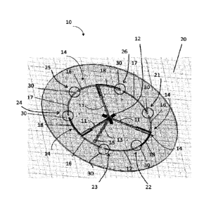
FIG. 1 is a depiction of an antenna device in an omnidirectional state,
according to
some embodiments of the invention;
FIG. 2 is a depiction of the near electric field generated by the antenna
device of
FIG. 1 in the omnidirectional state, according to some embodiments of the
invention;
FIG. 3 is a depiction of the far electric field generated by the antenna
device of
FIG. 1 in the omnidirectional state, taken in the azimuthal plane at 0 = 135,
according to
some embodiments of the invention;
FIGS. 4A and 4B are depictions of the realized gain in total of the antenna
device of
FIG. 1, measured spherically around the antenna device, according to some
embodiments
of the invention;
FIG. 5 is a depiction of the impedance matching of the antenna device of FIG.
1 in
the omnidirectional state, according to some embodiments of the invention;
FIG. 6 is a depiction of the antenna device of FIG. 1 in a directional state,
according
to some embodiments of the invention;
7
Date Regue/Date Received 2023-10-03
FIG. 7 is a depiction of the near electric field generated by the antenna
device of
FIG. 6 in the directional state, according to some embodiments of the
invention;
FIG. 8 is a depiction of the far electric field generated by the antenna
device of FIG.
6 in the directional state, taken in the azimuthal plane at 0 = 135, according
to some
embodiments of the invention;
FIGS. 9A and 9B are depictions of the realized gain in total of the antenna
device of
FIG. 6 in the directional state, measured spherically around the antenna
device, according
to some embodiments of the invention;
FIG. 10 is a depiction of the impedance matching of the antenna device of FIG.
6 in
the directional state, according to some embodiments of the invention; and
FIG. 11 is a depiction of steps of a method of switching an antenna device
from an
omnidirectional state to a directional state, according to some embodiments of
the invention.
DETAILED DESCRIPTION
The present invention, in some embodiments thereof, relates to an antenna
device,
and, more specifically, but not exclusively, to an antenna device that may be
used with a
Wi-Fi access point.
Before explaining at least one embodiment of the invention in detail, it is to
be
understood that the invention is not necessarily limited in its application to
the details of
construction and the arrangement of the components and/or methods set forth in
the
following description and/or illustrated in the drawings and/or the Examples.
The invention
is capable of other embodiments or of being practiced or carried out in
various ways.
Referring to FIG. 1, antenna device 10 comprises a plurality of dipole
antennas 14,
each electrically connected to port 12. The port 12 is electrically connected
via conducting
wire 13 to power source 15. The plurality of dipole antennas 14 may be
arranged on an FR-4
substrate, or on any other suitable substrate, such as a printed circuit
board. The plurality
of dipole antennas are arranged horizontally above a ground plane 20. Ground
plane 20 is a
flat or nearly flat horizontal conducting surface extending underneath the
dipole
antennas 14. For purposes of clarity, ground plane 20 may extend further
outwards in all
directions, and may have any suitable dimension. The ground plane may serve as
a
reflecting surface for the antenna waves of the dipole antennas 14, to
increase the gain of
the antenna device 10.
8
Date Regue/Date Received 2023-10-03
In the illustrated embodiment, there are three dipole antennas 14. The choice
of three
dipole antennas 14 is merely exemplary, and there may be fewer or more dipole
antennas 14.
In a preferred embodiment, there are at least three dipole antennas 14. Each
dipole
antenna 14 is configured asymmetrically, with a feeding arm 11 connecting to
the port 12,
and arms 16 and 18. In the depicted embodiment, arms 16 and 18 are
approximately equal
in length. However, arms 16 and 18 may also be asymmetrical. The dipole
antenna 14 may
have a total length that is half of the wavelength of the transmitted signal.
Thus, for
example, for a signal transmitted at 5 GHz, the wavelength is 60 mm in free
space and about
30 mm on the FR4 substrate, and the total length of both arms of dipole
antenna 14, printed
on the FR4 substrate, is about 15 mm.
The dipole antennas 14 are configured around the port 12 in a closed shape. In
the
illustrated embodiment, the closed shape is a circle; however, the closed
shape may also be
a rectangle, or any other polygon.
Passive elements 17 are configured between arms 16, 18 of the antennas.
Passive
elements 17 are metal strips. The passive elements 17 are configured on the
perimeter of a
circular or polygonal array around port 12. The length of each passive element
is also
approximately half of the transmitted wavelength, e.g., 15 mm for a 5 GHz
signal.
Passive elements 17 are configured adjacent to arms 16, 18 of dipole antenna
14.
The passive elements 17 and the arms 16, 18 define junction points around the
perimeter of
the antenna array. In the illustrated embodiment, in which there are three
antennas 14, there
are six junction points, 21,22, 23, 24, 25, and 26. The ends of arms 16, 18
are either above
the corresponding passive element 17 or in the same plane almost touching the
passive
element 17.
A switch 30 is arranged at each of the junction points 21-26. The switch 30
comprises electronic circuitry for connecting and disconnecting the passive
elements 17 and
the adjacent arms 16, 18 of the dipole antennas 14. This electronic circuitry
may be, for
example, a diode, a transistor, and/or an electronic switch. The switch 30 is
switchable
between an "on" position, in which the electronic circuitry forms a closed, or
shorted, circuit
between the adjacent passive elements 17 and anus 16, 18, and an "off'
position, in which
the passive elements 17 and arms 16, 18 remain unconnected. In the embodiment
of FIG. 1,
each switch 30 is depicted as an open circle, indicating that it is in the
"off' position. The
switches 30 may be connected to a remote processor (not shown) with a control
algorithm
9
Date Regue/Date Received 2023-10-03
for determining whether to operate switch 30 at each of the junction points 21-
26. The
remote processor and control algorithm may be used to toggle the antenna
device 10 back
and forth between the omnidirectional state and a directional state, as will
be discussed
further herein.
In the embodiment of FIG. 1, because each switch 30 is in the "off" position,
the
antenna device 10 has an identical configuration throughout the entire
circumference of
antenna device 10. For this reason, antenna device 10 generates an
omnidirectional electric
field, as will be discussed in connection with FIGS. 2-4, and is said to be in
an
omnidirectional state.
FIG. 2 depicts an electric field that is generated along each dipole antenna
14, when
the antenna device 10 is in the omnidirectional state. The strength of the
electric field is
measured in Volts per meter (V/m). For purposes of illustration, the strength
of the electric
field is divided into five regions. It is to be recognized that the variations
in electric field
across antenna device 10 are continuous, rather than discrete, and the
following
approximations of electric field for each particular region are for purposes
of general
explanation only. In region 42, both on feeding arms 11 and on the perimeter
of antenna
device 10 (both the region of arms 16, 18 and the passive elements 17, which
is unconnected
to the rest of antenna device 10) the electric field is between 100 and 1,680
V/m. In region
43, both on feeding arms 11 and on the perimeter of antenna device 10, the
electric field is
between 1,680 and 3,787 V/m. In region 44, both on feeding arm 11 and on the
perimeter
of the antenna device 10, the electric field is between 3,787 and 5,893 V/m.
In region 45,
both on feeding arm 11 and on the perimeter of antenna device 10, the electric
field is
between 5,893-6,947 V/m. Finally, at region 46, corresponding to the portion
of the dipole
antennas 14 closest to port 12, and also at a small portion of the antenna
arms 16, the electric
field is between 6,947 and 8,000 V/m. As can be seen, the electric field is
symmetrical
around the perimeter of antennas 14, and there is no meaningful distinction in
the electric
field at corners 32, 34, 36, and 38 of antenna device 10.
FIG. 3 depicts the far electric field generated by antenna device 10 in the
omnidirectional state. Far electric field 48 is measured in dBi as the
azimuthal plane pattern,
at frequency of 5.5 GHz, with theta at 135. As can be seen, far electric field
48 is measured
at more than 4 dBi, and nearly 6 dBi, throughout the circumference of the
azimuthal plane.
The reason that the far electric field 48 has an omnidirectional profile is
because the near
Date Regue/Date Received 2023-10-03
electric field shown in FIG. 2 has circular symmetry. As a result, far field
48 has a low
ripple omnidirectional pattern.
FIGS. 4A and 4B depict the gain 50 generated by the antenna device 10 in the
omnidirectional state. FIG. 4A illustrates the shape of the gain 50 profile in
three
dimensions, and FIG. 4B depicts the values of the gain 50 for various regions
in the 3
dimensional profile, expressed in dBi. As can be seen in FIGS. 4A and 4B, in
the
omnidirectional state, the gain 50 can be measured along an approximately
ellipsoidal plot.
In addition, as seen best in FIG. 4A, the gain is approximately equivalent at
each point along
the azimuthal plane (i.e., a cross section taken along the X-Y planes). As
seen in FIG. 4B,
the realized gain in region 51 is -23.911 to -14.342 dBi; in region 52, the
realized gain is
between -14.432 and -4.7726 dBi; in region 53, the realized gain is between -
4.7226 dBi
and 1.1967 dBi; in region 54, the realized gain is between 1.1967 to 2.4042
dBi; in region
55, which is the largest region, the realized gain is between 2.2042 dBi and
4.7965 dBi; and
in region 56, the realized gain is around 4.7965 dBi. The differences in gain
across the 3-
dimensional profile are continuous, rather than discrete, and the regions 51-
56 are drawn
for purposes of general illustration only. FIGS. 4A and 4B demonstrate that
the antenna
device 10 may generate a gain of at least 4 dBi in 3 dimensions.
FIG. 5 depicts the impedance matching of the antenna device 10 in the
omnidirectional state. In electronics, impedance matching is the practice of
designing the
input impedance of an electrical load or the output impedance of its
corresponding signal
source to maximize the power transfer or minimize signal reflection from the
load. In FIG.
5, the matching is illustrated for Sll at a frequency range of 5.15 to 5.85
GHz. As is known
to those of skill in the art, Sll is a measure of antenna efficiency that
represents how much
power is reflected from the antenna. This measure is known as the reflection
coefficient or
the return loss. For example, if Sll is 0 dBi, then all the power is reflected
from the antenna,
and none is radiated. If Si! is less than 0 dBi, it is an indication that a
portion of the power
is radiated from the antenna. The more that Sll is negative, the less the
amount of power
that is reflected from the antenna, and the more power is radiated from the
antenna.
As seen in FIG. 5, at 5.150 GHz, the return loss, or matching (indicated on
the Y-
axis) is -10.3382 decibels; at 5.500 GHz, the matching is -14.3404 decibels,
and at 5.850
GHz, the matching is -28.7257 decibels. Thus, each dipole antenna 14 transmits
effectively
11
Date Regue/Date Received 2023-10-03
at all frequencies between 5.150 and 5.850 GHz, and, from the measured range,
transmits
most effectively (i.e., absorbs the least amount of power, and radiates best)
at 5.850 GHz.
Attention is now directed to FIGS. 6-10, which illustrate the antenna device
10 in a
directional state. FIG. 6 illustrates the antenna device 10, which is
identical to the antenna
device 10 as depicted in FIG. 1, with the following exception: whereas in FIG.
1, each of
the switches 30 associated with junction points 21-26 was "off," in FIG. 6,
the switch 30
associated with junction points 22 and 23 are "on," and thus depicted as a
filled circle, while
the other switches 30 are off, and thus depicted as an open circle.
The effect of turning on the switches 30 at junction points 22 and 23 is to
combine
two adjacent dipole antennas 14 into a single long radiating element, or
dipole antenna, 19
having two feeding points. The combined dipole antenna 19 thus extends from
junction
point 21, through junction points 22 and 23, which is now closed, including
passive element
17 which is between junction points 22 and 23, and to junction point 24. The
other dipole
antenna 14 and passive elements 17 remain as they were originally. The two
combined
dipole antennas 14 and passive element 17 thus function as a single dipole
antenna. The
result of combining the two dipole antennas 14 is to change the current
distribution on these
dipole antennas. Specifically, the energy in the combined dipole antenna 19 is
lower
compared to the energy in the separate dipole antennas 14. This increases the
directional
gain in the direction directly opposite the combined dipole antenna 19,
relative to the
directions in which the dipole antennas 14 are combined.
Notably, the use of switches 30 enables the antenna device 10 to be switched
between a directional state and an omnidirectional state using only passive
elements 17 that
are situated on the perimeter of the array of dipole antennas. This permits
mode switching
without increasing the space requirement of the antenna device 10. The mode
switching is
based on using the passive elements 17 to couple multiple dipole antennas 14
to each other.
FIG. 7 depicts an electric field that is generated along each dipole antenna
14 and
the combined dipole antenna 19, when the antenna device 10 is in the
directional state. The
strength of the electric field is measured in Volts per meter (V/m). The
strength of the
electric field is divided into the same five regions 42, 43, 44, 45, 46 as in
FIG. 2. As
described above in connection with FIG. 2, it is to be recognized that the
variations in
electric field across antenna device 10 are continuous, rather than discrete,
and the
12
Date Regue/Date Received 2023-10-03
approximations of electric field for each particular region are for purposes
of general
explanation only.
As can be seen in FIG. 7, and in contrast to the electric field of FIG. 2, in
the
directional mode, the electric field is not symmetric around the entire
antenna device 10.
For example, the maximum energy achieved in passive elements 17 that are not
part of
combined dipole antenna 19 is in the highest energy region 46. Such high
energy regions
are located, for example, at junction points 21, 24, 25, and 26. However, no
such high
energy region 46 exists at closed junction points 22,23.
FIG. 8 depicts the far electric field generated by antenna device 10 in the
directional
state. Far electric field 60 is measured in dBi as the azimuthal plane
pattern, at frequency of
5.5 GHz, with theta at 135. As can be seen, far electric field 60 exceeds 6
dBi between the
angles of 30' and 15a. At angles lower than 30' and higher than 15Cf, the
electric field 60 is
lower than 6 dBi, and, between -90" and -150', it descends to below 0 dBi. The
reason that
the far electric field 60 has a non-symmetrical profile is because of the
asymmetry in the
near electric field shown in FIG. 7. The asymmetrical near electric field over
the dipoles
produces strong directivity in the far electric field, in the direction
opposite combined
antenna 19.
FIGS. 9A and 9B depict the gain 62 generated by the antenna device in the
directional state. FIG. 9A illustrates the shape of the gain 62 profile in
three dimensions,
and FIG. 9B depicts the values of the gain 62 for various regions in the 3
dimensional
profile, expressed in dBi. As can be seen in FIGS. 9A and 9B, in the
directional state, areas
of high gain 64, 66 assume an approximately hemispherical profile. The areas
of low gain,
such as areas 72 and 74, assume a more limited profile, and approximately
correspond to
the low gain area of the far electric field as depicted in FIG. 8.
As seen in FIG. 9B, the realized gain is strongly directional. In region 64,
the
realized gain is around 8.0800 dBi; in region 66, the realized gain is 4.9408
to 8.0800 dBi;
in region 68, the realized gain is -1.3388 to 4.9404 dBi; in region 70 the
realized gain is -
4.4783 to -1.3388 dBi; in region 72 the realized gain is -7.8179 dBi to -
4.4783 dBi; and in
region 74 the realized gain is -20.176 to -7.8179 dBi.
As can be seen from a comparison of the realized gain in FIGS. 8, 9A and 9B
versus
FIGS. 3, 4A and 4B, the maximum gain in the directional state is more than 3dB
greater
than the maximum gain in the omnidirectional state. For example, the maximum
gain in
13
Date Regue/Date Received 2023-10-03
region 64 of FIG. 9B is 8.0800 dBi, whereas the maximum gain in region 56 of
FIG. 4B is
4.7695 dBi. Thus, the directional state provides a significantly higher gain
in the desired
direction, compared to the gain in that direction in the omnidirectional
state.
FIG. 10 depicts the impedance matching of the antenna device 10 in the
directional
state. In FIG. 10, the matching is illustrated for Sll at a frequency of
around 5.50 GHz. As
seen in FIG. 10, at 5.150 GHz, the matching (indicated on the Y-axis) is -
11.6898 decibels;
at 5.500 GHz, the matching is -16.4896 decibels, and at 5.850 GHz, the
matching is -
14.9166 decibels.
A comparison of FIG. 10 and FIG. 5 shows that, in both the omnidirectional and
directional states, there is a wide band of frequencies with matching below -
10 decibels.
Specifically, the matching is below -10 decibels across the entire range of
5.150 to 5.850
GHz.
The presence of passive elements 17 plays an important role in enabling the
above-
described wide band matching. One of the main problems in design of smart
antennas is
matching. In the described embodiment, there is an array of three dipole
antennas 14 on a
single feeding network. Usually, with careful design of dipoles and their
feeding network,
one can get good matching for a single state, e.g., the omnidirectional state
of the depicted
embodiment. But, in the depicted embodiment, it is necessary to design a
single feeding
network that provides good matching in two states, omnidirectional and
directional. With
careful design of the passive elements 17, i.e., with specific calculation of
their length and
width (e.g., a length that is half the transmitted wavelength), it is possible
to achieve wide
matching in both the omnidirectional and directional mode (based on the
principle that two
dipole antennas 14 and one passive element 17 turn into a single radiating
element 19 with
two excitations).
The described antenna device 10 has many other benefits compared to
alternative
devices. The structure of antenna device 10 has a small form-factor, which
enables it to be
included in a small size access point. Furthermore, the ability to achieve
high gain in the
omnidirectional mode enables achieving low error vector magnitude (EVM) with
relatively
high transmission power (high effective isotropic radiation power (EIRP)).
Furthermore,
the unique mechanism of the beam diversion in directional mode provides high
additional
gain. The antenna device 10 may be manufactured very simply, e.g., as a PCB
trace antenna,
and thus is cost-effective.
14
Date Regue/Date Received 2023-10-03
FIG. 11 depicts steps of a method 100 of switching an antenna device 10 from
an
omnidirectional state to a directional state, according to some embodiments of
the invention.
Antenna device 10 comprises a plurality of dipole antennas 14 and a common
port 12. Each
of the dipole antennas 14 is connected to the common port 12. The plurality of
dipole
antennas 14 are arranged around the port 12. Each of the plurality of dipole
antennas 14
comprises two ends 16, 18. The antenna device further comprises a plurality of
passive
elements 17 interchangeably arranged around the port 12 such that each of the
plurality of
passive elements 17 is situated between two different antennas 14 from the
plurality of
dipole antennas 14. The antenna device 10 further comprises one or more
switches 30
configured to switch between (1) an omnidirectional state, in which the ends
16, 18 of the
dipole antennas 14 are not connected to the plurality of passive elements 17;
and (2) a
directional state, in which at least one of the plurality of passive elements
17 is connected
to at least one end 16, 18 of one of the plurality of dipole antennas 14.
The method commences when antenna device 10 is in the omnidirectional state,
which may be a default state. At step 101, the device 10 optionally determines
a desired
direction of field for the directional state. This determination may be based
on the detection
of one or more mobile devices in the vicinity of antenna device 10, e.g., when
the one or
more mobile devices are clustered in a particular direction relative to the
antenna device 10.
The antenna device may be part of a smart antenna that may be toggled back and
forth
between the omnidirectional and directional states according to the needs of
the
environment, e.g., the sensing of mobile devices within a given range of the
antenna device.
At step 102, one or more switchinges 30 are operated, to switch antenna device
10
from the omnidirectional state to the directional state, so that the device 10
will generate a
directional field in the desired direction. The operating step 102 comprises
switching the
antenna device 10 from an omnidirectional state, in which none of the ends of
passive
elements 17 and dipole antennas 14 connect to each other, to a directional
state, in which at
least one end of at least one of the passive elements 17 is connected to at
least one end of
one of the dipole antennas 14. More specifically, the operating step 102
comprises operating
the one or more switches 30 to connect an adjacent passive element 17 and
dipole
antennas 14.
Advantageously, the method may be used to switch the antenna device between
the
omnidirectional state and the directional state using only passive elements
that are situated
Date Regue/Date Received 2023-10-03
on the perimeter of the array of dipole antennas. This permits mode switching
without
increasing the space requirement of the antenna device. In the omnidirectional
state, when
the dipole antennas are not connected to each other, the antenna device
provides a high gain
pattern in the azimuthal plane. The antenna device is also convertible to a
high gain
directional pattern in the azimuthal plane, when two ends in each of one or
more of the pairs
are connected to each other.
At step 103, the method further comprises determining when to revert the
antenna
device back to the omnidirectional state. This determination may be based on
the detection
of one or more mobile devices in the vicinity of antenna device 10, e.g., at
numerous
directions around the antenna device 10. At step 104, the method further
comprises
operating the one or more switches 30, and thereby switching the antenna
device back from
the directional state to the omnidirectional state. In this implementation,
the antenna device
10 is part of a smart antenna that may be toggled back and forth between the
omnidirectional
and directional states according to the needs of the environment, e.g., the
location of mobile
devices within a given range of the antenna device 10.
At step 105, the method is reiterated. That is, upon detection of one or more
devices
in a single direction relative to the antenna device 10, the antenna device 10
may be switched
back to the directional state, in the manner described above.
As can be understood by those of skill in the art, each of the measurements
for the
electric field, gain, and impedance matching of the antenna device 10
discussed above are
for one particular embodiment of the antenna device 10. Adjustments in various
parameters
of the antenna device 10, such as the length of arms 16, 18, the length of
passive
elements 17, the length of feeding arm 11, the orientation of the dipole
antennas 14 and
passive elements 17 around the port 12, the structure of the closed shape
formed by the
dipole antennas 14 and passive elements 17, the size and location of ground
plane 20 relative
to the dipole antennas 14, and the energy delivered from power source 15, all
influence the
electric field, gain, and impedance matching. Accordingly, the values
described above
should be understood in an exemplary, as opposed to a limiting, sense.
The descriptions of the various embodiments of the present invention have been
presented for purposes of illustration, but are not intended to be exhaustive
or limited to the
embodiments disclosed. Many modifications and variations will be apparent to
those of
ordinary skill in the art without departing from the scope and spirit of the
described
16
Date Regue/Date Received 2023-10-03
embodiments. The terminology used herein was chosen to best explain the
principles of the
embodiments, the practical application or technical improvement over
technologies found
in the marketplace, or to enable others of ordinary skill in the art to
understand the
embodiments disclosed herein.
It is expected that during the life of a patent maturing from this application
many
relevant dipole antennas and passive elements will be developed and the scope
of the term
dipole antenna and passive element is intended to include all such new
technologies a priori.
As used herein the tenn "about" refers to 10 %.
The terms "comprises", "comprising", "includes", "including", "having" and
their
conjugates mean "including but not limited to". This telin encompasses the
terms
"consisting of' and "consisting essentially of'.
The phrase "consisting essentially of' means that the composition or method
may
include additional ingredients and/or steps, but only if the additional
ingredients and/or steps
do not materially alter the basic and novel characteristics of the claimed
composition or
method.
As used herein, the singular foul' "a", "an" and "the" include plural
references unless
the context clearly dictates otherwise. For example, the term "a compound" or
"at least one
compound" may include a plurality of compounds, including mixtures thereof.
The word "exemplary" is used herein to mean "serving as an example, instance
or
illustration". Any embodiment described as "exemplary" is not necessarily to
be construed
as preferred or advantageous over other embodiments and/or to exclude the
incorporation
of features from other embodiments.
The word "optionally" is used herein to mean "is provided in some embodiments
and not provided in other embodiments". Any particular embodiment of the
invention may
include a plurality of "optional" features unless such features conflict.
Throughout this application, various embodiments of this invention may be
presented in a range format. It should be understood that the description in
range format is
merely for convenience and brevity and should not be construed as an
inflexible limitation
on the scope of the invention. Accordingly, the description of a range should
be considered
to have specifically disclosed all the possible subranges as well as
individual numerical
values within that range. For example, description of a range such as from 1
to 6 should be
considered to have specifically disclosed subranges such as from 1 to 3, from
1 to 4, from 1
17
Date Regue/Date Received 2023-10-03
to 5, from 2 to 4, from 2 to 6, from 3 to 6 etc., as well as individual
numbers within that
range, for example, 1, 2, 3, 4, 5, and 6. This applies regardless of the
breadth of the range.
Whenever a numerical range is indicated herein, it is meant to include any
cited
numeral (fractional or integral) within the indicated range. The phrases
"ranging/ranges
between" a first indicate number and a second indicate number and
"ranging/ranges from"
a first indicate number "to" a second indicate number are used herein
interchangeably and
are meant to include the first and second indicated numbers and all the
fractional and integral
numerals there between.
It is appreciated that certain features of the invention, which are, for
clarity,
described in the context of separate embodiments, may also be provided in
combination in
a single embodiment. Conversely, various features of the invention, which are,
for brevity,
described in the context of a single embodiment, may also be provided
separately or in any
suitable subcombination or as suitable in any other described embodiment of
the invention.
Certain features described in the context of various embodiments are not to be
considered
essential features of those embodiments, unless the embodiment is inoperative
without those
elements.
Although the invention has been described in conjunction with specific
embodiments thereof, it is evident that many alternatives, modifications and
variations will
be apparent to those skilled in the art. Accordingly, it is intended to
embrace all such
alternatives, modifications and variations that fall within the spirit and
broad scope of the
appended claims.
Citation or identification of any reference in this application shall not be
construed
as an admission that such reference is available as prior art to the present
invention. To the
extent that section headings are used, they should not be construed as
necessarily limiting.
18
Date Regue/Date Received 2023-10-03