Note: Descriptions are shown in the official language in which they were submitted.
CA 03154668 2022-03-15
WO 2021/046635
PCT/CA2020/051188
GNSS ANTENNA SYSTEMS, ELEMENTS AND METHODS
CROSS-REFERENCE TO RELATED APPLICATIONS
[001] This patent application claims the benefit of priority from U.S.
Provisional Patent
Application 62/900,605 filed September 15, 2019 entitled "GNSS Antenna
Element," the entire
contents of which are incorporated herein by reference.
FIELD OF THE INVENTION
[002] This patent application relates to global navigation satellite systems
and more
particularly to antennas, antenna elements and antenna assemblies employing
one or more pairs
of antenna elements each electromagnetically coupled to a dipole with enhanced
azimuthal
performance and/or wide bandwidth high precision high purity reception.
BACKGROUND OF THE INVENTION
[003] Global satellite navigation systems or global navigation satellite
systems (GNSS)
employ a network of geo-spatially positioned satellites to broadcast precisely
synchronized
navigation messages, thereby providing for determination of a network time and
a geolocation
by dedicated GNSS receivers. Such receivers provide for a ubiquitous and
global time
reference, in addition to a host of geolocation uses, ranging from consumer
navigation devices
to means to monitor global warming to precision agriculture and of course,
military
applications.
[004] Modern Global Navigation Satellite Systems (GNSS) receivers are commonly
designed
and configured to receive signals from multiple constellations, such as the
European Galileo,
Russian GLONASS, US GPS, and Chinese Beidou Global Navigation Systems, plus at
least
two regional positioning and timing systems such as the Indian NAVIC and
Japanese QZSS
systems. The most widely used usage of GNSS receivers is in consumer products
such as
vehicle navigation system, personal navigation systems etc. where a typical
accuracy to within
2 meters (4m in diameter) 95% of the time when stationary is achieved but
electronic
processing and filtering within the associated software processing the
received GNSS signals
either smooths statistical variations or snaps a location icon to a "most
likely" feature on a map
such that consumer level tracking usually appears to be more accurate than it
is in fact.
[005] However, within other applications the reported positions should be true
(i.e. accurate)
and reliable, often with the true position being reported within a higher
degree of precision.
- 1 -
CA 03154668 2022-03-15
WO 2021/046635
PCT/CA2020/051188
Such applications can include surveying, automated vehicle control and/or
guidance systems,
precision agriculture, unmanned aerial vehicle (UAV) guidance, and real time
navigation for
aircraft etc. Such high precision GNSS receivers can provide true locations to
within 10cm, or
with corrections data, within 2-3cm, or to within 1-2 mm for stationary
systems with lengthy
integration periods.
[006] Such precision GNSS receivers receive signals on two or more frequencies
and employ
complex models for the troposphere and ionosphere in order to estimate signal
times of flight
from the multiple satellites employed in establishing an accurate position in
three dimensions.
Additionally, such systems exploit data transmitted by the satellites within
the navigation
signals relating to errors in the position and time estimates of a satellite
which can arise from
factors such as the orbital conditions encountered by the satellite.
[007] In concept this is all relatively straight-forward. However, the peak RF
power flux
density (PFD) of GNSS signals on the surface of the earth is approximately -
120 dBm and
decreases as the satellite(s) get close to the horizon. Accordingly, if there
are sufficient
satellites accessible the GNSS receiver may selectively employ the signals
from satellites at
high altitude with higher PFD. However, it would be beneficial for the GNSS
receiver to have
the ability to track signals down to the horizon. The ability to achieve this
is entirely dependent
upon the quality of the signals delivered by the GNSS antenna to the GNSS
receiver. In addition
to clear reception of extremely low level RF signals, it is also important
that the phases for each
of the received signals be independent of the angles of incidence on the
antenna. Further, GNSS
receivers must support reception of circularly polarized signals.
[008] This arises as there is no means to improve or restore any real time
aspect of a received
GNSS signal, such as polarization purity, phase integrity or signal quality
(signal to noise), or
phase centre. The only usable information available to a GNSS receiver is the
signal presented
at the terminals of the GNSS antenna, so that precision of a GNSS receiver
system rests in the
first instance entirely on the antenna.
[009] Accordingly, it would be beneficial to provide GNSS receiver designers
with a GNSS
antenna elements and GNSS antenna systems that are not subject to one or more
limitations of
the prior art solutions.
[0010] Other aspects and features of the present invention will become
apparent to those
ordinarily skilled in the art upon review of the following description of
specific embodiments
of the invention in conjunction with the accompanying figures.
- 2 -
CA 03154668 2022-03-15
WO 2021/046635
PCT/CA2020/051188
SUMMARY OF THE INVENTION
[0011] It is an object of the present invention to mitigate limitations within
the prior art relating
to global navigation satellite systems and more particularly to antennas,
antenna elements and
antenna assemblies employing one or more pairs of antenna elements each
electromagnetically
coupled to a dipole with enhanced azimuthal performance and/or wide bandwidth
high
precision high purity reception.
[0012] In accordance with an embodiment of the invention there is provided a
method of
providing an antenna comprising:
providing a narrow band dipole coupled electromagnetically to a symmetrical
arrangement of
metallized petals which are arranged centrally over a distal metallized ground
plane and
with symmetrical antipodal feed signals connected to the dipole feed
connections at the
center of the dipole; wherein
the antenna provides a wideband return loss and impedance at the dipole feed
connections; and
the metallized petals provide a wideband low loss matching feed network to
increase the
radiative efficiency of the combined structure.
[0013] In accordance with an embodiment of the invention there is provided a
method of
providing an antenna comprising:
providing a dipole coupled electromagnetically to a symmetrical arrangement of
metallized
petals, arranged centrally over a distal metallized ground plane, with
symmetrical
antipodal feed signals connected to the dipole feed connections at the center
of the
dipole which are further connected to feed connections confined toward the
center of
the ground plane; wherein
the dipole and symmetrical arrangement of metallized petals are disposed above
a ground
plane;
local current maxima in the metallized petals are offset from the dipole
center; and
the ground plane remains essentially devoid of dipole feed return currents.
[0014] In accordance with an embodiment of the invention there is provided a
method of
providing an antenna comprising:
providing a narrow band dipole coupled electromagnetically to a symmetrical
arrangement of
metallized petals, arranged centrally over a distal metallized ground plane,
with
symmetrical antipodal feed signals connected to the dipole feed connections at
the
center of the dipole; wherein
local current maxima in the antenna metallized petals are offset from the
dipole center; and
- 3 -
CA 03154668 2022-03-15
WO 2021/046635
PCT/CA2020/051188
an inflexion in the magnitude of a current in the combined radiating elements
comprising the
narrow band dipole and symmetrical arrangement of metallized petals occurs at
the
center of the dipole.
[0015] In accordance with an embodiment of the invention there is provided a
method of
providing an antenna comprising:
providing a narrow band dipole coupled electromagnetically to a symmetrical
arrangement of
metallized petals, arranged centrally over a distal metallized ground plane,
with
symmetrical antipodal feed signals connected to the dipole feed connections at
the
center of the dipole, wherein
the symmetrical arrangement of metallized petals extends the bandwidth of the
antenna
structure to larger than that of the narrow band dipole alone.
[0016] In accordance with an embodiment of the invention there is provided an
antenna
comprising:
a ground plane substrate having a defined center and comprising a first
metallization layer
which forms a ground plane for the antenna;
an opposed pair of petals metallized on a petal substrate wherein each petal
of said opposed
pair of petals is electrically isolated, and geometrically identical and
comprises a first
wider end and a second distal narrower end co-linearly disposed along a first
petal axis
wherein, the width of the metallized petal progressively decreases from the
first wider
end to the second distal narrower end, the proximate ends of the opposed pair
of petals
are the distal second ends, with a petal substrate center at the midpoint
between said
metallized petals;
a dipole substrate is disposed between the ground plane and said petal
substrate; orthogonal to
the ground plane with a second metallization layer patterned to provide a
dipole in the
plane of the dipole substrate comprising a pair of identical dipole elements,
of a
predetermined geometry, disposed co-linearly on a first dipole axis, parallel
with the
ground plane substrate and connected at their proximate ends to a first dipole
feed point,
and a second dipole feed point, respectively; wherein
the first petal axis and the first dipole axis are linearly aligned with
respective centers
concentric with the ground plane center;
said petal substrate center is offset at a predetermined distance above the
ground plane;
said petal substrate is curved symmetrically about the petal substrate center
to form said
metallized petals into an identical three-dimensional shape;
- 4 -
CA 03154668 2022-03-15
WO 2021/046635
PCT/CA2020/051188
a spacing between a lower surface of each metallized petal of the opposed pair
of petals and
the nearest edge of the proximate dipole element has a predetermined profile
radially
from the center of the ground plane; and
said dipole is effective through electromagnetic coupling to comprise a
wideband distributed
feed network, without direct electrical connection to said opposed petal pair.
[0017] In accordance with an embodiment of the invention there is provided an
antenna
comprising:
a ground plane substrate comprising a first metallization layer forming a
ground plane for the
antenna;
an opposed pair of metallized petals which are co-linearly disposed, each
petal of the pair of
metallized petals being identical and comprising a first wider end and a
second distal
narrower end with a central axis longer than the width of petal wherein the
width
progressively decreases from the first wider end to the second distal narrower
end, the
proximate ends of the opposed pair of metallized petals are the second distal
narrower
ends, and the midpoint between the opposed pair of metallized petals on their
common
linear axis defines a geometric center for the antenna; and
a dipole substrate comprising a second metallization layer which is patterned
to provide a
narrow band dipole comprising a pair of dipole elements and a pair of
interconnection
tracks connecting each element of the dipole to a predetermined metallized
terminal of
a pair of metallized terminals; wherein
a first axis of the narrow band dipole is aligned with the geometric centre
for the antenna and
perpendicular to the ground plane;
a second axis of the narrow band dipole is parallel to the ground plane and
aligned with the
opposed pair of metallized petals;
the first wider end of each petal has a predetermined spacing from the first
metallization layer;
and
the opposed pair of metallized petals have a three-dimensional geometry such
that a spacing
between an inner surface of each metallized petal and a nearest edge of its
associated
dipole element varies in a predetermined manner with elevation from its first
wider end
to its second distal narrower end.
[0018] In accordance with an embodiment of the invention there is provided an
antenna
comprising:
- 5 -
CA 03154668 2022-03-15
WO 2021/046635
PCT/CA2020/051188
a ground plane substrate with at least two metal layers, with the upper metal
layer continuously
metallized to comprise a ground plane surface, and with a central mounting
slot and
plurality of peripheral mounting slots,
a dipole substrate, with a balun and a narrow band dipole imprinted in metal
layers on the
dipole substrate, said balun connected to metallized terminals on projecting
tabs at the
center of the lower edge of said dipole substrate,
a three-dimensional structure comprised of said dipole substrate mounted on
said ground plane
substrate with said projecting tab inserted into said central mounting slot,
in a plane
orthogonal to the ground plane,
said balun connected to an electric feed circuit on a lower metal layer of
said ground plane
substrate,
an opposed pair of metallized petals etched in metal with a non-conductive
margin on a semi-
flexible dielectric substrate comprised of a first petal and a distal second
petal, each of
identical dimensions, each petal with a wider end and a distal narrower end,
with a
central axis longer than the wider end, progressively decreasing width between
said
wider end and said narrow end, each of first and second petals co-linear, with
the
proximate ends of said first and second petals being the narrower ends, with
the
midpoint between first and second petals on the extended common axis defined
as the
geometric antenna center,
each of said petals having a plurality of metallized attachment tabs at the
wider end, electrically
isolated from said metallized petals, said semi-flexible substrate of
sufficient length to
form an arched structure by insertion of said attachment tabs into peripheral
mounting
slots in said ground plane; and
the upper edge of said dipole substrate is sculpted to provide a precise space
between the
opposed petal pairs and said narrowband dipole whereby said dipole is
effective
through electromagnetic coupling to comprise a wideband distributed feed
network,
without direct electrical connection to said opposed petal pair.
[0019] In accordance with an embodiment of the invention there is provided an
antenna
comprising:
a ground plane substrate comprising a first metallization layer forming a
ground plane for the
antenna;
a first opposed pair of metallized petals which are co-linearly disposed, each
petal of the first
pair of metallized petals being identical and comprising a first wider end and
a second
- 6 -
CA 03154668 2022-03-15
WO 2021/046635
PCT/CA2020/051188
distal narrower end with a central axis longer than the width of petal wherein
the width
progressively decreases from the first wider end to the second distal narrower
end, the
proximate ends of the first opposed pair of metallized petals are the second
distal
narrower ends, and the midpoint between the opposed pair of metallized petals
on their
common linear axis defines a geometric center for the antenna;
a second opposed pair of metallized petals which are co-linearly disposed,
each petal of the
second pair of metallized petals being identical and comprising a first wider
end and a
second distal narrower end with a central axis longer than the width of petal
wherein
the width progressively decreases from the first wider end to the second
distal narrower
end, the proximate ends of the opposed pair of metallized petals are the
second distal
narrower ends, and the midpoint between the second opposed pair of metallized
petals
is aligned with the geometric center for the antenna;
a first dipole substrate comprising a second metallization layer which is
patterned to provide a
first narrow band dipole comprising a pair of dipole elements and a pair of
interconnection tracks connecting each element of the first narrow band dipole
to a
predetermined metallized terminal of a pair of metallized terminals; and
a second dipole substrate comprising a third metallization layer which is
patterned to provide
a second narrow band dipole comprising another pair of dipole elements and
another
pair of interconnection tracks connecting each element of the second narrow
band
dipole to a predetermined metallized terminal of a pair of metallized
terminals; wherein
the first narrow band dipole is aligned with the geometric centre for the
antenna and
perpendicular to the ground plane;
the second narrow band dipole is aligned with the geometric centre for the
antenna,
perpendicular to the ground plane and perpendicular to the first narrow band
dipole;
the central axis of each petal of the first opposed pair of metallized petals
is aligned with the
first narrow band dipole;
the central axis of each petal of the second opposed pair of metallized petals
is aligned with the
second narrow band dipole;
the first wider end of each petal has a predetermined spacing from the ground
plane;
the first opposed pair of metallized petals have a three-dimensional geometry
such that a
spacing between an inner surface of each metallized petal and a nearest edge
of its
associated dipole element of the first dipole varies in a predetermined manner
with
elevation from its first wider end to its second distal narrower end; and
- 7 -
CA 03154668 2022-03-15
WO 2021/046635
PCT/CA2020/051188
the second opposed pair of metallized petals have a three-dimensional geometry
such that a
spacing between an inner surface of each metallized petal and a nearest edge
of its
associated dipole element of the second dipole varies in a predetermined
manner with
elevation from its first wider end to its second distal narrower end.
[0020] In accordance with an embodiment of the invention there is provided an
antenna
comprising:
a ground plane substrate with at least two metal layers, with the upper metal
layer continuously
metallised to comprise a ground plane surface, and with a first central
mounting slot
and a second central mounting slot disposed co-centric with and orthogonal to
said first
central mounting slot, and a plurality of peripheral mounting slots,
a first and a second dipole substrate of equal outer dimensions, equally
patterned with a balun
and a narrowband dipole imprinted in metal layers on the dipole substrate,
said balun
connected to metallized terminals on projecting tabs at the center of the
lower edge of
said dipole substrates, said first and second dipoles including interlocking
slots to
provide for assembly of a three dimensional crossed dipole structure,
an assembly comprised of an orthogonal dipole structure mounted on said ground
plane
substrate by insertion of the respective ones of the projecting tabs, into
said first and
second central mounting slots with first and second balun feeds connected a
first and a
second output of feed circuit comprised of an RF 90 degree coupler
a first and a second opposed petal pair each comprised of a first petal and a
distal second petal
etched in metal with a non-conductive margin, on a semi-flexible substrate
each of
identical dimensions, each petal with a wider end and a distal narrower end,
with a
central axis longer than the wider end, with progressively decreasing width
between
said wider end and said narrower end, said first and second petals co-linear,
with the
proximate ends of said first and second petals being the narrower ends, said
first and
second opposed petal pairs disposed with the axis of each orthogonal to the
other, with
the common mid-point between first and second petals on each extended axis
defined
as the geometric antenna center.
each of said metallized petals having a plurality of metallized attachment
tabs at the wider end,
electrically isolated from said metallized petals, said semi-flexible
substrate of
sufficient length to form a domed structure by insertion of said attachment
tabs into
said peripheral mounting slots in said ground plane with said petal pairs
aligned along
the axes of the crossed dipoles,
- 8 -
CA 03154668 2022-03-15
WO 2021/046635
PCT/CA2020/051188
the upper edge of said first and second dipole substrates is sculpted
identically to provide a
precise space between the opposed petal pairs and said crossed narrowband
dipoles
whereby said dipoles are effective through electromagnetic coupling to
comprise a
wideband distributed feed network for a circularly polarized antenna, wherein
none of
said opposed petal pairs is directly connected.
[0021] In accordance with an embodiment of the invention there is provided an
antenna
comprising:
a ground plane substrate with at least two metal layers, with the upper metal
layer continuously
metallised to comprise a ground plane surface, and with a first central
mounting slot
and a second central mounting slot disposed co-centric with and orthogonal to
said first
central mounting slot, and a plurality of peripheral mounting slots,
a first and a second dipole substrate of equal outer dimensions, equally
patterned with a balun
and a narrowband dipole imprinted in metal layers on the dipole substrate,
said balun
connected to metallized terminals on projecting tabs at the center of the
lower edge of
said dipole substrates, said first and second dipoles including interlocking
slots to
provide for assembly of a 3 dimensional crossed dipole structure,
an assembly comprised of an orthogonal dipole structure mounted on said ground
plane
substrate by insertion of the respective ones of said projecting tabs into
said first and
second central mounting slots, and four interstitial support substrates
mounted
orthogonal to the ground plane, each rotated 45 degrees relative to an
arbitrary one of
said crossed dipole axes, so as to be similarly disposed in each quadrant of
said crossed
dipole structure, each interstitial support substrate having an upper profile
identical to
said crossed dipoles,
with first and second balun feeds connected a first and a second output of
feed circuit comprised
of an RF 90 degree coupler
a first, a second, a third and a fourth opposed petal pairs each comprised of
a first petal and a
distal second petal etched in metal with a non-conductive margin, on a semi-
flexible
substrate each of identical dimensions, each petal with a wider end and a
distal narrower
end, with a central axis longer than the wider end, with progressively
decreasing width
between said wider end and said narrower end, said first and second petals co-
linear,
with the proximate ends of said first and second petals being the narrower
ends,
the axis of an arbitrary second petal pair is rotated by 45 degrees relative
to the axis of said first
petal pair, with equal rotation between said third and said second petal pairs
and said
- 9 -
CA 03154668 2022-03-15
WO 2021/046635
PCT/CA2020/051188
fourth and said third petal pairs, each with a common mid-point between first
and
second petals on each extended axis of each petal pair defined as the
geometric antenna
center,
each of said metallized petals having a plurality of metallized attachment
tabs at the wider end,
electrically isolated from said metallized petals, said semi-flexible
substrate of
sufficient length to form a domed structure by insertion of said attachment
tabs into
said peripheral mounting slots in said ground plane with at least one of said
petal pairs
aligned along the axes of the one of said crossed dipoles,
the upper edge of said first and second dipole substrates sculpted identically
to provide a precise
space between the opposed petal pairs associated with each of said crossed
narrowband
dipoles, the upper edges of said interstitial support substrates further
sculpted
identically to said dipole substrates whereby said dipoles are effective
through
electromagnetic coupling to comprise a wideband distributed feed network for a
circularly polarized antenna, wherein none of said opposed petal pairs is
directly
connected.
[0022] In accordance with an embodiment of the invention there is provided a
method of
receiving circularly polarized radio frequency signals comprising:
providing a first pair of opposed metallized petals disposed above a ground
plane and having a
predetermined three dimensional profile relative to the ground plane;
providing a second pair of opposed metallized petals disposed above the ground
plane and
orthogonal to the first pair of opposed metallized petals and having the same
predetermined three dimensional profile as the first pair of opposed
metallized petals;
a first dipole comprising a pair of first dipole elements aligned with the
first pair of opposed
metallized petals such that;
a second dipole comprising a pair of second dipole elements aligned with the
second pair of
opposed metallized petals; wherein
a distance from an upper edge of each first dipole element to its respective
petal of the first pair
of opposed metallized petals has a predetermined profile as a function of
elevation from
the ground plane; and
a distance from an upper edge of each second dipole element to its respective
petal of the
second pair of opposed metallized petals has the predetermined profile as a
function of
elevation from the ground plane.
- 10 -
CA 03154668 2022-03-15
WO 2021/046635
PCT/CA2020/051188
[0023] In accordance with an embodiment of the invention there is provided a
method of
receiving circularly polarized radio frequency signals comprising:
providing a first narrow band dipole electrically connected to a feed network;
providing a second narrow dipole orthogonal to the first dipole and
electrically connected to
the feed network;
providing a first pair of opposed metallized petals disposed above a ground
plane and having a
predetermined three dimensional profile relative to the ground plane;
providing a second pair of opposed metallized petals orthogonal to the first
pair of opposed
metallized petals, disposed above the ground plane and orthogonal to the first
pair of
opposed metallized petals and having the same predetermined three dimensional
profile
as the first pair of opposed metallized petals; wherein
the first dipole and first pair of opposed metallized petals are aligned
axially to one another;
the second dipole and second pair of opposed metallized petals are aligned
axially to one
another;
the first pair of opposed metallized petals provide broadband antenna elements
which are
raliatively coupled to the feed network via the first narrow band dipole; and
the second pair of opposed metallized petals provide broadband antenna
elements which are
raliatively coupled to the feed network via the second narrow band dipole
respectively.
[0024] According to an embodiment of the invention there is provided an
antenna comprising:
a ground plane substrate with at least two metal layers, with the upper metal
layer continuously
metallized to comprise a ground plane surface, and with a central mounting
slots and
plurality of peripheral mounting slots,
a first opposed pair of petals etched in metal on a semi-flexible substrate
wherein each petal of
said opposed pair of petals is electrically isolated, geometrically identical
and
comprises a first wider end and a second distal narrower end co-linearly
disposed along
a first petal axis parallel to the ground plane, the proximate ends of the
opposed pair of
petals are the distal second ends, with a petal substrate center defined as
the midpoint
between said metallized petals; and
a second opposed pair of petals etched in metal on the semi-flexible substrate
with a
configuration identical to said first opposed pair of petals, disposed along a
second petal
axis parallel to the ground plane and orthogonal to said first petal axis,
disposed
concentrically with said first pair of petals
-11 -
CA 03154668 2022-03-15
WO 2021/046635
PCT/CA2020/051188
a plurality of metallized attachment tabs disposed sequentially distal from
the center of each
petal substrate and further than the wider end of each metallized petal
connected to an
abutting metallized region where each metallized attachment tab of the
plurality of
attachment pads is electrically isolated from the metallization of its
associated petal of
the first opposed pair of petals or second opposed pair of petals;
a first dipole substrate disposed between the ground plane and said petal
substrate orthogonal
to the ground plane with a second metallization layer patterned to provide a
first dipole
in the plane of the dipole substrate comprising a first pair of identical
dipole elements
connected at their proximate ends to provide a first balanced dipole feed; and
a second dipole substrate with a configuration identical to said first dipole
substrate orthogonal
to the ground plane disposed along a second dipole axis orthogonal to said
first dipole
axis comprising a second pair of identical dipole elements connected at their
proximate
ends to provide a second balanced dipole feed; wherein
said semi-flexible substrate of sufficient length to form an arched structure
by insertion of said
metallized attachment tabs into peripheral mounting slots in said ground
plane;
each metallized regions connected to ground via said metallized attachment
tabs;
an upper edge of the first dipole substrate is sculpted to provide a
predetermined spacing
between the inner surface of each petal of one of the first opposed pair of
petals or the
second opposed pair of petals and the first pair of identical dipole elements;
an upper edge of the second dipole substrate is sculpted to provide a
predetermined spacing
between the inner surface of each petal of the other of the first opposed pair
of petals
or the second opposed pair of petals and the second pair of identical dipole
elements;
whereby first dipole and the second dipole via electromagnetic coupling
comprise a wideband
distributed feed network on two orthogonal axes without direct electrical
connections
between any of the first dipole, the second dipole, the first opposed pair of
petals and
the second opposed pair of petals.
[0025] Other aspects and features of the present invention will become
apparent to those
ordinarily skilled in the art upon review of the following description of
specific embodiments
of the invention in conjunction with the accompanying figures.
BRIEF DESCRIPTION OF THE DRAWINGS
[0026] Embodiments of the present invention will now be described, by way of
example only,
with reference to the attached Figures, wherein:
- 12 -
CA 03154668 2022-03-15
WO 2021/046635
PCT/CA2020/051188
[0027] Figures 1A and 1B depict lower and upper perspective views of a GNSS
antenna
according to an embodiment of the invention;
[0028] Figure 2 depicts a lower perspective view of a GNSS antenna according
to an
embodiment of the invention with the printed circuit board (PCB) removed;
[0029] Figures 3 depicts an upper perspective view of a GNSS antenna according
to an
embodiment of the invention with petals removed;
[0030] Figure 3B depicts a partially exploded assembly of the dipole circuits,
supports and
mounting block for a GNSS antenna according to an embodiment of the invention;
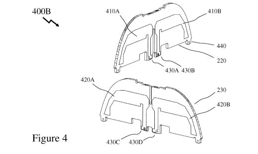
[0031] Figure 4depicts an exploded perspective view of a pair of orthogonally
positioned
dipoles for a GNSS antenna according to an embodiment of the invention;
[0032] Figures 5 and6 depict the pair of dipoles forming the pair of dipoles
for a GNSS antenna
according to an embodiment of the invention;
[0033] Figures 7A depicts a perspective view of a petal assembly comprising an
array of petals
for a GNSS antenna according to an embodiment of the invention;
[0034] Figure 7B depicts a plan perspective schematic view and photograph of
arrays of petals
for GNSS antennae according to embodiments of the invention;
[0035] Figures 7C depicts plan perspective schematic views of an array of
petals for a GNSS
antenna according to an embodiment of the invention;
[0036] Figure 8 depicts a photograph of a GNSS antenna according to an
embodiment of the
invention employing 8 petals within the array of petals;
[0037] Figure 9 depicts a photograph a GNSS antenna according to an embodiment
of the
invention employing 4 petals within the array of petals;
[0038] Figures 10A and 10B depict a plan perspective schematic and photograph
respectively
of an array of petals for a GNSS antenna according to an embodiment of the
invention
employing 4 petals;
[0039] Figure 11 depicts a plan perspective schematic of an array of petals
for a GNSS antenna
according to an embodiment of the invention employing a pair of petals;
[0040] Figure 12 depicts detail for a petal with its tabs for use within a
GNSS antenna
according to an embodiment of the invention;
[0041] Figure 13A depicts a cross-sectional view of an antenna according to an
embodiment
of the invention exploiting a dipole electromagnetically coupled to a pair of
petals;
[0042] Figure 13B depicts dipole structures with dual feed points (FPs) and
single FP with
integrated balun respectively according to embodiments of the invention;
- 13 -
CA 03154668 2022-03-15
WO 2021/046635
PCT/CA2020/051188
[0043] Figures 14 depicts schematics of a dipole and a dipole with ground
plane as
implemented within embodiments of the invention;
[0044] Figure 15 depicts a photograph of a GNSS antenna according to an
embodiment of the
invention and its simulated current distribution;
[0045] Figures 16 and 17 depict the antenna response for right and left hand
circular
polarisations versus elevation for a GNSS antenna according to an embodiment
of the invention
at the GPS L5, GPS L2, Galileo E6 and GPS Li frequencies respectively showing
constant
amplitude response to signals coming at a specific elevation angle regardless
of the azimuth
angle;
[0046] Figure 18 depicts a comparison of a GNSS antenna according to an
embodiment of the
invention with commercial prior art GNSS antennas targeted to the same
application;
[0047] Figure 19 depicts the right hand circular polarisation (RHCP) gain of a
GNSS antenna
according to an embodiment of the invention at zenith and 10 elevation for
all GNSS
frequencies;
[0048] Figure 20 depicts the radiation efficiency of a GNSS antenna according
to an
embodiment of the invention over all GNSS frequencies;
[0049] Figure 21 depicts the axial ratio (AR) for a GNSS antenna according to
an embodiment
of the invention at different elevation angles;
[0050] Figure 22 depicts the AR performance of a GNSS antenna according to an
embodiment
of the invention at horizon compared with commercial prior art GNSS antennas
targeted to the
same application;
[0051] Figure 23 depicts the phase centre variation (PCV) of a GNSS antenna
according to an
embodiment of the invention at horizon compared with commercial prior art GNSS
antennas
targeted to the same application; and
[0052] Figure 24 depicts the results of a CAD for a GNSS antenna according to
an embodiment
of the invention employing a dipole element in conjunction with a pair of
petals.
DETAILED DESCRIPTION
[0053] The present invention is directed to global navigation satellite
systems and more
particularly to antennas, antenna elements and antenna assemblies employing
one or more pairs
of antenna elements each electromagnetically coupled to a dipole with enhanced
azimuthal
performance and/or wide bandwidth high precision high purity reception.
- 14 -
CA 03154668 2022-03-15
WO 2021/046635
PCT/CA2020/051188
[0054] The ensuing description provides representative embodiment(s) only, and
is not
intended to limit the scope, applicability, or configuration of the
disclosure. Rather, the ensuing
description of the embodiment(s) will provide those skilled in the art with an
enabling
description for implementing an embodiment or embodiments of the invention. It
being
understood that various changes can be made in the function and arrangement of
elements
without departing from the spirit and scope as set forth in the appended
claims. Accordingly,
an embodiment is an example or implementation of the inventions and not the
sole
implementation. Various appearances of "one embodiment," "an embodiment" or
"some
embodiments" do not necessarily all refer to the same embodiments. Although
various features
of the invention may be described in the context of a single embodiment, the
features may also
be provided separately or in any suitable combination. Conversely, although
the invention may
be described herein in the context of separate embodiments for clarity, the
invention can also
be implemented in a single embodiment or any combination of embodiments.
[0055] Reference in the specification to "one embodiment", "an embodiment",
"some
embodiments" or "other embodiments" means that a particular feature,
structure, or
characteristic described in connection with the embodiments is included in at
least one
embodiment, but not necessarily all embodiments, of the inventions. The
phraseology and
terminology employed herein is not to be construed as limiting but is for
descriptive purpose
only. It is to be understood that where the claims or specification refer to
"a" or "an" element,
such reference is not to be construed as there being only one of that element.
It is to be
understood that where the specification states that a component feature,
structure, or
characteristic "may", "might", "can" or "could" be included, that particular
component,
feature, structure, or characteristic is not required to be included.
[0056] Reference to terms such as "left", "right", "top", "bottom", "front"
and "back" are
intended for use in respect to the orientation of the particular feature,
structure, or element
within the figures depicting embodiments of the invention. It would be evident
that such
directional terminology with respect to the actual use of a device has no
specific meaning as
the device can be employed in a multiplicity of orientations by the user or
users.
[0057] Reference to terms "including", "comprising", "consisting" and
grammatical variants
thereof do not preclude the addition of one or more components, features,
steps, integers, or
groups thereof and that the terms are not to be construed as specifying
components, features,
steps, or integers. Likewise, the phrase "consisting essentially of', and
grammatical variants
thereof, when used herein is not to be construed as excluding additional
components, steps,
- 15 -
CA 03154668 2022-03-15
WO 2021/046635
PCT/CA2020/051188
features integers or groups thereof but rather that the additional features,
integers, steps,
components or groups thereof do not materially alter the basic and novel
characteristics of the
claimed composition, device or method. If the specification or claims refer to
"an additional"
element, that does not preclude there being more than one of the additional
element.
[0058] Reference to terms such as "perpendicular", "along", "parallel" and
grammatical
variants thereof in respect to alignment and / or direction should be
considered not as absolute
but as having a tolerance to variation thereof such that these directions
and/or alignments are
"substantially" as indicated. Tolerances to these being as established, for
example, through
manufacturing tolerances, performance tolerances, manufacturing costs etc.
[0059] "Azimuth angle" as used herein refers to a rotation angle in the X-Y
plane centered on
the origin, and relative to a defined direction.
[0060] "Elevation angle" or "altitude" as used herein refers to the angle
subtended between the
Poynting vector of the incident plane wave, and the X-Y (ground) plane.
Accordingly, a wave
of grazing incidence from the horizon has a near zero elevation angle whilst a
wave incident
vertically has a 90 degree elevation angle.
[0061] "Axial ratio" as used herein refers to a measure of the extent to which
an antenna is
able to reject circularly polarized signals of the unwanted polarization (a
second rotational
sense) relative to the wanted polarization (a first rotational sense), and is
a measure of the
ability to reject multipath signals which is an important parameter for
precision antennas.
[0062] "Phase center offset" as used herein refers to a concept that there is
a region associated
with an antenna which tends to a point for a perfect antenna, from within
which or at, all signals
may be considered to have been received at or transmitted from. This is a
virtual regioWpoint
in space typically centered just above the midpoint of the physical antenna
and is a measure of
the limits of knowledge of an antenna's position in space.
[0063] "Phase center variation" as used herein refers to a measure of the
apparent phase center
movement over all incident angles for plane waves (i.e. around all azimuths
and all elevation
angles) and over all frequencies in the bandwidth. An ideal antenna having a
phase center
variation of zero.
[0064] A "petal" as used herein refers to a metallized antenna structure
either free-standing,
supported by a frame, patterned onto a substrate, or patented onto a substrate
or carrier
supported by a frame which provides a receiving antenna element for a GNSS
antenna. For
simplicity within the following mechanical description of GNSS antennae
according to
embodiments of the invention the term petal refers to the metallized antenna
structure and any
- 16 -
CA 03154668 2022-03-15
WO 2021/046635
PCT/CA2020/051188
substrate or carrier together with ancillary elements for mechanical
attachment / retention of
the petal discretely or in an array of petals with one or more other elements
of the GNSS
antenna. Within the following functional description of GNSS antennae
according to
embodiments of the invention the term petal refers to the metallized antenna
structure.
[0065] A "dipole antenna" (commonly referred to as a dipole) as used herein
refers to, but is
not limited to, any one of a class of antennas producing a radiation pattern
approximating that
of an elementary electric dipole with a radiating structure supporting a line
current so energized
that the current has only one node at each end.
[0066] A "radome" as used herein refers to, but is not limited to, an
environmental housing or
cover within which an antenna, e.g. a GNSS antenna, is housed which is
transparent to wireless
signals in the frequencies of interest.
[0067] A GNSS "rover" antenna as used herein refers to, but is not limited to,
a GNSS antenna
addressing real-time kinematic (RTK) and mobile (roving) applications.
[0068] A "CubeSat" as used herein refers to, but is not limited to, a U-class
spacecraft which
is a form of miniaturized satellite which is made up of multiples of 10 cm x
10 cm x 10 cm
cubic units (4" x 4" x 4"). A CubeSat may employ commercial off-the-shelf
(COTS)
components for their electronics and structure.
[0069] As discussed above GNSS receivers are employed within a wide range of
applications
within both the civil and military markets. One such dominant configuration
for dual band
receivers for civilian applications is the use of the Li + L2 bands of the GPS
system (formerly
Naystar GPS). The operating frequency bands for GPS Li and GPS L2 being listed
below in
Table 1 together with the frequency bands of the other major GNSS systems
introduced in the
2000s, namely Beidou, Galileo, GLONASS, GPS, and NAVIC.
System B eidou Galileo GLONASS
Owner China Europe Russia
Freq. 1.559-1.563 GHz (B1) 1.164-
1.189 GHz (E5a) 1.593-1.610 GHz (G1)
1.195-1.210 GHz (B2) 1.189-1.214 GHz (E5b) 1.237-
1.254 GHz (G2)
1.256-1.280 GHz (B3) 1.260-1.300 GHz (E6) 1.189-
1.214 GHz (G3)
1.559-1.591 GHz (El)
System GPS NAVIC
Owner USA India
Freq. 1.563-1.587 GHz (L1 signal) 1.164-1.188
GHz (L5 Band)
- 17 -
CA 03154668 2022-03-15
WO 2021/046635
PCT/CA2020/051188
1.215-1.2396 GHz (L2 signal) 2.483-2.500 GHz (S Band)
1.164-1.189 GHz (L5 Band)
Table 1: Operating Frequencies of GNSS Systems (Nearest 1MHz)
[0070] There is also increasing deployment of satellites which also provide a
navigation signal
on the L5 band and accordingly GNSS receivers compatible with the L1 +L5
signals discretely
or L1+ L2 + L5 signals. L5 offers several benefits including, but not limited
to, twice as L2,
being within a band designated by the International Telecommunication Union
(ITU) for the
Aeronautical Radio-Navigation Services (ARNS) which is less prone to
interference with
ground based navigation aids, and sharing the same frequency space as the ESA
signal from
Galileo. Similarly, there is benefit in having GNSS receivers compatible with
the GPS and
Galileo systems, for example, allowing a device comprising such a receiver to
be employed in
regions where one or both GNSS systems are accessible.
[0071] SECTION 1: DESIGN PRINCIPLES
[0072] The design of a GNSS antenna requires consideration of a range of
characteristics
including, for example, the ability for tracking satellites at low elevation,
phase centre variation
(PCV), antenna efficiency and impedance, axial ratio and up-down ratio (UDR),
antenna
bandwidth, etc. whilst also providing a light weight, compact and robust form
factor. Whilst
the following description and embodiments of the invention are directed
towards a GNSS rover
antenna it would be evident to one of skill in the art that the designs and
principles outlined
may be employed in the design and implementation of GNSS antennas for other
applications
and scenarios without departing from the scope of the invention.
[0073] /A: Low Elevation Tracking: The use of Precise Point Positioning (PPP)
and satellite
broadcast of the PPP corrections data has become widely adopted. PPP
correction data is
broadcast from geostationary satellites, which generally subtend low elevation
angles to many
densely populated regions such as Europe and much of North America. The link
margin of L
band signals is typically low (or thin), so that improved gain at these
elevation angles is an
important attribute for a GNSS antenna. This issue is exacerbated at satellite
beam edges and
northern latitudes, where the link margin is further challenged and a
difference of just ldB in
antenna gain or antenna noise figure can make a significant difference in
correction availability.
A key design parameter in this respect is the antenna gain-to-noise
temperature (G/T) which is
the ratio of the antenna element gain divided by the receiver system noise
temperature, typically
determined by the antenna noise figure. For example, the inventors have
targeted a G/T
- 18 -
CA 03154668 2022-03-15
WO 2021/046635
PCT/CA2020/051188
objective for GNSS antenna according to embodiments of the invention of -
25.5dB/K at a 100
elevation angle.
[0074] The gain of most prior art GNSS antenna elements, such as patches and
crossed dipoles,
rolls off rapidly as the elevation angles decreases towards the horizon. The
polarization
response of these prior art GNSS antenna elements also becomes linear at the
lower elevation
angles, due to the existence of a ground plane, necessary to increase gain in
the hemisphere
above the antenna. Improved gain close to the horizon also increases the
ability of the receiver
to track low elevation satellites with a concomitant improvement in the
dilution of precision
parameter (DOP), which is a metric related to pseudorange measurement
accuracy. Most
commercially available GNSS rover antennae for a peak gain at zenith of about
3.5 dBic to 5
dBic with a roll-off at the horizon of 10-12 dB. Typically, this provides an
antenna gain at
horizon, at best, of about ¨5 dBic, which is insufficient for optimized L band
correction usage.
Within the prior art different antenna types such as helical elements have
been proposed to
overcome this issue, but their cylindrical shape and longer length makes them
unsuitable for
many applications, particularly roving (or rover) applications. Furthermore,
the helix suffers
from back lobes that can make the antenna more susceptible to reception of
multipath signals
incident below the positive hemisphere of the antenna.
[0075] Accordingly, as evident in Sections 2 and 3 the inventors have
established a GNSS
rover antenna exploiting wide bandwidth radiating elements (hereinafter
referred to as "petals")
which surround a distributed feed network in order to achieve superior Right
Hand Circular
Polarized (RHCP) gain at low elevation angles in a high performance GNSS
antenna with small
form factor yet with an assembly providing increased ease of manufacture and
improved
reproducibility.
[0076] IB: Phase Centre Variation (PCV): The phase centre of an ideal antenna
is a notional
point in space at which all signals are received or transmitted from,
independent of the
frequency, or elevation or azimuth angle of signal incidence. However, the
phase centres of
real life antennas are less tidy, and the PCV is a measure of the variation of
the "zero" phase
point as a function of frequency, elevation, and azimuth angles. Correction
data for phase center
variation is commonly encoded in a standardized file, e.g. an Antenna Exchange
Format
(ANTEX) file, which can be applied concurrently for precision applications.
The azimuthal
orientation of rover antennas is typically unknown so that errors for specific
azimuth angles
cannot be accounted for. The PCV corrections data provided in the ANTEX file
are usually
provided as a function of elevation and frequency, but with averaged azimuth
data for each
- 19 -
CA 03154668 2022-03-15
WO 2021/046635
PCT/CA2020/051188
elevation and frequency (designated "noazi" corrections). Thus, corrections
can be applied for
each frequency and elevation angle but errors due to the variation in the
azimuthal PCV cannot
be corrected in the receiver. For RTK systems, the net system error is the RMS
sum of the base
and rover antenna phase center variations. It is usually possible to
accommodate larger base
station antennas, which can commonly provide PCVs approaching +/- 1 mm (e.g.
from
Tallysman VeraPhaseTM or VeraChokeTM antennas). However, in many instances
the
accuracy of the combined system is largely determined by the PCV of the
smaller GNSS rover
antenna. Thus, even with corrections data, azimuthal symmetry in the GNSS
antenna is key.
Accordingly, the design approach employed by the inventors focused on symmetry
for both
the antenna element structure and mechanical housing design.
[0077] IC: Antenna Efficiency and Impedance: Antenna Efficiency (AE) can be
narrowly
defined in terms of copper losses of the radiating elements but feed network
losses also
contribute and accordingly, a design objective should be the optimization of
both. It is generally
known by those of skill in the art that physically wide radiating elements are
a key requirement
for wider bandwidth and that copper presents a good compromise for the
radiator metal. Within
the design as described below in Section 2 wide physical petals are employed
although it would
be evident that in narrow band applications alternate petal designs with
narrower geometries
may be employed without departing from the scope of the invention. Similarly,
the
experimental results described in Section 3 exploit copper as the petal
metallization although
it would be evident that other materials may be employed including, for
example, silver offers
improved conductivity but is expensive.
[0078] However, as will be evident from Section 2 the GNSS antenna according
to
embodiments of the invention the petals are parasitic resonators that are
tightly coupled to a
distributed feed network, which in itself is intrinsically narrowband.
Accordingly, the resulting
wide bandwidth response of the GNSS antenna according to embodiments of the
invention
results from the load on the feed network provided by the excellent wideband
radiation
resistance of the petals.
[0079] This arrangement was chosen because the resulting impedance at the de-
embedded
antenna feed terminals is close to the ideal impedance required (50 Ohms),
thus requiring
minimal impedance matching. The near ideal match over a wide bandwidth is
important
because it allows the impedance to be transformed to ideal using a very short
transmission line,
typically less than lambda/4, that can include an embedded infinite balun.
- 20 -
CA 03154668 2022-03-15
WO 2021/046635
PCT/CA2020/051188
[0080] Within the embodiments of the invention described and depicted in
respect of Figures
lA to 10B below in Section 2 petals are employed in conjunction with a dipole
for each
orthogonal exciter axis wherein the pair of orthogonal exciter axes are
electrically independent
and highly isolated electrically (better than -30dB within fabricated GNSS
antenna according
to embodiments of the invention), even with the parasitic petal coupling. To
achieve a desired
circular polarization, the two axis are then driven independently, in phase
quadrature as derived
from hybrid couplers, for example, within the associated microwave/RF circuit
associated with
the GNSS antenna which may be implemented upon a PCB forming part of the GNSS
antenna
or an external circuit. As will be evident from the results presented in
Section 4 the resulting
GNSS antenna according to embodiments of the invention combining inherently
efficient
parasitic petals combined with a low loss distributed feed network result in a
highly efficient
GNSS antenna structure offering superior performance to prior art solutions.
[0081] 1D: Axial Ratio (AR) and Up-Down Ratio (UDR): AR characterizes the
performance
of the antenna's ability to receive circular signals whilst the UDR is the
ratio of gain pattern
amplitude at a positive elevation angle (a) to the maximum gain pattern
amplitude at its mirror
image (-a). Good AR and UDR across the full bandwidth of the antenna is
required to ensure
the purity of the reception of the RHCP signals within GNSS systems and to
mitigate multipath
effects. GNSS signals reflected from the ground, buildings, or metallic
structures such as
vehicles are delayed and the purity of their RHCP signals is degraded with
Left Hand Circular
Polarized (LHCP) signals. As GNSS antenna according to embodiments of the
invention were
designed to provide improved gain at low elevation angles, a very low AR and a
high UDR are
particularly important to mitigate multipath interference.
[0082] 1E: Wide Antenna Bandwidth: A wide GNSS bandwidth antenna allows the
system
employing it to achieve positioning based on GNSS signals from multiple
constellations, e.g.
satellites from multiple GNSS systems. Recent research has shown that
interoperability
between different satellite constellations can significantly improve
navigation and positioning
performance. In particular, it has been shown that a wide bandwidth GNSS
antenna allows for
the implementation of three-carrier and multicarrier ambiguity resolution
techniques to obtain
the highest possible precision. In challenging environments where some signals
may be
blocked from time to time by foliage, buildings, etc. then these blocked
signals may be replaced
by signals from satellites in other constellations that are not subject to
such blockage.
Accordingly, it would be beneficial for a GNSS antenna to be capable of
reception over the
full GNSS frequency bandwidth from 1.15GHz to 1.60GHz.
- 21 -
CA 03154668 2022-03-15
WO 2021/046635
PCT/CA2020/051188
[0083] IF: Lightweight, Robust and Compact: There is continuous pressure for
smaller GNSS
antennas, but precision rover GNSS antennas are typically required to receive
signals in both
the low and high GNSS frequency bands. There is an unescapable constraint that
limits the
bandwidth of small antennas, so that in order to provide a full bandwidth
rover GNSS antennas,
unavoidably, tend to be larger. Accordingly, being ever mindful of performance
additional
mechanical objectives were established by the inventors for embodiments of the
invention
although it would be evident that such mechanical constraints may be different
within other
systems and hence GNSS antenna with different configurations may be employed
but still
exploiting the design concepts and methodologies outlined within this
specification and remain
within the scope of the invention.
[0084] According, the GNSS antenna according to an embodiment of the invention
whose
results are presented in Section 4 were for a small and light weight radiating
element (given
the full bandwidth requirement) with a ground plane size of approximately 100
mm (4 inches),
an element height of 30mm or lower (1.2" or lower), and a weight of 100 grams
or less (3.5
ounces or less). It would be evident that smaller versions of this GNSS
antenna may be
implemented exploiting embodiments of the invention albeit with different
performance.
Applications for GNSS antennas according to embodiments of the invention may
include, but
not be limited to, housed antennas (such as RTK rovers) and also a lightweight
antennae
suitable for mobile applications like such as drones, UAVs, CubeSats, etc.
[0085] Within the following description with respect to embodiments of the
invention as
described and depicted with respect to Figures 1 to 24 then the inventors have
established an
antenna design methodology to achieve the performance objections outlined in
Section 1, these
being antenna elements and systems which employ dipole feed(s). The following
description
is split into Section 2 to 5 respectively wherein:
= Section 2 relates to the mechanical design of dipole fed antenna elements
and
systems according to embodiments of the invention;
= Section 3 relates to the operating principles of dipole fed antenna
elements and
systems according to embodiments of the invention;
= Section 4 relates to the performance of dipole fed antenna elements and
systems
according to embodiments of the invention; and
= Section 5 relates to comparison of dipole fed antenna elements and
systems
according to embodiments of the invention to the prior art.
- 22 -
CA 03154668 2022-03-15
WO 2021/046635
PCT/CA2020/051188
[0086] SECTION 2: MECHNICAL DESIGN OF DIPOLE FED ANTENNA
ELEMENTS AND SYSTEMS
[0087] Within the following description with respect to Figures 1 to 15
embodiments of the
invention with respect to GNSS antenna structures are described. As discussed
above in Section
1 there are several performance aspects of GNSS antennas where it is desirable
to concurrently
optimize performance. The underlying design principles of GNSS antennas
according to
embodiments of the invention are described below in Section 4 with respect to
Figures 14-15
whilst the performance of prototype GNSS antennas exemplary embodiments of the
invention
are presented below in Section 3 with respect to Figures 16-22. The design
principle established
by the inventors therefore comprises of radiating petals which are
electromagnetically (i.e.
raliatively) coupled to a dipole.
[0088] Accordingly, referring to Figure 13A the minimum structure for an
antenna is depicted
in cross-sectional view 1300A embodying these design elements is presented
comprising a pair
of Petals 110 with a dipole formed from first and second Dipole Elements 1320A
and 1330A.
As depicted the first and second Dipole Elements 1320A and 1320B are formed
upon a Carrier
1310A, e.g. a PCB, and are coupled to first and second feed points (FPs) 1330A
and 1330B
respectively. A plan view 1100 of the pair of petals 110 is depicted in Figure
11 with the two
Petals 110 evident opposite each other with a common central axis X-X which
would be aligned
with the carrier 1310 and the first and second dipole elements 1310A and 1310B
respectively.
Also depicted in plan view 1100 at the distal ends of each Petal 110 are a
pair of Tabs 130 as
described below in respect of Figure 1 and Solder Pads 1010 as described below
in respect of
Figure 10. As depicted the pair of Petals 110 are joined via an unmetallized
portion of the
carrier, Element 1110, which the Petals 110 have been formed upon.
[0089] Referring to Figure 13B there are depicted first and second electrical
configurations
1300B and 1300C respectively for coupling a dipole to an external electrical
circuit. In first
electrical configuration 1300B a first Dipole Element 1340A is coupled to a
first FP 1360A via
first Track 1350A which is part of a first Transmission Line 1355A between the
first FP 1360A
and the first Dipole Element 1340A. Similarly, a second Dipole Element 1340B
is coupled to
a second FP 1360B via second Track 1350B which is part of a second
Transmission Line 1355B
between the second FP 1360B and the second Dipole Element 1340B. Accordingly,
the dipole
depicted in first electrical configuration 1300A is driven through both first
FP 1360A and
second FP 1360B. Optionally, the first and second Dipole Elements 1320A and
1320B are also
implemented on the other side of the Carrier 1310B where the two electrical
structures on either
-23 -
CA 03154668 2022-03-15
WO 2021/046635
PCT/CA2020/051188
side of the Carrier 1310B are electrically connected through a plurality of
vias, not depicted for
clarity.
[0090] In second electrical configuration 1300C a first Dipole Element 1370A
is coupled to a
first FP 1390A via first Feed Track385A and a second Dipole Element 1370B is
coupled to a
second Feed Track385B. Also depicted coupled to the first FP 1390A and the
second Dipole
Element 1370B is a first Transmission Line 1380A which terminates in Pad 1395
upon the
second Dipole Element 1370B. Accordingly, in contrast to first electrical
connection 1300B
where dipole comprising the first and second Dipole Elements 1340A and 1340B
are each
coupled to unbalanced lines from the first and second FPs 1360A to 1360B the
dipole in second
electrical configuration 1300C is fed from a single FP 1390 and incorporates a
balanced-
unbalanced (balun) connection so that the first and second Dipole Elements
1370A and 1370B
operate in a balanced manner with an unbalanced feed from first FP 1390A.
[0091] Beneficially, in contrast to first electrical configuration 1300B the
integrated balun in
second electrical configuration 1300C has an electrical impedance close to a
target 50 S2
impedance where matching to the target 50 S2 impedance at the FP 1390A is
achieved through
the appropriate design parameters for the transmission line comprising first
Feed Track385A
and first Transmission Line 1380A. Optionally, the first and second Dipole
Elements 1370A
and 1370B with or without the first and second Feed Tracks385A and 1385B
respectively are
also implemented on the other side of the Carrier 1310B where the two
electrical structures on
either side of the Carrier 1310C are electrically connected through a
plurality of vias, not
depicted for clarity.
[0092] These GNSS antenna employing receiving elements each comprising a pair
of opposing
petals which are electromagnetically coupled to a dipole and therein to an RF
receiver circuit.
Subsequently, an overview of the operating principle of a GNSS antenna
employing said
receiving elements comprising a pair of opposing petals which are
electromagnetically coupled
to a dipole is presented.
[0093] Referring to Figures 1A and 1B there are depicted lower and upper
perspective views
100A and 100B respectively of a GNSS antenna according to an embodiment of the
invention.
Considering initially lower perspective view 100A of a GNSS Antenna according
to an
embodiment of the invention in Figure lA an array of Petals 110 is mounted to
a printed circuit
board (PCB) 120 via Tabs 130 on the Petals 110 inserted into slots within the
PCB 120. This
mounting of a substrate upon which the Petals 110 form metallized regions
being depicted and
described below in more detail with respect to Figure 12. Disposed upon the
PCB 120 is
- 24 -
CA 03154668 2022-03-15
WO 2021/046635
PCT/CA2020/051188
Electronics 140 which is coupled to RF Connector 150 and to a plurality of
dipoles, not visible
within lower perspective view 100A but disposed within the GNSS antenna
according to an
embodiment of the invention. Now referring to upper perspective view 100B of
the GNSS
Antenna according to an embodiment of the invention in Figure 1B the array of
Petals 110 is
similarly depicted mounted to a printed circuit board (PCB) 120. As depicted
in Figure 1B the
array of Petals 110 comprises eight (8) Petals 110 although as described and
depicted below in
respect of Figures 10 to 12 an antenna exploiting embodiments of the invention
may employ 2
or 4 Petals 110. However, other counts of Petals 110 may be employed where N,
the number
of Petals 110, is an even integer. Also depicted in Figure 1B are Mounting
Holes 160 within
the PCB 120 for attaching the antenna to a radome, base of a radome, a choke
ring etc.
[0094] Within Figures 1A and 1B are first and second Artefacts 170A and 170B
which are
artefacts arising from the computer aided design (CAD) software employed in
generating the
images presented within Figures 1A to 6 respectively, Figures 6A to 7B
respectively, and
Figure 8. First Artefacts 170A being the sides of elements within the array of
Petals 110 which
support the carrier(s) and/or substrate(s) onto which the array of Petals 110
is implemented via
metallization and/or the Petals 110 directly. Second Artefacts 170B being the
tops of these
elements. As such first and second Artefacts 170A and 170B arise due to the
CAD software
treating the carrier for the array of Petals 110 and/or the Petals 110 as
transparent.
[0095] The Electronics 140 provides a microwave / RF circuit which, in the
instance that the
GNSS antenna is a receiver, combines the received RF / microwave signals at
the feed points
(FPs) of the plurality of dipoles to generate an RF/microwave output signal
coupled to the RF
Connector 150. Accordingly, considering the instance of a pair of dipoles
disposed at right
angles to one another then there are 4 FPs. The Electronics 140 thereby
comprises a pair of
hybrid couplers, which each couple the RF/microwave signals from a pair of FPs
to a common
output port, and a balun, which receives the signals from the common output
ports of the pair
of hybrid couplers and combines them to generate the signal coupled to the RF
Connector 150
at the output of the Balun. Where the microwave / RF signals from the FPs have
a relative
phase difference sequentially of 0 , 90 , 180 , and 270 then these signals
are initially
combined within each of the hybrid couplers and then within the Balun.
Accordingly, based
upon this described sequence of phases coupled from the FPs to the hybrid
couplers the GNSS
antenna may operate to receive right hand circularly polarized signals.
Alternatively, the GNSS
antenna may be configured to receive left hand circularly polarized signals or
within other
embodiments of the invention provide a GNSS antenna for a transmitter
generating right hand
- 25 -
CA 03154668 2022-03-15
WO 2021/046635
PCT/CA2020/051188
polarized signals or left hand polarized signals. Optionally, within other
embodiments of the
invention the Balun may be a transformer. Within Figure 1 A the four FPs are
located within
Region 180 projecting through the PCB 120.
[0096] Whilst the embodiments of the invention described and depicted below in
respect of
Figures 2 to 10B employ a pair of orthogonally disposed dipoles providing 4
FPs with each
dipole coupled to a pair of Petals 110 such that the GNSS antenna operates
with relative phase
differences of 0 , 90 , 180 , and 270 other configurations may be implemented
without
departing from the scope of the invention. For example, as described above and
depicted in
Figure 13B with respect to second electrical configuration 1300C, the dipoles
may employ
integrated baluns such that only a pair of FPs are required, one for each
dipole, where the balun
provides the out-of-phase phase differences for the pair of dipole elements
within each dipole.
Further, as described and depicted in Figures 11 and 13A an antenna may employ
a single
dipole with a single pair of Petals 110. Within another configuration an
antenna may employ
three dipoles mounted at 120 to each other with 6 Petals 110 such that the
antenna receives or
transmits signals with relative phase differences of 0 , 60 , 120 , 180 , 240
and 270 . It would
be evident that other configurations could be implemented without departing
from the scope of
the invention.
[0097] Now referring to Figures 2 there is depicted a lower perspective view
200A of a GNSS
antenna according to an embodiment of the invention with the PCB 120removed.
Accordingly,
Figure 2 depicts a similar perspective to that of lower perspective view 100A
in Figure lA with
the PCB 120 removed. Accordingly, the array of Petals 110 is depicted together
with the first
Artefacts 170A. Also depicted is an Isolation Block 240 through the bottom of
which project
the FPs within Region 180. The FPs being formed upon the dipoles, a pair of
FPs being
disposed upon a first circuit board Dipole A 220 and a further pair of FPs
disposed upon a
second circuit board Dipole B 230. Dipole A 220 and Dipole B 230 being
disposed
orthogonally to one another. Also depicted are first to fourth Supports 210A
to 210D where
these are disposed radially within the GNSS antenna. Each of the first to
fourth Supports 210A
to 210D being disposed between one end of Dipole A 220 and an end of Dipole B
230.
Accordingly, the first to fourth Supports 210A to 210D support additional
Petals 110 within
the array of Petals 110 which are disposed between the Petals 110 associated
with the Dipole
A 220 and Dipole B 230.
[0098] Referring to Figure 3 there is depicted an upper perspective view 300
of a GNSS
antenna according to an embodiment of the invention with the array of Petals
110 removed.
- 26 -
CA 03154668 2022-03-15
WO 2021/046635
PCT/CA2020/051188
Accordingly, Figure 3 depicts a similar perspective to that of upper
perspective view 100B in
Figure 1B with the array of Petals 110 removed. Accordingly, there are
depicted the
orthogonally disposed Dipole A 220 and Dipole B 230 together with the first to
fourth Supports
210A to 210D respectively. Located at the centre is Isolation Block 240. It
would be evident
from lower perspective view 100A in Figure 1A, lower perspective view 200 in
Figure 2
respectively, and upper perspective view 300A in Figure 3 that an outer end of
each of the
Dipole A 220, Dipole B 230, and first to fourth Supports 210A and 210D
comprises a projection
which fits within a slot within the PCB 120 locating each outer end.
[0099] The middle portion of each of Dipole A 220 and Dipole B 230 comprises
FPs which
similarly fit through slots within the PCB 120 in the Region 150 and engage
with slots formed
within the Isolation Block 240. The lower inner ends of each of the first to
fourth Supports
210A to 210D also engage with features on the external surface of the
Isolation Block 240.
The orientation of each of the Dipole A 220, Dipole B 230 and first to fourth
Supports 210A
to 210D respectively being defined by these engagements with the PCB 120 and
Isolation
Block 240 and the Support Frame 310 where the upper region of each of these
elements engages
a slot within the Support Frame 310. Accordingly, each of the Dipole A 220,
Dipole B 230 and
first to fourth Supports 210A to 210D respectively are orientated
substantially perpendicular
to the PCB 120. It would be evident to one of skill in the art that other
mechanical means to
locate, orientate and retain the Dipole A 220, Dipole B 230 and the first to
fourth Supports
210A and 210D may be employed without departing from the scope of the
invention.
[00100] Now
referring to Figure 3B there is depicted a partially exploded assembly
300B of the Dipole A 220, Dipole B 230, first to fourth Supports 210A to 210D
and Mounting
Block 240 for a GNSS antenna according to an embodiment of the invention.
Evident on the
Mounting Block 240 are the slots allowing insertion of the Dipole A 220 and
Dipole B 230 so
that the FPs project through the bottom of the Mounting Block 240 and therein
the PCB 120 in
the final assembly. Also evident are the slots for engaging the inner lower
portions of the first
to fourth Supports 210A to 210D respectively.
[00101] In addition to providing a mechanical alignment of Dipole A 220 and
Dipole B 230
the Mounting Block 240 also provides a benefit in the microwave/RF domain for
performance
of a GNSS antenna according to an embodiment of the invention. As evident in
Figures 3B-6
respectively each of Dipole A 220 and Dipole B 230 is depicted as being
configured according
to the description above and as depicted in respect of second electrical
configuration 1300C in
Figure 13 with the exception that the transmission line, balun etc. have been
omitted for clarity.
- 27 -
CA 03154668 2022-03-15
WO 2021/046635
PCT/CA2020/051188
Accordingly, when assembled Dipole A 220 and Dipole B 230 have disposed closed
to the
point they intersect a pair of metallized lines (one from each of Dipole A 220
and Dipole B
230) run vertically parallel to one another thereby forming another parasitic
transmission line
through the intervening medium, e.g. air where no Mounting Block 240 is
provided. Where the
metallization is only on one side of each of Dipole A 220 and Dipole B 230
then a single
parasitic transmission line may be formed whilst when both sides of each of
Dipole A 220 and
Dipole B 230 are metallized then four parasitic transmission lines may be
formed. Where the
dielectric between these parallel traces on Dipole A 220 and Dipole B 230 is
air then the
frequency at which these parasitic transmission lines "operate" may be within
the operating
frequency range of the GNSS antenna resulting in unwanted coupling, crosstalk,
and loss etc.
Accordingly, the Mounting Block 240 provides a different dielectric constant
for part or all of
each parasitic transmission line wherein appropriate selection of the material
and hence
dielectric constant of the Mounting Block 240 the es the frequency at which
these parasitic
transmissions lines "operate" outside the operating frequency range of the
GNSS antenna.
[00102] Now referring to Figures 4 there is depicted an exploded perspective
view 400 of a
pair of orthogonally positioned dipoles for a GNSS antenna according to an
embodiment of the
invention.
[00103] Within exploded perspective view 400 Dipole A 220 and Dipole B 230 are
depicted
separated vertically. Dipole A 220 having first and second Dipole
Metallizations 410A and
410B each forming one half of a dipole. First Dipole Metallization 410A being
electrically
coupled to first FP 430A at the left central lower portion of Dipole A 220
whilst second Dipole
Metallization 410B is electrically coupled to second FP 430B at the right
central lower portion
of Dipole A 220. Similarly, third Dipole Metallization 420A is electrically
coupled to third FP
430C at the left central lower portion of Dipole B 230 whilst fourth Dipole
Metallization 420B
is electrically coupled to fourth FP 430D at the right central lower portion
of Dipole B 230.
First to fourth FPs 430A to 430D being the FPs evident within the central
Region 180 in lower
perspective view 100A in Figure 1 and lower perspective views 200A and 200B in
Figures 2
and 2B respectively. Also depicted in assembled and exploded perspective views
400A and
400B in Figures 4 and 4B respectively are Mounting Tabs 440 at the outer lower
portion of
each of Dipole A 220 and Dipole B 230. The Mounting Tabs 440 engaging slots
within the
PCB 120 for mounting the Dipole A 220 and Dipole B 230 to the PCB 120 and
defining their
relative orientation through the precision of the slots within the PCB 120
being at 90 to one
another for mounting Dipole A 220 and Dipole B 230 respectively.
- 28 -
CA 03154668 2022-03-15
WO 2021/046635
PCT/CA2020/051188
[00104] Alternatively, within another embodiment of the invention such as
described above
and depicted in Figure 13B with respect to second electrical configuration
1300C, the dipoles
may employ integrated baluns such that only a pair of FPs are required, one
for each dipole.
Accordingly, in this configuration the second FP 230B and third FP 230C may be
coupled to
the external microwave/RF circuit such that the first and second Dipole
Metallizations 410A
and 410B are coupled via the integrated balun (not shown for clarity) to
second FP 430B and
third and fourth Dipole Metallizations 420A and 420B are coupled via another
integrated balun
(not shown for clarity) to third FP 430C. Within other embodiments of the
invention second
FP 430B may be replaced with first FP 430A and/or third FP 430C may be
replaced with fourth
FP 430D where the integrated baluns are employed.
[00105] As depicted Dipole A 220 and Dipole B 230 have interlocking slots that
provide for
assembly of the crossed dipole arrangement according to an embodiment of the
invention.
However, within other embodiments of the invention other assembly
configurations may be
employed without departing from the scope of the invention to provide the pair
of crossed
dipoles using 2, 3, or 4 elements and other means of attachment and assembly
without departing
from the scope of the invention. The upper central edges of Dipole A 220 and
Dipole B 230 as
depicted within the embodiment of the invention are profiled to include an
indent to support a
stiffener attached to the flexible circuit forming the array of Petals 110
such as Support Frame
310 depicted and described above in respect of Figure 3. The upper edges of
Dipole A 220 and
Dipole B 230 provide mechanical support for the respective Petals 110 of the
array of Petals
110 to which they are associated. The array of Petals 110 , may, within an
embodiment of the
invention be formed from a semi-flexible or flexible PCB with the array of
Petals 110 imprinted
in metallization upon the semi-flexible or flexible PCB.
[00106] By appropriate design and attachment of the array of Petals 110 within
the GNSS
antenna relative to the Dipole A 220 and Dipole B 230 then the semi-flexible
or flexible PCB
and hence the array of Petals 110 are in mechanical contact with the upper
edges of Dipole A
220 and Dipole B 230 such that the electromagnetic coupling between the narrow
band dipoles,
Dipole A 220 and Dipole B 230, and the opposed metallized Petals 110 is
determined by the
predetermined distance between the metallized Petals 110 and the metallized
dipoles imprinted
on the dipoles thereby implementing a distributed feed network, wherein each
of the metallized
petals are devoid of direct connection to the external microwave/RF circuit,
such as Electronics
140 depicted in Figure 1A.
- 29 -
CA 03154668 2022-03-15
WO 2021/046635
PCT/CA2020/051188
[00107] Accordingly, referring to Figures 5 and 6 there are depicted first and
second images
500 and 600 respectively for the pair of dipoles for a GNSS antenna according
to an
embodiment of the invention. Referring to first image 500 in Figure 5 there is
depicted a
schematic of Dipole A 220 showing first Dipole Metallization 410A electrically
coupled to
first FP 430A at the left central lower portion of Dipole A 220 whilst second
Dipole
Metallization 410B is electrically coupled to second FP 430B at the right
central lower portion
of Dipole A 220. Also depicted is first Slot 510 which allows Dipole A 220 to
be assembled
with the Dipole B 230 which has a corresponding second Slot 520. Further, as
described in
respect of first and second electrical configurations 1300B and 1300C
respectively in Figure
13B the Dipole A 220 may also have first and second Dipole Metallizations 410A
and 410B
implemented on the other side of Dipole A 220 where these two sides are
electrically connected
through a plurality of vias.
[00108] Referring to second image 600 in Figure 6 there is depicted a
schematic of Dipole B
230 showing third Dipole Metallization 420A electrically coupled to third FP
430C at the left
central lower portion of Dipole B 230 whilst fourth Dipole Metallization 420B
is electrically
coupled to fourth FP 430D at the right central lower portion of Dipole B 230.
Also depicted is
second Slot 520 which allows Dipole B 230 to be assembled with the Dipole A
220 which has
a corresponding first Slot 510. Further, as described in respect of first and
second electrical
configurations 1300B and 1300C respectively in Figure 13B the Dipole B 230 may
also have
third and fourth Dipole Metallizations 420A and 420B implemented on the other
side of Dipole
A 220 where these two sides are electrically connected through a plurality of
vias.
[00109] The first image 500 in Figure 5 and second image 600 in Figure 6
representing Dipole
A 220 and Dipole B 230 for the configuration described and depicted in respect
of second
electrical configuration 1300C in Figure 13B wherein each of Dipole A 220 and
Dipole B 230
comprise integrated baluns. In each of first image 500 in Figure 5 and second
image 600 in
Figure 6 only the ground tracks are depicted and the microstrip feed line,
first Transmission
Line 1380A and its electrical connection to the dipole element, Pad 1395, are
omitted for
clarity. Accordingly, referring to first image 500 in Figure 5 the first
Dipole Metallization 410A
is coupled to first FP 430A via a first Trace 530A and the second Dipole
Metallization 410B is
coupled to second FP 430A via a second Trace 530B. Similarly, third Dipole
Metallization
420A is coupled to third FP 430C via a third Trace 540A and the fourth Dipole
Metallization
420B is coupled to fourth FP 430D via a second Trace 540B. The microstrip
line, not depicted
for clarity, for Dipole A 220 is coupled to the external microwave/RF feed at
first Coupling
- 30 -
CA 03154668 2022-03-15
WO 2021/046635
PCT/CA2020/051188
Point 550. Similarly, the microstrip line, not depicted for clarity, for
Dipole B 230 is coupled
to the external microwave/RF feed at second Coupling Point 560. In this
configuration the first
FP 430A and fourth FP 430D are connected to ground and each of Dipole A 220
and Dipole B
230 are each connected to a single microwave/RF signal. In this configuration
an external
microwave/RF feed network provides or receives 2 microwave/RF signals to an
antenna
comprising Dipole A 220 and Dipole B 230.
[00110] Within an alternate embodiment of the invention Dipole A 220 and
Dipole B 230 do
not include integrated baluns. Accordingly, the first Trace 530A and second
Trace 530B may
be symmetrical mirror images and each is connected to its respective first and
second FPs 430A
and 430B respectively such that a pair of microwave/RF signals are coupled
to/from Dipole A
220. Similarly, the third Trace 530A and fourth Trace 530B may be symmetrical
mirror images
and each is connected to its respective third and fourth FPs 430C and 430D
respectively such
that a pair of microwave/RF signals are coupled to/from Dipole B 230. In this
configuration an
external microwave/RF feed network provides or receives 4 microwave/RF signals
to an
antenna comprising Dipole A 220 and Dipole B 230.
[00111] As depicted in first image 500 in Figure 5 the lower edge of Dipole A
220 comprises
first FP 430A and second FP 430B towards the center and Mounting Tabs 440 at
the outer
edges. The upper edge defines a central region for supporting a stiffener,
e.g. Support Frame
310, and the array of Petals 110 whilst the outer upper edges define the
curved surfaces to
which the array of Petals 110 conforms when attached. Similarly, as depicted
in second image
600 in Figure 6 the lower edge of Dipole B 230 comprises third FP 430C and
fourth FP 430D
towards the center and Mounting Tabs 440 at the outer edges. The upper edge
defines a central
region for supporting a stiffener, e.g. Support Frame 310, and the array of
Petals 110 whilst the
outer upper edges define the curved surfaces to which the array of Petals 110
conforms when
attached.
[00112] As noted above a first dipole of the pair of cross dipoles, Dipole A
220, is formed
from the first and second Dipole Metallizations 410A and 410B respectively
whilst the second
dipole, Dipole B 230, is formed from third and fourth Dipole Metallizations
420A and 420B
respectively. Considering an embodiment of the invention where Dipole A 220
and Dipole B
230 are formed upon a Dipole PCB then each dipole thereby comprises a pair of
centrally
disposed vertical metal traces which connect to the dipole elements at the
inner end of each
dipole metallization trace. The dipole PCB may be of substantially equal
thicknesses to
attachment slots within the PCB 120 to allow for accurate mounting of the
dipoles relative to
-31 -
CA 03154668 2022-03-15
WO 2021/046635
PCT/CA2020/051188
the ground plane formed within or upon PCB 120. Optionally, each Dipole PCB
may include
identical copies of a balun.
[00113] As noted above the upper edges of Dipole A 220 and Dipole B 230 define
the
predetermined distance between the metallized Petals 110 and the metallized
dipoles imprinted
on the dipoles thereby implementing a distributed feed network between the
dipoles and Petals
110. In this manner the Petals 110 are devoid of a direct connection to the
FPs and the
microwave/RF circuit. However, it would be evident from Figures 5 and 6 that
within the
embodiment of the invention presented the dipoles vary in geometry radially
and that the
separation of the dipole metallization from the Petal 110 associated with it
varies radially or
from a different perspective varies with elevation angle. This separation of
petal-dipole
separation as a function of elevation angle being predetermined in dependence
upon the GNSS
antenna design such that either the upper edge of dipole elements is defined
from the petal
geometry or vice-versa. It would also be evident that the length of the dipole
elements from
their inner edge towards the middle of each of Dipole A 220 and Dipole B 230
to their outer
point at the lower outer region of each of Dipole A 220 and Dipole 230 is
determined by the
requirement for the dipole elements to be electrically XJ4 at the central
frequency of the GNSS
antenna. The inventors also established that whilst meeting this requirement
and implementing
the associated Petals 110 that the sensitivity of the impedance of the
structure was less sensitive
to the distance between the Petal 110 and dipole element towards the centre of
the dipole
allowing for increased flexibility in the overall design for the geometry of
the Petals 110
relative to dipole. Accordingly, as visible in Figures 5 the distance of the
upper edge of the
dipole elements relative to the upper edge of the PCB they are formed upon
varies. However,
within other embodiments of the invention this separation between dipole
metallization and
Petal 110 may be constant.
[00114] Now referring to Figures 7A there is depicted a perspective view 700A
of the array
of Petals 110, namely a petal assembly, for a GNSS antenna according to an
embodiment of
the invention. As depicted the array of Petals 110 comprises 8 Petals 110
which are metallized
regions upon an insulating Former 710. At the lower end of each Petal 110 are
a pair of Tabs
130 which as described and depicted in Figure 1A are employed to mount and
attach the Petals
110 to the PCB 120, not depicted for clarity. Within the embodiment of the
invention depicted
metallization upon the Tabs 130 may be soldered to the PCB 120. This
metallization upon the
Tabs 130 being electrically isolated from the metallization forming the Petals
110. Within an
embodiment of the invention the metallization on the Tabs 130 is connected to
a ground plane
-32 -
CA 03154668 2022-03-15
WO 2021/046635
PCT/CA2020/051188
of the PCB 120. It would be evident that within other embodiments of the
invention the lower
ends of the Petals 110 may be attached to the PCB 120 by other means including
mechanical
retention, mechanical attachment, or attachment via a material such as a
resin, glue, or epoxy.
Within other embodiments of the invention the Petals 110 may be mechanically
retained in
position by one or more additional elements mounted external to the Petals 110
connected to
the PCB 120 and/or Dipole A 220 / Dipole B 230 and/or the first to fourth
Supports 210A to
210D respectively without the use of projections such as Tabs 130.
[00115] Referring to Figure 7B there are depicted a plan perspective schematic
view 700B
and a photograph 700C of arrays of petals for GNSS antennae according to
embodiments of
the invention. Referring to schematic view 700B there an array of Petals 710
is depicted
comprising 8 Petals 710. In this instance, the ends of the Petals 710 from the
center end in Tabs
720. Photograph 700C depicts a photograph of an array of Petals 730 according
to an
embodiment of the invention which do not have end tabs as the Petals 730 are
retained by a
mechanical means, e.g. a circular projection above the PCB 120 against which
the Petals 730
push when flexed and mounted at the center.
[00116] Now referring to Figure 7C there are depicted plan schematics in
assembled and
unassembled views 700D and 700E respectively for an array of Petals 740 for a
GNSS antenna
according to an embodiment of the invention. As depicted in assembled view
700D each Petal
740 has a Tab 750 at a distal end from the centre of the array of Petals 740
and a Support Frame
760. In unassembled view 700E in Figure 7C the then Array 700 comprises the
array of Petals
740 for a GNSS antenna according to an embodiment of the invention and is
depicted separate
from the Support Frame 760. Within other embodiments of the invention the
Support Frame
760 may be omitted. Support Frame 760 may provide Support Frame 310 as
depicted in Figure
3 which engages the upper central portions of the dipole PCBs and/or supports.
Optionally,
within other embodiments of the invention the Support Frame 760 may be
integrated as part of
the array of petals.
[00117] When the Central Support 760 is used, such as depicted in Figure 3
with Support
Frame 310, the shape of the upper edge of Dipole A 220, Dipole B 230, and
first to fourth
Supports 210A to 210D respectively may each include an indent to accommodate
the Central
Support 760 attached to a semi-flexible PCB forming Array 700 upon which the
Petals 740 are
formed. Alternatively, the Central Support 760 may include indents to
accommodate the upper
edges of Dipole A 220, Dipole B 230, and first to fourth Supports 210A to 210D
respectively.
The Central Support 760 may be fabricated with a low loss dielectric substrate
with the same
-33 -
CA 03154668 2022-03-15
WO 2021/046635
PCT/CA2020/051188
shape and dimensions as the central region of the upper portion of the dipole
assembly
comprising the Dipole A 220, Dipole B 230, and first to fourth Supports 210A
to 210D
respectively. As depicted in unassembled view 700E in Figure 7C the Central
Support 760 is
an octagonal substrate, for example formed from a glass-reinforced epoxy
laminate material
which is attached to the semi-flexible PCB forming the Array 700 using an
adhesive, for
example. The combination of the metallized petal assembly, Array 700, and the
Central
Support 760 yields a sub-assembly comprised of a rigid central region and semi-
flexible petals
in which each metallized petal is supported by a dipole of Dipole A 220 and
Dipole B 230 and
the first to fourth Supports 210A to 210D respectively. It would be evident
that within other
embodiments of the invention the geometry of the Support Frame 760 may vary,
including for
example circular.
[00118] Within Figures 1A to 7C the array of Petals 110, for example Petal
Assembly 800,
are depicted where the Petals 110 are a layer of metallization upon a flexible
or rigid (formable)
substrate. Whilst this provides a design with ease of manufacturing the array
of Petals 110 and
assembling the GNSS antenna it would be evident that within other embodiments
of the
invention the Petals 110 may be discretely manufactured and assembled with the
other
components for form the GNSS antenna.
[00119] Now referring to Figure 8 there is depicted a photograph 800 of a GNSS
antenna
according to an embodiment of the invention employing 8 petals within the
array of petals.
Disposed at the upper center of the array of petals a circular Disk 910 of
metallization is
patterned on the substrate of the array of petal elements. The Disk 910 being
at the center
between each pair of opposed petal elements and is a common center for all
opposed petal
pairs. The metallized Disk 910 provides a controlled capacitance to a virtual
ground, by virtue
of the antipodal voltages present at the narrow petal tips of the Petal
Elements 110. This Disk
910 is also visible within the views of GNSS antenna and arrays of Petal 110
depicted in
Figures 1B, 7A, and 7C-7D respectively but was not identified explicitly
within the
descriptions of these Figures.
[00120] Referring to Figure 10 there is depicted a photograph 900 a GNSS
antenna according
to an embodiment of the invention employing 4 Petals 110 within the array of
petals. This being
the minimum configuration of Petals 110 for a GNSS antenna employing a pair of
orthogonal
dipoles.
[00121] Now referring to Figures 10A and 10B there are depicted a plan
perspective
schematic 1000A and photograph 1000B respectively of an array of petals for a
GNSS antenna
- 34 -
CA 03154668 2022-03-15
WO 2021/046635
PCT/CA2020/051188
according to an embodiment of the invention employing 4 petals. Within
schematic 1000A the
Petals 110 are evident together with Tabs 130. Within schematic 1000A the
metallization is
depicted as shaded regions forming the Petals 110 and accordingly it is
evident that there is no
overall pattern of metallization on the Tabs 130 but rather discrete Solder
Pads 1010.
Photograph 1000B depicts a 4 Petal 110 array where there are no tabs at the
distal ends of the
Petals 110 from the center of the array.
[00122] Referring to Figure 11 there is depicted a plan perspective schematic
of a pair of
petals for an antenna according to an embodiment of the invention employing a
pair of Petals
110 where in common with schematic 1000A each Petal 110 has a pair of Tabs 130
with Solder
Pads 1010 disposed at its distal end. The pair of Petals 110 depicted in
Figure 11 being, for
example, the pair of petals depicted in the cross-sectional view 1300A in
Figure 13 as described
above which are coupled to a single dipole.
[00123] Now referring to Figure 12 there is depicted a schematic 1200 for an
alternate
configuration of a Petal 1310 and Tab 130 for use within a GNSS antenna
according to an
embodiment of the invention. Accordingly, as depicted the Tabs 130 are
metallized with first
Metallization 1320 bur rather than discrete metallization per tab the first
Metallization 1320 is
now continuous across the distal end of the Petal 1310. However, this first
Metallization 1320
is electrically isolated from the second Metallization 1330 which provides the
petal in
conjunction with the carrier 1310 upon which the first and second
Metallizations 1320 and
1330 are formed. Further, as depicted the Tabs 130 project through openings
within the PCB
120 wherein the first Metallization 1320 would be connected to the ground
plane of the PCB
120.
[00124] Within the embodiments of the invention of Figures 1A to 13 the Petals
110 have
been primarily described and depicted as being upon a carrier / substrate
(hereinafter referenced
to as a former) where the Petals 110 are evenly distributed around the
periphery of the former.
This former is depicted as forming essentially a truncated hemispherical
surface. Within other
embodiments of the invention the former may be designed and formed to provide
different
physical geometries such as a frusto-conical surface and the Petals 110 are
distributed around
this frusto-conical surface. Within other embodiments of the invention the
former may be
designed and formed to provide the Petals 110 evenly distributed around the
periphery of a
polygonal surface and form the antennas across this polygonal surface. Such a
polygonal
surface may have 4, 5, 6, 7, 8, etc. sides or other numbers although typically
more sides yield
lower angular transitions and hence induced stress and/or fatigue.
-35 -
CA 03154668 2022-03-15
WO 2021/046635
PCT/CA2020/051188
[00125] Embodiments of the invention described and depicted in respect of
Figures 1A-15
employ a PCB 120. The PCB may be fabricated on a low loss substrate such as a
glass-
reinforced epoxy laminate material, glass ceramic composite laminate or a
ceramic composite
laminate for example. The PCB substate selecting providing the requisite
performance of the
microwave/RF elements and circuits of the Electronics 140 and tracks coupling
to Dipole A
220 and Dipole B 230. The GNSS antenna frequencies may provide constraints on
the PCB
size. Within an embodiment of the invention the PCB 120 is circular in shape
and
approximately 110mm in diameter with one or more metallized layers. Features
such as ground
vias and mounting holes, such as for the Tabs 130 for example, may be formed
in the PCB
120. Also disposed within the PCB 120 are mounting holes 160 or mounting slots
for mounting
the GNSS antenna to a choke ring, antenna support, etc. Accordingly, the
reflective ground
plane The ground plane of the GNSS antenna within embodiments PCB 120 may be
fabricated
within a two or more layer PCB 120 with the surface proximate to the installed
antenna
structure fully covered with metallization to provide a reflective microwave
surface for the
dipoles and petals disposed above. This metallization acts as a reflective
ground plane as
commonly used in GNSS antennas and provides the ability to increase the
radiated gain
"above" the antenna element, simultaneously reducing the radiated gain "below"
the ground
plane.
[00126] Within the embodiments of the invention described and depicted in
respect of
Figures 1A to 13 for which results are presented in Section 4 each Petal was
formed by
patterned metallization upon a semi-flexible substrate, such as a glass-
reinforced epoxy
laminate material, glass ceramic composite laminate or a ceramic composite
laminate for
example which is thin, for example less than 0.2mm thick (0.008"). Each
metallized Petal 110
being a two dimensional shape with a wider, outer end and a central, narrower
end with a
central axis longer than the wider end, with progressively decreasing width
between the wider
end and the narrow end. A pair of Petals 110 within each opposed pair is
comprised of a first
Petal 110 and a second Petal 110, co-linear with the first Petal 110, and of
identical dimensions,
with the proximate ends of first and second Petals 110 being the narrower ends
with the
midpoint between first and second Petals 110, mirrored around an axis, on the
extended
common axis defined as the geometric antenna center.
[00127] Within embodiments of the invention a plurality of metallized petal
pairs are located
such that the midpoint of each petal pair is located at the antenna center,
with a relative rotation
angle between adjacent for petal pairs equal for all petal pairs and equal to
360 degrees divided
- 36 -
CA 03154668 2022-03-15
WO 2021/046635
PCT/CA2020/051188
by 2N, where N is the number metallized petal pairs in the implementation. The
smallest
number of metallized pairs is 1 for a linear antenna, and 2 for a circularly
polarized antenna,
whilst the largest is limited by practical considerations. Within the
embodiments presented
above N=2 or 4.
[00128] Within embodiments of the invention described and depicted in Figures
lA to 13 for
which results are presented in Section 4 each Petal is formed via the upper
edges of Dipole A
220 and Dipole B 230 to a surface defining a substantially hemispherical
shape. The upper
surfaces of the first to fourth Supports 210A to 210D respectively defining a
similar surface to
that of Dipole A 220 and Dipole B 230. However, it would be evident that
within other
embodiments of the invention the surface defined by these surfaces to be a
different shape
although the performance of the GNSS antenna may be different.
[00129] Within the embodiments of the invention described and depicted above
the
mechanical assembly provides for the pair of orthogonal dipoles to not only be
orthogonally
disposed relative to one another but for these to be disposed perpendicular to
the plane of the
PCB. Accordingly, if we consider Dipole A 220 as being aligned to an X-axis
then it is
positioned in the X-Z plane and Dipole B 230 is aligned/position with respect
to the Y-Z plane.
[00130] Within embodiments of the invention described and depicted in respect
of Figures
1A-7B each Petal 110 has Tabs 130 at its distal end from the centre of the
antenna. These being
metallized in the embodiment of the invention described and depicted such that
in the
assembled GNSS antenna the semi-flexible PCB is installed onto the dipole
structure and the
ground plane of PCB 120 by means of this metallization. As depicted in Figure
12 the
metallized tabs are connected to a thin metallized track parallel to the wider
edge of the
metallized petal on the semiflexible PCB 700. This thin metallized track being
electrically
isolated from the metallized petal by a narrow unmetallized spacing.
[00131] The separation of the petal and ground plane is important in several
respects. Firstly,
current flow associated with the RF wave transmitted or received is largely
conducted along
the edge of the metallized petals, thus creating a microwave slot between the
ground plane and
petal. Acting as a transmission line the slot guides the RF wave resulting in
a current flow null
at the center of the wider edge, and is effective to reduce the low frequency
response. Secondly,
the capacitance between the ground plane and the petal is dominated by the
unmetallized gap,
which has precisely defined dimensions by virtue of the precision of the PCB
fabrication
process allowing the capacitance to be accurately defined. Whilst other
mechanical assembly
-37 -
CA 03154668 2022-03-15
WO 2021/046635
PCT/CA2020/051188
methodologies may be employed for attaching / positioning the Petals 110 then
these must
consider this capacitance and its variation within their design and
manufacturing tolerances.
[00132] Thirdly, the variation of the unmetallized gap dimensions and hence
transmission line
impedance provides a convenient means to tune the effective patch length at
the lower
frequencies for the GNSS antenna. Accordingly, the gap may be established in
dependence
upon a tuning to be applied to frequencies below a predetermined frequency.
Fourthly, the
decreased capacitance at the base of the petal (increased reactance) is
effective to increase the
natural frequency of the petal as a monopole, thereby increasing the frequency
of any a
common mode (monopole) resonance well beyond the upper receive band edge.
Finally, the
unmetallized gap is effective at least in part to reduce coupling for ground
plane current onto
the petals.
[00133] Within embodiments of the invention employing a semi-flexible PCB for
forming all
Petals 110 simultaneously through patterning of a metallization layer of the
PCB then the
outside dimensions of the semi-flexible PCB may be larger than the circle of
slots within which
the Tabs 130 are assembled so that the semi-flexible PCB, when assembled over
the two
dipoles (Dipole A 220 and Dipole B 230) and secured to the ground plane of PCB
120 conforms
to the shape of the upper surface of the two dipole PCBs. As such these may
define a
hemispherical dome. Accordingly, when assembled, each of the metallized Petals
110 curves
upwards from their wider end, secured to the ground plane of PCB 120, towards
their narrow
end, at a point above the antenna center at a height pre-determined by the
structure dimensions
of the GNSS antenna components.
[00134] The semi-flexible substrate PCB of a dual metallized petal pair is
designed with a
central region concentric with the antenna center. In the case of two
metallized petal pairs, the
central region may be an octagonal shape dimensioned as a regular octagon with
approximately
across the flats. This central region may be dimensioned to match that of a
stiffener, e.g.
Support Frame 310. Within embodiments of the invention employing 4 Petals 110
the first to
fourth Supports 210A to 210D may be optionally removed, especially if the semi-
flexible PCB
is only present where the Petals 110 are implemented. Where four metallized
petal pairs are
employed such as within the embodiment depicted in Figures 1A-9 then the first
to fourth
Supports 210A to 210D respectively ensure that the Petals 110 disposed between
Petals 110
associated with the pair of dipoles have the same surface profile.
[00135] Within embodiments of the invention, such as those depicted in Figures
1A-2B, 7A-
7B, and 7D-10 the metallization of the Petals 110 is pattern with slots which
within the
- 38 -
CA 03154668 2022-03-15
WO 2021/046635
PCT/CA2020/051188
assembled GNSS antenna are vertical to the ground plane of the GNSS antenna.
These provide
two benefits:
= in conjunction with the transmission line comprised of the unmetallized
gap
between the metallized petal and the ground plane, the slots are inductive,
acting
as shorted stubs, and are thus effective to slow the wave front down so as to
further reduce the low end of the frequency response; and
= the increased impedance at the wider end of the petal is effective to
reduce the
coupling between the metallized petals and the ground plane.
[00136] SECTION 3: OPERATING PRINCIPLES OF DIPOLE FED ANTENNA
ELEMENTS AND SYSTEMS
[00137] As noted in Section 1 the design goal of the inventors was a precision
GNSS antenna
with a broad bandwidth, a good AR, and a very tight phase centre variation
with improved
performance for the reception of signals from satellites at low elevation
angles. This being
particularly necessary for reception of L-band correction signals which can be
expected to be
incident at elevation angles of 10 degrees to 50 degrees above the horizon.
[00138] Central to the design approach established by the inventors was the
elimination of
feed currents within the ground plane of the antenna, e.g. the ground plane in
PCB 120. This
ground plane reflecting the signals emitted towards it so that relative to an
antenna without the
ground plane higher gain is achieved elevations above the ground plane. As
another objective
in most antennae is minimum footprint then the diameter of the ground plane
(as it is usually
circular) is typically close to XJ2 at the operating frequency of the GNSS
antenna. Accordingly,
the ground plane can easily couple to other antenna elements resulting in
performance
degradations. Hence, a design approach that eliminates any currents flowing in
the ground
plane reduces such coupling effects and performance degradations.
[00139] Within the prior art the Dorne-Margolin (DM) antenna has been employed
for
decades in GPS reference stations (usually employed within a choke ring
antennas). The DM
antenna exhibits a higher gain at low elevation angles (about -3 dBic at
horizon) than that of
other GNSS antennas commercially available (typically ¨5 dBic or less), and a
fairly good
phase-center stability in a compact design. The DM antenna structure consists
of two
orthogonal pairs of short dipoles above a ground plane, with the feeds at the
midpoint of the
dipoles, as shown in first image 1400A in Figure 14A. As depicted there is
first Dipole 1410
with its feed 1415 and second Dipole 1420 with its associated feed 1425. These
being disposed
above the ground plane 1430.
- 39 -
CA 03154668 2022-03-15
WO 2021/046635
PCT/CA2020/051188
[00140] Accordingly, referring to second image 1400B in Figure 14B the antenna
can be
considered in terms of a ground plane image, replacing the ground plane 1430
with the images
of the dipoles. Accordingly, third dipole 1440 represents the image of first
dipole 1410A and
fourth dipole 1450 the image of second dipole 1420. Accordingly, when the
first and second
dipoles 1410 and 1420 are driven the resulting antenna structure acts as a
large uniform current
circular loop, similar in structure to that of an Alford Loop antenna.
However, the DM antenna
exhibits drawbacks in that the feed network is complex and lossy with costly
fabrication, which
affects repeatability and reliability. Further, the AR at zenith is marginal
(up to 1.5 dB) and
further degrades to 7 dB at the horizon, a factor that become less relevant in
a choke ring
configuration where the DM antenna is the most commonly used.
[00141] Accordingly, the inventors after significant research and development
established the
design methodology outlined in Section 2 and as depicted in first image 1500
in Figure 15A
for the GNSS antenna according to an embodiment of the invention. Accordingly,
the GNSS
antenna consists of bowtie radiator elements (the petals) which are disposed
over a circular
ground plane. The petals are coupled to a distributed feed network comprising
the pair of low
loss crossed dipoles located between the petals and the ground plane, namely
Dipole A 220
and Dipole B 230 as described and depicted in Figures 2-6B and 8 respectively.
The
relationship between the petals and the associated feed system provides a
current maximum at
the curvature of the petals instead of at the center of the antenna. This is
evident in the
simulation results depicted in Figure 15 where the current maximum is towards
the middle of
each edge of each petal. Accordingly, the resulting current distribution is
similar to that within
a DM antenna element. This increases the gain at low elevation angles which
greatly improves
the link margin for low elevation GNSS and L-band satellites.
[00142] The inventors have established that the circular polarization of the
antenna at low
elevation angles can be significantly improved by optimizing the petal's
dimensions such as its
height, width, and its angle with respect to the ground plane. These geometric
adjustments can
address the problem of asymmetry between the E and H planes of the antenna
radiation pattern,
which usually degrades the AR at low elevation angles. Based upon the
simulations the
inventors established that the bowtie geometry of the radiators (petals), as
well as their coupling
to the feeding network, can improve both the impedance and AR bandwidth of the
GNSS
antenna. In this manner the inventors have established a wideband, low loss
antenna covering
the entire GNSS frequencies from 1150 MHz to 1610 MHz. Exemplary performance,
for which
more details are presented in Section 4, being that the matching loss to the
feeding network is
- 40 -
CA 03154668 2022-03-15
WO 2021/046635
PCT/CA2020/051188
below 0.3 dB, the AR remains around 0.5 dB at zenith and the AR is typically
below 3 dB at
horizon over the whole GNSS frequency range.
[00143] Referring to Figures 9-10B the GNSS antenna has 4 petals whilst in
Figures 1A-2B,
7A-9 and 15A there are 8 petals. During developments of the GNSS antenna the
inventors
established that increasing the number of petals resulting in improvements in
symmetry, but at
the cost of complexity. Accordingly, the exemplary embodiments of the
invention depicted in
Figures 9-10B employ the minimum 4 whilst those within Figures 1A-2B, 7A-9 and
15A
exploit 8 as this was established as a balance between the improved symmetry
relative to 4
petals and feed complexity.
[00144] As noted above and below the GNSS antenna according to embodiments of
the
invention receives/radiates RF signals by means of electromagnetic radiation
resulting from
currents induced/driven into diametrically opposed "petals pairs" disposed in
a piecewise linear
approximation to a curved 3-dimensional structure above a metal ground plane.
The
received/radiated signals from the GNSS antenna being coupled from/to a petal
pair by a dipole
coupled to the microwave/RF feed network.
[00145] A GNSS antenna according to embodiments of the invention employs a
pair of such
dipoles which are disposed orthogonal to one another and have high
electromagnetic isolation
from one to the other. If signals of the same frequency but having a 90 degree
phase difference
("phase quadrature") are imposed upon the orthogonal, electrically isolated
antennas, the
resulting radiation is circular because the two signals can be considered
unrelated except to say
that the resultant radiated signal is the vector sum of the radiating electric
vectors is a vector
rotating in space.
[00146] Each single opposed petal pair structure exhibits two operational
modes in the
frequency band of interest. The first mode, a wanted mode, is one in which the
currents in each
of the opposed petals flow in phase, Consequentially, the voltages developed
across each of
the petals are also in phase, so that at the at the extremities of the petal
pair the voltages are
antipodal, with a maximum electromagnetic field generated between the narrow
ends at the
antenna center which arises due to the low impedance at the wider end of the
petals resulting
from the image/capacitance adjacent to the ground plane. With currents flowing
in the same
direction in each petal, a magnetic field is created, or alternatively,
currents are induced in each
petal, in the same direction, in response to a magnetic field orthogonal to
the plane of the
opposed petal pair and the resultant wave is reflected in phase by the ground
plane.
-41 -
CA 03154668 2022-03-15
WO 2021/046635
PCT/CA2020/051188
[00147] The second move, an unwanted mode, is a form of cavity or monopole
resonance,
wherein the entire cavity or collection of monopoles, exhibits a lambda/4
resonance. In this
mode, the voltages produced at the "top" of the monopoles are in phase and
accordingly there
is no potential difference between the narrower ends of the petals at the
center. Within this
specification specific consideration of this resonant mode is not addressed as
the frequency of
this resonant mode can be moved to a higher frequency outside of the band of
interest by
parametric adjustments to the GNSS antenna.
[00148] Referencing back to Figure 14B each opposed petal pair may be viewed
as operating
as one half of a structure known as the Alford Loop in that in the first mode
the currents in each
of the opposed petals flow in phase (as do the currents within the pair of
dipoles comprising
first Dipole 1410 and second Dipole 1420 in Figure 14B). Accordingly, in
conjunction with
the ground plane and the mirror images of these currents flowing an effective
Alfred Loop is
established.
[00149] Now considering a GNSS antenna according to an embodiment of the
invention with
orthogonal first and a second opposed petal pairs then a plane wave incident
on the GNSS
antenna at the horizon, such that the Poynting vector is aligned with the axis
of the first opposed
petal pair (e.g. an electromagnetic field aligned with a vertical E field and
horizontal H field)
will induce a current in the first opposed petal pair (orthogonal to the H
field), and an EM wave
aligned with a horizontal E field and vertical H field will be generate an
electromagnetic field
in the second opposed petal pair (parallel to the E field). This structure is
favorable for low
axial ratio by virtue of potentially balanced signals induced/generated in
orthogonal opposed
petal pairs by orthogonal fields.
[00150] Within the prior art the simplest way to couple a feed circuit to the
opposed petal
pairs is by direct electrical contact to each petal. However, the directly
connected feed
impedance of each metallized petal varies from a low value close to the wider
end of the petal,
located close to the edge of the ground plane, to a very high value at the
narrow end of the petal
near to the antenna center. The feed impedance at the wider end of the petals
is low, similar to
that of a monopole (around 25 Ohms), then further reduced by currents arising
from the
reflected image of the curved monopole over the ground plane. However, this
impedance can
be matched so that a directly connected feed to the wider end of each petal is
electrically and
mechanically convenient.
[00151] However, with the feed connections close to the edge of the ground
plane, the feed
return currents are also directly injected into the ground plane. At the
wanted frequency, the
- 42 -
CA 03154668 2022-03-15
WO 2021/046635
PCT/CA2020/051188
ground plane is close to lambda/2 in diameter, and driven currents flowing in
the ground plane
cause the ground plane itself to radiate, which very significantly interferes
with and degrades
the wanted radiation characteristics. Measurements and simulations performed
by the inventors
confirmed that the ground return currents associated with the "monopole" style
petal feeds
result in poor axial ratios, particularly at low elevation angles.
[00152] Alternatively, a direct connection at the center of the structure,
namely each petal is
fed at the narrower end, is characterized by a high impedances, which is
difficult to match.
[00153] The inventive GNSS antenna according to embodiments of the invention
avoids these
difficulties associated with direct electrical connections of feed circuits by
using the pair of
dipoles (narrow band dipoles) which form X-Y axes around a centre point of the
ground plane,
e.g. formed as part of the PCB 120 or alternatively separate to it. The pair
of dipoles, namely
Dipole A 220 and Dipole B 230, are arranged above the ground plane of the PCB
and are
coupled to the feed circuit. Above the pair of orthogonally disposed dipoles
are a plurality of
petal pairs arranged such that the pair of dipoles are aligned along a centre
line of each a petal
pair of the plurality of petal pairs. The plurality of petal pairs is arrayed
circularly around a z-
axis orthogonal to a plane formed by the ground plane. The z-axis passes
through the centre of
the ground plane. The plurality of petal pairs is disposed such that the mid-
point of each petal
pair, namely the midpoint between the metallized petals, is precisely located
at the antenna
centre at the crossing point of the pair of dipoles. An outer end of each of
the plurality of petal
pairs is secured, for example to an outer circumference of the ground plane.
[00154] Accordingly, a GNSS antenna according to embodiments comprises a
number of
components:
= a substantially circular ground plane PCB, employed as a reflective
ground plane;
= a pair of dipoles mounted vertically with respect to the ground plane;
= a plurality of pairs of petals disposed above the pair of dipoles and the
ground
plane;
= a feed network comprised of a hybrid and two baluns to generate antipodal
signal
pairs in phase quadrature.
[00155] The plurality of pairs of petals are disposed as a substantially
hemispherical, domed
array of opposed metallized petal pairs. These may be mounted to the ground
plane in proximity
to the outer circumference of the ground plane. The distributed feed network
couples the
opposed metallized petal pairs to an electrical circuit and provides the
progressive relative
phase shifts to enable operation of the GNSS antenna upon circular
polarization.
- 43 -
CA 03154668 2022-03-15
WO 2021/046635
PCT/CA2020/051188
[00156] Accordingly, the inventors have established an innovative wideband
antenna
structure comprising a narrow band dipole coupled electromagnetically to a
symmetrical
arrangement of metallized petals which are arranged centrally over a distal
metallized ground
plane, with symmetrical antipodal feed signals connected to the dipole feed
connections at the
center of the dipole, wherein the innovative wideband antenna structure
provides a wideband
return loss and impedance at the dipole feed connections. This performance
comparable to that
of the narrow band return loss of the dipole alone wherein the metallized
petals provide a
wideband loss matching feed network to increase the radiative efficiency of
the combined
structure.
[00157] Accordingly, the inventors have established an innovative wideband
antenna
structure comprising a dipole coupled electromagnetically to a symmetrical
arrangement of
metallized petals, arranged centrally over a distal metallized ground plane,
with symmetrical
antipodal feed signals connected to the dipole feed connections at the center
of the dipole which
are further connected to feed connections confined toward the center of the
ground plane,
whereby local current maxima in the antenna radiating elements are offset from
the dipole
center, and a ground plane remains essentially devoid of dipole feed return
currents where the
dipole and symmetrical arrangement of metallized petals are disposed above the
ground plane.
[00158] Accordingly, the inventors have established an innovative wideband
antenna
structure comprising a narrow band dipole coupled electromagnetically to a
symmetrical
arrangement of metallized petals, arranged centrally over a distal metallized
ground plane, with
symmetrical antipodal feed signals connected to the dipole feed connections at
the center of
the dipole, wherein local current maxima in the antenna radiating elements are
offset from the
dipole center and an inflexion in the magnitude of the current in the combined
radiating
elements comprising the dipole and symmetrical arrangement of metallized
petals occurs at the
center of the dipole.
[00159] Accordingly, the inventors have established an innovative wideband
antenna
structure comprising a narrow band dipole coupled electromagnetically to a
symmetrical
arrangement of metallized petals, arranged centrally over a distal metallized
ground plane, with
symmetrical antipodal feed signals connected to the dipole feed connections at
the center of
the dipole, wherein the symmetrical metallized petals extend the bandwidth of
the antenna
structure to larger than that of the narrow band dipole alone.
[00160] SECTION 4: PERFORMANCE OF A DIPOLE FED ANTENNA ELEMENT
AND SYSTEM
- 44 -
CA 03154668 2022-03-15
WO 2021/046635
PCT/CA2020/051188
[00161] The inventors have described above the antenna requirements,
construction concepts
and design principles in Section 1 to 3 respectively. Accordingly, in this
section results for a
GNSS antenna according to an exemplary embodiment of the invention are
presented. The
GNSS antenna being as depicted in first image 1500 in Figure 15A.
[00162] 4.1 Radiation Patterns and Roll-Off
[00163] The measured radiation patterns for the exemplary GNSS antenna are
presented in
Figures 16 and 17 at four different GPS frequencies. These being:
= First graph 1600A in Figure 16 for the GPS L5 (1.164-1.189 GHz);
= Second graph 1600B in Figure 16 for the GPS L2 (1.215-1.2396 GHz);
= Third graph 1600C in Figure 17 for the Galileo E6 (1.260-1.300 GHz); and
= Fourth graph 1600D in Figure 17 for the GPS Li (1.563-1.587 GHz).
[00164] In each of Figures 16 and 17 the radiation patterns are normalized,
showing the RHCP
and LHCP gains on sixty azimuth cuts three degrees apart. It can be seen LHCP
signals are
significantly suppressed in the upper hemisphere at all GNSS frequencies. The
difference
between the RHCP gain and the LHCP gain ranges from 31 dB to 43 dB, which
ensures an
excellent discrimination between the signals. Furthermore, for other upper
hemisphere
elevation angles, the LHCP signals stay 22 dB below the maximum RHCP gain and
even 28
dB from 1200 MHz to 1580 MHz. As will be evident from the results presented
below this
constant amplitude response to signals coming at a specific elevation angle
regardless of the
azimuth angle results in improved phase center variation.
[00165] Now referring to Figure 18 there is depicted a comparison of a GNSS
antenna
according to an embodiment of the invention (GNSS Invention) with 6 commercial
rover prior
art GNSS antennas targeted to the same application (GNSS 1 to GNSS 6).
Accordingly, it is
evident that the GNSS antenna according to an embodiment of the invention has
a significantly
lower roll-off than the prior art antennae. As evident from Figure 18 the
amplitude roll-off for
the GNSS antenna according to an embodiment of the invention from boresight
(zenith) to
horizon is between 6.5-8 dB for all the frequency bands.
[00166] However, high gain at low elevation angles (low roll-off) causes an
antenna to be
more susceptible to multipath interference. Multipath signals are mainly late
LHCP and RHCP.
If they arrive at high elevation angles, there is no issue as the AR of the
antenna is low at those
angles, thus there will be minimal reception of the multipath signals.
However, in conventional
antennas, low elevation angle multipath degrades observations due to the poor
AR performance
and low UDR. At lower elevation angles, the GNSS antenna according to an
embodiment of
- 45 -
CA 03154668 2022-03-15
WO 2021/046635
PCT/CA2020/051188
the invention provides for improved AR performance and good UDR, which
significantly
reduces multipath interference. Accordingly, the inventors also performed
measurements in a
high multipath environment for the GNSS antenna according to an embodiment of
the
invention and the 6 commercial rover prior art GNSS antennae. The GNSS antenna
according
to an embodiment of the invention yielded a phase noise at 50 degrees
elevation angle of
approximately 6 mm to 10 mm over all GNSS frequencies. Whilst the other prior
art GNSS
antennae performed similarly they have higher roll-off and hence lower gain at
the horizon.
Accordingly, the GNSS antenna according to an embodiment of the invention
provides stronger
signals at low elevation angles and improved multipath mitigation performance
relative to the
prior art antennae.
[00167] 4.2 Antenna Gain and Efficiency:
[00168] Referring to Figure 19 there is depicted the right hand circular
polarisation (RHCP)
gain of a GNSS antenna according to an embodiment of the invention at zenith
and 10
elevation for all GNSS frequencies. These measurements show that the antenna
exhibits a gain
range at zenith from 4.1 dBic at 1160 MHz to 3.6 dBic at 1610 MHz. The antenna
gain at 10
elevation angle varies from ¨1.45 dBic to ¨2.2 dBic and is maximum in the
frequency range
used to broadcast L-band corrections (1539 MHz to 1559MHz). The radiation
efficiency of the
GNSS antenna according to an embodiment of the invention both in percentage
and loss in dB
is depicted in Figure 20 from which it is evident that the radiation
efficiency is between 70%
and 89% over the full bandwidth.
[00169] This corresponds to an inherent ("hidden") loss of only 0.6 dB to 1.5
dB, including
copper loss, feedline, matching circuit and 90-degree hybrid coupler losses.
This performance
is a substantial improvement over other alternate antenna element geometries
such as spiral
antennas which exhibit an inherent efficiency loss of close to 4 dB in the
lower GNSS
frequencies. With the integration of a wideband prefiltered low-noise
amplifier (LNA), a G/T
of ¨25 dB/K at 10 degrees of elevation was measured.
[00170] 4.3 Axial Ratio
[00171] The AR values of the GNSS antenna according to an embodiment of the
invention
different elevation angles are shown in Figure 21. As evident in Figure 21 the
GNSS antenna
according to an embodiment of the invention has good AR performance over the
all GNSS
frequency bands and at all elevation angles and does not exceed 3.5 dB. It is
known that a low
AR increases an antenna's ability to reject the LHCP signals that are caused
by the reflections
from nearby objects. Accordingly, the susceptibility of a GNSS antenna
according to an
- 46 -
CA 03154668 2022-03-15
WO 2021/046635
PCT/CA2020/051188
embodiment of the invention to multipath interference is greatly reduced.
Further, referring to
Figure 22 the AR performance of the GNSS antenna according to an embodiment of
the
invention at horizon is compared to the 6 commercial rover GNSS prior art
antennae. From
these results it is evident that the GNSS antenna according to an embodiment
of the invention
has the lowest AR among these antennas. The lowest AR of these competitive
antennas being
comparable to the worst AR of the GNSS antenna according to an embodiment of
the invention,
but typically significantly higher AR is evident for the commercial GNSS
antennae relative to
the GNSS antenna according to an embodiment of the invention.
[00172] 4.4 Phase Center Variation
[00173] In order to estimate the PCV from the measured radiation pattern a
MATLAB code
was implemented wherein the results of this analysis are presented in Figure
23 which depicts
the maximum PCV of the GNSS antenna according to an embodiment of the
invention relative
to the six commercial rover antennas for four common GNSS frequencies. It is
evident from
Figure 23 that the GNSS antenna according to an embodiment of the invention
has a maximum
total PCV of less than 2.9 mm for all frequency bands, results being depicted
for GPS Li, GPS
L2, GPS L5 and Galileo E6. Further, the PCV of the GNSS antenna according to
an
embodiment of the invention does not vary significantly with frequency.
[00174] 4.4 Low Noise Amplifier Design
[00175] The best achievable carrier-to-noise ratio (CNR or C/N) for signals
with marginal
power flux density is limited by the efficiency of each of the antenna
elements, the gain, and
the overall receiver noise figure. This can be quantified by the ratio
parameter, G/T, which is
typically dominated by the noise figure of the input LNA within the receiver
microwave/RF
electronics. Within an exemplary LNA amplifier design according to an
embodiment of the
invention the received signal from the GNSS antenna according to an embodiment
of the
invention is split by a cliplexer directly connected to the antenna terminals
into two bands, one
comprising the lower GNSS frequencies (from 1160 MHz to 1300 MHz) and the
other the
higher GNSS frequencies (from 1539 MHz to 1610 MHz). Each band is then pre-
filtered.
Accordingly, it would be evident to one of skill in the art that this is where
the high gain and
high efficiency of the GNSS antenna according to an embodiment of the
invention provides an
inherent advantage, since the unavoidable losses introduced by the diplexer
and filters are
offset by the higher antenna gain, thus preserving the G/T ratio.
[00176] However, it is also evident that GNSS receivers must accommodate a
crowded RF
spectrum, and there are a number of high-level, potentially interfering
signals that can saturate
-47 -
CA 03154668 2022-03-15
WO 2021/046635
PCT/CA2020/051188
and desensitize GNSS receivers. These include, for example, the Industrial
Scientific and
Medical (ISM) band signals and mobile phone signals, particularly Long-Term
Evolution
(LTE) signals in the 700-MHz band, which are a hazard because of the potential
for harmonic
generation in the GNSS LNA. Other potential interfering signals include
Globalstar (1610 MHz
to 1618.25 MHz), Iridium (1616 MHz to 1626 MHz) and Inmarsat (1626 MHz to
1660.5 MHz)
which are high-power uplink signals and particularly close in frequency to
GLONASS signals.
Accordingly, the LNA implemented by the inventors for use with the GNSS
antenna according
to an embodiment of the invention is a compromise between ultimate sensitivity
and ultimate
interference rejection.
[00177] Accordingly, the inventors employ defensive measures within the LNA
for use in
conjunction with the GNSS antenna according to an embodiment of the invention.
A first
defense is the addition of multi-element bandpass filters at the antenna
element terminals
(ahead of the LNA). These have a typical insertion loss of 1 dB because of
their tight passband
and steep rejection characteristics but the LNA noise figure is increased
approximately by the
additional filter-insertion loss. The second defensive measure is to employ a
high linearity LNA
which is achieved without any significant increase in LNA power consumption,
using LNA
chips that employ negative feedback to provide well controlled impedance and
gain over a very
wide bandwidth.
[00178] It is important to consider that whilst an antenna installation might
initially be
determined to have no interference, the subsequent introduction of new
telecommunication
services may change this, so interference defense is prudent even in a quiet
radio frequency
environment. A potentially undesirable side effect of tight pre-filters is the
possible dispersion
that can result from variable group delay across the filter passband. Thus, it
is important to
include these criteria in selection of suitable pre-filters. The filters in
the LNA established by
the inventors yields a maximum variation of less than 10 nanoseconds in group
delay over the
lower GNSS frequencies (from 1160 MHz to 1300 MHz) and over the higher GNSS
frequencies (from 1539 MHz to 1610 MHz) respectively. The inventors have
established two
variants of the LNA, one with 28 dB gain LNA which is embedded within the
Electronics 140
of microwave/RF circuit of the GNSS antenna and a second with 37 dB LNA
intended for use
in installations with long coaxial cable runs. The microwave/RF circuit within
the Electronics
140 of the GNSS Antenna is internally regulated to allow a supply voltage from
3 V to 16 V.
- 48 -
CA 03154668 2022-03-15
WO 2021/046635
PCT/CA2020/051188
[00179] Specific details are given in the above description to provide a
thorough
understanding of the embodiments of the invention. However, it is understood
that the
embodiments may be practiced without these specific details.
[00180] The foregoing disclosure of the exemplary embodiments of the present
invention has
been presented for purposes of illustration and description. It is not
intended to be exhaustive
or to limit the invention to the precise forms disclosed. Many variations and
modifications of
the embodiments described herein will be apparent to one of ordinary skill in
the art in light of
the above disclosure. The scope of the invention is to be defined only by the
claims appended
hereto, and by their equivalents.
- 49 -