Note: Descriptions are shown in the official language in which they were submitted.
WO 2021/079160
PCT/GB2020/052712
- 1 -
Ultrasonic Transducers
This invention relates to ultrasonic transducers ¨ that is to devices for
generating
5 and receiving sound waves with frequencies higher than those audible to
humans.
They can be used in many applications from simple ranging applications where
the
distances to objects can be estimated by measuring the time between
transmitting
an ultrasound signal and receiving a reflected echo signal, to complex medical
imaging applications.
In many applications it is important to make transducers as small as possible
¨
either because they are to be fitted into a small device or to allow large
arrays to be
used. One technology that has been developed for this purpose is that of
piezoelectric micro-machined ultrasonic transducers (PMUTs) where each PMUT
15 element typically acts as both a transmitter and receiver when coupled
to
appropriate circuitry.
Although PMUTs achieve the objective of producing small ultrasound
transducers,
the Applicant has appreciated that there are shortcomings associated with
them.
When viewed from a first aspect the present invention provides a piezoelectric
micro-machined ultrasonic transducer (PM UT) comprising a dedicated ultrasonic
transmitter and at least one separate dedicated ultrasonic receiver on a
single
common semiconductor die.
The invention extends to a system for transmitting and receiving ultrasonic
signals
comprising at least one PMUT as described herein, a transmitter circuit
arranged to
drive said ultrasonic transmitter and a receiver circuit arranged to detect
signals
from said ultrasonic receiver.
Thus it will be seen by those skilled in the art that in accordance with the
invention,
a single die has a separate dedicated transmitter and receiver. This addresses
one
of the shortcomings with the prior art approach identified by the Applicant in
that if
the same element acts as both transmitter and receiver, then signals need to
be
35 transmitted in a burst mode which are typically very short, sharp, and
high power.
CA 03155317 2022-4-20
WO 2021/079160
PCT/GB2020/052712
- 2 -
Short bursts are required so that the element acting as both a transmitter and
receiver is able to switch from transmission to reception to capture reflected
signals
from nearby objects. The bursts have to be of relatively high power to ensure
that
adequate energy is transmitted to provide adequate resolution. This means that
5 associated electronics required to switch between the element acting as
a
transmitter and that these electronics are complex due to the need to cope
with the
high power output of the burst transmission.
By contrast in accordance with the invention, having both a dedicated
transmitter
10 and dedicated receiver(s) on a single semiconductor die allows for
simultaneous
transmission and receiving of signals and therefore no switching electronics
are
required. This may reduce the complexity of the system electronics. Moreover a
given transmission energy can be achieved by a longer, lower power
transmission
which reduces the demands on the transmitter itself and driving circuitry as
there is
15 no need to create the power electronics required for burst
transmission. Also, it
means that a 'blanking period' can often be avoided at the receiver, i.e. the
time-
window during which the receiver is 'shut down' because it acts as a
transmitter at
the time. This in turn means that with traditional switching systems, it is
difficult to
measure distances to objects which are very close to the sensor/transmitter
setup.
20 When a longer, lower-power transmission is used, the receiver can
'listen' while
transmission is on-going, and pick up superpositions of echoes and direct-path
sound between transmitter and receivers. This can in turn enable detection and
imaging of nearby objects.
25 For example, on a 100 kHz system, there may be 100 signals such as e.g.
chirps
sent every second. Each of those chirps may span the full period, i.e. up to
1/100th
of a second or 10 ms. However, it may also be shorter, but to create any
meaningful codes ¨ i.e. not just a spike or burst, it is anticipated that it
must fill at
least Ill 00th of this period, or 0.1ms. Using, say, a 200 kHz sampling
frequency
30 this amounts to 200,000*0.0001 seconds or 20 samples. A code which is
shorter
than 20 samples will be more similar to a burst than a useful actual coded
signal
such as a chirp. The code could also and preferably be longer than 20 samples,
i.e.
50 samples or 100 samples or it could be even longer should the application
require
less high-speed tracking. For a motion tracking system dealing mostly with
slowly
CA 03155317 2022-4-20
WO 2021/079160
PCT/GB2020/052712
- 3 -
moving objects, a frame rate of 30 Hz may be sufficient, meaning that 300ms is
a
good chirp length.
In a set of embodiments, a direct path signal is subtracted from the received
signal
5 to produce a modified received signal. The direct path signal is the
signal which
travels directly from the ultrasonic transmitter to the ultrasonic receiver,
without
having been reflected off an object of interest. The direct path signal could
comprise
in-air direct acoustic path signals, and/or signals transmitted directly from
the
transmitter to the receiver through the semiconductor die. Subtraction of the
direct
10 path signal can be carried out on the digital received signal, once it
has undergone
analogue-to-digital conversion, e.g. using a suitable digital signal
processor.
However the Applicant has appreciated a shortcoming with this approach.
Typically,
the direct path signal is much stronger than the desired received reflection
signal
from an object of interest. As such, when received signals from an ultrasonic
15 receiver undergo analogue-to-digital conversion by an analogue-to
digital (AID)
converter, the ND converter requires a high dynamic range in order to convert
both
the desired received signal, i.e. reflections from an object of interest, as
well as the
much stronger direct path signal. A high dynamic range AID converter, i.e. one
with
sufficient bit resolution to avoid saturation, is more complex, and therefore
more
20 costly and uses more power, thereby making it undesirable.
Therefore, in a set of embodiments, the direct path signal is subtracted from
the
analogue received signal prior to conversion to digital to produce a modified
received signal. This may then be converted to a digital modified received
signal.
25 As the modified received signal does not include the direct path
signal, the AID
converter may therefore not require such a high dynamic range, and as such may
be relatively simple and inexpensive.
In a set of such embodiments the dedicated ultrasonic transmitter is arranged
to
30 transmit a first ultrasonic signal and the dedicated ultrasonic
receiver is arranged to
receive a second ultrasonic signal, the system further comprising a signal
processing subsystem comprising:
an analogue domain:
a digital domain;
35 a digital to analogue converter, and
CA 03155317 2022-4-20
WO 2021/079160
PCT/GB2020/052712
- 4 -
an analogue to digital converter,
wherein the signal processing subsystem is arranged to generate an estimated
direct path signal in said digital domain, convert said estimated direct path
signal to
an analogue estimated direct path signal using said digital to analogue
converter,
5 subtract said analogue estimated direct path signal from said second
signal to
produce a modified received signal and convert said modified received signal
to a
digital modified received signal using said analogue to digital converter.
Such an arrangement is novel and inventive in its own right. Therefore, when
10 viewed from a further aspect, the invention provides a system
comprising at least
one piezoelectric micro-machine ultrasonic transducer (PMUT), the PM UT
comprising, on a single common semiconductor die, a dedicated ultrasonic
transmitter arranged to transmit a first ultrasonic signal and at least one
separate
dedicated ultrasonic receiver arranged to receive a second ultrasonic signal,
the
15 system further comprising a signal processing subsystem comprising:
an analogue domain;
a digital domain;
a digital to analogue converter and
an analogue to digital converter,
20 wherein the signal processing subsystem is arranged to generate an
estimated
direct path signal in said digital domain, convert said estimated direct path
signal to
an analogue estimated direct path signal using said digital to analogue
converter,
subtract said analogue estimated direct path signal from said second signal to
produce a modified received signal and convert said modified received signal
to a
25 digital modified received signal using said analogue to digital
converter.
Thus it will be seen that in accordance with the aforementioned embodiments
and
aspect of the invention, an estimate of the direct path signal can be
calculated in
the digital domain but subtracted in the analogue domain in order to limit the
30 dynamic range required for the A/D converter as previously explained.
In a set of embodiments, the direct path signal from the transmitter to the
receiver is
recorded to create a database of direct path signals e.g. in the digital
domain. This
could be done e.g. by time-gating received signals to exclude reflections from
the
35 environment. The direct path signals may be recorded over a period of
time in
CA 03155317 2022-4-20
WO 2021/079160
PCT/GB2020/052712
- 5 -
order to create a more reliable database of direct path signal measurements.
Additionally or alternatively the direct path signals may be recorded under
different
environmental conditions, such as at varying temperatures. In a set of
embodiments, the estimated direct path signal is chosen from the database. The
5 estimated signal could be a random guess, or may be chosen depending on
an
input from an environmental sensor such as a temperature sensor used in the
direct
path signal database creation.
In a set of embodiments, a quality parameter of the digital modified received
signal
10 is monitored. This may indicate whether the estimated direct path
signal for
subtraction from the received signal was a good selection. An example of a
quality
parameter is minimum energy, which can indicate the extent to which the
strongest
component, the direct path, has been removed from the received signal. Another
parameter which may be used to monitor the quality is sparsity, with maximum
15 sparsity of the signal indicating a "clear echo" is being received_
In a set of embodiments, the estimated direct path signal is modified if the
quality
parameter is above a first threshold. For example a filter may apply a
convolution to
the direct path estimation.
In a set of embodiments, new direct path signals from the ultrasonic
transmitter to
the ultrasonic receiver are recorded to create a new database of direct path
signals
if the quality parameter is below a second threshold. Very poor quality may
indicate
a substantial change in the behaviour or surroundings of the transmitter. In a
set of
25 embodiments, a new estimated direct path signal is chosen from the
database if the
quality parameter is above the second threshold, but below the first
threshold.
In a set of embodiments therefore the system monitors a quality parameter of
the
digital modified received signal and, based on the quality parameter, carries
out one
30 of: using the estimated direct path signal; modifying the estimated
direct path
signal; choosing a new estimated direct path signal from the database; or
recording
one or more new direct path signals from the ultrasonic transmitter to the
ultrasonic
receiver.
CA 03155317 2022-4-20
WO 2021/079160
PCT/GB2020/052712
- 6 -
Therefore, the received signal may be used for further analysis such as
proximity,
presence or gesture sensing if the quality parameter is above the first
threshold and
the estimated direct path signal for subtraction from the received signal was
a good
selection.
In a set of embodiments of any aspect of the invention, the PMUT comprises one
or
more acoustic path barriers arranged between the ultrasonic transmitter and
the
ultrasonic receiver. These acoustic path bafflers may act to physically reduce
the
strength of the in-air direct acoustic path signal by impairing air
transmission of the
signal between the transmitter and the receiver elements.
When viewed from another aspect the invention provides a method of operating a
system for transmitting and receiving ultrasonic signals comprising at least
one
PMUT as described herein, the method comprising transmitting signals from said
ultrasonic transmitter and receiving signals using said ultrasonic receiver at
the
same time for at least part of a period of operation.
When viewed from a further aspect the invention provides a method of operating
a
system for transmitting and receiving ultrasonic signals comprising at least
one
PMUT as described herein, the method comprising periodically transmitting
signals
from said ultrasonic transmitter wherein each transmission period is longer
than 0.1
millisecond, e.g. longer than 0.2 milliseconds.
In a set of embodiments a coded transmission is used. This can allow receivers
to
distinguish the time at which portions of the signal was transmitted and
therefore
calculate the distance travelled by the reflected signal from an object One
simple
example of a coded transmission is a chirp ¨ e.g. a continuously
increasing/decreasing frequency transmission. Received signals at a particular
frequency then give information about when the signal was originally
transmitted,
and the distance travelled by the signal can be calculated.
The system impulse response may be computed from the received chirp signal, by
correlating the transmitted signal with the received signal, or more advanced
techniques for impulse response estimation could be used, such as
deconvolution.
Specifically, if the transmit signal is s(t), then the received signal will
be:
CA 03155317 2022-4-20
WO 2021/079160
PCT/GB2020/052712
- 7 -
y(t) = h(t) * s(0+ n(t)
where h(t) is the channel impulse response, and n(t) is a noise term. Then,
5 assuming the transmit signal to be approximately white, i.e. 5(0 * s(-0
aw,
where 0(0 is an approximate dime pulse, one can obtain an estimate of the
impulse response as:
coy = y(t) * s(¨t) = h(t) * s(t) * s(¨t) + n(t) * s(-0 Ps- 00+ n2 (t)
where n2(t) = s(¨t) * n(t).
One can also or alternatively compute an impulse response by deconvolution,
i.e.
by constructing a matrix S from samples of the signal s(t), to obtain a matrix-
vector
15 equation set
y = Sh + n
where the vector y contains stacked samples of the time-series y(t), and h
stacked
samples of the impulse response h(t), and then compute h as the solution to
this
20 equation set under any suitable norm or constraint. The impulse
response contains
information both about direct path signals and echoes than can be
disambiguated
using known DSP techniques.
Although counter-intuitive to those skilled in the art in view of the
differing
25 processes typically needed to fabricate transmitters and receivers, the
Applicant
has recognised the advantage of having these different dedicated elements on a
single common die or chip, in that it allows more elements in a smaller area,
and
the size of any arrays of multiples dies can thus be reduced. This has
beneficial in
many fields but in particular in the fields of smart wearables, for example,
where
30 high resolution is required in a smaller area.
The die could be of any convenient shape but in a set of embodiments the die
is
square or rectangular. The transmitter may be of any shape but is preferably
circular. Similarly the or each receiver is preferably circular.
CA 03155317 2022-4-20
WO 2021/079160
PCT/GB2020/052712
- 8 -
The layout of the transmitter and receiver(s) on the die can be implemented in
any
convenient way. In a set of embodiments the ultrasonic transmitter is located
substantially at the centre of the die and the ultrasonic receiver(s) is/are
located
substantially in a corner or in respective corners of the die. In one example
where
the die is square or rectangular, one ultrasonic receiver is provided in each
of the
corners of said die ¨ i.e. there are four receivers.
In a set of embodiments the ultrasonic transmitter or system is configured to
transmit signals having a main wavelength (A) and said semiconductor die has a
width substantially equal to half of said main wavelength (A/2). Similarly the
invention extends to a method of operating a system for transmitting and
receiving
ultrasonic signals comprising at least one PMUT as described herein, the
method
comprising transmitting signals from said ultrasonic transmitter having a main
wavelength which is substantially twice a width of said semiconductor die.
Having the die of width A/2 may be beneficial when a plurality of dies of the
kind
described herein are arranged in a tessellated array since the transmitters
thereof
will thus be spaced substantially by A/2. As will be appreciated by those
skilled in
the art or array signal processing, this is the optimum for carrying out
beamforming
and the like. Where, as set out above, the receivers are in the corners of the
dies,
corresponding receivers on respective dies will also be spaced apart
substantially
by A/2. Where there are receivers in each corner, these will form 2x2 mini
arrays
spanning each vertex of the tiled dies, and each of these mini arrays will
have a A/2
spacing from the other such mini arrays. This arrangement can be shown
theoretically to give a high degree of resolution and beam steering
capabilities
because it doesn't breach the spatial Nyqvist sampling criterion, which would
have
caused so-called grating lobes. The mini arrays can be used as 'one common
sensor, i.e. by summing or averaging the signals coming from them, or
alternatively, their inputs can be used individually, as input to an array
processing
method that treats each of the elements individually. This has certain
benefits, such
as the ability to better focus in on, or cancel out, sounds coming from
specific
directions. As an example, if there is a signal coming into the broadside of
the
array, then the signals s1(t), s2(t), s3(t), s4(t) can be combined to become
for
example sl(t)-s2(t)+s3(t)-s4(t), or also s1(t)+s2(t)-s3(t)-s4(t), both of
which will have
0 response in the forwards direction, but not from other directions.
CA 03155317 2022-4-20
WO 2021/079160
PCT/GB2020/052712
- 9 -
The invention extends to an arrangement comprising a plurality of PM UTs as
described herein arranged in a tessellated, preferably rectangular array.
5 The sizes of the transmitter and receiver can be selected to suit the
particular
application. In a set of embodiments the transmitter is larger than the
receiver(s).
This may be beneficial in generating the required transmission energy
efficiently.
In a set of embodiments the ultrasonic transmitter has a width that is at
least twice
as large as a width of the ultrasonic receiver. It may for example be at least
three,
10 four, five or more times larger than the receiver(s). The Applicant has
appreciated
that a particularly beneficial arrangement is to have a larger transmitter in
a circular
transmitter centrally on a square die and circular receivers in the edges
thereof.
Such a geometry allows for a compact overall die size whilst allowing the size
of the
transmitter to be maximised.
In a set of embodiments a plurality of dies are provided on a flexible
substrate. As
each die is equipped with both transmitter and receiver elements, the dies can
be
arranged to compute each others relative positions. The dies could thus be
mounted on flex-PCB which can then be attached onto any of a number of
different
20 surfaces. This can make for a flexible, low power, supermountable 3D
imaging
systems for microbots, drones etc. Multiple dies can also be used to build
self-
configurable arrays or sensor networks. These can be made self-configurable by
exploiting the fact that, since each die has at least both a transmitter and a
receiver,
the relative positions of each element can be worked out by using time-of-
flight
25 measurements, or directional measurements (direction of arrival) or
relative time-
differences (time difference of arrival) or combinations of those, between a
transmitter and receiver pair not on the same die, in combination with
knowledge of
the die layout(s).
30 Such an arrangement is novel and inventive in its own right and thus
when viewed
from a further aspect the invention provides a method of operating a system
for
transmitting and receiving ultrasonic signals comprising a non-planar array of
piezoelectric micro-machined ultrasonic transducers (PMUTs), each comprising a
dedicated ultrasonic transmitter and at least one separate dedicated
ultrasonic
35 receiver on a single common semiconductor die, the method comprising
CA 03155317 2022-4-20
WO 2021/079160
PCT/GB2020/052712
- 10 -
transmitting one or more signals from the transmitter of at a first one of
said PMUTs
in said non-planar array, receiving said signal(s) using at least one receiver
of a
second one of said PMUTs of said non-planar array and using said received
signals
to determine a mutual relative position of said first and second PMUTs.
This aspect of the invention extends to a system configured to carry out the
aforementioned method.
In a set of embodiments the mutual relative position is used in subsequent
signal
processing of signals received by one or more receivers on said first and
second
PMUTs.
The PMUT may be formed from any suitable piezoelectric material but in a set
of
embodiments the ultrasonic transmitter and/or the ultrasonic receiver are
fabricated
from aluminium nitride or aluminium-scandium nitride. As mentioned above,
although it would conventionally have been seen as difficult to fabricate
transmitters
and receivers on a common die, the Applicant has appreciated that using these
materials for both the transmitter and receiver facilitates this without
unduly
compromising the performance of either. The Applicant has found for example
that
a transmitter fabricated of AIN can in some circumstances be driven with a
greater
voltage than vapour deposited lead zirconate titanate (PZT) and further that
substituting scandium for some of the aluminium may significantly enhance the
performance of the PM UT. Both the transmitter and receiver can be made of the
same material or it is also possible to use a combination of materials that
are
optimized for either highly effective transmitting and receiving.
In other embodiments the ultrasonic transmitter and/or the ultrasonic receiver
are
fabricated from PZT (lead-zirconate-titanate), KNN ((K,Na)Nb03), ZnO (zinc
oxide), BaTiO3 (Barium titanate) or PMN-PT (Pb(Mg1/3Nb2/3)03-PbTiO3).
In a set of embodiments, the transmitter and receiver are fabricated from
different
materials. For example, the ultrasonic transmitter may be fabricated from PZT,
and
the ultrasonic receiver may be fabricated from AIN. PZT typically outputs
higher
sound pressure at lower voltages than AIN.
CA 03155317 2022-4-20
WO 2021/079160
PCT/GB2020/052712
- 11 -
In practice, if AIN is used for the transmitter, it may be difficult to build
a PMUT
system which provides a sufficiently strong output signal without building a
complex
and expensive amplification output circuit. For example, in a room monitoring
application where an ultrasound system is mounted in the ceiling of a large
room,
5 there may be insufficient energy transmitted towards the lower levels
of the floor to
get a useful echo back if AIN is used for the transmitter instead of PZT. As
such, it
may be desirable to use PZT to fabricate the ultrasonic transmitter
Once the transmitted signals have been generated so as to provide a
sufficiently
10 strong echo received from the surroundings, it is desirable to receive
the echoes
with as high a signal-to-noise ratio (SNR) as possible. AIN has a higher
sensitivity
than PZT to ultrasonic signals, and as such is better suited to this purpose.
A better
SNR leads to better ultrasound detection, and better effective beamforming in
array
beamforming applications. In addition to this, a sufficiently sensitive
ultrasonic
15 receiver with a good SNR drives down the need for excessive output
power (i.e.
there is less need for a strong signal to improve the SNR) and use excessive
power
in the device. For instance, in room monitoring applications, a device using a
PM UT
may be battery powered, and unnecessarily high power output levels would
reduce
the battery life.
Although PZT, when used to fabricate the ultrasonic transmitter, provides a
higher
sound pressure than AIN, there may also be drawbacks with using PZT for the
ultrasonic transmitter, and AIN for the ultrasonic receiver. For PZT to have a
high
sensitivity, the material must be polarised prior to use in order to cause PZT
to
25 display piezoelectric properties. However, in a high volume fabrication
scenario, the
additional step of polarisation of the material may result in more costly and
complex
manufacturing.
Therefore, in a set of embodiments, the transmitter and receiver are
fabricated from
30 the same material. This may increase the ease of manufacturing,
particularly if AIN
is used in both the ultrasonic transmitter and ultrasonic receiver, as there
may be
no polarisation of the material required.
In a set of embodiments, the ultrasonic receiver is an optical receiver. When
the
35 ultrasonic transmitter and ultrasonic receiver are made from different
materials,
CA 03155317 2022-4-20
WO 2021/079160
PCT/GB2020/052712
- 12 -
optical receivers may be used in combination with another type of transmitter.
Two
suitable exemplary types of optical receivers are those which use optical
multiphase
readout, and optical resonators. Optical multiphase readout is described for
example in WO 2014/202753, and optical resonators are described for example in
5 Shnaiderman, R. et al., "A submicrometre silicon-on-insulator resonator
for
ultrasound detection", Nature, 2020, 585, 372-378.
Both these optical receiver approaches may improve the SNR of the received
signals. This may enable the optical receiver elements to be much closer to
one
10 another than the typical M2 spacing which is used between receiver
elements, with
high resolution imaging being achieved in accordance with the super
directivity
principle. As such, through use of multiple, closely spaced optical receivers
on a
single die with a suitable transmitter, a compact ultrasound imaging component
may be fabricated.
Certain embodiments of the invention will now be described, by way of example
only, with reference to the accompanying drawings in which:
Fig. 1 is a view of a PM UT in accordance with a first embodiment of the
invention;
20 Fig. 2 is a view of a PMUT in accordance with a second embodiment of
the
invention;
Fig. 3 is a cross-section of the PMUT of Fig. 1;
Fig. 4 is a block diagram of a system for transmitting and receiving
ultrasonic
signals;
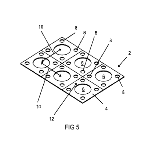
25 Fig. 5 is a view of a rectangular array of the PMUTs as shown in Fig.
2;
Fig. 6 is a view of an array of the PMUTs as shown in Fig. 2 attached to a
flexible
substrate;
Fig. 7 is a view of an unmanned aerial vehicle with the array of Fig. 6
attached
thereto;
30 Fig. 8 is a schematic diagram of a PMUT and associated system for
reducing direct
path signals;
Fig. 9 is a flowchart illustrating a method of generating an estimate of the
direct
path signals of the system shown in Figs. 8 and 9;
Fig. 10 is a further schematic diagram of a PMUT and associated system for
35 reducing direct path signals; and
CA 03155317 2022-4-20
WO 2021/079160
PCT/GB2020/052712
- 13 -
Fig. 11 is a view of a PMUT using optical receivers.
Fig. 1 is a simplified view of a piezoelectric micro-machined ultrasonic
transducer
(PMUT) 2 in accordance with an embodiment of the invention. The PM UT 2
5 comprises a square silicon die 4 onto which an ultrasonic transmitter 6
and an
ultrasonic receiver 8 are formed. Further details of the fabrication process
are
given below and with reference to Fig. 3.
As will be seen, the transmitter 6 is circular and located in the centre of
the die.
10 The receiver 6 is much smaller than the transmitter 6 and is located in
the unused
space in one corner of the die. Fig. 2 shows a variant embodiment in which
respective receivers 8 are located in each corner of the die 4. Of course
other
numbers of receivers could be provided ¨ e.g. two, three or more. They could
also
be located elsewhere or more than one could be located in a given corner. The
15 transmitter could be differently shaped or located and/or multiple
transmitters could
be provided.
The transmitter 6 might be designed, for example, to transmit signals at a
frequency
of 40 kHz or higher. The die 4 has a width of approximately 4mm which is half
of
20 the wavelength of these signals in air. The transmitter 6 has a
diameter of
approximately 3mm whereas the receiver(s) has a diameter of approximately 0.1
mm.
Fig. 3 is a schematic diagonal cross-section which shows in more detail the
layers
25 of the PMUT 2 shown in Fig. 2. This comprises a silicon substrate 100
having an
aperture 106 at its centre corresponding to the transmitter and smaller
apertures
108 in the corners corresponding to the receivers. Laid on the silicon
substrate 100
is a silicon membrane 102.
30 Above the transmitter and receiver apertures 106, 108 are respective
piezoelectric
stacks comprising a piezoelectric thin film material layer 104¨ e.g. of AIN,
AlScN or
PZT ¨ sandwiched between two electrodes 110.
The device can be fabricated by using typical microfabrication technologies.
The
35 structures for the transmitters and microphones can be typically thin
membranes,
CA 03155317 2022-4-20
WO 2021/079160
PCT/GB2020/052712
- 14 -
(one or two dimensional) cantilever structures or bridges. The main part of
these
mechanical structures typically comprises silicon. These structures can be
manufactured by e.g. silicon bulk micromachining - i.e. removal of a major
part of
the silicon when starting with a silicon wafer, which leaves the intended
mechanical
5 (thin) structure or silicon surface micromachining - Le. depositing a
(structured)
sacrificial layer and a silicon thin film leaving the mechanical structure
after
structuring the silicon film and removing the sacrificial layer.
Besides the main mechanical part of the transmitter or microphone elements,
these
10 elements include thin film metal electrodes and the piezoelectric thin
film. This
might be the same piezoelectric thin film material for the transmitter and
microphone part of the device or different piezoelectric thin film materials
with
optimized properties for transmitting and sensing. The thin-film electrode
materials
and piezoelectric thin film material(s) are typically structured prior to the
structuring
15 of the silicon part of the mechanical structure. Depending on the
actuation and
read-out concept either two electrodes ¨ one layer below and one on the top of
the
piezoelectric layer using the 31-mode ¨ or one electrode - on top of the
piezoelectric layer using the 33-mode- can be used.
20 The electrode materials are typically deposited by a sputtering
process. The
piezoelectric thin-film materials can ¨ dependent on the material ¨ also be
deposited by physical methods such as sputtering or with a pulsed-laser
deposition
process or using chemical methods such as chemical vapor deposition (CVD) or
chemical solution deposition (CSD).
Fig. 4 shows a highly simplified schematic block diagram of the typical
components
of an ultrasound transmission and reception system using the PMUTs 6, 8
described herein. The system includes a CPU 20 having a memory 22 and a
battery 24 which will typically power all components of the system. The CPU 20
is
30 connected to a signal generator 26 and a signal sampler 28. These could
be
provided in practice by a suitable digital signal processor (DSP). The signal
generator 26 is connected to a transmit amplifier 30 which drives the
ultrasonic
transmitter 6.
CA 03155317 2022-4-20
WO 2021/079160
PCT/GB2020/052712
- 15 -
On the other side the receivers 8 are connected to a receive amplifier 32
which
passes signals to the sampler 28 and onto the CPU. It will be noted that
because
the transmitter 6 is separate from the receivers 8 and the path for driving it
is
independent of the path for receiving signals, there is no need for
complicated
5 switching electronics and transmission and reception can be carried out
simultaneously.
In use the transmitter 6 can be driven with relatively long, low power signals
¨ e.g.
more than 0.1 or 0.2 milliseconds long rather than needing to be driven with a
sharp
10 burst signal.
Fig. 5 shows a rectangular array of PMUTs 2 of the type shown in Fig. 2. Here
it will
be seen that the individual dies 4 are tessellated together in a mutually
abutting
relationship on a common substrate (not shown) to form the array. Since the
dies
15 4 are a half wavelength wide, the centre-centre spacings 10 of the
transmitters 6 in
both X and Y directions are also half a wavelength. It will also be seen that
receivers 8 in respective corners of adjacent dies form respective 2x2 mini
arrays
12. Due to the size of the dies 4, these mini arrays 12 are also separated by
half a
wavelength.
Although in Fig. 5 only six dies 4 are shown, in exemplary embodiments there
might
be many dies in one or both dimensions of the array.
The wavelength A of sound depends on the velocity of sound c and its frequency
f:
25 A= cif
For technical usable ultrasound in air (above 40kHz to ensure it is above the
audible range for dogs) the wavelength is below 8.6 mm and half the
wavelength,
which is an important parameter for ultrasound arrays, is therefore below 4.3
mm.
30 This is a typical dimension of a MEMS (rnicroelectrornechanical system)
type
device such as those described herein.
For typical MEMS type structures such as cantilevers and membranes, the
frequency of the fundamental vibration modes can be expressed by the following
35 equations:
CA 03155317 2022-4-20
WO 2021/079160
PCT/GB2020/052712
- 16 -
Cantilever
= 1.015 t r
2r L2is p
Circular membrane/diaphragm:
40.8t
f 2ir dz
j12(1 ¨ p
5 Here t is the thickness of the mechanical structure, E the Young's
modulus, p is the
density, L the length of a cantilever and d the diameter of a circular
membrane.
These equations are for a single material, but can quite easily be modified
for a
multi-layered structure.
10 These equations exemplify the feasibility of MEMS ultrasound
structures. The
eigenfrequency of a 8 pm thick silicon membrane with 1250pm diameter, which
are
typical dimensions for MEMS structures, has an eigenfrequency of about 80kHz.
Most standard beamforming algorithms benefit from A/2 spacing because it means
15 that each incoming wave front can be discerned from other incoming
wavefronts
with a different angle or wavenumber, which in turn means that the problem of
so-
called 'grating lobes' is prevented. Classical beamforming methods that
benefit from
A/2 (or tighter) spacing include (weighted) delay-and-sum beamformers,
adaptive
beamformers such as MVDR/Capon, direction-finding methods like MUSIC and
20 ESPRIT and Blind Source Estimation approaches like DUET, as well as
wireless
communication method, ultrasonic imaging methods with additional constraint
such as
entropy or information maximization.
Fig. 6 shows a further array 14 made up of a number of dies 4 of the type
shown in
25 Fig. 2 attached to a flexible substrate in the form of a ribbon 16
made, for example,
of polyurethane. This array 14 can be attached to any number of objects or
devices
or could form part of a wearable device. Fig. 7 shows one example where the
array
14 is attached to the body of an unmanned aerial vehicle or drone 18. In such
an
arrangement a processor (not shown) driving the transmitters and receivers
thereof
30 can be programmed to operate in a calibration phase whereby individual
transmitters 6 in the array 14 transmit different signals, or signals at
different times,
which are them received by receivers 8 on other dies in the array. Using a
suitable
algorithm, such as transmitting a coded signal (CDMA type) or a chirp signal,
CA 03155317 2022-4-20
WO 2021/079160
PCT/GB2020/052712
- 17 -
followed by matched filtering or deconvolution, and signal peak detection such
as
i.e. a CFAR filter, the times of flight of such transmissions can be used to
establish
the relative mutual positions of the individual dies 4. In some situations one
is more
interested in computing relative time-differences of arrival (TDOA) between
two
5 receivers and one transmitted/reflected signal. There is a range of
popular methods
for this, including Generalized Cross Correlation PHAse Transform (GCC-PHAT)
and Steered Response PHAse Transform (SRP-PHAT).
These can then be used during operation to apply appropriate phase differences
to
10 the signals of respective receivers to allow them to act as a coherent
array ¨ e.g. for
beamfornning. Such an approach is beneficial in allowing the array to be
attached
to any number of irregularly shaped objects so that the precise attachment is
not
critical.
15 The drone 18 can use the array 14 for echolocation, collision avoidance
etc.
Fig. 8 is a schematic diagram of a PMUT 302 and associated system which is
able
to compensate for direct path signals. The system includes a PMUT 302 which
comprises a square silicon die 304 on which a transmitter element 306, and a
20 receiver element 308 are formed.
An ASIC (application-specific integrated circuit) or DSP (digital signal
processor) 42
is connected to a primary digital to analogue (D/A) converter 34. This primary
D/A
converter 34 is connected to an amplifier 132 which drives the ultrasonic
transmitter
25 306. The ultrasonic transmitter 306 thus emits an ultrasonic signal 48.
The ultrasonic receiver 308 receives reflected echoes 50 which are reflected
from
an object of interest. The ultrasonic receiver 308 also receives acoustic
direct path
signals 44, 46. One of the direct path signals 44 is an in-air direct acoustic
path
30 signal. The other direct path signal 46 is transmitted through the body
of the die 304
from the transmitter 306 to the receiver 308. Other transmission mechanisms
may
contribute to the overall direct path signal received by the receiver 308.
The ASIC/DSP 42 further generates an estimate of the effect of the direct path
35 signals 44, 46 on the received ultrasonic signals as will be described
in more detail
CA 03155317 2022-4-20
WO 2021/079160
PCT/GB2020/052712
- 18 -
below with reference to Fig. 9. The ASIC/DSP 42 comprises a signal modifier 52
which may modify the estimate produced. The signal modifier 52 may for example
incorporate a filter that applies a convolution to the output signal from the
ASIC/DSP 42. The estimated direct path signal passes to a D/A converter 54
which
5 converts it to an analogue signal. This analogue signal passes through
an amplifier
36 to a mixer 38. The mixer subtracts the analogue estimated direct path
signal
from the analogue signal produced by the receiver 308, and the resultant
signal is
passed to an analogue to digital (ND) converter 40 to produce a digital signal
which
may be further analysed e.g. for echolocation, stored etc.
Typically, the direct path signals 44, 46 are much stronger than the received
echoes
50. The described embodiment advantageously removes the direct path signals
44,
46 prior to sampling for conversion to digital signals. If the direct path
signals 44, 46
were not removed, the AID converter 40 would require a high dynamic range in
15 order to convert both the received echoes 50 to digital signals, as
well as the direct
path signals 44, 46. A high dynamic range AID converter is more complex and
thus
more expensive and power consuming.
Fig. 9 is a flowchart illustrating a method generating the estimate of the
direct path
20 signals 44, 46 in the system shown in Fig. 8. At step 58, the system
starts recording
the direct path signals 44, 46 from the transmitter element 306 to an
individual
receiver 308. If there are multiple receivers, as shown in Fig. 2, then the
process
may be repeated for each individual receiver. The signal recorded does not
include
reflections from the environment because time-gating is used to exclude these
25 (since they have a longer time of flight than the direct path signals).
Since the direct path signals 44, 46 can vary with conditions, such as
temperature,
it may be desirable to record several direct path signals 44, 46 over a longer
period
of time, or over multiple time instances during a day (when the system is not
in use)
30 to obtain a sufficient database in step 60. Optionally, the recordings
may be used to
estimate the direct path signals 44, 46 at different temperatures and pressure
levels
by resampling at slightly higher or lower frequencies.
At step 62, a criterion for whether a sufficient database of direct path
signals has
35 been created is tested. This criterion could be related to any suitable
quality
CA 03155317 2022-4-20
WO 2021/079160
PCT/GB2020/052712
- 19 -
parameter such as the degree of self-repetition of the pre-recorded direct
path
signals i.e. whether the past signals are repeating themselves, or the
criterion could
be tied to a temperature sensor which requires direct path signals for a
certain
range of temperatures to have been collected for the database to be
"complete".
5 The database may be updated from time to time as the physical
surroundings
around the elements may change. For example, the transmitter 306, or receiver
308
may be moved to a different housing, or dust may have fallen on or close to
the
sensor and affect the direct acoustic paths. If the database quality is not
adequate,
then further recording of the direct path signals is carried out
Once the database quality is determined to be adequate, in step 64, a
recording
session for reflected signals begins. An initial estimate of direct path
signals is
provided in step 66, either as a random guess, or taking into account input
from a
temperature sensor (not shown) used in the direct path signal database
creation
15 steps 58-62. The D/A converter 54 then converts the estimated direct
path signal
from the ASIC/DSP 42 so that it can be subtracted in the mixer 38.
In step 70, the transmitter 306 transmits an ultrasound signal, and the
receiver 308
receives the reflected echoes 50, and direct path signals 44, 46. In steps 72
and 74,
20 the quality of the received data is monitored to identify whether the
selected direct
path signal from step 66 was a good selection. An example of a parameter for
quality is minimal energy which signals that the strongest component in the
received signal (the direct path 44, 46) has been successfully been removed.
Alternatively, maximum sparsity may be used as a parameter, as this signals
that a
25 "clear echo" is being received. Generally, mixes of echoes 50 and
direct path
signals 44, 46 tend to be more complex than any one of them separately. Other
parameters such as reflecting entropy or self-similarity over time could also
be
used.
30 If the quality in step 74 is good, in step 76, the received signal from
the mixer 38
passes to the A/D converter 40, and may be used for further analysis such as
proximity, presence or gesture sensing.
If the quality in step 74 is poor, and the quality is not below a first
threshold in step
35 78, only minor modifications to the estimate of the direct path signal
are necessary.
CA 03155317 2022-4-20
WO 2021/079160
PCT/GB2020/052712
- 20 -
These minor modifications may be incorporated by a filter 52 which applies a
convolution to the estimated direct path signal in order to attempt to rectify
the
estimated direct path signal in step 80.
5 If the quality parameter is below a second critical threshold, in step
82, the system
starts to record direct path signals again, in order to build up a new
database. This
may be necessary when there is a substantial change in the behaviour or
surroundings of the transmitter element 306.
10 If the quality parameter is below the first threshold, but not below
the second
threshold, another candidate may be selected for the estimated direct path
signal,
as shown in step 84.
Fig. 10 is a schematic diagram of another embodiment of a PMUT 302' and
15 associated system for compensating for direct path signals. This
embodiment is
almost identical to that of Fig. 8 and similar parts are indicated with
similar
reference numerals with the addition of a prime symbol. However in this
embodiment the PMUT 302' further includes acoustic path bafflers 56. These
acoustic path barriers 56 may for example, be a cylinder around the
transmitter
20 306', a cylinder around the receiver 308', or a cylinder around both
the transmitter
306' and receiver 308'. The acoustic path barriers 56 act to physically reduce
the
strength of the in-air direct acoustic path signal 44' by reducing air
transmission of
the signal 44' between the transmitter 306' and the receiver 308'.
25 Fig. 11 is a view of a PMUT 402 using optical receivers 408. These
could, for
example comprises MEMS structures where movement of a membrane by acoustic
signals is read out using light reflected from the membrane, e.g. using a
diffraction
grating. The optical receivers 408 may be much more closely spaced than the
receivers 8 shown in Fig. 2, as optical receivers have much lower self-noise
and
30 thus much better SNR than conventional receivers. The optical receivers
408 may
therefore be much more closely spaced than ht2, with images still obtained
with
high resolution. As such, through use of closely spaced optical receivers 408,
a
compact ultrasound imaging component is formed on a single die 404.
CA 03155317 2022-4-20