Note: Descriptions are shown in the official language in which they were submitted.
WO 2021/081650
PCT/CA2020/051456
ALIGNMENT DEVICE FOR ALIGNING TRANSMITTER AND RECEIVER OF WIRELESS
POWER TRANSFER SYSTEM, AND METHOD THEREFOR
Field
[0001] The subject disclosure relates generally to wireless power transfer and
in particular, to an
alignment device for aligning a transmitter and receiver of a wireless power
transfer system, and
a method therefor.
Background
[0002] Wireless charging and wireless power transfer systems are becoming an
increasingly
important technology to enable the next generation of devices. The potential
benefits and
advantages offered by the technology is evident by the increasing number of
manufacturers and
companies investing in the technology.
[0003] A variety of wireless power transfer systems are known. A typical
wireless power transfer
system includes a power source electrically connected to a wireless power
transmitter, and a
wireless power receiver electrically connected to a load.
[0004] In magnetic induction systems, the transmitter has a coil with a
certain inductance that
transfers electrical energy from the power source to a receiving coil with a
certain inductance.
Power transfer occurs due to coupling of magnetic fields between the inductors
of the transmitter
and receiver. The range of these magnetic induction systems is limited, and
the inductors of the
transmitter and receiver must be tightly coupled, i.e. have a coupling factor
above 0.5 and be in
optimal alignment for efficient power transfer.
[0005] There also exist resonant magnetic systems in which power is
transferred due to coupling
of magnetic fields between the inductors of the transmitter and receiver. The
transmitter and
receiver inductors are loosely coupled, i.e. have a coupling factor below 0.5.
In resonant magnetic
systems the inductors are resonated using at least one capacitor. In resonant
magnetic systems,
the transmitter is self-resonant and the receiver is self-resonant The range
of power transfer in
resonant magnetic systems is increased over that of magnetic induction systems
and alignment
issues are rectified. While electromagnetic energy is produced in magnetic
induction and resonant
magnetic systems, the majority of power transfer occurs via the magnetic
field. Little, if any, power
is transferred via electric capacitive or resonant electric capacitive
(electric fields).
[0006] The Qi wireless charging standard is an exemplary implementation of a
magnetic induction
system. The Qi wireless charging standard is used in low power consumer
electronics such as
smart phones and wearable devices. Furthermore, low cost power converters,
coils and
CA 03156585 2022-4-28
WO 2021/081650
PCT/CA2020/051456
integrated circuits are available for use in the Qi wireless charging
standard. The Qi wireless
charging standard operates in the kHz frequency range. Accordingly, devices
operating according
to the Qi wireless charging standard have limited coupling range, require
precise coil alignment
and use ferrite-based coils, which can be heavy and fragile. Consequently, the
application scope
of the Qi wireless charging standard is limited.
[0007] In electrical capacitive systems, the transmitter and receiver have
capacitive electrodes.
Power transfer occurs due to coupling of electric fields between the
capacitive electrodes of the
transmitter and receiver_ Similar, to resonant magnetic systems, there exist
resonant electric
systems in which the capacitive electrodes of the transmitter and receiver are
made resonant
using at least one inductor. In resonant electric systems, the transmitter is
self-resonant and the
receiver is self-resonant Resonant electric systems have an increased range of
power transfer
compared to that of electric capacitive systems and alignment issues are
rectified While
electromagnetic energy is produced in electric capacitive and resonant
electric systems, the
majority of power transfer occurs via the electric field. Little, if any,
power is transferred via
magnetic induction or resonant magnetic induction.
[0008] Although wireless power transfer techniques are known, improvements are
desired.
Summary
[0009] It should be appreciated that this Summary is provided to introduce a
selection of concepts
in a simplified form that are further described below in the Detailed
Description of Embodiments.
This Summary is not intended to be used to limit the scope of the claimed
subject matter.
[0010] Accordingly, in one aspect there is provided an alignment device
comprising: a coil
configured to generate an induced voltage from a magnetic field, or an
electrode configured to
generate an induced voltage from an electric field; and a comparator
configured to compare the
induced voltage to a threshold voltage and activate an indicator based on the
comparison.
[0011] In one or more embodiments, the induced voltage is proportional to the
strength of the
magnetic field intersecting the coil, or to the electric field intersecting
the electrode.
[0012] In one or more embodiments, the alignment device is configured to align
a transmitter and
a receiver for optimal power transfer efficiency.
[0013] In one or more embodiments, the alignment device is configured to align
a transmitter coil
and a receiver coil for optimal power transfer efficiency.
[0014] In one or more embodiments, the alignment device is configured for use
with a high
frequency wireless power transfer system.
2
CA 03156585 2022-4-28
WO 2021/081650
PCT/CA2020/051456
[0015] In one or more embodiments, the coil or electrode forms part of a field
detection unit
(FDU).
[0016] In one or more embodiments, the FDU comprises at least one tuning
capacitor configured
to tune the coil.
[0017] In one or more embodiments, the FDU comprises a rectifier configured to
rectify the
induced voltage from alternating current (AC) to direct current (DC).
[0018] In one or more embodiments, the FDU comprises at least one diode
configured to add
capacitors to the coil to decrease a resonant frequency of the coil
[0019] In one or more embodiments, the alignment device comprises a plurality
of FDUs, each
FDU comprising an individual coil configured to generate an induced voltage
from a magnetic
field, or an individual electrode configured to generate an induced voltage
from an electric field.
[0020] In one or more embodiments, the alignment device comprises four FDUs
orthogonally
positioned with respect to each other in a plane.
[0021] In one or more embodiments, the FDUs are positioned equidistant to each
other in the
plane.
[0022] In one or more embodiments, the alignment device comprises five FDUs
orthogonally
positioned with respect to each other in a plane.
[0023] In one or more embodiments, four FDUs are positioned equidistant to a
central FDU in the
plane.
[0024] In one or more embodiments, each FDU is associated with an individual
indicator.
[0025] In one or more embodiments, the comparator forms part of a main board.
[0026] In one or more embodiments, the main board further comprises the
indicator.
[00271 In one or more embodiments, the main board further comprises a voltage
divider
configured to scale down voltage.
[0028] In one or more embodiments, the main board further comprises a
sensitivity control
configured to control the threshold voltage.
[0029] In one or more embodiments, the alignment device further comprises a
spirit level.
[0030] According to another aspect there is provided an alignment device for
determining an
optimal alignment of a transmitter and a receiver configured to extract power
from the transmitter
via magnetic field coupling or electric field coupling.
[0031] In one or more embodiments, the alignment device comprises a coil
configured to
generate an induced voltage from a magnetic field.
[0032] In one or more embodiments, the alignment device comprises an electrode
configured to
generate an induced voltage from an electric field.
3
CA 03156585 2022-4-28
WO 2021/081650
PCT/CA2020/051456
[0033] In one or more embodiments, the alignment device comprises an indicator
configured to
activate based on a comparison between the induced voltage and a threshold
voltage.
[0034] In one or more embodiments, the alignment device further comprises a
comparator
configured to compare the induced voltage to the threshold voltage.
[0035] In one or more embodiments, the alignment device comprises any of the
features or
elements of the described alignment devices.
[0036] According to another aspect there is provided, a method comprising:
a) activating a transmitter positioned on one side of a material;
b) positioning an alignment device on another side of the material opposite
the transmitter
c) generating, via a coil of the alignment device, an induced voltage from
a magnetic field
generated by the transmitter, or generating, via an electrode of the alignment
device, an induced
voltage from an electric field generated by the transmitter;
d) activating an indicator of the alignment device based on a comparison of
the induced
voltage with a threshold voltage;
e) repositioning the alignment device relative to the transmitter; and
repeating steps c) to e) until optimal power transfer efficiency between the
transmitter and
the alignment device is obtained.
[0037] In one or more embodiments, the method further comprises positioning a
receiver at a
position at which optimal power transfer efficiency between the transmitter
and the alignment
device is obtained.
[0038] In one or more embodiments, the alignment device of the method
comprises any of the
described alignment devices.
Brief Description of the Drawinos
[0039] Embodiments will now be described more fully with reference to the
accompanying
drawings in which:
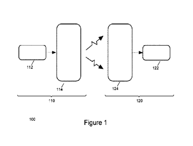
[0040] Figure 1 is a block diagram of a wireless power transfer system;
[0041] Figure 2 is a block diagram of a transmitter and receiver of a high
frequency wireless
power transfer system mounted to a material;
[0042] Figure 3 is block diagram of an alignment device in accordance with an
aspect of the
subject disclosure;
[0043] Figure 4 is a partial schematic layout of a field detection unit (FDU)
of the alignment device
of Figure 3;
[0044] Figure 5 is a plan view of a coil of the FDU of Figure 4;
4
CA 03156585 2022-4-28
WO 2021/081650
PCT/CA2020/051456
[0045] Figure 6 is a partial schematic layout of the FDU of Figure 4 with an
alternating magnetic
field present during operation;
[0046] Figure 7 is a partial block diagram of another embodiment of the
alignment device of
Figure 3;
[0047] Figure 8 is partial block diagram of another embodiment of the
alignment device of Figure
3;
[0048] Figure 9 is a magnetic field density plot generated by the transmitter
of the high frequency
wireless power transfer system of Figure 2;
[0049] Figure 10 is a plan view of the magnetic field density plot of Figure 9
with the alignment
device of Figure 8;
[0050] Figure 11 is another plan view of the magnetic field density plot of
Figure 9 with the
alignment device of Figure 8 during operation;
[0051] Figure 12 is another plan view of the magnetic field density plot of
Figure 9 with the
alignment device of Figure 8 during operation;
[0052] Figure 13 is another plan view of the magnetic field density plot of
Figure 9 with the
alignment device of Figure 8;
[0053] Figure 14 is another plan view of the magnetic field density plot of
Figure 9 with the
alignment device of Figure 8 during operation;
[0054] Figure 15 is a partial schematic layout of another FDU of the alignment
device of Figure
3;
[0055] Figure 16 is a partial schematic layout of another FDU of the alignment
device of Figure
3;
[0056] Figure 17 is a partial block diagram of another embodiment of the
alignment device of
Figure 3;
[0057] Figure 18 is a proximity diagram indicating regions of proximity of an
alignment device to
an optimal alignment;
[0058] Figure 19 is a block diagram of another embodiment of the alignment
device of Figure 3;
and
[0059] Figures 20A-20C are spatial distribution diagrams of detected magnetic
fields.
Detailed Description of Embodiments
[0060] The foregoing summary, as well as the following detailed description of
certain examples
will be better understood when read in conjunction with the appended drawings.
As used herein,
an element or feature introduced in the singular and preceded by the word "a'
or "an" should be
CA 03156585 2022-4-28
WO 2021/081650
PCT/CA2020/051456
understood as not necessarily excluding the plural of the elements or
features. Further, references
to "one example" or "one embodiment" are not intended to be interpreted as
excluding the
existence of additional examples or embodiments that also incorporate the
described elements
or features. Moreover, unless explicitly stated to the contrary, examples or
embodiments
"comprising" or "having" or "including" an element or feature or a plurality
of elements or features
having a particular property may include additional elements or features not
having that property.
Also, it will be appreciated that the terms "comprises", "has", Includes"
means "including by not
limited to" and the terms "comprising", "having" and "including" have
equivalent meanings. It will
also be appreciated that like reference characters will be used to refer to
like elements throughout
the description and drawing&
[0061] As used herein, the terms "adapted" and "configured" mean that the
element, component,
or other subject matter is designed and/or intended to perform a given
function. Thus, the use of
the terms "adapted" and "configured" should not be construed to mean that a
given element,
component, or other subject matter is simply "capable of" performing a given
function but that the
element component, and/or other subject matter is specifically selected,
created, implemented,
utilized, and/or designed for the purpose of performing the function. It is
also within the scope of
the subject disclosure that elements, components, and/or other subject matter
that are described
as being adapted to perform a particular function may additionally or
alternatively be described
as being configured to perform that function, and vice versa. Similarly,
subject matter that is
described as being configured to perform a particular function may
additionally or alternatively be
described as being operative to perform that function.
[0062] It will be understood that when an element is referred to as being
"on," "attached" to,
"connected" to, "coupled" with, "contacting," etc., another element, it can be
directly on, attached
to, connected to, coupled with or contacting the other element or intervening
elements may also
be present
[0063] It should be understood that use of the word "exemplary", unless
otherwise stated, means
by way of example' or 'one example', rather than meaning a preferred or
optimal design or
implementation.
[0064] Unless defined otherwise, all technical and scientific terms used
herein have the same
meaning as is commonly understood by one of skill in the art to which the
subject disclosure
pertains.
[0065] As used herein, the terms "approximately", "about", "approximately",
"generally" etc.
represent an amount or condition close to the stated amount or condition that
still performs the
desired function or achieves the desired result. For example, the terms
"approximately",
6
CA 03156585 2022-4-28
WO 2021/081650
PCT/CA2020/051456
"about", "approximately", "generally" etc. may refer to an amount or condition
that is within
engineering tolerances that would be readily appreciated by a person skilled
in the art.
[0066] Turning now to Figure 1, a wireless power transfer system generally
identified by reference
numeral 100 is shown. The wireless power transfer system 100 comprises a
transmitter 110
comprising a power source 112 electrically connected to a transmit element
114, and a receiver
120 comprising a receive element 124 electrically connected to a load 122.
Power is transferred
from the power source 112 to the transmit element 114. The power is then
transferred from the
transmit element 114 to the receive element 124 via resonant or non-resonant
electric or magnetic
field coupling. The power is then transferred from the receive element 124 to
the load 122.
Exemplary wireless power transfer systems 100 include a high frequency
inductive wireless
power transfer system as described in U.S. Patent Application No. 17/018,328,
the relevant
portions of which are incorporated herein.
[0067] Turning now to Figure 2, another exemplary wireless power transfer
system is shown. In
this embodiment, the wireless power transfer system is a high frequency
wireless power transfer
system 200 as described in the above-incorporated '328 application. In this
embodiment, the high
frequency wireless power transfer system 200 is an inductive system. One of
reasonable skill in
the art will appreciate that the high frequency wireless power transfer system
200 may be
configured to transfer power via high frequency magnetic inductive cowling or
high frequency
electric capacitive coupling. In magnetic inductive coupling systems, the
majority of power transfer
occurs via the magnetic field. Little, if any, power is transferred via
electric capacitive or resonant
electric capacitive (electric fields). In electric capacitive coupling
systems, the majority of power
transfer occurs via the electric field. Little, if any, power is transferred
via magnetic inductive or
resonant magnetic induction.
[0068] In this embodiment, the high frequency wireless power transfer system
200 is configured
to transfer power via high frequency magnetic field coupling. The high
frequency wireless power
transfer system 200 comprises a transmitter 210 configured to operate at a
given frequency, and
a receiver 220 configured to operate at the operational frequency of the
transmitter 210. As shown
in Figure 2, the transmitter 210 is positioned on a material 230. The material
230 is fabricated
from any type of suitable material or material combination that is not
conductive or magnetic, e.g.
wood, glass, stone, brick, concrete, plastic, except for materials or a
combination of materials that
would cause termination of the fields prematurely, i.e. act as a shield. In
this embodiment, the
material 230 forms part of a wall. The receiver 220 is positioned on the
opposite side of the
material 230, such that the material 230 is directly between the transmitter
210 and receiver 220.
7
CA 03156585 2022-4-28
WO 2021/081650
PCT/CA2020/051456
One of reasonable skill in the art will recognize that more than one
transmitter 210 and receiver
220 is possible.
[0069] In this embodiment, the transmitter 210 comprises a transmitter coil
212, and the receiver
220 comprises a receiver coil 222. One of skill in the art will recognize that
more than one
transmitter coil 212 and receiver coil 222 is possible.
[0070] The transmitter 210 operates in current-mode output (constant current
output). In current-
mode output, the transmitter 210 is configured to generate a magnetic field
without the
requirement for a receiver 220 to be present near the transmitter 210.
[0071] Generally, current-mode output high frequency wireless power transfer
systems differ from
voltage-mode output (constant voltage output) high frequency wireless power
transfer systems in
that voltage-mode output transmitters 210 cannot generate and maintain a
magnetic field without
a receiver 220 present near the transmitter 210. If a receiver 220 is not
present in a voltage-mode
output high frequency wireless power transfer system, the transmitter 210 will
essentially operate
in a short-circuit condition, and therefore cannot sustain generation of a
magnetic field.
[0072] Power transfer from transmitter 210 to receiver 220 occurs through the
material 230. In
order to maximize the coupling coefficient value and the highest power
transfer efficiency, the
transmitter 210 and receiver 220 should be optimally aligned. If the material
230 is opaque or if it
completely obstructs view of the position of either the transmitter 210 or
receiver 220, or both, it
may be problematic to optimally align the transmitter 210 and receiver 220.
[0073] In optimal alignment of the receiver 220 with the transmitter 210, the
receiver coil 222 is
in optimal alignment with the transmitter coil 212.
[0074] Turning now to Figure 3, a block diagram of an alignment device 300 in
accordance with
an aspect of the subject disclosure is shown. Given a certain fixed distance
away from the
transmitter 210, the alignment device 300 determines the position at which,
when a receiver 220
is installed, the transmitter 210 and receiver 220 will be in optimal
alignment to achieve the
maximum coupling coefficient value and hence, the highest power transfer
efficiency. The
transmitter coil 212 and receiver coil 222 are in optimal alignment when their
centre axes normal
to the transmitter coil 212 and the receiver coil 222 are collinear. The
centre axis of each of the
transmitter coil 212 and the receiver coil 222 is the axis extending through
the centre of mass of
the respective coil 212 and 222.
[0075] In particular, the alignment device 300 is configured to generate an
induced voltage from
a magnetic field generated by the transmitter 210. Specifically, the alignment
device 300 is
configured to generate an induced alternating voltage when intersected by the
alternating
magnetic field generated by the transmitter 210. Based on the induced
alternating voltage, the
8
CA 03156585 2022-4-28
WO 2021/081650
PCT/CA2020/051456
alignment device 300 is configured to determine the position of the alignment
device 300 in
relation to the transmitter 210 or transmitter coil 212. The receiver 220 and
receiver coil 222 may
then be positioned in the position in which power transfer efficiency is
maximized between the
transmitter and receiver coils 212 and 222 as determined by the alignment
device 300.
[0076] The alignment device 300 comprises a field detection unit (FDU) 310 and
a main board
318. The FDU 310 comprises at least one coil 312, at least one tuning
capacitor 314 and a rectifier
318. The coil 312 is electrically connected to the tuning capacitor 314. The
tuning capacitor 314
is electrically connected to the coil 312 and the rectifier 316. The FDU 310
is electrically connected
to the main board 318. Specifically, the rectifier 316 of the FDU 310 is
electrically connected to a
voltage divider 320 of the main board 318. The main board 318 comprises the
voltage divider
320, a comparator, which in this embodiment takes the form of a comparator
circuit 322, a
sensitivity control 323 and an indicator 324. The voltage divider 320 is
electrically connected to
the rectifier 316 of the FDU 310. The voltage divider 320 is also electrically
connected to the
comparator circuit 322. The comparator circuit 322 is electrically connected
to the indicator 324
via a driving circuit (not shown). The indicator 324 is electrically connected
to the comparator
circuit 322 via a driving circuit (not shown).
[0077] The comparator circuit 322 is configured to compare a voltage signal of
the rectifier 316
against a preset threshold voltage. In this embodiment, the indicator 324
associated with the FDU
310 is a light emitting diode (LED). The LED is driven by an LED driving
circuit (not shown). The
LED driving circuit, which, in this embodiment, comprises a transistor (not
shown), is triggered by
output from the comparator circuit 322. The sensitivity control 323 is
electrically connected to the
comparator circuit 322. The sensitivity control 323 is configured to adjust
and set a threshold
voltage. In this embodiment, the sensitivity control 323 is a turnable knob,
dial or the like.
[0078] The indicator 324 assists in determining the optimal alignment position
at which the
maximum coupling coefficient and the highest wireless power transfer
efficiency is achieved_ For
example, the indicator 324 comprises a visual indicator, including, but not
limited to, an LED or
other type of light/diode; an audible indicator; any type of sensory
indicator, including but not
limited to, vibration; and any combination of available types of indicators
324, not limited to the
types of indicators described herein.
[0079] One of reasonable skill in the art will recognize that multiple FDUs
310 may be attached
to a single main board 318. Furthermore, one of reasonable skill in the art
will appreciate that
multiple indicators 324 on a single main board 318 are also possible. For
example, one indicator
324 for each FDU 310 may be provided.
9
CA 03156585 2022-4-28
WO 2021/081650
PCT/CA2020/051456
[0080] In this embodiment, the alignment device 300 is configured for use with
the high frequency
inductive wireless power transfer system as described in the above-
incorporated '328 application.
In this embodiment, the alignment device 300 is configured to operate with the
current-mode
output transmitter 210, both independent from, and in the absence of the
receiver 220.
[0081] In a voltage-mode output high frequency wireless power transfer system,
the alignment
device 300 cannot be used without the receiver 220 present Accordingly, in
voltage-mode output
high frequency wireless power transfer systems, the alignment device 300 is
integrated into the
receiver 220. Conversely, the current-mode output high frequency wireless
power transfer system
200 will allow the alignment device 300 to operate while being physically
separate from the
receiver 220, (Le. decoupled, from the receiver 220), and therefore, allowing
the alignment device
300 to operate independently with the transmitter 210, in the complete absence
of the receiver
220. As one of reasonable skill in the art will appreciate, the alignment
device 300 may
alternatively be integrated into the receiver 220 of a current-mode output
high frequency wireless
power transfer system.
[0082] Turning now to Figure 4, the FDU 310 of the alignment device 300 is
further illustrated. As
previously stated, the FDU 310 comprises at least one coil 312. The coil 312
is electrically
connected in series to tuning capacitors 314. The tuning capacitors 314 are
electrically connected
to the coil 312 and to the rectifier 316. The combination of the electrically
connected coil 312,
tuning capacitors 314 and rectifier 316 forms the FDU 310. The FDU 310 is
electrically connected
to the main board 318. In this embodiment, the alignment device 300 comprises
a single FDU
310. In another embodiment the alignment device 300 comprises multiple FDUs
310, for
example, four FDUs 310. Each FDU 310 is identical.
[0083] Turning now to Figure 5, the coil 312 is further illustrated. In this
embodiment, the coil 312
is implemented on a printed circuit board (PCB) made of FR4 PCB material. In
this embodiment,
the coil 312 is a planar coil consisting of multiple turns and is in the
approximate shape of a
square. In this embodiment, the total number of turns of the coil 312 is four,
each turn is 1mm
thick, and the spacing between each turn is 0.3mm. One of reasonable skill in
the art will recognize
that the coil 312 could be any other shape, such as, but not limited to,
spiral, circular, hexagonal
or octagonal. One of reasonable skill in the art will also recognize that the
number of turns, the
turn thickness and the spacing between the turns could be any suitable value.
In this embodiment,
the coil 312 has an outer width and height, 01, which is 39 mm, and inner
width and height, 02,
which is 29.5 mm. One of reasonable skill in the art will recognize that the
dimensions D1 and 02
of the coil 312 could be any suitable value. In this embodiment, the
inductance (L) of the coil 312
is 1.2 uH. One of reasonable skill in the art will recognize that the
inductance of the coil 312 is
CA 03156585 2022-4-28
WO 2021/081650
PCT/CA2020/051456
exemplary. The inductance may be as high as 6 to 8 uH. Generally, the
inductance of the coil 312
is bound by the resonant frequency of the transmitter coil 212. Increasing the
inductance of the
coil 312 will decrease the self-resonant frequency of the coil 312 such that
the self-resonant
frequency of the coil 312 approaches the resonant frequency, which may be
problematic. A higher
inductance may however, provide higher sensitivity and field detection during
operation of the
alignment device 300.
[0084] The optimal placement of the alignment device 300 coincides with the
optimal alignment
of the receiver 220 in relation to the transmitter 210. Optimal alignment of
the transmitter 210 and
the receiver 220 coincides with optimal alignment of the transmitter coil 212
and the receiver coil
222. Optimal alignment of the transmitter coil 212 and the receiver coil 222
is the position at which
the maximum coupling coefficient value and the highest wireless power transfer
efficiency is
achieved.
[0085] During operation, the transmitter 210 of the wireless power transfer
system 200 is
activated and powered on. The transmitter coil 212 generates a constant
alternating current (AC)
magnetic field. The receiver 220 can be aligned with the transmitter 210 to
allow for power to be
transferred wirelessly from the transmitter coil 212 to the receiver coil 222.
For alignment to be
optimal between the transmitter 210 and the receiver 220, the transmitter coil
and 212 the receiver
coil 222 must be in optimal alignment. Coupling and power transfer can still
occur without optimal
alignment of the transmitter coil 202 and receiver coil 212; however, the
performance of the
wireless power transfer system 200 will be degraded.
[0086] As previously stated, given a certain fixed distance away from the
transmitter 210, the
alignment device 300 determines the position at which, when the receiver 220
is installed, the
transmitter 210 and receiver 220 will be in optimal alignment to achieve the
maximum coupling
coefficient value and hence, the highest power transfer efficiency. The
transmitter coil 212 and
receiver coil 222 are in optimal alignment when their centre axes normal to
the transmitter coil
212 and the receiver coil 222 are collinear. In other words, the transmitter
coil 212 and receiver
coil 222 are in optimal alignment when the axis extending through the centre
of mass of the
respective coil 212 and 222 are collinear.
[0087] During operation of the alignment device 300, the coil 312 is
intersected by an AC
magnetic field generated by the transmitter coil 212. The coil 312 generates
an induced
alternating voltage from the AC magnetic field. The induced voltage is used to
determine the
position of the alignment device 300 in relation to the transmitter 210 of the
high frequency
wireless power transfer system 200 that operates at constant-current mode in
the transmitter coil
212.
11
CA 03156585 2022-4-28
WO 2021/081650
PCT/CA2020/051456
[0088] Specifically, the tuning capacitors 314 of the FDU 310 tune the coil
312 to the resonant
frequency of the transmitter coil 212 to generate an induced voltage from the
AC magnetic field.
The coil 312 induces an alternating voltage from the AC magnetic field and
outputs an AC voltage
signal. The induced alternating voltage is proportional to the strength of the
AC magnetic field.
The AC voltage signal is passed from the coil 312 to the rectifier 316. The
rectifier 316 rectifies
the voltage signal from AC to DC. The DC voltage signal is then passed to the
main board 318.
The voltage divider 320 scales down the DC voltage signal such that the DC
voltage signal is
compatible with the logic levels of the main board 318. In this embodiment,
the scale down factor
of the voltage divider 320 is 10. However, one of reasonable skill in the art
will recognize that the
scale-down factor could be any other suitable value depending on the design of
the main board
318. Specifically, the voltage divider 320 scales down the DC voltage so that
the DC voltage
signal may be compared by the comparator circuit 322. The scaled down DC
voltage is measured
by the comparator circuit 322. The comparator circuit 322 compares the scaled
down DC voltage
to the preset threshold voltage as provided by the sensitivity control 323.
When the voltage is
highest, (i.e. exceeds the threshold set by the sensitivity control 323 in the
comparator circuit
322), optimal alignment (or near-optimal alignment) is achieved. The
comparator circuit 322
passes the results of the comparison to the indicator 324. The scaled down DC
voltage / preset
threshold voltage comparison determines to switch on the indicator 324 or not.
Specifically, the
comparison determines whether the LED of the indicator 324 is switched on or
not. The indicator
324 indicates whether optimal alignment has been achieved.
[0089] The alignment device 300 allows for the transmitter 210 and receiver
220 to be located on
opposite sides of material 230, such as a wall or window. The alignment device
300 allows the
optimal position of the transmitter coil 212 and receiver coil 222 to be
determined, and therefore
achieves the maximum coupling coefficient value and the highest wireless power
transfer
efficiency through the material 230.
[0090] As shown in Figure 6, during operation of the alignment device 300, the
coil 312 is
subjected to an AC magnetic field in the direction indicated by arrows A. When
subjected to the
AC magnetic field, the coil 312 is intersected by the alternating magnetic
field. The AC magnetic
field that intersects the coil 312 induces an alternating voltage in the coil
312. Figure 6 shows an
example of the direction of the magnetic field lines in relation to the coil
312.
[0091] Although a particular configuration of the alignment device 300 has
been described, one
of reasonable skill in the art will appreciate that other configurations are
possible. Turning now to
Figure 7, another embodiment of an alignment device generally identified by
reference numeral
700 is shown. The alignment device 700 comprises all of the elements of the
previously described
12
CA 03156585 2022-4-28
WO 2021/081650
PCT/CA2020/051456
alignment device 300 unless otherwise stated. The alignment device 700
functions similarly to
the previously described alignment device 300 unless otherwise stated. The
alignment device
700 comprises three FDUs 710, each comprising a coil 712, at least one tuning
capacitor 714 and
a rectifier 716. The three FDUs 710 are coplanar and are arranged in an
equilateral formation.
Each FDU 710 is electrically connected to the main board (not shown). The main
board of the
alignment device 300 is identical to the previously described main board 318.
In the illustrated
embodiment, the main board is incorporated into a control and logic module
750.
[0092] Using three coils 712, the module 750 is configured to triangulate the
optimal position of
the coils 712 in relation to the transmitter coil 212. When all coils 712 are
intersected by the
alternating magnetic field equally, (or near equally), optimal alignment has
been achieved, as will
be described. One of reasonable skill in the art will recognize that the
alignment device may also
comprise further control and logic components, including, but not limited to,
the use of a
microprocessor, microcontroller, logic processor, or other possible controls.
[0093] Figure 8 shows another embodiment of an alignment device generally
identified by
reference numeral 800. The alignment device 800 comprises all of the elements
of the previously
described alignment device 300 unless otherwise stated. The alignment device
SOO functions
similarly to the previously described alignment device 300 unless otherwise
stated. The alignment
device 800 comprises four coplanar FDUs 810. Each FDU 810 comprises a coil
812, at least one
tuning capacitor 814 and a rectifier 816. Thus, the alignment device 800
comprises four coils 812,
four tuning capacitors 814, and four rectifiers 816. Each of the four coils
812 is electrically
connected to a different tuning capacitor 814. Each of the four tuning
capacitors 814 is electrically
connected to a different rectifier 816. Each FDU 810 is electrically connect
to the main board (not
shown). The main board of the alignment device 800 is identical to the
previously described main
board 318. As such, each rectifier 816 of each FDU 810 is electrically
connected to the voltage
divider 320 of the main board 318.
[0094] In this embodiment, the FDUs 810 are orthogonally positioned in respect
to each other.
The FDUs 810 are coplanar and positioned in the X-Y plane with two FDUs 810
opposite to, and
laterally spaced from, each other along the X-axis and two FDUs 810 opposite
to, and laterally
spaced from, each other orthogonally along the Y-axis.
[0095] In this embodiment, the alignment device 800 comprises four FDU 810
each having a coil
812. The coils 812 are positioned at fixed distances from each other to detect
the strength of AC
magnetic field generated by the transmitter 210. The value of the detected
magnetic field strength
at each coil 812 is used to determine the optimal alignment position. In this
embodiment, the
indicator on the main board of the alignment device 800 is an LED. Similar to
the alignment device
13
CA 03156585 2022-4-28
WO 2021/081650
PCT/CA2020/051456
300, the alignment device 800 comprises a main board 318 comprising a voltage
divider 320, a
comparator 322, which in this embodiment takes the form of a comparator
circuit, a sensitivity
control 323 and indicators 324, one for each FOUL The main board and the
components
comprised thereon are identical to the previously described main board 318 and
components
comprised thereon. In this embodiment, the sensitivity control is a turnable
knob, dial or the like.
[0096] Turning now to Figure 9, an example of a magnetic field density plot
generated from a
single transmitter 210 of the high frequency wireless power transfer system
200 is shown. As
shown in Figure 9, the magnetic field is stronger along the center axis of the
transmitter coil 212,
and weaker near the edges of the plot. Efficient coupling of the transmitter
coil 212 and the
receiver coil 222 occurs when the transmitter coil 212 and receiver coil 222
are aligned along their
center axes as the coupling coefficient will be maximized. As previously
stated, the alignment
device 800 detects the strongest magnetic field from the transmitter 210 along
its center axis to
determine the optimal alignment position for the receiver 220 to be mounted.
[0097] During operation, the alignment device 800 is positioned in proximity
to the transmitter coil
212. The alignment device 800 is positioned such that the magnetic field
intersects at least one
of the coils 812 of one of the FDUs 810 of the alignment device 800, which
induces an AC voltage
in at least one of the coils 812 of the alignment device 800. The alternating
magnetic field
intersecting the coil in the FDU 810 will induce an alternating voltage in the
coil 812. The induced
alternating voltage is rectified to a DC voltage via the rectifier 816.
Positioning of the alignment
device 800 can be a manual process or an automated process.
[0098] Turning now to Figure 10, the alignment device 800 with four FDUs 810
is shown over a
magnetic field density plot generated from a single transmitter 210 of the
high frequency wireless
power transfer system 200. Depending on the position of the alignment device
800 in relation to
the transmitter coil 212 of the transmitter 210, the coil 812 that is closest
to the center of the
transmitter coil 212 will have the highest rectified voltage as the magnetic
field will be stronger.
The remaining coils 812 will have a lower rectified voltage. The coil 812 with
highest rectified (and
scaled down) voltage, which exceeds the preset threshold voltage, will cause
the indicator 824 to
be triggered. The threshold voltage is set by a voltage sensitivity control
823 connected to the
comparator circuit 822 on the main board 318. Consequently, the alignment
device 800 is now
relocated in the direction of the coil 812 which has the highest voltage.
[0099] Figure 11 shows that as the alignment device 800 is moved in the
direction of the highest
rectified voltage, the next coil 812 that is now closer to the center of the
magnetic field will now
have an increase in its rectified voltage. As also shown in Figure 11, the
next coil to have an
increase in rectified voltage must be orthogonal to the first coil 812.
14
CA 03156585 2022-4-28
WO 2021/081650
PCT/CA2020/051456
[0100] For example, as shown in Figure 10, if the first coil 812 with the
highest rectified voltage
is the left coil 812 of FDU 810 (A), the next coil 812 to have an increased
rectified voltage will be
either the top coil 812 of FDU 810 (B) or the bottom coil 812 of FDU 810 (C).
Based on the
orthogonality, the next coil 812 to have an increased rectified voltage cannot
be the coil 812 of
the FDU 810 (D). It is possible that the coils 812 of both FDU 810 (B) and FDU
810 (C) can
simultaneously have an equal, or near equal, increase in rectified voltage,
when coil 812 of FDU
810 (B) and coil 812 of FDU 810 (C) are both equidistant from the x axis,
signifying that the
alignment device 800 is aligned along the x axis.
[0101] As the first coil 812 of FDU 810 (A), intersects with the magnetic
field of the transmitter
210, the rectified voltage is scaled down via the voltage divider 320 and is
then measured by the
main board 318 which sends the voltage data to the comparator circuit 322. The
comparator
circuit 322 compares the rectified voltage of FDU 810 (A) against the preset
threshold voltage.
When the rectified voltage of the FDU 810 (A) exceeds the preset voltage
threshold, a signal is
sent from the main board 318 to the indicator 324 associated with FDU 810 (A)
to activate. The
comparison of rectified voltage by the comparator circuit 322 against the
preset threshold voltage
repeats throughout the alignment process. The indicator 324 will turn on and
off if the rectified
voltage is higher or lower than the preset threshold. The indicator 824
activation is indicative of
the direction in which the alignment device 800 should be repositioned in
order to achieve
alignment of the other FDUs 810. When all indicators 824 are activated, the
alignment device 800
is in optimal alignment and all coils 812 are being intersected by the
alternating magnetic field
along the center axes of the transmitter coil 212. Following the intersection
of the magnetic field
with coil 812 of FDU 810 (A) and activation of the indicator 824, the
alignment device 800 can be
relocated in a new direction based on the position of the second coil 812 of a
different FDU 810.
In this embodiment the second coil 812 will either be the coil 812 of FDU 810
(B) or FDU 810(0).
For example, when the coil 810 of FDU 810 (B) is intersected by the magnetic
field and the
rectified voltage exceeds the preset threshold voltage, the indicator 824 for
FDU 810 (B) will
activate.
[0102] As this alignment method is followed, the alignment device 800 is
repositioned based on
the intersection of the magnetic fields with the coils 812 of the FDUs 810 and
the subsequent
activation of the indicators 824. Next, a third FDU 810 coil 812 will have an
increase in voltage.
Depending on the movement of the alignment device 800, the next coil 812 to
have an increase
in rectified voltage will be the coil 812 of either FDU 810 (C) or FDU 810
(D). As previously
described, the coil 812 must be located orthogonally from a coil 812 that
already has an increased
voltage. In this example, coil 812 of FDU 810 (C) or coil 812 of FDU 810 (D)
can be activated
CA 03156585 2022-4-28
WO 2021/081650
PCT/CA2020/051456
based on the direction of movement in relation to the alternating magnetic
field from the
transmitter 210. Therefore, in this embodiment, as shown in Figure 12, the
third coil 812 to activate
must be orthogonal to the coil 812 of FDU 810 (A) or FDU 810 (B).
[0103] Finally, with three of the four coils 812 intersected by the magnetic
field, and their relative
indicators 824 activated, the alignment device 800 will now be moved in the
average direction of
the activated indicators 824. In this embodiment, the alignment device 800
must be moved toward
the indicator activated by coil 812 of FDU 810 (A). As shown in Figure 13, by
moving the alignment
device 800 in the general direction of coil 812 of FDU 810 (A), the coil 812
of FDU 810 (D), will
have an increase in rectified voltage. Once the voltages on all coils 812 are
equal (or near equal),
and all four of the indicators 824 are activated, as shown in Figure 14, the
alignment device 800
is now at a position where the magnetic field intersecting all four coils 812
is equal (or near equal)
in strength. Consequently, this position of the alignment device 800 must be
the optimal aligned
position at which the maximum coupling coefficient value and the highest
wireless power transfer
efficiency are achieved.
[0104] When the alignment device 800 is in the optimal aligned position, the
position can be
marked on the material 230 on which the receiver 220 is to be mounted. Marking
of the position
can be executed with a writing apparatus via through-holes on the alignment
device 800. The
through-holes on the alignment device 800 match the coordinates of the
mounting points on the
receiver 220. The writing apparatus may be a pencil, pen, marker, etc., or any
narrow-ended,
pointed or sharp object able to fit in the through-holes of the alignment
device 800 to mark or
indent the material 230 on which the receiver 220 is to be mounted and aligned
with the transmitter
210.
[0105] While a particular FDU has been described, one of reasonable skill in
the art will
appreciate that other configurations are possible. Turning now to Figure 15,
another embodiment
of an FDU 910 of an alignment device is illustrated. The FDU 910 is generally
referred to as a pin
diode configuration. In this embodiment, the FDU 910 comprises at least one
coil 912. The coil
912 is identical to previously-described coil 312 unless otherwise stated. The
coil 912 is
electrically connected to three parallel capacitors 902, 904, 906 having
capacitances Cl, C3 and
C4, respectively. As with the FDU 310, the capacitors 904 and 906 are
connected to a rectifier
formed from a diode 916 (D3) connected in parallel, a diode 918 (D2) connected
in series to
capacitor 904, a capacitor 920 connected in parallel between diodes 916 and
918, and a resistor
922 having a resistance R connected in parallel to the capacitor 920. A
voltage at the resistor 922
is given as Vo.
16
CA 03156585 2022-4-28
WO 2021/081650
PCT/CA2020/051456
[0106] The FDU 910 further comprises a diode 930 (D1) connected to the
capacitor 902, and a
capacitor 932 having a capacitance C2 connected to the diode 930. The diode
930 is connected
in parallel to two choke inductors 940, 942 having inductances of Ll and 2,
respectively. Each
choke inductor 940, 942 blocks AC current only and only allows DC current.
Each inductor 940,
942 is connected in series to a resistor 944, 946, respectively. Each resistor
944, 946 is connected
in series to a voltage source 950, 952, respectively, having a voltage V1 and
V2, respectively.
[0107] In the illustrated arrangement, diode 930 (D1) is a pin diode. The
diode 930 is ON, i.e.
current flows through the diode 930, when voltage V1 is greater than voltage
V2, and OFF, i.e.
no current flows through the diode 930, when voltage V1 is less than voltage
V2. The diode 930
is used to "switch in" capacitors 902 and 932 to decrease the resonant
frequency of the coil 312.
[0108] Capacitance CA is defined as the cumulative capacitance of capacitors
902, 932, 904 and
906 (CI, C2, C3 and C4) at a frequency fA, and capacitance CB is defined as
the cumulative
capacitance of capacitors 902, 932, 904 and 906 (Cl, C2, C3 and C4) at a
frequency fa. In an
exemplary embodiment, frequency fA is equal to 6.78 MHz and frequency fB is
equal to 13.56
MHz. When the diode 930 (D1) is OFF capacitance CB is achieved and when the
diode 930 (D1)
is ON capacitance CA is achieved.
[0109] Given the stated frequencies, frequency fs is equal to twice frequency
fA as expressed in
equation (1) as:
fn = 2 * fA
(1)
[0110] There is a squared relationship between frequency and capacitance,
therefore doubling
the frequency results in 4 times the capacitance in the circuit Accordingly,
capacitance CA is
equal to four times the capacitance CB as expressed in equation (2) as:
CA = 4 * CB
(2)
[0111] For a given value of capacitance C4, capacitance C3 may be expressed in
equation (3)
as:
C
C3 =BC4 -
(3)
C4-CB
[0112] When capacitance Cl is equal to capacitance C2 and the equivalent
capacitance C, is
equal to two times capacitance Cl or C2, then the equivalent capacitance Cr
may be expressed
in equation (4) as:
c4c3¨cA(c4¨c3)
CT =
(4)
CA-C4
[0113] The equivalent capacitance Cy is the equivalent capacitance of the
capacitors 902, 932
when the diode 930 is ON. Capacitance C4 is selected to be sufficiently large
in order to avoid
17
CA 03156585 2022- 4- 28
WO 2021/081650
PCT/CA2020/051456
negative values for capacitance C3. Capacitance C3 is selected to be
sufficiently small to allow
equivalent capacitance Cr to be positive.
[0114] Turning now to Figure 16, another embodiment of an FDU 954 of an
alignment device is
illustrated. The FDU 954 is generally referred to as a metal oxide
semiconductor field effect
Transistor (MOSFET) configuration. In this embodiment, the FDU 954 comprises
at least one coil
956. The coil 956 is identical to previously-described coil 312 unless
otherwise stated. The coil
956 is electrically connected to three parallel capacitors 958, 960, 962
having capacitances Cl,
C2 and C3, respectively. As with the FDU 310, the capacitors 958,960 are
connected to a rectifier
formed from a diode 964 connected in parallel, a diode 966 connected in series
to the capacitor
958, a capacitor 968 connected in parallel between diodes 964, 966, and a
resistor 970 having a
resistance R connected in parallel to the capacitor 968. A voltage at the
resistor 970 is given as
Va.
[0115] The capacitor 962 is connected to a pair of opposing positioned
transistors 972, 974 which
are connected to the capacitor 968. The transistors 972, 974 are configured to
switch the
increased capacitance of the capacitor 962 into or out of a resonating circuit
of the FDU 954. The
resonating circuit comprises the coil 956 of the FDU 954 and other resonating
components, i.e.
capacitors 958, 960, 962, 968.
[0116] A resistor 976 is connected in parallel between the transistors 972,
974. The resistor 976
is a choke insulator resistor. The choke insulator resistor is connected to
ground. The transistors
972, 974 are configured to prevent an AC signal from bridging across both
transistors 972, 974
in their powered off state. The transistors 972, 974 are connected at their
drains to a voltage
source 980 having a voltage Vc. The voltage source 980 is an AC voltage
source.
[01171 The drain of the transistor 972 is connected to the capacitor 962 while
the source of the
transistor 972 is connected to the source of the transistor 974. The drain of
the transistor 974 is
connected to the capacitor 968. When powered off, the transistors 972, 974 act
as diodes.
[0118] If a single transistor 972 or 974 were present, rather than two
transistors 972, 974, a
sufficiently high voltage (typically over 0.7 volts) would pass through on
either the positive or
negative waveform of the voltage source 980.
[0119] With two transistors 972, 974 connected in series, and their diode-like
directions reversed,
i.e. the source of each transistor 972, 974 connected to each other, what
would have passed
through one transistor, will not pass through the other. The resistor 976
maintains a zero reference
DC voltage between transistors 972, 974.
18
CA 03156585 2022-4-28
WO 2021/081650
PCT/CA2020/051456
[0120] The relationship between resonating frequency and the
inductor/capacitor may be given
in equation (5) as:
f =
2infrC
(5)
where f is the frequency of magnetic field to be detected, L is the inductance
of the coil 956, and
C is the capacitance of the resonating circuit of the FDU 954.
[0121] The equivalent capacitance of the resonating circuit when the
transistors 972, 974 are
allowing current to flow is given by Gan,. The equivalent capacitance of the
resonating circuit when
the transistors 972, 974 are not allowing current to flow is given by Chigh.
In low frequency use
cases, the capacitance (CM) of each transistor 972, 974 is negligible and may
be ignored. The
required inductance of the coil 956 and the capacitances Cl, CZ C3 of the
capacitors 956, 960,
962, respectively, may be calculated accordingly for a given frequency, e.g.
6.78 MHz.
[0122] Turning now to Figure 17, another embodiment of an alignment device
generally identified
by reference numeral 1000. The alignment device 1000 comprises all of the
elements of the
previously described alignment device 300 unless otherwise stated. Similarly,
the alignment
device 1000 functions similarly to the previously described alignment device
300 unless otherwise
stated. The alignment device 1000 comprises five coplanar FDUs 1010. Each FDU
1010
comprises a coil 1012, at least one tuning capacitor 1014 and a rectifier
1016. Thus, the alignment
device 1010 comprises five coils 1012, five tuning capacitors 1014, and five
rectifiers 1016. Each
of the five coils 1012 is electrically connected to a different tuning
capacitor 1014. Each of the five
tuning capacitors 1014 is electrically connected to a different rectifier
1016. Each FDU 1010 is
electrically connect to the main board (not shown). The main board of the
alignment device 1000
is identical to the previously described main board 318 unless otherwise
stated. Each rectifier
1016 of each FDU 1010 is electrically connected to the voltage divider 320 of
the main board 318.
[0123] In this embodiment, the FDUs 1010 are orthogonally positioned in
respect to each other.
Two FDUs 1010 (indicated by the letters B and D) are coplanar and positioned
in the X-Y plane
with two FDUs 1010 opposite to, and laterally spaced from, each other along
the X-axis, and
equidistant to a central FDU 1010 (indicated by the letter C). The two other
FDUs 1010 (indicated
by the letters A and E) are opposite to, and laterally spaced from, each other
orthogonally along
the Y-axis, and equidistant to the central FDU 1010 (C).
[0124] The coils 1012 are positioned at fixed distances from each other to
detect the strength of
AC magnetic field generated by the transmitter 210. The value of the detected
magnetic field
strength at each coil 1012 is used to determine the optimal alignment
position.
19
CA 03156585 2022-4-28
WO 2021/081650
PCT/CA2020/051456
[0125] As illustrated in Figure 17, the alignment device further comprising a
control and logic
module 1050. Similar to alignment devices 300 and 800, the alignment device
1000 comprises
the main board which, in the illustrated embodiment, is incorporated in the
module 1050. The
main board 318 comprises a voltage divider 320, a comparator 322, which in
this embodiment
takes the form of a comparator circuit, a sensitivity control 323 and
indicators 324. In the illustrated
embodiment, the main board comprises five indicators, each indicator
associated with an FDU
1010 of the alignment device 1000. The main board and the components comprised
thereon are
identical to the previously described main board and components comprised
thereon. In this
embodiment, the indicators are LEDs. In this embodiment the sensitivity
control 323 is a turnable
knob, dial or the like. The module 1050 may further comprise a
microcontroller, microprocessor,
computer or any other computing means_ The module 1050 may further comprise a
suitable
storage means, e.g. computer-readable memory, and one or more processors.
[0126] The module 1050 is configured to analyze field strength in two
directions: vertical and
horizontal. In one embodiment, the module 1050 receives voltages detected at
the FDUs 1010.
The module 1050 analyzes the received voltages and controls indicators
associated with the
FDUs 1010. In particular, the module 1050 controls one or more LEDs to
operate, light up,
continuously or in a repeating pattern. The module 1050 may control the time
between an LED
turning on and off. The module 1050 controls an indictor to stay off until
controlled to operate, e.g.
turn on.
[0127] In the illustrated arrangement, the field is the magnetic field. The
module 1050 is
configured to analyze field strength in the vertical direction and the
horizontal direction
independent of each other. Magnetic field data collected from the FDUs 1010
(B, C. D) form
horizontal field data. Magnetic field data collected from the FDUs 1010 (A, C,
E) form vertical field
data. The collected horizontal and vertical field data is analyzed at the
module 1050.
[0128] When the center FDU 310 (C) detects the highest voltage compared to all
detected
voltages at its associated coil 1012, the alignment device 1000 is aligned
with the transmitter 210
and the optimal position of a receiver is determined.
[0129] In use, the alignment device 1000 is positioned within a two-
dimensional plane (X-Y plane)
which has a fixed orthogonal distance from the plane of the transmitter 210
and associated
transmitter coil 212. The orthogonal distance is determined by the thickness
of the material 230
separating the alignment device 1000 from the transmitter 210. As the material
230 has a uniform
thickness, the two-dimensional planes of the alignment device 1000 and the
transmitter 210 are
parallel to each other.
CA 03156585 2022-4-28
WO 2021/081650
PCT/CA2020/051456
[0130] Initially the FDUs 1010 detect voltages at various frequencies, e.g.
two frequencies at 6.78
MHz and 13.56 MHz, to determine at which frequency the detected voltages are
higher. Based
on the higher detected voltage, the module 1050 determines which frequency the
transmitter 210
is operating at and controls the FDUs 1010 to detect voltages at this
frequency.
[0131] Comparisons between voltages are based off a running average of the
voltage at each
coil 1012 of the FDUs 1010 to avoid choppy LED operations.
[0132] If no voltage is detected, the alignment device 1000 stops detecting
voltage for a
predetermined amount of time or until a user instructs the alignment device
1000 to again detect
voltages to preserve power. Is this configuration, the alignment device 1000
is in a standby mode.
The standby mode is indicated by one LED on each FDU 1010 being lit at a time
in a clockwise
pattern.
[0133] Once the module 1050 has determined the frequency at which the
transmitter 210 is
operating, all five FDUs 1010 collect voltages and these are transferred to
the module 1050. As
described above, the module 1050 separately analyzes horizontal and vertical
data.
[0134] The module 1050 determines from the horizontal field data (from FDUs
1010 B, C, D) and
vertical field data (from FDUs 1010 A, C, E) in which direction the center of
the magnetic field is
located. If the alignment device 1000 is significantly misaligned and the
direction cannot be
determined, the LEDs associated with the FDUs 1010 blink along the misaligned
direction.
[0135] As shown in Figure 18, the alignment device 1000 may be in different
regions prior to
being in optimal alignment. Specifically, the alignment device 100 may be in
an outer region (low
proximity) 1064, inner region (mid proximity) 1062 and aligned spot 1060. The
aligned spot 1060
corresponds to an area within which optimal alignment with the transmitter 210
is achieve.
[0136] As the alignment device 1000 approaches alignment from far away, the
alignment device
is in the outer region (low proximity) 1064. In this outer region 1064 one LED
associated with the
FDUs 1010 is lit to indicate where the center of the magnetic field (and
alignment), i.e. spot 1060,
is located, and accordingly in which direction the device 1000 should be
moved. When the
alignment device 1000 enters the inner region (mid proximity) 1062, the LED
facing away from
the spot 1060 begins to blink at a low frequency, increasing in frequency as
the device 1000
approaches the spot 1060 and optimal alignment When the alignment device 1000
is aligned at
the spot 1060 in optimal alignment both of the aforementioned LEDs remain ON
with no blinking.
[0137] This process may be performed separately for both vertical and
horizontal alignment, or
performed simultaneously for both vertical and horizontal alignment.
[0138] In a particular embodiment, if the alignment device 1000 has not
detected a significant
magnetic field for a specified period of time, the alignment device 1000 may
power down. The
21
CA 03156585 2022-4-28
WO 2021/081650
PCT/CA2020/051456
alignment device 1000 may power on after a period of time or upon activation
by a user as
previously described.
[0139] Although a particular configuration of the previously described main
boards 310 and 810
has been described, one of skill in the art will appreciate that other
configurations are possible.
Turning now to Figure 19, a block diagram of another embodiment of an
alignment device
generally identified by reference numeral 1300. The alignment device 1300
comprises all of the
elements of the previously described alignment device 300 unless otherwise
stated. In this
embodiment, the main board 1318 comprises a voltage divider 1320, an analog-to-
digital (A/D)
converter 1326, a microcontroller 1328, a sensitivity control 1323 and one or
more indicators
1324. The voltage divider 1320 is electrically connected to the rectifier 1316
of the FDU 1310.
The voltage divider 1320 is also electrically connected to the A/D converter
1326. The A/D
converter 1326 is electrically connected to the voltage divider 1320 and to
the microcontroller
1328. The sensitivity control 1323 is connected to the microcontroller 1328.
One of reasonable
skill in the art will appreciate that the microcontroller 1328 may take the
form of a computer.
Furthermore, one of reasonable skill in the art will recognize that the
microcontroller 1328 could
easily be replaced with a microprocessor 328. One of reasonable skill in the
art will recognize that
multiple FDUs 1310 attached to one main board 1318 is possible, and as such,
multiple indicators
1324 are also possible.
[0140] The voltage divider 1320 is configured to scale down the rectified
voltage from the rectifier
1316. The A/D converter 1326 is configured to convert the analog voltage from
the voltage divider
1320 into a digital voltage signal. The digital voltage signal is then
processed by the
microcontroller 328. Specifically, the digital voltage signal is fed into the
microcontroller 1328,
where the comparison of the digitized voltage against the preset threshold
voltage is compared
using software algorithms rather than a hardware comparator circuit 322. When
the digital voltage
signal exceeds the preset threshold voltage, the microcontroller 1328 is
configured to signal the
indicator(s) 1324 to activate. Specifically, the microcontroller 1328
activates the indicator(s) 1324
when the rectified voltage exceeds the threshold voltage.
[0141] While alignment devices have been described, one of skill in the art
will appreciate that
other configurations are possible. In another embodiment, any of the described
alignment devices
may further comprise a spirit level. The spirt level (also known as a bubble
level or level) may
improve ease of use of the alignment device. In this embodiment, the spirit
level is a generally
cylindrical and plastic although other shapes and materials are possible.
[0142] The sprit level ensures level installation of both the transmitter coil
212 and the receiver
coil 222. Incorporating the spirit level into the alignment device may reduce
the number of tools
22
CA 03156585 2022-4-28
WO 2021/081650
PCT/CA2020/051456
and personnel required to align the transmitter and receiver coils 212 and
222, respectively, as
described.
[0143] While particular use cases of the described alignment devices have been
described, one
of reasonable skill in the art will appreciate that other use cases are
possible. In particular, any of
the described alignment devices may be used to create a spatial distribution
of the detected
magnetic field. In this embodiment, the alignment device further includes an
accelerometer to
measure the acceleration of the device. Detected voltages from the coils of
all of the FDUs are
combined with the acceleration data collected by the accelerometer to produce
a spatial
distribution of the magnetic field.
[0144] An exemplary spatial distribution diagram of a detected magnetic field
is illustrated in
Figure 20A. As illustrated in Figure 20A, the central spot 1100 in the diagram
indicates the position
of optimal alignment.
[0145] There may be cases where the spatial distribution diagram may be
distorted, for example,
when a metallic object like a wire bundle or mesh is present in the detection
area. In this case the
spatial distribution diagram may show a "magnetic footprint. Figure 20B
illustrates such a
magnetic footprint as a footprint of a wire bundle 1102 on the spatial
distribution diagram. Figure
20C illustrates another magnetic footprint as a footprint of a metallic mesh
1104.
[0146] One of reasonable skill in the art will recognize that the alignment
device 300 can be
separate or part of the receiver 220. When the alignment device 300 is part
of, or built into the
receiver 220, there is no requirement for marking the position via through-
holes, for example, as
aligning the alignment device, simultaneously aligns the receiver in the
optimal position for the
most efficient transfer of power from the transmitter 210 to the receiver 220.
[0147] While particular alignment devices have been described, one of skill in
the art will
appreciate that other configurations are possible. In another embodiment, the
described
alignment devices further comprise controls and/or logic configured to apply
certain logic to
signals within the alignment device and control the alignment device. In one
embodiment, controls
and logic comprise a microprocessor, microcontroller, display, speaker,
touchpad, button, knob,
switch or other types of controls and logic elements.
[0148] While the alignment devices described comprise one or more coils and
are configured for
use in generating an induced voltage from a magnetic field, one of reasonable
skill in the art will
appreciate that other configurations are possible. In another embodiment, each
FDU of the
described alignment devices comprises an electrode as opposed to a coil.
Furthermore, in this
embodiment, each FDU comprises at least one tuning coil as opposed to at least
one tuning
capacitor. The tuning coil is configured to tune the electrode to the resonant
frequency of the
23
CA 03156585 2022-4-28
WO 2021/081650
PCT/CA2020/051456
transmitter. The electrode of the alignment device is configured to generate
an induced voltage
from an electric field in order to determine the position of the alignment
device in relation to the
transmitter or transmitter coil of a wireless power transfer system. The
electrode may take the
form of any of the electrodes described in U.S. Patent No. 10,424,942, the
relevant portions of
which are incorporated herein_
[0149] While optimal alignment has been described with respect to the
transmitter 210 comprising
the transmitter coil 212, and the receiver 220 comprising the receiver coil
222, one of reasonable
skill in the art will appreciate that other configurations are possible. In
another embodiment, the
transmitter 210 comprises one or more capacitive electrodes, and the receiver
220 comprises
one or more capacitive electrodes. The described alignment device determines
the optimal
alignment of the transmitter 210 and receiver 220 to achieve the maximum
coupling coefficient
value and hence, the highest power transfer efficiency. The transmitter
capacitive electrodes and
receiver capacitive electrodes are in optimal alignment when their centre axes
normal to the
transmitter capacitive electrodes and the receiver capacitive electrodes are
collinear. The centre
axis of each of capacitive electrode is the axis extending through the centre
of mass of the
respective capacitive electrode. Respective capacitive electrodes of the
transmitter 210 and
receiver 220 are in optimal alignment when the centre axes normal to both
respective capacitive
electrodes are collinear.
[0150] While the alignment devices described have been described in respect of
a high frequency
wireless power transfer, one of reasonable skill in the art will appreciate
that other the alignment
devices may be used in other wireless power systems. In another embodiment,
the described
alignment devices are configured for use in a wireless power system that is
not high frequency.
[0151] One of reasonable skill in the art will also recognize that while the
example alignment
device 300 disclosed is designed for use with a high frequency inductive
wireless power transfer
system 200, it is also possible to apply the same concepts to create an
alignment device 300 that
will work other wireless power transfer systems 200, such as, but not limited
to, non-resonant
magnetic induction systems, resonant magnetic induction systems, non-resonant
electric
capacitive systems, resonant electric capacitive systems, low frequency
magnetic induction or
electric capacitive systems.
[0152] Those of skill in the art will appreciate that further variations and
modifications may be
made without departing from the scope of the appended claims.
24
CA 03156585 2022-4-28