Note: Descriptions are shown in the official language in which they were submitted.
CA 03157989 2022-04-12
WO 2021/091936 PCT/US2020/058778
THREE-DIMENSIONAL, COLOR-CHANGING OBJECTS INCLUDING
A LIGHT-TRANSMISSIVE SUBSTRATE AND AN
ELECTROPHORETIC MEDIUM
RELATED APPLICATIONS
[Para 11 This application claims priority to U.S. Provisional Patent
Application No.
62/930,545, filed November 4, 2020. All patents and publications referenced
herein are
incorporated by reference in their entireties.
BACKGROUND OF INVENTION
[Para 21 This invention relates to electro-optic displays and processes for
the production
thereof. More specifically, this invention relates to processes for the
production of electro-optic
displays without the use of front plane laminates, inverted front plane
laminates and double
release films as described in U.S. Patents Nos. 6,982,178; 7,561,324; and
7,839,564, and to
processes for depositing encapsulated electrophoretic media by spraying.
[Para 31 An encapsulated electrophoretic display typically does not suffer
from the
clustering and settling failure mode of traditional electrophoretic devices
and provides further
advantages, such as the ability to print or coat the display on a wide variety
of flexible and rigid
substrates. (Use of the word "printing" is intended to include all forms of
printing and coating,
including, but without limitation: pre-metered coatings such as patch die
coating, slot or
extrusion coating, slide or cascade coating, curtain coating; roll coating
such as knife over roll
coating, forward and reverse roll coating; gravure coating; dip coating; spray
coating; meniscus
coating; spin coating; brush coating; air knife coating; silk screen printing
processes;
electrostatic printing processes; thermal printing processes; ink jet printing
processes;
electrophoretic deposition (See U.S. Patent No. 7,339,715); and other similar
techniques.)
Thus, the resulting display can be flexible. Further, because the display
medium can be printed
(using a variety of methods); the display itself can be made inexpensively.
[Para 41 The electrophoretic media typically comprise electrophoretic
particles, charge
control agents, image stability agents and flocculants in a non-polar liquid,
typically
encapsulated in a flexible organic matrix such as a gelatin/acacia coacervate.
To produce
commercial displays, it is necessary to coat a thin layer (preferably a
monolayer ¨ see U.S.
Patent No. 6,839,158) of capsules on a substrate, which may be a front
substrate bearing an
electrode (see the aforementioned U.S. Patent No. 6,982,178), a backplane or a
release sheet.
Page 1
CA 03157989 2022-04-12
WO 2021/091936 PCT/US2020/058778
Hitherto, coating of encapsulated electrophoretic media on substrates has
typically been
effected by slot coating, in which a slurry of capsules in a carrier medium is
forced through a
slot on to a substrate that is moving relative to the slot. Slot coating
imposes limitations upon
the viscosity and other physical properties of the material being coated and
typically requires
the addition of slot coating additives to control the rheology of the coated
material to ensure
that the coating does not flow and develop non-uniformities in thickness prior
to drying. Thus,
in slot coating electrophoretic capsules are typically supplied in the form of
aqueous slurries
containing optional latex binder, rheology modification agents, ionic dopants,
and surfactants.
These additives remain in the final dried electrophoretic medium and may
affect its properties,
including its electro-optic properties.
[Para 5] Furthermore, although slot coating is well adapted for applying
electrophoretic
media to continuous webs, it is not well adapted for coating irregularly-
shaped objects. That
is, slot coating is generally not useful for non-planar substrates, which is
unfortunate because
encapsulated electrophoretic media are well adapted for providing color-
changing capacity to
three-dimensional objects.
SUMMARY OF INVENTION
[Para 61 As described herein, the invention provides a method for making color-
changing
objects of many different shapes, for example, sub-assemblies of larger
objects that are put
together to create commonly encountered objects, such as toys, appliances, and
electronics.
Such shapes are generally termed "three-dimensional" for the purposes of
understanding the
invention. "Three- dimensional," as used herein, is intended to exclude
substantially-planar
objects similar to front plane laminates, display modules, and slightly bent
objects, such as a
foldable displays. Although not intended to be limiting, one definition of
"three-dimensional"
may be having curvature in more than two perpendicular directions, for example
a bowl, a
cylinder, a pyramid, a sphere, a cone, a helix, an ellipsoid, a hemi-
ellipsoid, etc. In this
document, "non-planar" may be used interchangeably with "three-dimensional."
[Para 71 In a first aspect, the invention provides a color-changing object
including a light-
transmissive (three-dimensional) non-planar substrate, a light-transmissive
front conductor, a
layer of encapsulated electrophoretic media, and a back conductor. In some
embodiments, the
color changing object additionally includes one or more adhesive layers to
facilitate
construction of the object. The light-transmissive non-planar substrate can be
constructed from
a clear material, generally, however, the more likely choices are light-
transmissive polymers
Page 2
CA 03157989 2022-04-12
WO 2021/091936 PCT/US2020/058778
such as polyethylene terephthalate (PET), polycarbonate, polypropylene,
acrylic, or cyclic
olefin copolymer (COC). The light-transmissive conductor may be a separate
layer or it may
be integrated into the light-transmissive non-planar substrate. The light-
transmissive front
conductor may be constructed with metal flakes, metal screen, conductive
polymers, carbon
nanotubes or a combination thereof.
[Para 81 In a second aspect, the invention provides a method of making a color-
changing
object, including providing a light-transmissive non-planar substrate,
disposing a light-
transmissive conductive material adjacent the inside surface of the light-
transmissive non-
planar substrate, thereby making the outside surface of the light-transmissive
non-planar
substrate the viewing surface, disposing a layer of encapsulated
electrophoretic media adjacent
the light-transmissive conductive material, and disposing a back conductor
adjacent the layer
of encapsulated electrophoretic media. Further embodiments may include
providing a voltage
source and coupling the light-transmissive conductive material and the back
conductor to the
voltage source. The light-transmissive non-planar substrate is thermoformed,
cast, injection
molded, or blow-molded. The process of disposing light-transmissive conductive
material
comprises spray coating, sputtering, atomic layer deposition, vapor
deposition, or dip coating.
The process of disposing a layer of encapsulated electrophoretic media
adjacent the light-
transmissive conductive material may include spray-coating, dip coating,
electrodeposition,
powder coating, silk screening, or brush-painting.
[Para 91 Spray-coating the encapsulated electrophoretic medium may include
forming a
dispersion of capsules in a liquid, feeding the dispersion through a first
orifice, and feeding a
continuous stream of gas through a second, annular orifice surrounding the
first orifice, thereby
forming a spray of the capsules. The spray-coating process may include shaping
the spray by
feeding a continuous stream of gas through a plurality of shaping orifices
disposed adjacent the
spray. If, as is typically the case, the capsule walls are formed from a
hydrophilic material
(such as the aforementioned gelatin/acacia coacervate), the liquid used to
disperse the capsules
is desirably aqueous; depending upon the specific capsules and liquid used,
the liquid may
optionally comprise any one or more of pH modifiers, surfactants and ionic
dopants. The gas
passed through both the second orifice and the shaping orifices is typically
air, but it some cases
it may be useful to use an inert gas, for example nitrogen.
[Para 101 In spray-coating embodiments, the process may include the use of a
masking
material covering part of the substrate so that, after removal of the masking
material, capsules
remain only on those portions of the substrate where the masking material was
not present.
Page 3
CA 03157989 2022-04-12
WO 2021/091936 PCT/US2020/058778
Such a technique may facilitate making an electrical connection between the
light-transmissive
conductive material and the back conductor.
BRIEF DESCRIPTION OF DRAWINGS
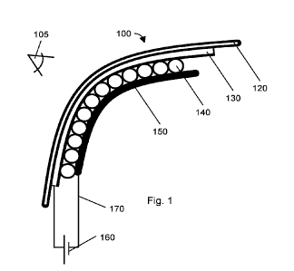
[Para 111 Fig. 1 shows a cross-sectional view of an embodiment of an
electrophoretic display
of the invention including a light-transmissive non-planar substrate including
a light-
transmissive conductor that is coupled to a voltage source. The voltage source
is also coupled
to a back conductor. A layer of encapsulated electrophoretic media is disposed
between the
light-transmissive conductor and the back conductor. One or more adhesive
layers may also
be present.
[Para 121 Fig. 2 illustrates that a variety of common objects can be made to
be color-changing
by molding a light-transmissive substrate and adding a front conductor, a
layer of
electrophoretic media, and a back conductor.
[Para 131 Fig. 3A illustrates a process for making a color-changing non-planar
display of the
invention.
[Para 141 Fig. 3B illustrates a process for making a color-changing non-planar
display of the
invention.
[Para 151 Fig. 4 illustrates an embodiment of a nozzle suitable for spray-
coating encapsulated
electrophoretic media.
[Para 161 Fig. 5 shows the preferred range of operation of a spray-coating
embodiment of the
invention.
DETAILED DESCRIPTION
[Para 171 The invention includes, inter al/a, a method for making a non-planar
electrophoretic
display including a light-transmissive front substrate that functions as a
viewing surface. A
light-transmissive conductive layer is incorporated into, or adhered to, the
light-transmissive
front substrate, whereupon a layer of electrophoretic encapsulated media is
attached thereto.
After the electrophoretic medium is deposited, a back electrode is attached or
deposited. When
a voltage is provided between the light-transmissive conductive layer and the
back electrode,
the image state of the electrophoretic medium is switched, thereby creating a
color-changing
surface. Such a color-changing surface can be incorporated into, e.g., a toy,
an appliance, an
electronic device, or other suitable structure.
Page 4
CA 03157989 2022-04-12
WO 2021/091936 PCT/US2020/058778
[Para 181 Some electro-optic materials are solid in the sense that the
materials have solid
external surfaces, although the materials may, and often do, have internal
liquid- or gas-filled
spaces. Such displays using solid electro-optic materials may hereinafter for
convenience be
referred to as "solid electro-optic displays". Thus, the term "solid electro-
optic displays"
includes rotating bichromal member displays, encapsulated electrophoretic
displays, microcell
electrophoretic displays and encapsulated liquid crystal displays.
[Para 191 The terms "bistable" and "bistability" are used herein in their
conventional meaning
in the art to refer to displays comprising display elements having first and
second display states
differing in at least one optical property, and such that after any given
element has been driven,
by means of an addressing pulse of finite duration, to assume either its first
or second display
state, after the addressing pulse has terminated, that state will persist for
at least several times,
for example at least four times, the minimum duration of the addressing pulse
required to
change the state of the display element. It is shown in U.S. Patent No.
7,170,670 that some
particle-based electrophoretic displays capable of gray scale are stable not
only in their extreme
black and white states but also in their intermediate gray states, and the
same is true of some
other types of electro-optic displays. This type of display is properly called
"multi-stable" rather
than bistable, although for convenience the term "bistable" may be used herein
to cover both
bistable and multi-stable displays.
[Para 201 One type of electro-optic display, which has been the subject of
intense research
and development for a number of years, is the particle-based electrophoretic
display, in which
a plurality of charged particles move through a fluid under the influence of
an electric field.
Electrophoretic displays can have attributes of good brightness and contrast,
wide viewing
angles, state bistability, and low power consumption when compared with liquid
crystal
displays. Nevertheless, problems with the long-term image quality of these
displays have
prevented their widespread usage. For example, particles that make up
electrophoretic displays
tend to settle, resulting in inadequate service-life for these displays.
[Para 211 Numerous patents and applications assigned to or in the names of the
Massachusetts
Institute of Technology (MIT) and E Ink Corporation describe various
technologies used in
encapsulated electrophoretic and other electro-optic media. Such encapsulated
media comprise
numerous small capsules, each of which itself comprises an internal phase
containing
electrophoretically-mobile particles in a fluid medium, and a capsule wall
surrounding the
internal phase. Typically, the capsules are themselves held within a polymeric
binder to form
Page 5
CA 03157989 2022-04-12
WO 2021/091936 PCT/US2020/058778
a coherent layer positioned between two electrodes. The technologies described
in these patents
and applications include:
(a) Electrophoretic particles, fluids and fluid additives; see for
example U.S. Patents Nos. 7,002,728; and 7,679,814;
(b) Capsules, binders and encapsulation processes; see for example
U.S. Patents Nos. 6,922,276; and 7,411,719;
(c) Films and sub-assemblies containing electro-optic materials; see
for example U.S. Patents Nos. 6,825,829; 6,982,178; 7,236,292; 7,443,571;
7,513,813; 7,561,324; 7,636,191; 7,649,666; 7,728,811; 7,729,039; 7,791,782;
7,839,564; 7,843,621; 7,843,624; 8,034,209; 8,068,272; 8,077,381; 8,177,942;
8,390,301; 8,482,852; 8,786,929; 8,830,553; 8,854,721; and 9,075,280; and
U.S. Patent Applications Publication Nos. 2009/0109519; 2009/0168067;
2011/0164301; 2014/0027044; 2014/0115884; and 2014/0340738;
(d) Backplanes, adhesive layers and other auxiliary layers and
methods used in displays; see for example U.S. Patents Nos. D485,294;
6,124,851; 6,130,773; 6,177,921; 6,232,950; 6,252,564; 6,312,304; 6,312,971;
6,376,828; 6,392,786; 6,413,790; 6,422,687; 6,445,374; 6,480,182; 6,498,114;
6,506,438; 6,518,949; 6,521,489; 6,535,197; 6,545,291; 6,639,578; 6,657,772;
6,664,944; 6,680,725; 6,683,333; 6,724,519; 6,750,473; 6,816,147; 6,819,471;
6,825,068; 6,831,769; 6,842,167; 6,842,279; 6,842,657; 6,865,010; 6,967,640;
6,980,196; 7,012,735; 7,030,412; 7,075,703; 7,106,296; 7,110,163; 7,116,318;
7,148,128; 7,167,155; 7,173,752; 7,176,880; 7,190,008; 7,206,119; 7,223,672;
7,230,751; 7,256,766; 7,259,744; 7,280,094; 7,327,511; 7,349,148; 7,352,353;
7,365,394; 7,365,733; 7,382,363; 7,388,572; 7,442,587; 7,492,497; 7,535,624;
7,551,346; 7,554,712; 7,583,427; 7,598,173; 7,605,799; 7,636,191; 7,649,674;
7,667,886; 7,672,040; 7,688,497; 7,733,335; 7,785,988; 7,843,626; 7,859,637;
7,893,435; 7,898,717; 7,957,053; 7,986,450; 8,009,344; 8,027,081; 8,049,947;
8,077,141; 8,089,453; 8,208,193; 8,373,211; 8,389,381; 8,498,042; 8,610,988;
8,728,266; 8,754,859; 8,830,560; 8,891,155; 8,989,886; 9,152,003; and
9,152,004; and U.S. Patent Applications Publication Nos. 2002/0060321;
2004/0105036; 2005/0122306; 2005/0122563; 2007/0052757; 2007/0097489;
2007/0109219; 2009/0122389; 2009/0315044; 2011/0026101; 2011/0140744;
2011/0187683; 2011/0187689; 2011/0292319; 2013/0278900; 2014/0078024;
Page 6
CA 03157989 2022-04-12
WO 2021/091936 PCT/US2020/058778
2014/0139501; 2014/0300837; 2015/0171112; 2015/0205178; 2015/0226986;
2015/0227018; 2015/0228666; and 2015/0261057; and International
Application Publication No. WO 00/38000; European Patents Nos. 1,099,207
B1 and 1,145,072 Bl;
(e) Color formation and color adjustment; see for example U.S.
Patents Nos. 7,075,502; and 7,839,564;
(f) Methods for driving displays; see for example U.S. Patents Nos.
7,012,600; and 7,453,445;
(g) Applications of displays; see for example U.S. Patents Nos.
7,312,784; and 8,009,348; and
(h) Non-electrophoretic displays, as described in U.S. Patents Nos.
6,241,921; 6,950,220; 7,420,549; 8,319,759; and 8,994,705; and U.S. Patent
Application Publication No. 2012/0293858.
[Para 221 Many of the aforementioned patents and applications recognize that
the walls
surrounding the discrete microcapsules in an encapsulated electrophoretic
medium could be
replaced by a continuous phase, thus producing a so-called polymer-dispersed
electrophoretic
display, in which the electrophoretic medium comprises a plurality of discrete
droplets of an
electrophoretic fluid and a continuous phase of a polymeric material, and that
the discrete
droplets of electrophoretic fluid within such a polymer-dispersed
electrophoretic display may
be regarded as capsules or microcapsules even though no discrete capsule
membrane is
associated with each individual droplet; see for example, the aforementioned
U.S. Patent No.
6,866,760. Accordingly, for purposes of the present application, such polymer-
dispersed
electrophoretic media are regarded as sub-species of encapsulated
electrophoretic media.
[Para 231 Although electrophoretic media are often opaque (since, for example,
in many
electrophoretic media, the particles substantially block transmission of
visible light through the
display) and operate in a reflective mode, many electrophoretic displays can
be made to operate
in a so-called "shutter mode" in which one display state is substantially
opaque and one is light-
transmissive. See, for example, U.S. Patents Nos. 5,872,552; 6,130,774;
6,144,361; 6,172,798;
6,271,823; 6,225,971; and 6,184,856. Dielectrophoretic displays, which are
similar to
electrophoretic displays but rely upon variations in electric field strength,
can operate in a
similar mode; see U.S. Patent No. 4,418,346. Other types of electro-optic
displays may also be
capable of operating in shutter mode. Electro-optic media operating in shutter
mode may be
useful in multi-layer structures for full color displays; in such structures,
at least one layer
Page 7
CA 03157989 2022-04-12
WO 2021/091936 PCT/US2020/058778
adjacent the viewing surface of the display operates in shutter mode to expose
or conceal a
second layer more distant from the viewing surface.
[Para 241 The term "light-transmissive" is used in this patent and herein to
mean that the layer
thus designated transmits sufficient light to enable an observer, looking
through that layer, to
observe the change in display states of the electro-optic medium, which will
normally be
viewed through the electrically-conductive layer and adjacent substrate (if
present); in cases
where the electro-optic medium displays a change in reflectivity at non-
visible wavelengths,
the term "light-transmissive" should of course be interpreted to refer to
transmission of the
relevant non-visible wavelengths. The substrate will typically be a polymeric
film, and will
normally have a thickness in the range of about 1 to about 25 mil (25 to 634
m), preferably
about 2 to about 10 mil (51 to 254 m). The light-transmissive conductive
material may be, for
example, a thin metal or metal oxide layer of, for example, aluminum or ITO,
or may be a
conductive polymer. Poly(ethylene terephthalate) (PET) films coated with
aluminum or ITO
are available commercially, for example as "aluminized Mylar" ("Mylar" is a
Registered Trade
Mark) from E.I. du Pont de Nemours & Company, Wilmington DE, and such
commercial
materials may be used with good results in the front plane laminate. The light-
transmissive
conductive material may also include metal flakes, metal screen, conductive
polymers, carbon
nanotubes, graphene, or a combination thereof.
[Para 251 In an electrophoretic display, there are often one or more adhesive
layers in the
stack of layers. For example, there may be an adhesive layer between the
electrophoretic layer
and an electrode, and this layer of adhesive remains in the final display. Of
course, this adhesive
layer has significant effects on the electro-optic properties of the display.
Inevitably, some of
the voltage drop between the electrodes occurs within the adhesive layer, thus
reducing the
voltage available for driving the electrophoretic layer. The effect of the
adhesive tends to
become greater at lower temperatures, and this variation in the effect of
adhesive with
temperature complicates the driving of the display. The voltage drop within
the adhesive can
be reduced, and the low temperature operation of the display improved, by
increasing the
conductivity of the adhesive layer, for example by doping the layer with
tetrabutylammonium
hexafluorophosphate or other materials as described in U.S. Patents Nos.
7,012,735 and
7,173,752.
[Para 261 A cross section of an exemplary color-changing object 100 can be
seen in Fig. 1,
wherein the viewing surface is opposed to the viewer 105. The color-changing
object 100 is
built up from a light-transmissive non-planar substrate 120, and then a light-
transmissive front
Page 8
CA 03157989 2022-04-12
WO 2021/091936 PCT/US2020/058778
conductor 130 is added as a separate layer or integrated into the light-
transmissive non-planar
substrate 120. After the light-transmissive non-planar substrate 120 and light-
transmissive
front conductor 130 are integrated, a layer of encapsulated electrophoretic
media 140 is
disposed upon the integrated layers 120 and 130. Finally, a back conductor 150
is disposed on
the layer of encapsulated electrophoretic media 140, thereby completing the
color-changing
object 100. After completion, the light-transmissive front conductor 130 and
the back
conductor 150 are connected to a voltage source 160 with an electrical
connector 170 (e.g., a
wire or a trace). When a voltage is applied between the light-transmissive
front conductor 130
and the back conductor 150 electrophoretic particles in the encapsulated
electrophoretic
medium will move toward (or away from) the viewer 105, thereby producing the
effect of a
color change in the color-changing object 100. The voltage source 160 may be,
for example,
a D.C. voltage source, and it may be configured to provide one, two, three,
four, five, six,
seven, eight, or nine voltage levels. In some embodiments, the voltage source
160 will provide
a time varying voltage signal that may look like square waves in a voltage vs.
time profile. The
time varying voltage may be ramped, saw-toothed, or sinusoidal The voltage
source 160 may
supply a continuum of voltage levels and time dependencies, allowing unique
application of
voltage signals. In some embodiment, multiple voltage sources 160 may be
coupled between
the front conductor 130 and the back conductor 150.
[Para 271 The layer of encapsulated electrophoretic medium may comprise more
than one
type of charged pigment particles, e.g., as described in the patent above.
Accordingly, the
color-changing object 100 may alternate between, for example, white and black.
Alternatively,
the layer of encapsulated electrophoretic media 140 may comprise three
particles wherein the
first set of charged pigment particles is red, the second set of charged
pigment particles is green,
and the third set of charged pigment particles is blue. Alternatively, the
layer of encapsulated
electrophoretic media 140 may comprise three particles wherein the first set
of charged pigment
particles is red, the second set of charged pigment particles is black, and
the third set of charged
pigment particles is white. Alternatively, the layer of encapsulated
electrophoretic media 140
may comprise four particles wherein the first set of charged pigment particles
is white, the
second set of charged pigment particles is cyan, the third set of charged
pigment particles is
yellow, and the fourth set of charged pigment particles is magenta. Some sets
of the charged
pigment particles may be primarily light-scattering (e.g., reflective), while
other sets may be
subtractive (e.g., absorptive), while other sets may be light-transmissive.
Alternatively, the
layer of encapsulated electrophoretic media 140 may comprise four particles
wherein the first
Page 9
CA 03157989 2022-04-12
WO 2021/091936 PCT/US2020/058778
set of charged pigment particles is red, the second set of charged pigment
particles is green, the
third set of charged pigment particles is blue, and the fourth set of charged
pigment particles is
black. Alternatively, the layer of encapsulated electrophoretic media 140 may
comprise four
particles wherein the first set of charged pigment particles is red, the
second set of charged
pigment particles is yellow, the third set of charged pigment particles is
blue, and the fourth set
of charged pigment particles is black. Alternatively, the layer of
encapsulated electrophoretic
media 140 may comprise five sets of charged particles wherein the first set of
charged pigment
particles is red, the second set of charged pigment particles is yellow, the
third set of charged
pigment particles is blue, the fourth set of charged pigment particles is
black, and the fifth set
of charged pigment particles is white.
[Para 281 It is to be understood that the color-changing object 100 need not
be rigid, and can
be flexible to the degree that bending does not cause rupture of the capsules
within the layer of
encapsulate electrophoretic media or cause the connections in the light-
transmissive front
conductor 130 or the back conductor 150 to fail. For example, the light-
transmissive non-
planar substrate 120 may comprise a clear polymer, such as polyethylene
terephthalate (PET),
polycarbonate, polypropylene, acrylic, or cyclic olefin copolymer (COC). It is
appropriate for
the light-transmissive non-planar substrate 120 to be only partially light-
transmissive, e.g.,
translucent and/or tinted. Such a light-transmissive non-planar substrate 120
may give rise to
a color-changing toy 200, such as shown in Fig. 2. Because the electrophoretic
medium only
requires a small amount of power, and because the electrophoretic states are
bistable, it is
possible to achieve such color-change features with a small energy source
(e.g., a disposable
battery) that is hidden within the color-changing object 100.
[Para 291 A method of making a color-changing object 100 is described with
respect to the
flow chart in Fig. 3A. Beginning with step 310 a light-transmissive non-planar
substrate is
provided. As discussed above, the light-transmissive non-planar substrate may
comprise a
clear polymer; however, other light-transmissive materials, such as glass, are
also suitable.
The light-transmissive non-planar substrate may be shaped before the process
begins with a
process such as thermoforming, casting, injection molding, blow-molding,
grinding, etching,
or cutting. After the light-transmissive substrate is provided in step 310, a
front (light-
transmissive) conductor is coupled to or integrated into the light-
transmissive substrate at step
320. In some embodiments, the front (light-transmissive) conductor may include
an
additional light-transmissive substrate, such as a PET film. As shown in FIG.
3B, in the
instance that the front conductor material is integrated into the light-
transmissive non-planar
Page 10
CA 03157989 2022-04-12
WO 2021/091936 PCT/US2020/058778
substrate 315, it is possible for the combination of the light-transmissive
non-planar substrate
and the front conductor to be shaped together, e.g., with thermoforming, blow
molding, etc.
Typically, the front (light-transmissive) conductor material comprises metal
flakes, metal
screen, conductive polymers, carbon nanotubes, graphene or a combination
thereof. The
front (light-transmissive) conductor material may be formed from a conductive
polymer, for
example poly(3,4-ethylenedioxythiophene) ("PEDOT"), normally used in the form
of its
poly(styrenesulfonate) salt ("PEDOT:PSS") or a polyaniline, or may be formed
from network
of conductors, for example carbon nanotubes or nanowires. If the front (light-
transmissive)
conductor material is not integrated into the light-transmissive non-planar
substrate, it may be
separately added to the light-transmissive non-planar substrate using a
process such as spray
coating, sputtering, atomic layer deposition, vapor deposition, painting, or
dip coating.
[Para 301 Once the light-transmissive non-planar substrate and the front
conductor have
been integrated, the resulting structure is coated with a layer of an
encapsulated
electrophoretic medium in step 330. This step may be accomplished using a
process such as
spray coating, dip coating, electrodeposition, powder coating, silk screening,
or brush-
painting. The encapsulated electrophoretic medium may be delivered as a slurry
of capsules
and a polyurethane binder, or the encapsulated electrophoretic medium may be
delivered
"freeze dried", i.e., after lyophilization. In order to provide a voltage
across the
electrophoretic medium to actuate the optical states, a back conductor is next
formed on the
layer of encapsulated electrophoretic media in step 340. The back conductor
need not be
light-transmissive; however, it may be light-transmissive. The back conductor
may comprise,
for example, metal flakes, metal screen, metal foil, metal paint, conductive
polymers, carbon
nanotubes, graphene, graphite or a combination thereof. Finally, once the
front and back
conductors are present, they may be connected to a voltage source in step 350.
In some
instances, it is useful to mask off a portion of the front conductor with,
e.g., masking tape,
prior to coating the non-planar object with the encapsulated medium and the
back conductor.
Accordingly, once the mask is removed, clear access to the front conductor is
provided to
allow easy coupling of the front and back conductors to the voltage source.
Alternatively, a
masking layer may be formed from a simple polymeric film that adheres to the
backplane
either because of its own physical properties or with the aid of an adhesive
coating, but
should desirably not be more than about 75 p.m in thickness. Polymeric films
that have been
found useful as masking layers include Kapton tape (a polyimide tape available
from du Pont
de Nemours & Company, Wilmington, DE) and RP301 film (an acrylic film
available form
Page 11
CA 03157989 2022-04-12
WO 2021/091936 PCT/US2020/058778
Nitto America, Inc., Fremont CA). The solid electro-optic layer is typically
an encapsulated
electrophoretic layer but may also be a polymer-dispersed electrophoretic
layer or a rotating
bichromal member or electrochromic layer. The material used to form the front
electrode and
the adhesive can be any of the materials used in the prior art for this
purpose.
[Para 311 For both the front (light-transmissive) conductor and the back
conductor, an
electrically conductive layer is disposed above and below, respectively, of
the layer of
encapsulated electrophoretic media. As discussed for example in the
aforementioned U.S.
Patent No. 6,982,178, polymeric films coated with indium tin oxide (ITO) are
available
commercially and are suitable for providing the front and the rear conductors.
In some
embodiments, an adhesive layer (not shown in figures) can be applied, e.g.,
between the light-
transmissive non-planar substrate and the front (light-transmissive)
conductor, or between the
front (light-transmissive) conductor and the layer of encapsulated
electrophoretic media, or
between the layer of encapsulate electrophoretic media and the back conductor.
Such an
adhesive may be cured, e.g., with heat and/or pressure, or the adhesive may be
radiation-cured
with ultraviolet radiation.
[Para 321 The front electrode layer 312 may be formed from a conductive
polymer, for
example poly(3,4-ethylenedioxythiophene) ("PEDOT"), normally used in the form
of its
poly(styrenesulfonate) salt ("PEDOT:PSS") or a polyaniline, or may be formed
from network
of conductors, for example carbon nanotubes or nanowires. The present
inventors have
successfully coated both PEDOT and carbon nanotube front electrodes directly
on an
encapsulated electrophoretic layer.
[Para 331 Spray coating process
[Para 341 As already mentioned, this invention may be constructed by spraying
capsules of
an electrophoretic medium on to a substrate. This process comprises forming a
dispersion of
the capsules in a liquid; feeding the dispersion through a first orifice; and
feeding a continuous
stream of gas through a second, annular orifice surrounding the first orifice,
thereby forming a
spray of the capsules. This spray coating process has the advantage over slot
coating that spray
coating normally does not require the use of rheology modifiers in the liquid
being sprayed, so
that the final coating is free from such rheology modifiers and hence free
from the effects such
rheology modifiers may have upon the properties of slot coated electrophoretic
media.
Typically, in spray coating, only the additives actually needed in the final
product need be
added to the liquid being sprayed.
Page 12
CA 03157989 2022-04-12
WO 2021/091936 PCT/US2020/058778
[Para 351 Figure 4 is a schematic cross-section through a simple spray coating
nozzle
(generally designated 600) that may be used in the spray coating process of
the present
invention. The nozzle 600 comprises a substantially cylindrical body 602
having a central, axial
bore 604 through which is pumped electrophoretic capsules (not shown)
dispersed in a liquid
(also not shown). The central bore 604 is surrounded by an annular bore 606,
through which is
forced a continuous stream of air. The lower end of the central bore 604
terminates in an orifice
608, which the lower end of the annular bore 606 terminates in an annular
orifice 610, which
surrounds orifice 608. A cylindrical baffle 612 surrounds the annular orifice
610. The air flow
through the annular orifice 610 constrained by the baffle 612 causes the
dispersion of capsules
passing through orifice 608 to form a spray or jet 614.
[Para 361 The nozzle 600 is also provided with shaping air bores 616, which
may be six or
eight in number. As shown in Fig. 4, the peripheral portions of the nozzle
600, through which
the bores 616 pass, extend downwardly below the orifices 608 and 610 and the
baffle 612, and
the lower portions of the bores 616 are directly downwardly and inwardly.
Shaping air is forced
continuously through the bores 616 so that it impinges on the jet 614, thereby
causing the jet
to open out into a wide spray 618, which impinges on a substrate 620 disposed
below the nozzle
600.
[Para 371 The quality of capsules coatings is assessed in terms of their
reproducibility
granularity, mean coating weight, uniformity and defect density; defect
density is quantified by
the number of non-switching capsules per unit display area in a standard
display structure,
which for present purposes is defined as a backplane bearing, in order, a 25
p.m layer of
lamination adhesive, a 20 p.m capsule layer and a front substrate comprising
an ITO layer on
25 p.m polyethylene terephthalate film. Preferably, the ratio of atomization
air outlet cross-
section to capsule dispersion outlet cross section is not greater than about
8.5, and preferably
between about 5.0 and about 7Ø The capsule dispersion orifice diameter is
preferably in the
range of about 1.0-1.40 mm. The capsule dispersion may contain capsules in a
weight fraction
preferably between about 38.0 and about 40.5 weight per cent; this dispersion
may optionally
contain 1-butanol at a concentration of up to about 4.0 weight per cent and a
surfactant, such
as Triton X-100 at a concentration of up to about 0.04 weight per cent.
[Para 381 A wide range of capsule dispersion feed rates and atomization air
feed rates can be
used in the spray coating process of the present invention. Typically, the
capsule dispersion
feed rate, MF, is not less than about 30 g/min and not greater than about 70
g/min, the optimum
being determined mainly on the basis of an appropriate residence time in the
atomization zone,
Page 13
CA 03157989 2022-04-12
WO 2021/091936 PCT/US2020/058778
that is to say the region in which the capsule dispersion column emerging from
the first orifice
breaks into sheets of fluid, which subsequently break into ligaments and
finally droplets.
Desirably, the droplet size distribution is such that the mean capsule count
per droplet is less
than about 5.0, and the standard deviation is less than about 3.0, capsules
per droplet. The
atomization air feed rate is set on the basis of a critical air velocity, v*,
measured at the second
orifice, and is typically of the order of about 100 m/sec. In the preferred
process, a total air feed
rate, MA, (including atomization air and shaping air) of approximately 150 to
200 g/min is
employed in the absence of shaping air, and up to 300 g/min with shaping air.
[Para 391 Empirically, it has been found that the operating window for HVLP
atomization in
terms of MA/MF versus MF, has the form shown in Fig. 5, although the numerical
values
involved will vary with the particular nozzle design used. The unshaded region
of the graph of
Fig. 5 represents the desirable operating window. The shaded regions represent
defect regions
which result in undesirable spray patterns such as excessive fluid velocity
("jetting"), highly
irregular and transient spray structure, and coarse droplet distribution.
[Para 401 In the spray coating process of the present invention, the air feed
rate and nozzle-
to-substrate distance should be carefully controlled to avoid capsule damage.
In general, a
nozzle-to-substrate distance of 200 to 320 mm is optimal, and this distance
should be adjusted
approximately inversely to atomization air velocity squared.
[Para 411 It has also been found that the quality and uniformity of the
sprayed capsule coating
can be strongly influenced by pretreatment of the substrate and by additives
added to the
capsule dispersion. Useful pretreatments and additives include but are not
limited to:
1) Capsule dispersions that incorporate surfactants such as Triton X -100,
butanol
etc. to improve wetting of the substrate surface;
2) Pre-coating of the substrate surface with sub-layers incorporating
surfactants
such as Triton X-100, 1-butanol, and others possessing a detergent structure,
and
optionally a polyurethane latex;
3) Pre-treating the substrate with an atmospheric plasma or corona
discharge
treatment; and
4) The capsule dispersion may contain polymeric binders, for example a
polyurethane latex
[Para 421 As already mentioned, the spray coating process of the invention may
include the
use of a masking material covering part of the substrate so that, after
removal of the masking
material, capsules remain only on those portions of the substrate where the
masking material
Page 14
CA 03157989 2022-04-12
WO 2021/091936 PCT/US2020/058778
was not present. The masking material used to cover part of the substrate
should not be porous,
or at least should have low enough porosity to ensure that capsule deposition
on to the masked
areas of the substrate does not occur. The masking material should not
significantly absorb the
liquid (usually aqueous) in which the capsules are dispersed, and should be
placed close enough
to the surface of the substrate that lateral draft of capsules beneath the
masking material from
the unmasked regions of the substrate into the masked areas does not occur.
After the capsules
have been deposited on the substrate, the capsules may be dried (or otherwise
treated to form
a coherent layer, for example by exposure to radiation) with the masking
material still in
position, or the masking material may first be removed and then the capsules
dried or otherwise
treated. In either case, the physical properties of the masking material and
the capsule
dispersion should be chosen so that, during the removal of the masking
material, capsules are
not dragged into previously masked areas of the substrate, nor are capsules
removed from
unmasked areas (for example, by irregular tearing of a coherent dried layer of
capsules.
[Para 431 The masking film may comprise an adhesive pre-laminated on to the
surface on to
which the capsules are to be deposited, and a release film exposed to the
spray. After capsule
deposition, the release film is removed, followed by additional processing.
The resultant spray-
printed film may then be laminated to a backplane, which may be either
transparent or opaque.
[Para 441 It will be apparent to those skilled in the art that numerous
changes and
modifications can be made in the specific embodiments of the invention
described above
without departing from the scope of the invention. Accordingly, the whole of
the foregoing
description is to be interpreted in an illustrative and not in a limitative
sense.
Page 15