Note: Descriptions are shown in the official language in which they were submitted.
FLIP-CHIP BALL GRID ARRAY-TYPE INTEGRATED CIRCUIT
PACKAGE FOR VERY HIGH FREQUENCY OPERATION
[0001] The invention is in the field of integrated circuit packages. More
particularly, it concerns a
Flip-Chip Ball Grid Array (FCBGA)-type package, which is to say adapted to
carry a flip-chip (FC)
and to connect to a printed circuit board, through an array of solder balls
referred to as a Ball Grid
Array (BGA).
[0002] A Ball Grid Array (BGA) is a type of surface mount package used for
integrated circuits. A
BGA package can have more interconnection pins than a flat or dual inline
package (DIP), as the
entire bottom surface of the device can be used for interconnecting, instead
of just the perimeter.
The interconnections can also be shorter than in other types of packages, and
thus have lower
parasitic inductance, leading to better high frequency performance.
[0003] Flip-Chip (FC) technology is a process for interconnecting integrated
circuits (or "electronic
chips") to external circuits by means of solder bumps deposited on pads
located on the upper
surface of the chip. Solder bumps are deposited on the chip pads during the
final stage of chip
manufacturing. Then the chip is flipped over so that its top side is facing
down, and aligned so
that the bumps line up with corresponding pads on the external circuit; then
the bumps are re-
melted to complete the interconnection. This is in contrast to wire
connection, where the chip is
mounted upright and wires are used to interconnect the chip pads to external
circuitry. Compared
to the conventional bridging technique, this approach allows for further
miniaturization and a
reduction in parasitic inductances, leading to better high-frequency
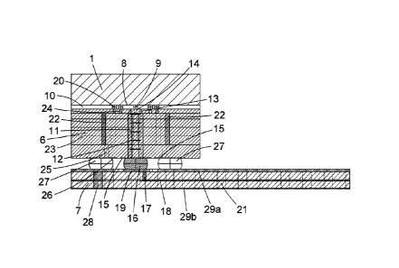
performance.
[0004] FCBGA packages combine the two technologies: on their underside they
carry an array
of solder balls to allow their interconnection to an external circuit
(typically a printed circuit board)
and, on their upper side they have conductive bumps to interconnect to a flip-
chip.
[0005] The flip-chip interconnection bumps have a spacing that is much smaller
than that of the
BGA arrays' solder balls. The FCBGA package must manage this step change
without causing
impedance breaks that would be detrimental to proper operation at very high
frequency (1 GHz
or more, even 10 GHz or more).
[0006] US 9,059,490 relates to an FCBGA package designed to operate at up to
60 GHz. The
underside of the package carries a "signal" ball surrounded by "ground" balls;
the signal ball is
connected to the central conductor of a microstrip transmission line carried
by a printed circuit
1
Date Recue/Date Received 2022-05-09
board, and the ground balls are connected to its ground conductors. A vertical
interconnection
("via") that passes through the dielectric body of the package and emerges
from its upper surface
is connected to each ball; the set of vias thus forms a quasi-coaxial
structure that is well-suited to
transmitting microwave signals. The central via connects the signal conductor
of a stripline
transmission line carried by a ceramic substrate, and the peripheral vias
connect this transmission
line's ground planes. Another smaller diameter quasi-coaxial structure of vias
that passes through
the ceramic substrate connects this line to a flip-chip fixed to the underside
of the ceramic
substrate, which protrudes laterally from the dielectric body of the package.
The use of a
transmission line interconnecting two quasi-coaxial structures of vias makes
it possible to adapt
the pitch of the BGA array and of the flip-chip, but at the expense of some
manufacturing
complexity and relatively significant dimensions.
[0007] US 6,891,266 and US 2006/0038633 relate to FCBGA packages comprising
quasi-
coaxial structures of vias that connect an array of solder balls on the
underside of the package to
a planar transmission line on its upper face. Again, the need to provide a
planar transmission line
on the package's upper face increases the package's dimensions.
[0008] The invention aims to overcome, in whole or in part, the aforementioned
drawbacks of the
prior art. More particularly, it aims to provide simpler and/or less bulky
FCBGA packages while
ensuring operation at frequencies that can exceed 10 GHz, or even 20 GHz, for
example up to
59 GHz.
[0009] According to the invention, this objective is achieved by using a quasi-
coaxial structure of
reduced-diameter vias in the upper part of the package to correspond to the
spacing between a
flip-chip's interconnection bumps. Furthermore, the signal is carried by a
plurality of vias at the
center of the structure, whose number decreases at the same time as the
diameter of the vias,
which makes it possible to maintain a constant impedance. In this way, the
change of spacing
happens within the set of vias, without needing to go through a transmission
line, which makes it
possible to reduce the complexity and the size of the package, while
maintaining good
performance at very high frequency.
[0010] According to a first aspect of the present disclosure there is provided
a flip-chip ball grid
array type integrated circuit package, comprising a dielectric body with an
upper face and an
underside in which:
2
Date Recue/Date Received 2022-05-09
- the underside of the dielectric body comprises a plurality of receiving
pads for connection
purposes, comprising a central signal receiving pad and peripheral ground
receiving pads
surrounding said signal receiving pad;
- a plurality of stacks of signal vias, electrically connected to the
signal receiving pad, and
passing vertically through said dielectric body;
- a plurality of stacks of ground vias, electrically connected to the
ground receiving pads,
passing vertically through said dielectric body and forming a ring around the
signal vias;
characterized in that, in an upper portion of the dielectric body:
- the signal vias are electrically connected to a lesser number of signal
conductive bumps
protruding from the upper face of the dielectric body; and
- at least two ground vias are connected, via conductive protrusions, to
respective ground
conductive bumps that protrude from the upper face of the dielectric body and
form a ring around
the signal conductive bumps.
[0011] The number of signal conductive bumps protruding from the upper face of
the dielectric
body may be less than the number of stacks of signal vias passing through the
dielectric body.
[0012] The conductive protrusions may extend from the at least two ground vias
and towards the
signal vias.
[0013] The lesser number of signal conductive bumps may comprise one or more
signal
conductive bumps.
[0014] According to particular embodiments of the invention:
[0015] Said dielectric body may consist of a stack of dielectric layers.
[0016] Conductive ground planes can be arranged between at least some of said
dielectric layers,
the ground planes having openings that have substantially the same diameter
and are aligned in
a vertical direction perpendicular to the ground planes; the stacks of signal
vias, electrically
connected to the signal receiving area, can pass vertically through said
dielectric layers
corresponding to a central region of the ground planes' openings; the stacks
of ground vias,
electrically connected to the ground receiving pads, can pass vertically
through said dielectric
3
Date Recue/Date Received 2022-05-09
layers outside the ground planes' openings; and the ground vias connected by
means of
conductive projections to respective conductive bumps can be located on either
side of a said
ground plane's opening. In this case, all the ground vias can be connected by
means of said
conductive projections to respective conductive bumps located inside said
opening.
[0017] The signal vias can be interconnected by conductive bridges
[0018] The stacks of ground vias may not extend through a lower portion of the
package, the
electrical connection with the ground receiving pads then being provided by
other stacks of vias,
forming a larger diameter ring around the signal vias than the ring formed by
the ground vias.
[0019] The dielectric body may be made of either ceramic material or organic
material.
[0020] The package may include a single signal-conducting bump.
[0021] The diameter of the ground planes' openings, the number of stacks of
signal vias, the
diameter of the ring(s) of vias around the signal vias, the number of ground
conductive bumps
and the diameter of the ring that these last shapes form around the signal
bump(s) can be chosen
to ensure continuity of impedance between the receiving pads for the solder
balls and the
conductive bumps protruding from the upper face of the dielectric body.
[0022] The package may carry a semiconductor flip-chip that is electrically
connected to the
conductive bumps protruding from the upper face of the dielectric body.
[0023] According to another aspect of the present disclosure there is provided
a printed circuit
board comprising a signal conductor and at least one ground plane forming a
transmission line
for microwave signals, the integrated circuit board carrying a package
according to the first aspect,
the signal receiving pad of said package being connected to said signal
conductor by means of a
solder ball and the ground receiving pads of said package being connected to
said ground
plane(s), also by means of solder balls.
[0024] Other characteristics, details and advantages of the invention will
become apparent upon
reading the description given in reference to the appended drawings provided
as an example and
that represent, respectively:
[0025] Fig.1 is a perspective view of a package according to the embodiment;
4
Date Recue/Date Received 2022-05-09
[0026] Fig. 2 is a first cross-sectional view of the package in Fig. 1
according to a first embodiment
of the invention, based on ceramic technology;
[0027] Fig. 3 is a second cross-sectional view of the package in Fig. 1
according to said first
embodiment of the invention;
[0028] Fig. 4 is a third cross-sectional view of the package in Fig. 1
according to said first
embodiment of the invention;
[0029] Fig. 5 is a transparent view of the package in Fig. 1 according to said
first embodiment of
the invention;
[0030] Fig. 6, is a first cross-sectional view of the package in Fig. 1
according to a second
embodiment of the invention, based on organic technology;
[0031] Fig. 7, is a second cross-sectional view of the package in Fig. 1
according to said second
embodiment of the invention;
[0032] Fig. 8, is a transparent view of the package in Fig. 1 according to
said second embodiment
of the invention; and
[0033] Fig. 9, is a detailed view of a stack of vias according to said second
embodiment of the
invention.
[0034] Fig. 1 shows an FCBGA package 2 mounted on a printed circuit board
(PCB) 5 by means
of a solder ball array 4 on its underside and bearing a flip-chip 1 on its
upper face.
[0035] Fig. 2, Fig. 3 and Fig. 4 show three cross-sectional views ¨ according
to sections A-A, B-
B and C-C respectively ¨ of package 2 according to a first embodiment made of
ceramic material.
Fig. 5 is a transparent view of this same package 2.
[0036] PCB 5 comprises a dielectric body 7, inside which is arranged a signal
line 18 arranged
between an upper ground plane 29a, on the upper surface of the PCB, and a
lower ground plane
29b, on the bottom surface of the PCB, and is framed by screening vias 21
connecting the two
ground planes. The signal line 18 is connected by means of a micro-via 17 to
an interconnection
area ("land") 19 located on the upper face of the PCB and insulated from the
ground planes; a
so-called "signal" solder ball 16 is arranged on this interconnection pad 19.
So-called "ground"
Date Recue/Date Received 2022-05-09
solder balls 27 are arranged on the upper ground plane 29a so as to surround
the signal ball 16.
Corresponding to the ground balls 27, ground vias 28 connect the upper ground
plane 29a to the
lower ground plane 29b.
[0037] The body of package 2 consists of a stack of dielectric layers (of
ceramic material, in the
embodiments of Fig. 2 - Fig. 4). Optionally, all or some of these dielectric
layers, and in particular
the upper dielectric layer of the stack, carry on their upper face a
conductive ground plane 23.
These conductive ground planes have vertically-aligned central openings 31.
The underside of
the package 2 carries conductive receiving pads corresponding to the solder
balls: a central signal
receiving pad 15 for the interconnection with the signal ball 19 and
peripheral ground receiving
pads 26 surrounding said signal receiving area 15 and intended for
interconnection with the
ground balls 27. The upper face of the package carries conductive bumps 9, 20
intended to allow
interconnection with the active face 8 of the flip-chip 1. More specifically,
one or more signal
conductive bumps 9 are surrounded by ground conductive bumps 20. Vias
extending through the
dielectric stack connect the signal conductive bump or bumps 9 to the signal
receiving pads 15
on the underside, and the ground conductive bumps 20 to the ground receiving
pads 26. The
space between the upper surface of the package 2, the conductive bumps and
chip 1 is filled with
an "underfill" resin 10.
[0038] The signal propagating along signal line 18 is vertically routed
directly to chip 1 by a
plurality of stacked signal vias 11, two in the illustrated embodiment,
interconnected by means of
conductive bridges 12. In the upper part of the stack (which is to say in the
upper dielectric layer)
these vias ¨ identified by reference 13 ¨ have a reduced radius for
feasibility reasons.
[0039] The use of bridges 12, which is non-essential, makes it possible to
increase the frequency
of a resonance that limits the interconnection's RF bandwidth, this resonance
being produced by
the signal rebounding between a possible impedance fault at the crossing of
the PCB - package
interface and at the crossing of the package - chip interface, marked by the
surface current density
rotating around a horizontal axis inside the plurality of signal vias 11 then
acting in the manner of
a resonant cavity. Indeed these bridges reduce the resonant cavity's volume
and thus the
resonant frequency's wavelength, and thus increase the package's maximum
frequency of use.
[0040] The stacks of signal vias 11 are surrounded by an ideally-concentric
ring composed of a
plurality of stacked ground vias 22, eight of them in the illustrated
embodiment. The number of
stacks of signal vias 11 and the diameter (more generally: the lateral
dimensions) of the ring of
6
Date Recue/Date Received 2022-05-09
stacked ground vias 22 are chosen such that the characteristic impedance of
the quasi-coaxial
structure 11, 22 is substantially identical to that of the transmission line
18, 29a, 29b, typically 50
Ohm. More specifically, for a given value of characteristic impedance, the
higher the number of
stacks of signal vias 11, the further apart the stacks of ground vias 22
should be.
[0041] If the dielectric layers of the package body carry ground planes 23
with central openings
31, the stacks of ground vias 22 are located outside of said openings, for
example in a position
tangential to their edges. The stacks of signal vias 11, on the other hand,
are found in the center
of said openings.
[0042] The spacing of the conductive ground bumps 20, which corresponds to
that of the pads
on the active face 8 of the chip 1 (not shown), is typically tighter than that
of the stacks of ground
vias 22. If this were not the case, the chip would have to have an
unnecessarily increased surface
area, which would increase the cost. As can be seen in Fig. 3, the stacks of
ground vias 22 stop
before reaching the top layer (or, more generally, a group of top layers) of
the dielectric stack.
This last layer is crossed through by ground vias 24 which also form a ring
around the signal vias
11, but of a smaller diameter to correspond to the positioning of respective
pads on the active
face 8 of the chip 1. More specifically, the vias 24 are inside the opening 31
of the ground plane
23 located between the upper dielectric layer and the one that is immediately
below it, and are
connected to this ground plane (or to the upper end of the stacks of vias 22)
by conductive
projections 30. The ground conductive bumps 20 are arranged corresponding to
the upper ends
of the vias 24.
[0043] The narrowing of the circular ring of ground vias tends to reduce the
characteristic
impedance of the quasi-coaxial structure. To avoid impedance breakdown, a
single signal
conducting bump 9 is laid on the top layer's bridge 12 (more typically, there
will be a lesser number
of signal bumps 9 than there are stacks of signal vias 11).
[0044] The decoupling of the radius of the ring of ground vias 24 on the upper
part of the body
of the package from the radius of the ring of ground vias 22 on the central
part of the body of the
package thus makes it possible to avoid an impedance fault appearing near the
chip's
interconnection. It should be noted that the electrical connection between the
ground vias 22 and
24 is made by a small width of copper (projections 30) to avoid creating a
capacitive fault
(decreased capacitive impedance) that would be produced by a narrowing of the
opening 31, and
therefore a rapprochement between the ground plane 23 and the signal vias 11.
7
Date Recue/Date Received 2022-05-09
[0045] In the lower part of the package body, the ring of ground vias 22 of
the central part gives
way to another ring of ground vias 25, of larger diameter. This makes it
possible, on the one hand,
to align, relatively, with the spacing of the ground balls 27, and, on the
other hand, to compensate
for the capacitive fault caused by the proximity between the ground balls'
receiving pads 26 and
the signal ball's receiving pad 15; this proximity, in turn, is due to the
significant size of these
receiving pads compared to the balls' footprint, which is typical of ceramic
substrate technology.
[0046] Fig. 6 and Fig. 7 show two cross-sectional views ¨ according to
sections A-A, and B-B
respectively ¨ of package 2 according to a second embodiment, made of organic
material. Fig. 8
is a transparent view of this same package.
[0047] As in the case of the ceramic package in Fig. 2¨ Fig. 5, the body of
package consists of
a stack of dielectric layers, this time made of organic material. More
specifically, it is possible to
distinguish a central part 34 consisting of thicker layers, or even one single
thick layer, and upper
and lower end parts 33 consisting of thinner layers. A solder-mask layer 32
can cover the upper
and lower faces, revealing only the electrical interconnection regions.
[0048] Compared to the embodiment made of ceramic material, the package made
of organic
material in Fig. 6 ¨ Fig. 8 can have receiving pads 15, 26 for smaller-
dimension solder balls. For
this reason, it is unnecessary to provide an enlargement of the ring of ground
vias in the lower
part of the package. In the upper part of the package, the signal can be
conveyed by a single
stack of vias 13.
[0049] The vias 22, 11 that pass through the package body made of organic
material can be
produced by laser ablation (as illustrated) or mechanically. The various
stacks of ground vias 25,
24 and of signal vias 13, 11 can be broken up so that the vias are not
strictly stacked but slightly
offset in relation to their counterpart in the top and/or bottom layer,
ideally offset by a capture pad
diameter, in order to improve the assembly's reliability and, more
specifically, the
thermomechanical stress resistance. Fig. 9 illustrates the structure of such a
stack of vias 200
(which may comprise a stack of ground vias 25, 24 and/or signal vias 13, 1 1
).
[0050] Certain features of the package in Fig. 6 ¨ Fig. 8 do not directly
result from the use of an
organic material, but constitute design choices. It basically involves that
the opening in the ground
planes is larger and square-shaped, and above all that only some of the ground
solder bumps are
brought closer to the signal solder bump, the other ground solder bumps
forming a ring of the
same lateral dimensions as the quasi-coaxial structure of vias 22. More
specifically, three ground
8
Date Recue/Date Received 2022-05-09
solder bumps on either side of the signal bump 9 are brought closer to the
signal bump 9 (it would
have been possible to bring together only two, but it is preferable to "split"
[or duplicate] one to
provide a passage for a signal line). The interconnection's sizing
(determining the number of
ground bumps to bring closer to the signal bump and their exact position) must
be done in such
a way as to ensure characteristic impedance continuity between the PCB and the
flip-chip.
[0051] The invention has been described in reference to two particular
embodiments, but variants
can be considered. Different dielectric and conductive materials can be
implemented, and
different fabrication techniques can be employed. The number, spacing and
relative position of
the signal and ground vias in the various parts of the package body (lower,
central, upper) can be
determined by the designer according to the specific constraints of each
application, while taking
care to ensure the absence of impedance faults throughout the interconnection.
Furthermore, the
package's dielectric body can be solid, although a multi-layer structure is
generally preferable. In
addition, the package may not be intended to be connected to a printed circuit
board via solder
balls, but to be placed in an adapter "socket", in which case the receiving
pads 15, 26 make
contact with spring connectors.
9
Date Recue/Date Received 2022-05-09