Note: Descriptions are shown in the official language in which they were submitted.
WO 2021/096770
PCT/US2020/059330
TRANSMITTER SIGNAL CANCELLATION IN PHASED ARRAY TRANSCEIVERS
This application claims the benefit under 35 U.S.C. 119(e) of Provisional
Application
Set. No. 62/934,148, filed November 12, 2019, entitled "Transmitter Signal
Cancellation in
Phased Array Receivers," the entire contents of which are incorporated herein
by reference.
TECHNICAL FIELD
The present invention generally relates to signal handling in phased array
transceivers
and more specifically to the attenuation of undesired signals on the receiver
sides of the phased
array transceivers.
BACKGROUND
In FDD (frequency division duplex) phased array systems, the transmitter
signal and
emissions are attenuated by way of a duplexer so that they do not desensitize
the receiver. There
are certain wireless bands where the duplex spacing is such that combinations
of transmit carriers
will result in intermodulation distortion products landing right on the
respective receive
channels. Although the duplexers have a large amount of transmit-to-receive
attenuation, they
do not always have enough for these cases and achieving higher attenuation is
often impractical.
In addition, these residual interrnodulation products tend to add up at the
output of the phased
array receive combiner because all transmitter signals are in-phase, which is
required for a
phased array system to operate.
SUMMARY
The embodiments described herein address the above-described problem by
introducing a
deliberate phase shift between the duplexer and the antenna element on every
other element in
the array, such that the phase of the transmitter signals and distortion
products are cancelled in
pairs at the receiver combiner. The phase shift can be implemented with a
simple delay element
(e.g., quarter wavelength transmission line) or with any other phase shifting
circuit arrangement.
In general, in one aspect the invention features a phased array system
including: an array
of antenna elements; and a plurality of transceivers, each including (1) a
transmitter chain; (2) a
receiver chain; and (3) a duplexer having a transmit input electrically
connected to the
1
CA 03158212 2022-5-12
WO 2021/096770
PCT/US2020/059330
transmitter chain, a receive output electrically connected to the receiver
chain, and a duplexed
port electrically connected to a corresponding different antenna element
within the array of
antenna elements. The plurality of transceivers includes a first subset of
transceivers and a
second subset of transceivers, wherein the first subset of transceivers
differs from the second
subset of transceivers in that each transceiver within the first subset of
transceivers further
comprises a 43 degree phase shifting element connected between the duplexed
port of the
duplexer within that transceiver and the antenna element to which the duplexed
port of that
duplexer is electrically connected, wherein 4) = -(2n+1)90 , and wherein n is
an integer.
Preferred embodiments include one or more of the following features. The
quantity ns:).
The number of transceivers in the first subset of transceivers and the number
of transceivers in
the second subset of transceivers is equal or approximately equal. The antenna
elements within
the array of antenna elements is organized into a plurality of columns and
wherein the antenna
elements in the odd numbered columns are connected to transceivers in the
first subset of
transceivers and the antenna elements in the even numbered columns are
connected to
transceivers in the second subset of transceivers. Alternatively, the antenna
elements within the
array of antenna elements is organized into a plurality of rows and wherein
the antenna elements
in the odd numbered rows are connected to transceivers in the first subset of
transceivers and the
antenna elements in the even numbered rows are connected to transceivers in
the second subset
of transceivers.
In general, in another aspect the invention features a method employing an
array of
antenna elements and a plurality of transceivers, each including (1) a
transmitter chain; (2) a
receiver chain; and (3) a duplexer having a transmit input electrically
connected to the
transmitter chain, a receive output electrically connected to the receiver
chain, and a duplexed
port electrically connected to a corresponding different antenna element
within the array of
antenna elements. The method includes: identifying among the plurality of
transceivers a first
subset of transceivers and a second subset of transceivers such that together
the first and second
subsets of transceivers constitute all of the transceivers among the plurality
of transceivers; for
each transceiver within the first subset of transceivers, but not for the
transceivers within the
second subset of transceivers, introducing a 4) degree phase shift between the
duplexed port of
2
CA 03158212 2022-5-12
WO 2021/096770
PCT/US2020/059330
the duplexer within that transceiver and the antenna element to which the
duplexed port of that
duplexer is electrically connected, wherein (IP = -(2n+1)90 , and wherein n is
an integer.
Preferred embodiments include one or more of the following features. The
quantity n:).
For each transceiver among the plurality of transceivers, the transmitter
chain for that transceiver
defines a transmit signal path for that transceiver, and the method further
involves: for each
transceiver within the first subset of transceivers, but not for the
transceivers within the second
subset of transceivers, introducing +90 phase shift in the transmit signal
path of that transceiver.
Within each transceiver among the plurality of transceivers the receiver chain
for that transceiver
defines a receive signal path for that transceiver, and the method further
includes: for each
transceiver within the first subset of transceivers, but not for the
transceivers within the second
subset of transceivers, introducing +90 phase shift in the receive signal path
of that transceiver.
BRIEF DESCRIPTION OF THE DRAWINGS
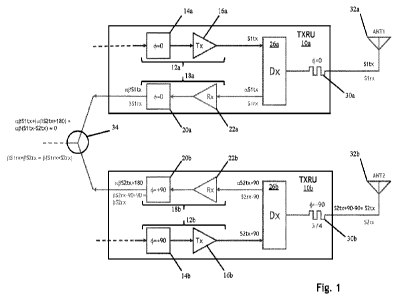
Fig. 1, using a simplified transceiver block diagram employing two array
elements,
illustraties the basic concept.
Fig. 2 illustrates an embodiment in which the delay element is outside of the
calibration
loop.
Fig. 3 illustrates an embodiment in which the delay element is inside of the
calibration
loop.
Fig. 4 illustrates an embodiment in which the delay element is inside of the
feedback
network.
Fig. 5 is an exemplary high-level block diagram showing the internal structure
of an
exemplary radio head and phased array antenna.
Fig. 6 is an exemplary high-level block diagram of a TuRx module such as is
shown in
Fig. 5.
Fig. 7 is an exemplary block diagram of the transmitter side of an active
antenna array
system showing the circuitry for only one of multiple transmit beams.
3
CA 03158212 2022-5-12
WO 2021/096770
PCT/US2020/059330
Fig. 8 is an exemplary block diagram of the receiver side of an active antenna
array
system showing the circuitry for only one of multiple receive beams.
The details of one or more embodiments of the invention are set forth in the
accompanying drawings and the description below. Other features, objects, and
advantages of
the invention will be apparent from the description and drawings, and from the
claims.
DETAILED DESCRIPTION
Referring to Fig. 1, a simplified transceiver block diagram is shown for two
array
elements. It shows two transceiver (TXRU) modules 10a and 10b, each of which
includes an RE
transmitter chain 12a, 12b (represented here by a phase rotator or phase
setting block 14a, 14b
and a Tx block 16a, 16b), an RE receiver chain 18a, 18b (represented here by a
phase rotator or
phase setting block 20a, 206 and an Rx block 22a, 22b), and a duple= 26a, 266
connecting the
transmitter and receiver chains to an antenna element 32a, 32b. The RE chains
perform the
digital-to-analog and analog-to-digital conversion and up-down conversion
operations, among
other things. The top transceiver 10a has no modifications and has no added
phase shifts. (For
reasons that will become apparent later, this is nevertheless represented by a
phase delay element
30a which in this example introduces a 0 degree phase shift between the
duplexer 26a and
antenna element 32a.) The bottom transceiver 10b includes a phase delay
element 306 that adds
a 900 phase delay on the duplexed line between the duplexer 26b and the
antenna element 32b.
The phase delay can be implemented by a quarter wavelength line that gives a
900 phase shift at
one frequency. Alternatively, a more complicated RE network that provides 900
phase shift
across a wide band of frequencies can be used.
This phase delay introduced by phase delay element 30b in TXRU 10b is seen by
both
the transmit and receive signals on the duplexed line. The phase delay is
compensated by phase
rotators 14b and 20b which are an integral part of any phased array system and
which in this case
guarantee that all of the transmit signals appear in-phase at each antenna
element and that the
receive signals appear in-phase at the inputs of a receiver combiner (or
aggregation network) 34.
In other words, the phase rotators 14b and 20b introduce a +90-degree phase
shift in the transmit
and receive signals. The difference between the first transceiver 10a and
second transceiver 10b,
however, is in the phase at which the residual transmitter signals from the
transceiver pair
4
CA 03158212 2022-5-12
WO 2021/096770
PCT/US2020/059330
appears at the output of the receiver phase combiner 34. The residual
transmitter signal from the
top transceiver 10a does not experience any phase shift in either the transmit
or receive path, so it
appears at the output of the receiver combiner 34 with no phase shift. The
residual transmitter
signal from the bottom transceiver 10b experiences two phase rotations, one in
the transmitter
chain 12b and one in the receiver chain 18b, and thus appears at the output of
the receiver
combiner 34 180' out of phase with that of the top transceiver 10a, resulting
in residual
transmitter signal cancellation.
With the phase delay elements as shown in Fig. 1, the signals at the various
locations in
the two transceiver modules are as follows. Assuming the transmit signal
delivered to the
duplexer 26a in the upper transceiver 10a is S ltx, the signal delivered to
the antenna element 32a
will be S ltx and the residual signal that leaks over onto the receive path
will be aS ltx, where a
is a measure of the coupling from the transmit side to the receive side of the
duplexer 26a.
Assuming the received signal is S lrx, the signal on the receiver line of the
duplexer 26a will be
S lrx and at the output of the receiver chain 18a will be PS in, where 1 is a
measure of the gain
that is applied by the receiver chain 18a as determined by the analog
beamforming precoding
weights that are applied. Similarly, the residual transmit signal that appears
at the output of the
receiver chain 18a will be apS ltx.
In the lower transceiver 10b, the transmit signal delivered to the duplexer
26b is
S2tx+90 and the signal delivered to the antenna element 32b will be S2tx +
900 - 90' or S2tx, as
desired. The residual signal that leaks over onto the receive path will be
aS2tx + 90 . Assuming
the received signal is S2rx, the signal on the receiver line of the duplexer
26b will be Sax - 90
and at the output of the receiver chain 18b will be PS2rx + 90 - 90 or
PS2tx, again as desired.
Similarly, the residual transmit signal that appears at the output of the
receiver chain will be
aPS2tx + 900 + 90 or oc13S2tx + 180', which is 180 out of phase with the
residual transmit
signal appearing at the output of the receiver chain 18a in the upper
transceiver 10a.
When the signals supplied by the two received signals are combined by the
aggregation
network, or the signal combiner network 34, the result is: 135 lrx +13S2rx.
And the combined
residual signals equal: af3S ltx + (cc13S2tx + 180 ). This equals afl(S ltx -
S2tx). If only the
phases are adjusted to achieve beamfonning, the magnitude of Si equals the
magnitude of 52
CA 03158212 2022-5-12
WO 2021/096770
PCT/US2020/059330
and the result is zero, La, the net residual signal is zero. If, on the other
hand, both the phases
and gains are adjusted to achieve beamforming (e.g. amplitude tapering is used
to reduce
sidelobes in the resulting beam), then S 1t--S2 and the result is
approximately zero which
nevertheless is a significant improvement over adding signal that are in
phase.
Note that in the case in which a quarter wavelength line is used to implement
the phase
delay element 30b between the duplexer 26b and the antenna element 32b, the
resulting phase
difference will differ by a small amount for frequencies that are offset from
the frequency for
which the quarter wavelength line is designed. Nevertheless, the resulting
cancellation at the
input of the combiner network 34 will still be large.
This paired element cancellation is implemented across the entire array, such
that the
resulting residual transmitter signal is minimized at the receive combiner
output. Without this
cancellation, the correlated residual transmitter signals would add linearly
with the number of
elements, resulting in 10logN addition of residual power at the output of the
receive combiner,
potentially causing receiver desensitization.
Note that all received signals (including the unwanted residual signals that
leak through
the duplexers 26a, 26b) appear at the receive combiner. So, if half of the
residual signals
experience the 90 phase delay and half of them do not (i.e., half will be at
0 phase and half will
be at 1800 phase), there will be total or near total cancellation. The
selection possibilities for
which antenna elements receive the phase delay and which do not are many. For
example, every
other antenna element in the array could be selected to apply to phase delay
or all of the antenna
elements in every other row (or column) of the array can be selected. If the
antenna array is
made up of an array of antenna sub-panels, the selection might be guided in
part by the way the
antenna sub-panels are designed and/or assembled together.
Also note that there are other combinations of phase delays that will also
mathematically
produce the same results, though they may not be as practical to implement. In
general, the
phase shift that is applied between the duple= and the antenna element can be
4)= -(2n+1)90 ,
wherein n is an integer. In that case, the phase shifts that would be applied
within the receiver
chain and the transmitter chain would be -4). The resulting residual transmit
signal that appears
6
CA 03158212 2022-5-12
WO 2021/096770
PCT/US2020/059330
at the output of the receiver chain would be ccI3S2tx + 2(2n+1)90 which can
be also written as
aP52tx + 4n90 + 2x90 = cx,PS2tx + n360 + 1800. So, again the resulting
residual signal at the
output of the receiver chain is 1800 out of phase with the residual signal
output by the other
receiver chain.
The underlying principles can be summarized as follows. The round-trip phase
offset for
the transmitter residual signals must be 180 degrees (or near 180 degrees) for
the phase shifted
elements (half of the elements). The transmitter phase shift must be net 0
degrees from the input
of the transmitter to its associated antenna element. And the receiver phase
shift must be net 0
degrees from its associated antenna element to the input of the receiver
combiner (or
equivalently, the output of the receiver chain).
Fig. 2 shows the paired element transceiver cancellation block diagram with
the addition
of a calibration loop which adjusts the phase of the transmit and receive
paths to ensure that
signals to and from all elements in the array are fully correlated and
coherent. The calibration
loop on the receive side includes an Rx feedback network 36 that senses the
signal on the output
line of the duplexer 26b via a sensor element 40 and provides a feedback
signal to the phase
setting element 20b. The calibration loop on the transmit side includes a Tx
feedback network
38 that senses the signal on the output line of the duplexer 26b via a sensor
element 42 and
provides a feedback signal to the phase setting element 14b. In this case, the
phase shift
introduced by phase delay element 30b is outside the calibration loops,
requiring a manual
adjustment of the transmit and receive path phase rotators for compensation.
More specifically,
the feedback for the calibration loop is taken from a location that is between
the duplexer 26b
and the phase delay element 30b. This is not the optimal solution, but it is
workable.
Note that the Rx and Tx feedback networks 36, 38 in the calibration loops are
implemented in known ways. For example, see the following patents which
disclose some
approaches: U.S. 10,225,067, entitled "Active Array Calibration," by Mihai
Banu and Yiping
Feng, issued March 5, 2019; and U.S. 10,009,165, entitled "Calibrating A
Serial
Interconnection", by Mihai Banu, issued June 26, 2018, both of which are
incorporated herein in
their entirety by reference.
7
CA 03158212 2022-5-12
WO 2021/096770
PCT/US2020/059330
Fig. 3 shows the paired element transceiver cancellation block diagram with
the phase
delay element 30b inside the calibration loop so that compensation is
automatically taken care of
as part of the phased array system calibration. More specifically, the
feedback for the calibration
loop is taken from a location that is between the phase delay element 30b and
the antenna
element 32b.
Fig. 4 shows the paired element transceiver cancellation block diagram which
excludes
the added phase delay element 30b, but with the addition of commensurate phase
shift elements
44, 46 added as part of the feedback loops. This alternative is shown for
cases where it may not
be advantageous or possible to have the feedback sense point after the added
phase shift element.
An example of an analog phased array system in which the above-described
approach can
be implemented is shown in Figs. 5-8.
Referring to Fig. 5, the antenna array 110 includes a two-dimensional array of
M antenna
elements. The radio head 190 includes multiple front-end modules (TXRU
modules) 200, equal
in number to the number of antenna elements in the array, namely, M. There is
a TXRU module
200 for each antenna element. There is also a signal distribution network 195
that includes an IF
distribution and aggregation network and an LO signal distribution network.
This signal
distribution network 195 delivers transmit signals from the BBU to the TXRU
modules 200,
delivers received signals from the TXRU modules 200 to the BBU, and provides
coherent local
oscillator signals to the TXRU modules 200 for up-converting IF transmit
signals to RE transmit
signals and for down-converting RF received signals to IF received signals.
Fig. 6 shows a block diagram of the circuitry that connects to a single
antenna element
210 of the multi-element antenna array. In the antenna array system having M
antenna elements,
this circuitry is duplicated for each antenna element. For each antenna
element 210, there is a
front-end module (or TXRU module) 200 connected to the antenna element 210.
The front-end
module has a transmitter side and a receiver side. The transmitter side
includes N up-conversion
modules 202 and a power amplifier (PA) 206. The receiver side includes a low
noise amplifier
(LNA) 212, and N down-conversion modules 216. The N up-conversion modules 202
enable the
array to generate N independent transmit beams and the N down-conversion
modules 216 enable
8
CA 03158212 2022-5-12
WO 2021/096770
PCT/US2020/059330
the array to generate N independent receive beams. (Note: In the case of the
illustrated example,
which is capable of generating only one beam, N=1.)
The front-end module 200 also includes a duplexer circuit 208 that couples the
drive
signal from the PA 206 on the transmitter side to the antenna element 210 and
couples a received
signal from the antenna element 210 to the LNA 212 on the receiver side. The
input of the up-
conversion module 202 is for receiving a beam transmit signal stream Bti from
the baseband unit
(not shown). And the output of the down-conversion module 216 is for
outputting a beam
received signal stream Br'.
An active antenna array system in which the up-conversion modules 202 are
shown in
greater detail is depicted in Fig. 7; and an active antenna array system in
which the down-
conversion modules 216 are shown in greater detail is depicted in Fig. 8. As a
practical matter,
these two systems, which are shown separately, would be implemented in the
same active
antenna array system but to simplify the figures, they are presented here
separately. The active
antenna array system of Fig. 7 is for transmitting one transmit signal stream
over a single
transmit beam that is generated by the M elements 210 of the antenna array.
Similarly, the active
antenna array system of Fig. 8 is for receiving a signal stream on a single
receive beam pattern
that is generated by the antenna array.
There is an LO distribution network 220 for distributing a coherent or phase
synchronized LO (local oscillator) signal to the M up-conversion modules 202
and the M down-
conversion modules 216. As shown in Fig. 7, there is also an IF distribution
network 224 for
delivering the IF transmit signal to each of the up-conversion modules 202.
And as shown in
Fig. 8, there is an IF aggregation network 226 for aggregating the received
signals from each of
the down-conversion modules 216.
The distribution and aggregation networks may be passive linear reciprocal
networks
with electrically identical paths to ensure the coherent
distribution/aggregation of signals.
Alternatively, one or more of these networks may be implemented using the
bidirectional
signaling network described in U.S. 8,259,884, entitled" Method and System for
Multi-Point
Signal Generation with Phase Synchronized Local Carriers," filed July 21, 2008
and U.S.
8,622,959, entitled "Low Cost, Active Antenna Arrays," filed June 30, 2011 or
the serial
9
CA 03158212 2022-5-12
WO 2021/096770
PCT/US2020/059330
interconnection approach described in U.S. 9,673,965, entitled "Calibrating a
Serial
Interconnection," filed September 8, 2016, the contents of all of which are
incorporated herein
by reference.
In general, each up-conversion module 202 includes a mixer 203 and various
amplitude
and phase setting circuits identified by A and P. respectively. The LO signal
and the distributed
IF transmit signal stream are both provided to the mixer 203 which up-converts
the IF transmit
signal stream to an RE transmit signal stream that is provided to the power
amplifier 206.
Similarly, each down-conversion module 216 also includes a mixer 217 and
various amplitude
and phase setting circuits similarly identified by A and P. respectively. The
mixer 217 in the
down-conversion module 216 multiplies the LO signal provided by the LO
distribution network
220 and the received RE signal stream from the low noise amplifier 212 that is
coupled to the
antenna element 210 to generate a down-converted IF received signal stream.
The down-
converted IF signal stream is provided to the IF aggregation network 226 for
aggregation with
the IF received signal streams from the other antenna elements and for
transfer back to the base
station.
The amplitude and phase setting circuits A and P are used for changing the
relative phase
or amplitude of individual antenna signals to thereby establish the size,
direction, and intensity of
the transmit and receive beam patterns that are generated by the antenna
array. (Note: In an
antenna array, a transmit beam is a radiation pattern that is generated by the
antenna array. That
radiation pattern can be measured in front of the antenna array. In contrast,
a receive beam is not
a radiation pattern formed by the antenna array but rather is a pattern of
antenna sensitivity.
Nevertheless, in spite of this difference, they are both generally referred to
as beams.) The
amplitude setting circuit is basically equivalent to a variable gain amplifier
in which the ratio of
the output signal amplitude to the input signal amplitude is programmable and
is set by
electronic control. The phase setting circuit has the fundamental capability
of shifting the input
signal in phase (or time) under electronic control. These amplitude and phase
setting circuits are
controlled by digital control signals (a.k.a. a beamforming precoding vector)
supplied by a
separate control processor 213.
CA 03158212 2022-5-12
WO 2021/096770
PCT/US2020/059330
The typology of the amplitude-setting and phase-setting circuits shown in
Figs. 7 and 8 is
just one of many possibilities for giving the basic transmitter and receiver
the capability to
control independently the amplitude and phase values of the individual antenna
signals. The
number and placement of the amplitude and phase setting circuits can vary from
what is
illustrated in Figs. 7 and 8. In addition, there are other components which
might be present in
the up-conversion and down-conversion modules but which are not shown in the
figures because
they are well known to persons skilled in the art. These might include, for
example, channel IF
filters and automatic gain controls.
Other embodiments are within the following claims. For example, the above
described
embodiments involve up-converting an IF signal to RU within the RU transmitter
chain in which
case the phase rotations are applied after up-conversion in the transmitter
chain (or before down-
conversion in the receiver chain). Alternatively, the up-converted RF signal
could be supplied
by the signal distribution network, in which case up and down conversion would
not take place
in the transceiver modules.
WHAT IS CLAIMED IS:
11
CA 03158212 2022-5-12