Note: Descriptions are shown in the official language in which they were submitted.
DIFFERENTIAL PAIR MODULE, CONNECTOR,
COMMUNICATIONS DEVICE, AND SHIELDING ASSEMBLY
poll This application claims priority to Chinese
Patent Application No. 201921986199.4,
filed with the China National Intellectual Property Administration on November
14, 2019 and
entitled "DIFFERENTIAL PAIR MODULE, CONNECTOR, COMMUNICATIONS DEVICE,
AND SHIELDING ASSEMBLY", which is incorporated herein by reference in its
entirety
TECHNICAL FIELD
[0002] This application relates to the field of
communications devices, and in particular, to a
differential pair module, a connector, a communications device, and a
shielding assembly
BACKGROUND
100031 A PCB board in a switch includes service line
cards and network switch cards. As
shown in FIG. 1, service line cards 11 and network switch cards 13 in a
conventional switch are
inserted into two opposite sides of a backplane 12 through connectors. A plane
in which the service
line cards 11 are located is perpendicular to a plane in which the network
switch cards 13 are
located. Signal interconnection is implemented between the service line cards
11 and the network
switch cards 13 by using the backplane 12. In such an architecture, the
backplane 12 divides
internal space of a chassis of the switch, resulting in relatively poor
ventilation and heat dissipation
performance of the chassis. In addition, a signal between the service line
cards 11 and the network
switch cards 13 needs to be transmitted by using a PCB trace of the backplane
12. Consequently,
a signal link is relatively long, and high-speed data transmission is
difficult to implement.
SUMMARY
[0004] This application provides a differential pair
module, a connector including the
differential pair module, and a communications device including the connector,
to directly connect
CA 03158424 2022-5-13 1
a service line card and a network switch card without using a backplane, so
that ventilation and
heat dissipation performance of the communications device can be improved, a
signal link can be
shortened, and the communications device can implement high-speed data
transmission.
[0005] According to a first aspect, this application
provides a differential pair module,
including a first signal terminal and a second signal terminal. The first
signal terminal includes a
first signal tail part, a first signal conductive connection part, and a first
signal body part connected
between the first signal tail part and the first signal conductive connection
part, the first signal
conductive connection part is connected in a bent manner to the first signal
body part, an extension
plane of the first signal conductive connection part and an extension plane of
the first signal body
part form an included angle, and an extension direction of the first signal
conductive connection
part and an extension direction of the first signal tail part form an included
angle. The second
signal terminal includes a second signal tail part, a second signal conductive
connection part, and
a second signal body part connected between the second signal tail part and
the second signal
conductive connection part, the second signal conductive connection part is
connected in a bent
manner to the second signal body part, an extension plane of the second signal
conductive
connection part and an extension plane of the second signal body part form an
included angle, and
an extension direction of the second signal conductive connection part and an
extension direction
of the second signal tail part form an included angle. The second signal body
part and the first
signal body part are laminated with a specific spacing and form a broadside
coupling, and the
second signal conductive connection part and the first signal conductive
connection part are
laminated with a specific spacing and form an edge coupling.
[0006] In this application, the differential pair
module is disposed on a first PCB board, and
includes two submodules assembled together, and each submodule includes a
signal terminal
(which is a generic term of the first signal terminal and the second signal
terminal, and this rule
also applies to the following description). The signal terminal is configured
to be inserted into a
connector on the second PCB board (which may be referred to as a second PCB
board connector).
A normal line of the extension plane of the signal body part and a normal line
of the extension
plane of the signal conductive connection part are along respective thickness
directions. That the
extension plane of the signal body part and the extension plane of the signal
conductive connection
part form an included angle means that the signal conductive connection part
is bent relative to the
signal body part. The included angle may be an acute angle, a right angle, or
an obtuse angle. The
CA 03158424 2022-5-13 2
extension direction of the signal conductive connection part is a direction in
which the signal
conductive connection part is inserted into the second PCB board connector.
The extension
direction of the signal tail part is a direction in which the signal tail part
is inserted into the first
PCB board. That the extension direction of the signal conductive connection
part and the extension
direction of the signal tail part form an included angle means that the signal
conductive connection
part is bent relative to the signal tail part. The included angle may be a
right angle or a non-right
angle.
100071 In this application, the broadside coupling
means that broader extension planes between
signal body parts are spaced relatively close to and face away from each
other, and a signal
coupling exists between the signal body parts. The edge coupling means that
narrower side
surfaces between signal conductive connection parts (the side surfaces are
vertically connected to
extension planes of the signal conductive connection parts) are spaced
relatively close to and
opposite to each other, and a signal coupling exists between the signal
conductive connection parts.
100081 In this application, the signal conductive
connection part is bent relative to the signal
tail part, and when the differential pair module is mounted at an edge of the
first PCB board, signal
tail parts are all inserted into the first PCB board, and the signal
conductive connection parts may
all protrude from a side edge of the first PCB board. This enables the
differential pair module to
adapt to an orthogonal placement manner of the first PCB board and the second
PCB board.
Because the signal conductive connection part is bent relative to the signal
body part, the signal
conductive connection part and the second PCB board connector can be directly
connected in
parallel to each other without using a relay of a backplane connector. In this
way, the differential
pair module can be used to implement a direct orthogonal interconnection
between the first PCB
board and the second PCB board, so that a communications device does not need
a backplane.
Because no backplane needs to be disposed, a signal link between the first PCB
board and the
second PCB board can be shortened, and the communications device can implement
high-speed
data transmission and has better ventilation and heat dissipation performance.
In addition, the
differential pair module can implement a transition from the broadside
coupling between signal
body parts to the edge coupling between signal conductive connection parts,
thereby satisfying a
product requirement.
[0009] In an implementation, the extension direction of the first signal
conductive connection
part is parallel to the extension plane of the first signal body part. Such a
structure is easy to process
CA 03158424 2022-5-13 3
and is convenient to implement insertion fitting with the second PCB board
connector.
[NW In an implementation, an angle value of the
included angle formed by the extension
plane of the first signal conductive connection part and the extension plane
of the first signal body
part is equal to an angle value of the included angle formed by the extension
plane of the second
signal conductive connection part and the extension plane of the second signal
body part. In this
way, the two signal terminals can form a corresponding structure, which is
convenient for
processing and for inserting into the second PCB board connector.
100111 In an implementation, the first signal tail part
is coplanar with the first signal body part,
and the second signal tail part is coplanar with the second signal body part.
Such a structure is easy
to process and is convenient to connect the signal tail part and the first PCB
board.
100121 In an implementation, the first signal body part
has a first region connected to the first
signal tail part, the second signal body part has a second region connected to
the second signal tail
part, the first region intersects with the second region, the first region is
bent towards the second
signal body part, and the second region is bent towards the first signal body
part, so that the first
signal tail part and the second signal tail part form an edge coupling. The
signal tail parts can form
the edge coupling through cross-twisting to satisfy requirements of signal
cable arrangement and
component arrangement on the first PCB board.
[0013] In an implementation, the differential pair
module includes a first ground terminal and
a second ground terminal; the first ground terminal is spaced from the first
signal terminal, the
first ground terminal includes a first ground body part and a first ground
part that are connected to
each other, the first ground body part is coplanar with the first signal body
part, and the first ground
part and the first signal tail part are located on a same side of the first
signal body part; and the
second ground terminal is spaced from the second signal terminal, the second
ground terminal
includes a second ground body part and a second ground part that are connected
to each other, the
second ground body part is coplanar with the second signal body part, and the
second ground part
and the second signal tail part are located on a same side of the second
signal body part.
[0014] In an implementation, the first ground part is
coplanar with the first ground body part,
and the second ground part is coplanar with the second ground body part. Such
a structure is easy
to process and can satisfy requirements of ground cable arrangement and
component arrangement
on the first PCB board.
[0015] In an implementation, one first signal terminal
is disposed between two first ground
CA 03158424 2022-5-13 4
terminals, and a first ground part of one of the two first ground terminals is
bent towards the second
ground body part and is coplanar with the second signal tail part to form an
edge coupling; one
second signal terminal is disposed between two second ground terminals, and a
second ground
part of one of the two second ground terminals is bent towards the first
ground body part and is
coplanar with the first signal tail part to form an edge coupling; and the
first ground part and the
second ground part forming the edge couplings are arranged diagonally. The
ground parts that
form the edge couplings may be connected to form one diagonal line of a
quadrangle, and ground
parts that do not form an edge coupling may be connected to form the other
diagonal line of the
quadrangle. Such a structure can satisfy requirements of ground cable
arrangement and component
arrangement on the first PCB board.
100161 In an implementation, both the first ground part
and the second ground part forming
the edge couplings form a fisheye structure. By using the fisheye structures,
the ground parts
forming the edge couplings are conveniently inserted into the first PCB board.
100171 In an implementation, the differential pair
module includes a first terminal bearing
member and a second terminal bearing member that are disposed in a laminated
manner; both the
first signal body part and the first ground body part are disposed on the
first terminal bearing
member, and the first signal conductive connection part, the first signal tail
part, and the first
ground part all extend outside the first terminal bearing member; and both the
second signal body
part and the second ground body part are disposed on the second terminal
bearing member, and
the second signal conductive connection part, the second signal tail part, and
the second ground
part all extend outside the second terminal bearing member. The terminal
bearing members can
reliably bear terminals (a generic term of signal terminals and ground
terminals) to ensure
transmission of electrical signals between the terminals. The terminal bearing
members may be
connected as a whole, or may be separately designed and then assembled
together.
[0018] In an implementation, the differential pair module includes a
first shielding bracket, a
first shielding member, a second shielding bracket, and a second shielding
member; the first
shielding bracket covers the first terminal bearing member, and the first
shielding member is
disposed on a side that is of the first shielding bracket and that faces the
first terminal bearing
member; and the second shielding bracket covers the second terminal bearing
member and is
located on a side that is of the second terminal bearing member and that faces
away from the first
terminal bearing member, and the second shielding member is disposed on a side
that is of the
CA 03158424 2022-5-13 5
second shielding bracket and that faces the second terminal bearing member.
Desirable
electromagnetic protection can be provided for the terminals and electrical
performance of the
terminals can be ensured by disposing the shielding brackets and the shielding
members. In
addition, the terminal bearing members that bear terminals can be packaged, to
provide a reliable
working environment for the terminals and enhance mechanical strength of the
entire differential
pair module.
[0019] In an implementation, a surface of the first
shielding bracket, a surface of the first
shielding member, a surface of the second shielding bracket, and a surface of
the second shielding
member are all provided with a conducting layer. An electromagnetic shielding
effect can be
improved by disposing the conducting layers.
100201 In an implementation, a surface that is of the
first terminal bearing member and that
faces the first shielding member and corresponds to the first signal body part
is provided with an
opening, and the first signal body part is exposed from the opening and is
spaced opposite to the
first shielding member. The opening may be located in the vicinity of the
first signal body part, for
example, in a thickness direction of the first signal body part. The opening
may fall within a
boundary of the first signal body part, or the opening may overlap the
boundary portion of the first
signal body part, or the first signal body part may fall within a boundary of
the opening. A shape,
a size, and a quantity of the opening may be set depending on a requirement.
For example, an
opening may be formed corresponding to a location of each first signal body
part. When there are
a plurality of openings, the openings are spaced from each other. Impedance
and signal attenuation
of the first signal terminal can be adjusted by disposing the opening.
[0021] In an implementation, a first limiting
protrusion is disposed on a surface that is of the
first shielding bracket and that faces the first terminal bearing member, the
first shielding member
has a first hollowed-out region, a first limiting through hole is disposed in
the first terminal bearing
member, and the first limiting protrusion passes through the first hollowed-
out region and is
inserted into the first limiting through hole. Fitting between the first
limiting protrusion and the
first limiting through hole can facilitate a connection between the first
shielding bracket and the
first terminal bearing member, and enhance insertion strength of the
differential pair module.
100221 In an implementation, a fitting through hole is
disposed in the first ground body part,
the fitting through hole corresponds to the first limiting through hole, and
the first limiting
protrusion is inserted into the first limiting through hole and the fitting
through hole. In this way,
CA 03158424 2022-5-13 6
the first limiting protrusion not only can connect the first shielding bracket
and the first terminal
bearing member, but also can separate adjacent first signal terminals, thereby
reducing signal
crosstalk between the adjacent first signal terminals.
[0023] In an implementation, there are a plurality of
first limiting protrusions, the plurality of
first limiting protrusions are spaced from each other, there are a plurality
of first limiting through
holes and a plurality of fitting through holes, and one limiting protrusion is
correspondingly
inserted into one limiting through hole and one fitting through hole. Fitting
between the plurality
of first limiting protrusions, the plurality of first limiting through holes,
and the plurality of fitting
through holes greatly enhances the insertion strength and reduces crosstalk.
[0024] In an implementation, a second limiting protrusion is disposed on
a surface that is of
the second shielding bracket and that faces the second terminal bearing
member, the second
shielding member has a second hollowed-out region, a second limiting through
hole is disposed in
the second terminal bearing member, the second limiting protrusion passes
through the second
hollowed-out region and is inserted into the second limiting through hole, and
the second limiting
protrusion is connected to the first limiting protrusion. Fitting between the
second limiting
protrusion and the second limiting through hole can facilitate a connection
between the second
shielding bracket and the second terminal bearing member, and enhance the
insertion strength of
the differential pair module. In addition, the two terminal bearing members
can be connected and
packaged through fitting between the second limiting protrusion and the first
limiting protrusion,
to form the differential pair module with reliable insertion strength.
[0025] According to a second aspect, this application
provides a connector, including several
differential pair modules. The connector can implement a PCB board
interconnection architecture
having no backplane, so that a communications device can implement high-speed
data
transmission and has better ventilation and heat dissipation performance. In
addition, the connector
can implement a transition from a broadside coupling between signal body parts
to an edge
coupling between signal conductive connection parts, thereby satisfying a
product requirement.
[0026] In an implementation, the connector includes an
assembling bracket, where the
assembling bracket is disposed on a same side of all the differential pair
modules, several first
through holes arranged at intervals are disposed on the assembling bracket,
one first signal tail part
and one second signal tail part thread through one first through hole
correspondingly, and neither
of them comes into contact with a hole wall of the first through hole. By
designing the assembling
CA 03158424 2022-5-13 7
bracket, all the differential pair modules can be connected to satisfy the
product requirement.
100271 In an implementation, several second through
holes arranged at intervals are disposed
on the assembling bracket; each differential pair module includes a first
ground terminal and a
second ground terminal, the first ground terminal is spaced from a first
signal terminal, the first
ground terminal includes a first ground body part and a first ground part that
are connected to each
other, the first ground body part is coplanar with a first signal body part,
and the first ground part
and a first signal tail part are located on a same side of the first signal
body part; the second ground
terminal is spaced from a second signal terminal, the second ground terminal
includes a second
ground body part and a second ground part that are connected to each other,
the second ground
body part is coplanar with a second signal body part, and the second ground
part and a second
signal tail part are located on a same side of the second signal body part;
and the first ground part
and the second ground part separately come into contact with a hole wall of
one second through
hole. The ground parts come into contact with inner walls of second through
holes of the
assembling bracket to implement grounding. The assembling bracket can serve as
a common
ground for all the differential pair modules.
[0028] According to a third aspect, this application
provides a communications device,
including a first PCB board, a second PCB board, a second PCB board connector,
and the
connector, where the first PCB board is perpendicular to the second PCB board,
and a side surface
of the first PCB board is opposite to a side surface of the second PCB board,
the second PCB board
connector is disposed on the second PCB board, a first signal tail part of the
connector is inserted
into the first PCB board, and a first signal conductive connection part is
inserted into the second
PCB board connector. The communications device uses a PCB board
interconnection architecture
having no backplane, so that the communications device can implement high-
speed data
transmission and has better ventilation and heat dissipation performance.
[0029] According to a fourth aspect, this application provides a
shielding assembly of a
connector. The shielding assembly includes a first shielding bracket and a
first shielding member,
the first shielding bracket and the first shielding member are laminated and
connected as a whole,
and both a surface of the first shielding bracket and a surface of the first
shielding member form a
conducting layer. The shielding assembly can implement electromagnetic
shielding of the
connector and enhance mechanical strength of the connector.
[0030] In an implementation, a first limiting
protrusion is formed on the surface of the first
CA 03158424 2022-5-13 8
shielding bracket, the first shielding member has a first hollowed-out region,
and the first limiting
protrusion passes through the first hollowed-out region. Such a structure is
relatively simple and
reliable, and can implement a connection between the first shielding bracket
and the first shielding
member.
WON In an implementation, there are a plurality of first limiting
protrusions, the plurality of
first limiting protrusions are spaced from each other, there are a plurality
of first hollowed-out
regions, and one first limiting protrusion correspondingly passes through one
first hollowed-out
region. Such a structure can enhance insertion strength between the first
shielding bracket and the
first shielding member.
[0032] In an implementation, the plurality of first limiting protrusions
are arranged in a
plurality of spaced rows, and a plurality of spaced first limiting protrusions
are included in each
row. Such a structure can enhance insertion strength between the first
shielding bracket and the
first shielding member.
100331 In an implementation, the shielding assembly
includes a second shielding bracket and
a second shielding member that are connected as a whole, the second shielding
member is adjacent
to the first shielding member, and the first shielding bracket and the second
shielding bracket are
disposed facing away from each other; and a second limiting protrusion is
formed on a surface of
the second shielding bracket, the second shielding member has a second
hollowed-out region, and
the second limiting protrusion passes through the second hollowed-out region
and is connected to
the first limiting protrusion. Such a structure can enhance insertion strength
of the shielding
assembly.
BRIEF DESCRIPTION OF DRAWINGS
100341 To describe technical solutions in embodiments
of this application or in the background,
the following describes the accompanying drawings required for describing the
embodiments of
this application or the background.
100351 FIG. 1 is a schematic diagram of a PCB board
interconnection architecture in a
conventional switch;
[0036] FIG. 2 is a schematic diagram of an overall
structure of a communications device
according to a first implementation of this application;
CA 03158424 2022-5-13 9
[0037] FIG. 3 is a schematic diagram of a PCB board
interconnection architecture in the
communications device in FIG. 2;
[0038] FIG. 4 is a schematic diagram of an assembly
structure of a connector in the
communications device in FIG. 2;
[00391 FIG. 5 is a schematic diagram of an overall structure of an
assembling bracket of the
connector in FIG. 4;
[0040] FIG. 6 is a schematic diagram of an assembly
structure of a differential pair module of
the connector in FIG. 4;
[0041] FIG. 7 is a schematic diagram of an exploded
structure of the differential pair module
in FIG. 6;
100421 FIG. 8 is a schematic diagram of an exploded
structure of a first submodule of the
differential pair module in FIG. 7;
[0043] FIG. 9 is a schematic diagram of a structure of
a first terminal bearing member that
bears first signal terminals and first ground terminals and that is in the
first submodule in FIG. 8;
[0044] FIG. 10 is a schematic diagram of an arrangement structure of the
first signal terminals
and the first ground terminals in FIG. 9;
100451 FIG. 11 is a schematic diagram of a structure of
the first signal terminal in FIG. 10;
[0046] FIG. 12 is a schematic diagram of a partially
enlarged structure of a location F in FIG.
11;
100471 FIG. 13 is a schematic diagram illustrating the structure of the
first ground terminal in
FIG. 10 and an arrangement relationship between the first ground terminal and
the first signal
terminal;
100481 FIG. 14 is a schematic diagram of a structure of
a first shielding bracket of the first
submodule in FIG. 8;
[0049] FIG. 15 is a schematic diagram of a cross-sectional structure of A-
A in FIG. 6;
NOW FIG. 16 is a schematic diagram of a partially
enlarged structure of a location B in FIG.
15;
[0051] FIG. 17 is a schematic diagram of an exploded
structure of a second submodule of the
differential pair module in FIG. 7;
[0052] FIG. 18 is a schematic diagram of a structure of a second terminal
bearing member that
bears second signal terminals and second ground terminals and that is in FIG.
17;
CA 03158424 2022-5-13 10
[0053] FIG. 19 is a schematic diagram of an arrangement
structure of the second signal
terminals and the second ground terminals in FIG. 18;
[0054] FIG. 20 is a schematic diagram of a structure of
the second signal terminal in FIG. 19;
[0055] FIG. 21 is a schematic diagram of a partially
enlarged structure of a location G in FIG.
20;
[0056] FIG. 22 is a schematic diagram illustrating the
structure of the second ground terminal
in FIG. 19 and an arrangement relationship between the second ground terminal
and the second
signal terminal;
[0057] FIG. 23 is a schematic diagram of a structure of
a second shielding bracket of the
second submodule in FIG. 17;
100581 FIG. 24 is a schematic diagram of a laminated
structure of terminals in a first
submodule and a second submodule;
[0059] FIG. 25 is a schematic diagram of a partially
enlarged structure of a location C in FIG.
24;
[0060] FIG. 26(a) is a schematic diagram of a side view structure in
which PCB boards are
connected by using a backplane in a conventional PCB board interconnection
architecture;
100611 FIG. 26(b) is a schematic diagram of a side view
structure of direct mutual fitting
between PCB boards in a PCB board interconnection architecture according to an
embodiment of
this application;
100621 FIG. 27 is a schematic diagram of a partially enlarged structure
of a location Dl in FIG.
24;
[0063] FIG. 28 is a schematic diagram of a partially
enlarged structure of a laminated structure
of terminals in a first submodule and a second submodule according to a second
implementation
of this application, where portions included in the partially enlarged diagram
D2 are consistent
with portions at the location D1 in FIG. 24;
100641 FIG. 29 is an L-direction view of a laminated
structure of terminals in a first submodule
and a second submodule according to a second implementation of this
application, where the L
direction is an L direction in FIG. 24;
100651 FIG. 30 is a schematic diagram of a partially
enlarged structure of a location E in FIG.
29;
[0066] FIG. 31 is a schematic diagram of a partial
laminated structure of terminals in a first
CA 03158424 2022-5-13 11
submodule and a second submodule according to a third implementation of this
application;
100671 FIG. 32 is an M-direction view of FIG. 31;
[0068] FIG. 33 is a schematic diagram of a structure of
an assembling bracket according to a
third implementation of this application; and
100691 FIG. 34 is a schematic diagram of a partially enlarged structure
of a location G in FIG.
33.
DESCRIPTION OF EMBODIMENTS
[MN As shown in FIG. 2, an embodiment of this
application provides a communications
device 20, including but not limited to a switch and a server. The
communications device 20
includes several PCB boards, and the PCB board may include a service PCB board
(which may
provide an external physical interface for service transmission to complete
packet receiving and
sending, and may also perform some protocol processing and switching/routing
functions) and a
switch PCB board (which may be responsible for data forwarding and switching,
packet switching,
distribution, scheduling, and control, and other functions). The PCB boards
are interconnected
through connectors.
[0071] Specifically, as shown in FIG. 3, the
communications device 20 may include a first
PCB board 22, a second PCB board 21, a first PCB board connector 23, and a
second PCB board
connector 24. The first PCB board 22 may be a switch PCB board (or a service
PCB board), the
second PCB board 21 may be a service PCB board (or a switch PCB board), and
there may be
several first PCB boards 22 and several second PCB boards 21. The first PCB
board 22 is
perpendicular to the second PCB board 21, and a side surface of the first PCB
board 22 is opposite
to a side surface of the second PCB board 21. The side surface is a surface
that has a relatively
small area in the PCB board and whose normal direction is perpendicular to a
thickness direction
of the PCB board. The first PCB board connector 23 is disposed at an edge of
the first PCB board
22, the second PCB board connector 24 is disposed at an edge of the second PCB
board 21, and
the first PCB board connector 23 is inserted into the second PCB board
connector 24, to
interconnect the first PCB board 22 and the second PCB board 21, thereby
implementing data
transmission.
100721 In this embodiment of this application, a
terminal of the first PCB board connector 23
CA 03158424 2022-5-13 12
has a bending design, and the second PCB board connector 24 is a conventional
connector.
Alternatively, a terminal of the second PCB board connector 24 may have a
bending design, and
the first PCB board connector 23 may be a conventional connector. The
following uses an example
for detailed description in which the first PCB board connector 23 (referred
to as a connector 23
for short below) has a bending design.
[0073] As shown in FIG. 4 to FIG. 6, in a first
implementation, the connector 23 may include
an assembling bracket 232 and several differential pair modules 231.
100741 As shown in FIG. 5, the assembling bracket 232
is in a shape of a flat plate and is
provided with several first through holes 232a and several second through
holes 232b. The first
through holes 232a and the second through holes 232b all penetrate through the
assembling bracket
232 along a thickness direction of the assembling bracket 232. The first
through hole 232a may be
greater than the second through hole 232b. The first through holes 232a and
the second through
holes 232b are spaced from each other to form a matrix. In a row (or column)
direction of the
matrix, the first through holes 232a and the second through holes 232b are
alternately arranged at
intervals. In a column (or row) direction of the matrix, several first through
holes 232a are
sequentially arranged at intervals to form a row, and several second through
holes 232b are
sequentially arranged at intervals to form a row.
[0075] The assembling bracket 232 is configured to
assemble all the differential pair modules
231 together, and serves as a common ground for all the differential pair
modules 231. Specifically,
the differential pair modules 231 are consecutively laminated, and the
assembling bracket 232 is
disposed on a same side surface of all the differential pair modules 231. One
first signal tail part
and one second signal tail part (described below) of each differential pair
module 231 thread
through one first through hole 232a correspondingly and are spaced from a hole
wall of the first
through hole 232a. One first ground part and one second ground part (described
below) of each
differential pair module 231 separately thread through one second through hole
232b
correspondingly and come into contact with a hole wall of the second through
hole 232b, so that
the differential pair module 231 is connected to the common ground.
[0076] As shown in FIG. 7, the differential pair module
231 may include a first submodule
233 and a second submodule 234, and the first submodule 233 and the second
submodule 234 are
laminated and assembled as a whole. The differential pair module 231 is
configured to transmit a
differential signal. The first submodule 233 is configured to transmit one
signal of the differential
CA 03158424 2022-5-13 13
signal, and the second submodule 234 is configured to transmit the other
signal of the differential
signal.
[0077] As shown in FIG. 7 to FIG. 10, the first
submodule 233 includes a first shielding bracket
2331, a first shielding member 2332, a first terminal bearing member 2333, a
first signal terminal
2335, and a first ground terminal 2334.
[0078] As shown in FIG. 9, the first terminal bearing
member 2333 is configured to bear and
protect first signal terminals 2335 and first ground terminals 2334. The first
terminal bearing
member 2333 may be a plate-shaped plastic part, and may be provided with a
plurality of rows of
first limiting through holes 2333a spaced from each other. A plurality of
first limiting through holes
2333a spaced from each other may be included in each row. Each first limiting
through hole 2333a
may penetrate through the first terminal bearing member 2333 along a thickness
direction of the
first terminal bearing member 2333. The first limiting through hole 2333a is
configured to be fitted
with the first shielding bracket (described below).
100791 The first terminal bearing member 2333, the
first signal terminals 2335, and the first
ground terminals 2334 may be connected as a whole by using an in-mold
injection molding process.
Through in-mold injection molding, plastics attached to the first signal
terminals 2335 and the first
ground terminals 2334 can form the first terminal bearing member 2333, and the
first limiting
through holes 2333a are formed in the first terminal bearing member 2333.
Certainly, the first
signal terminals 2335 and the first ground terminals 2334 may alternatively be
mounted on the
first terminal bearing member 2333 by using another process.
[0080] As shown in FIG. 9 and FIG. 10, on the first
terminal bearing member 2333, a plurality
of first signal terminals 2335 and a plurality of first ground terminals 2334
are alternately arranged
at intervals. To be specific, one first ground terminal 2334 is disposed
between two adjacent first
signal terminals 2335, and one first signal terminal 2335 is disposed between
two adjacent first
ground terminals 2334. In addition, one first signal terminal 2335 is located
between every two
adjacent rows of first limiting through holes 2333a.
[0081] In another implementation, a quantity and an
arrangement manner of the first limiting
through hole 2333a may be set depending on a requirement. For example, there
is at least one first
limiting through hole 2333a. The first limiting through hole 2333a may be
disposed at a required
location without being arranged in rows regularly Alternatively, the first
limiting through hole
2333 a may not be disposed.
CA 03158424 2022-5-13 14
[0082] As shown in FIG. 11, the first signal terminal
2335 may roughly be in a shape of a
narrow sheet. The first signal terminal 2335 may include a first signal
conductive connection part
23351, a first signal body part 23352, and a first signal tail part 23353. The
first signal body part
23352 is connected between the first signal conductive connection part 23351
and the first signal
tail part 23353. The first signal conductive connection part 23351 is
configured to be inserted into
the second PCB board connector 24, and the first signal tail part 23353 is
configured to be inserted
into the first PCB board 22.
100831 As shown in FIG. 11, the first signal body part
23352 may be in a shape of a narrow
sheet (a thickness Ti of the first signal body part 23352 is less than a width
WI of the first signal
body part 23352), and a thickness direction of the first signal body part
23352 may be consistent
with the thickness direction of the first terminal bearing member 2333. The
first signal body part
23352 has an extension plane Pl, and a normal line of the extension plane PI
is along the thickness
direction of the first signal body part 23352. A most portion of the first
signal body part 23352 is
embedded in the first terminal bearing member 2333, and a small portion of the
first signal body
part 23352 may protrude from the first terminal bearing member 2333 for a
relatively short
distance, so that the first signal conductive connection part 23351 is located
outside the first
terminal bearing member 2333. Certainly, the first signal body part 23352 may
alternatively be
disposed entirely inside the first terminal bearing member 2333, so that the
first signal conductive
connection part 23351 is located outside the first terminal bearing member
2333 and is adjacent to
the first terminal bearing member 2333.
[0084] As shown in FIG. 11, the first signal body part
23352 may have a bent shape, so that
an extension direction S2 of the first signal conductive connection part 23351
and an extension
direction Si of the first signal tail part 23353 form an included angle. The
included angle may be
a right angle or a non-right angle. The extension direction 52 of the first
signal conductive
connection part 23351 is a direction in which the first signal conductive
connection part 23351 is
inserted into the second PCB board connector 24, and the extension direction
Si is parallel to the
extension plane P 1 . The extension direction Si of the first signal tail part
23353 is a direction in
which the first signal tail part 23353 is inserted into the first PCB board
22, and the extension
direction S2 is parallel to the extension plane P1. Refer to FIG. 3. By using
the included-angle
formation design, the first signal terminal 2335 is conveniently connected
between the second PCB
board connector 24 and the first PCB board 22 whose side surfaces are opposite
to each other.
CA 03158424 2022-5-13 15
[0085] As shown in FIG. 11, the first signal conductive
connection part 23351 may be in a
shape of a narrow sheet (a thickness T2 of the first signal conductive
connection part 23351 is less
than a width W2 of the first signal conductive connection part 23351). The
first signal conductive
connection part 23351 has an extension plane P2, and a normal direction of the
extension plane P2
is a dimension direction of the thickness T2, that is, a thickness direction
of the first signal
conductive connection part 23351. The extension plane P2 and the extension
plane P1 are
connected and form a right angle. In this way, the first signal conductive
connection part 23351
and the first signal body part 23352 form a vertical bending structure. With
reference to FIG. 11
and FIG. 12, a bending line RI between the first signal conductive connection
part 23351 and the
first signal body part 23352 is along the extension direction S2 of the first
signal conductive
connection part 23351. The bending line RI passes through an arc transition
region between the
first signal conductive connection part 23351 and the first signal body part
23352 and serves as a
symmetry axis of the arc transition region.
100861 The vertical bending connection structure may be
implemented, for example, by using
a sheet metal processing technique. Punching or cutting is performed to obtain
the first signal
conductive connection part 23351 and the first signal body part 23352 that are
coplanar with each
other. The bending line RI is determined between the first signal conductive
connection part 23351
and the first signal body part 23352 based on the extension direction S2 of
the first signal
conductive connection part 23351, and then the first signal conductive
connection part 23351 is
vertically bent relative to the first signal body part 23352 along the bending
line RI by using a
bending process. The first signal conductive connection part 23351 may be bent
towards one side
of the first signal body part 23352, or may be bent towards an opposite side
(the one side and the
other side are two sides in the thickness direction of the first signal body
part 23352).
[0087] In another implementation, a bending angle
between the first signal conductive
connection part 23351 and the first signal body part 23352 may be an acute
angle or an obtuse
angle. In other words, the included angle formed by the extension plane P2 and
the extension plane
PI may be an acute angle or an obtuse angle, and/or the extension direction S2
of the first signal
conductive connection part 23351 may not be parallel to the extension plane P1
of the first signal
body part 23352.
[0088] As shown in FIG. 11, to ensure insertion strength and signal
transmission quality, the
first signal tail part 23353 may include a fisheye structure. Certainly, the
fisheye structure is not
CA 03158424 2022-5-13 16
mandatory. With reference to FIG. 5, the first signal tail part 23353 may
thread through a first
through hole 232a of the assembling bracket 232 and is spaced from a hole wall
of the first through
hole 232a.
[0089] As shown in FIG. 10 and FIG. 13, the first
ground terminal 2334 is spaced adjacent to
the first signal terminal 2335. The first ground terminal 2334 may include a
first ground body part
23342 and a first ground part 23341 that are connected to each other. With
reference to FIG. 13
and FIG. 9, the first ground body part 23342 is embedded in the first terminal
bearing member
2333, and the first ground body part 23342 is spaced adjacent to the first
signal body part 23352.
The first ground part 23341 is exposed outside the first terminal bearing
member 2333, and the
first ground part 23341 is spaced adjacent to the first signal tail part
23353. The first ground part
23341 and the first signal tail part 23353 are located on a same side of the
first terminal bearing
member 2333, that is, the first ground part 23341 and the first signal tail
part 23353 are located on
a same side of the first signal body part 23352. The first ground body part
23342 is configured to
be electrically connected to a ground terminal in the second PCB board
connector 24, and the first
ground part 23341 is configured to be grounded.
[0090] As shown in FIG. 13, the first ground body part
23342 may be in a shape of a narrow
sheet, and a thickness direction of the first ground body part 23342 is
basically consistent with the
thickness direction of the first terminal bearing member 2333. Several first
fitting through holes
hl spaced from each other may be disposed in the first ground body part 23342,
and the first fitting
through holes hl penetrate through the first ground body part 23342 along the
thickness direction
of the first ground body part 23342. The first fitting through holes hl in the
first ground body part
23342 are in a one-to-one correspondence with a row of first limiting through
holes 2333a in the
first terminal bearing member 2333. A single first fitting through hole hl at
least partially overlaps
a first limiting through hole 2333a corresponding to the first fitting through
hole hl. For example,
orthographic projections of the two through holes along axis directions of the
holes completely
overlap each other, or one projection falls within a boundary of the other
projection, or two
projections partially overlap each other. The first fitting through hole hi is
also configured to be
fitted with the first shielding bracket (described below).
[NM With reference to FIG. 5 and FIG. 13, the first
ground part 23341 may thread through
a second through hole 232b of the assembling bracket 232 and come into contact
with a hole wall
of the second through hole 232b to implement grounding. The first ground part
23341 may further
CA 03158424 2022-5-13 17
form a fisheye structure, to be conveniently inserted into the first PCB board
22 and connected to
a ground of the first PCB board 22. The fisheye structure can desirably ensure
insertion strength
and signal transmission quality Certainly, the first ground part 23341 may
alternatively not need
to include a fisheye structure. In another implementation, the structure and
connection manner of
the first ground terminal 2334 are not limited to those described above, and
the first ground
terminal 2334 may not even need to be disposed.
[0092] As shown in FIG. 8 and FIG. 14, the first
shielding bracket 2331 is approximately plate-
shaped, and covers and is connected to the first terminal bearing member 2333.
A thickness
direction of the first shielding bracket 2331 is basically consistent with
that of the first terminal
bearing member 2333. The first shielding bracket 2331 is further configured to
mount and bear the
first shielding member 2332. The first shielding bracket 2331 may be a plastic
part, and may be
molded by using an injection molding process.
[0093] As shown in FIG. 14, a surface of the first
shielding bracket 2331 may form a plurality
of rows of limiting protrusions 2331a that are spaced from each other, and a
plurality of limiting
protrusions 2331a arranged at intervals may be included in each row. A channel
is formed between
every two adjacent rows of limiting protrusions 2331a. With reference to FIG.
14 and FIG. 9, one
limiting protrusion 2331a is correspondingly inserted into one second fitting
through hole hl in
the first ground body part 23342 and one first limiting through hole 2333a in
the first terminal
bearing member 2333, and fits with the first fitting through hole hl and the
first limiting through
hole 2333a. The first shielding bracket 2331 and the first terminal bearing
member 2333 can be
assembled together by fitting the limiting protrusion 2331a with the first
fitting through hole hl
and the first limiting through hole 2333a. In addition, one first signal
terminal 2335 is
correspondingly accommodated in one channel, and two adjacent first signal
terminals 2335 are
separated by a row of limiting protrusions 2331a. This can reduce crosstalk
between adjacent first
signal terminals 2335.
100941 In another implementation, a specific quantity
and an arrangement manner of the
limiting protrusion 2331a may be set depending on a requirement, provided that
the limiting
protrusion 2331a can be fitted with at least some first fitting through holes
hl and at least some
first limiting through holes 2333a. For example, several limiting protrusions
233 la form a plurality
of rows, and there may be only one limiting protrusion 2331a in each row.
Alternatively, several
limiting protrusions 233 la may be arranged in a row, and a plurality of
limiting protrusions 233 la
CA 03158424 2022-5-13 18
spaced from each other are included in a single row of limiting protrusions
2331a. Alternatively,
the first shielding bracket 2331 may not be provided with a limiting
protrusion 2331a. The
foregoing structure of the first shielding bracket 2331 is not mandatory For
example, the first
shielding bracket 2331 may not be plate-shaped, may not be provided with a
limiting protrusion
233 ía, or even may be canceled.
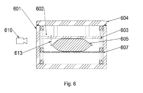
[0095] As shown in FIG. 8, the first shielding member
2332 may be a sheet-shaped metal piece,
and the first shielding member 2332 may be partially hollowed out to form a
first hollowed-out
region. The first shielding member 2332 is disposed on a side that is of the
first shielding bracket
2331 and that faces the first terminal bearing member 2333. The limiting
protrusion 233 ía passes
through the first hollowed-out region of the first shielding member 2332, and
a protrusion height
of the limiting protrusion 2331a may be greater than a thickness of the first
shielding member 2332.
The first shielding member 2332 may be nested at the root of the limiting
protrusion 2331a. The
first shielding member 2332 is located between the first shielding bracket
2331 and the first
terminal bearing member 2333. The first shielding member 2332 serves as a
reference ground
when the first signal terminal 2335 performs signal transmission, and has an
electromagnetic
shielding function. In this implementation, the first shielding member 2332
fills spacings between
the limiting protrusions 2331a. The spacings include a spacing between two
adjacent rows of
limiting protrusions 2331a and a spacing between two adjacent limiting
protrusions 2331a in a
single row of limiting protrusions 2331a. This can enhance isolation between
two adjacent first
signal terminals 2335, and further reduce crosstalk between the two adjacent
first signal terminals
2335.
[0096] The first shielding member 2332 and the first
shielding bracket 2331 may form an
integrated structure. A surface of the first shielding member 2332 may be
coated with plastics by
using an in-mold injection molding process, to form the integrated structure
including the first
shielding bracket 2331 and the first shielding member 2332. This integrated
structure has high
processing precision, and reduces a quantity of components that need to be
assembled in the first
submodule 233, thereby improving assembly precision and ensuring
electromagnetic shielding
stability. In addition, the first shielding member 2332 and the first
shielding bracket 2331 are
integrally formed through in-mold injection molding, without a need to first
obtain the first
shielding bracket 2331 through injection molding and then assemble the first
shielding bracket
2331 and the first shielding member 2332 together, so that costs can be
reduced.
CA 03158424 2022-5-13 19
[0097] To ensure an electromagnetic shielding effect,
electroplating processing may be
performed on the integrated structure formed by the first shielding member
2332 and the first
shielding bracket 2331, and both the surface of the first shielding member
2332 and the surface of
the first shielding bracket 2331 form a conducting layer. The conducting
layers may alternatively
be formed by using another process.
[0098] In another implementation, the first shielding
member 2332 and the first shielding
bracket 2331 may be separately designed, and then the first shielding member
2332 and the first
shielding bracket 2331 may be assembled. In this manner, several fitting
through holes may be
disposed on the first shielding member 2332, and the limiting protrusions
2331a on the first
shielding bracket 2331 pass through the fitting through holes. A quantity of
the fitting through hole
adapts to a quantity, a shape, and a location of the limiting protrusion
2331a. This fitting manner
can also increase a contact area between the first shielding member 2332 and
the first shielding
bracket 2331, thereby improving an electromagnetic shielding effect. Likewise,
to improve the
electromagnetic shielding effect, the conducting layers may be formed on the
surface of the first
shielding member 2332 and the surface of the first shielding bracket 2331.
Processes used for
forming the conducting layers are not limited to electroplating.
100991 As shown in FIG. 6, FIG. 15, FIG. 16, and FIG.
8, a surface that is of the first terminal
bearing member 2333 and that faces the first shielding member 2332 and
corresponds to the first
signal body part 23352 is provided with an opening 2333b. The "correspondence"
between the
opening 2333b and the first signal body part 23352 means that the opening
2333b is located in the
vicinity of the first signal body part 23352, for example, in the thickness
direction of the first signal
body part 23352. The opening 2333b may fall within a boundary of the first
signal body part 23352,
or the opening 2333b may overlap the boundary portion of the first signal body
part 23352, or the
first signal body part 23352 may fall within a boundary of the opening 2333b.
A shape, a size, and
a quantity of the opening 2333b may be set depending on a requirement. For
example, an opening
2333b may be formed corresponding to a location of each first signal body part
23352. When there
are a plurality of openings 2333b, the openings 2333b are spaced from each
other.
[00100] The opening 2333b may be obtained by hollowing out a material that is
of the first
terminal bearing member 2333 and that covers the first signal body part 23352,
and the first signal
body part 23352 is exposed from the opening 2333b and is spaced opposite to
the first shielding
member 2332.
CA 03158424 2022-5-13 20
[00101] Impedance and signal attenuation of the first signal terminal 2335 can
be adjusted by
disposing the opening 2333b. Depending on a product requirement, when the
impedance needs to
be increased, an opening 2333b with a larger size may be disposed to make an
opening area of the
opening 2333b larger; otherwise, an opening 2333b with a smaller size may be
disposed to make
an opening area of the opening 2333b smaller. To reduce signal attenuation, an
opening 2333b
with a larger size may be disposed to make an opening area of the opening
2333b larger. In another
implementation, the opening 2333b may not be disposed.
1001021 In this implementation, a structure of the second submodule 234 is
similar to that of the
first submodule 233, and is detailed below.
[00103] As shown in FIG. 16 to FIG. 18, the second submodule 234 includes a
second terminal
bearing member 2343, a second signal terminal 2345, a second ground terminal
2344, a second
shielding bracket 2341, and a second shielding member 2342.
[00104] As shown in FIG. 17 and FIG. 18, the second terminal bearing member
2343 is
configured to bear and protect second signal terminals 2345 and second ground
terminals 2344.
The second terminal bearing member 2343 may be a plate-shaped plastic part,
and may be
provided with a plurality of rows of second limiting through holes 2343a that
are spaced from each
other. A plurality of second limiting through holes 2343a spaced from each
other may be included
in each row. Each second limiting through hole 2343a may penetrate through the
second terminal
bearing member 2343 along a thickness direction. The second limiting through
hole 2343a is
configured to be fitted with the second shielding bracket (described below).
[00105] The second terminal bearing member 2343, the second signal terminals
2345, and the
second ground terminals 2344 may be connected as a whole by using an in-mold
injection molding
process. Through in-mold injection molding, plastics attached to the second
signal terminals 2345
and the second ground terminals 2344 can form the second terminal bearing
member 2343, and
the second limiting through holes 2343a are formed in the second terminal
bearing member 2343.
Certainly, the second signal terminals 2345 and the second ground terminals
2344 may
alternatively be mounted on the second terminal bearing member 2343 by using
another process.
[00106] As shown in FIG. 18 and FIG. 19, on the second terminal bearing member
2343, there
may be a plurality of second signal terminals 2345 and a plurality of second
ground terminals 2344,
and the plurality of second signal terminals 2345 and the plurality of second
ground terminals 2344
are alternately arranged at intervals. To be specific, one second ground
terminal 2344 is disposed
CA 03158424 2022-5-13 21
between two adjacent second signal terminals 2345, and one second signal
terminal 2345 is
disposed between two adjacent second ground terminals 2344.
[00107] In another implementation, a quantity and an arrangement manner of the
second
limiting through hole 2343a may be set depending on a requirement. For
example, there is at least
one second limiting through hole 2343a. The second limiting through hole 2343a
may be disposed
at a required location without being arranged in rows regularly.
Alternatively, the second limiting
through hole 2343a may not be disposed.
1001081 As shown in FIG. 20, the second signal terminal 2345 may roughly be in
a shape of a
narrow sheet. The second signal terminal 2345 may include a second signal
conductive connection
part 23451, a second signal body part 23452, and a second signal tail part
23453. The second signal
body part 23452 is connected between the second signal conductive connection
part 23451 and the
second signal tail part 23453. The second signal conductive connection part
23451 is configured
to be inserted into the second PCB board connector 24, and the second signal
tail part 23453 is
configured to be inserted into the first PCB board 22.
[00109] As shown in FIG. 20, the second signal body part 23452 may be in a
shape of a narrow
sheet (a thickness T3 of the second signal body part 23452 is less than a
width W3 of the second
signal body part 23452), and a thickness direction of the second signal body
part 23452 may be
basically consistent with the thickness direction of the second terminal
bearing member 2343. The
second signal body part 23452 has an extension plane P3 (a surface that is of
the second signal
body part 23452 and that faces downwards at a viewing angle in FIG. 20), and a
normal line of the
extension plane P3 is along the thickness direction of the second signal body
part 23452. A most
portion of the second signal body part 23452 is embedded in the second
terminal bearing member
2343, and a small portion of the second signal body part 23452 may protrude
from the second
terminal bearing member 2343 for a relatively short distance, so that the
second signal conductive
connection part 23451 is located outside the second terminal bearing member
2343. Certainly, the
second signal body part 23452 may alternatively be disposed entirely inside
the second terminal
bearing member 2343, so that the second signal conductive connection part
23451 is located
outside the second terminal bearing member 2343 and is adjacent to the second
terminal bearing
member 2343.
[00110] As shown in FIG. 20, the second signal body part 23452 may have a bent
shape, so that
an extension direction S4 of the second signal conductive connection part
23451 and an extension
CA 03158424 2022-5-13 22
direction S3 of the second signal tail part 23453 form an included angle. The
included angle may
be a right angle or a non-right angle. The extension direction S4 of the
second signal conductive
connection part 23451 is a direction in which the second signal conductive
connection part 23451
is inserted into the second PCB board connector 24, and the extension
direction S4 is parallel to
the extension plane P3. The extension direction S3 of the second signal tail
part 23453 is a direction
in which the second signal tail part 23453 is inserted into the first PCB
board 22, and the extension
direction S3 is parallel to the extension plane P3. Refer to FIG. 3. By using
the included-angle
formation design, the second signal terminal 2345 is conveniently connected
between the second
PCB board connector 24 and the first PCB board 22 whose side surfaces are
opposite to each other.
[00111] As shown in FIG. 20, the second signal conductive connection part
23451 may be in a
shape of a narrow sheet (a thickness T4 of the second signal conductive
connection part 23451 is
less than a width W4 of the second signal conductive connection part 23451).
The second signal
conductive connection part 23451 has an extension plane P4, and a normal
direction of the
extension plane P4 is a dimension direction of the thickness T4, that is, a
thickness direction of the
second signal conductive connection part 23451. The extension plane P4 and the
extension plane
P3 are connected and form a right angle. In this way, the second signal
conductive connection part
23451 and the second signal body part 23452 form a vertical bending structure.
With reference to
FIG. 20 and FIG. 21, a bending line R2 between the second signal conductive
connection part
23451 and the second signal body part 23452 is along the extension direction
S4 of the second
signal conductive connection part 23451. The bending line R2 passes through an
arc transition
region between the second signal conductive connection part 23451 and the
second signal body
part 23452 and serves as a symmetry axis of the arc transition region.
1001121 The vertical bending connection structure may be implemented, for
example, by using
a sheet metal processing technique. Punching or cutting is performed to obtain
the second signal
conductive connection part 23451 and the second signal body part 23452 that
are coplanar with
each other. The bending line R2 is determined between the second signal
conductive connection
part 23451 and the second signal body part 23452 based on the extension
direction S4 of the second
signal conductive connection part 23451, and then the second signal conductive
connection part
23451 is vertically bent relative to the second signal body part 23452 along
the bending line R2
by using a bending process. The second signal conductive connection part 23451
may be bent
towards one side of the second signal body part 23452, or may be bent towards
an opposite side
CA 03158424 2022-5-13 23
(the one side and the other side are two sides in the thickness direction of
the second signal body
part 23452).
[00113] With reference to FIG. 20 and FIG. 11,
considering that in the differential pair module
231, the second signal conductive connection part 23451 and the first signal
conductive connection
part 23351 are spaced opposite to each other and a spacing between them is
limited, the second
signal conductive connection part 23451 and the first signal conductive
connection part 23351
may be bent backwards, that is, both of them are bent in a direction facing
away from each other.
1001141 In another implementation, a bending angle between the second signal
conductive
connection part 23451 and the second signal body part 23452 may be an acute
angle or an obtuse
angle. In other words, the included angle formed by the extension plane P4 and
the extension plane
P3 may be an acute angle or an obtuse angle, and/or the extension direction S4
of the second signal
conductive connection part 23451 may not be parallel to the extension plane P3
of the second
signal body part 23452.
1001151 As shown in FIG. 20, to ensure insertion
strength and signal transmission quality, the
second signal tail part 23453 may include a fisheye structure. Certainly, the
fisheye structure is not
mandatory. With reference to FIG. 5, the second signal tail part 23453 may
thread through a first
through hole 232a of the assembling bracket 232 and is spaced from a hole wall
of the first through
hole 232a.
[00116] As shown in FIG. 19 and FIG. 22, the second ground terminal 2344 is
spaced adjacent
to the second signal terminal 2345. The second ground terminal 2344 may
include a second ground
body part 23442 and a second ground part 23441 that are connected to each
other. With reference
to FIG. 22 and FIG. 18, the second ground body part 23442 is embedded in the
second terminal
bearing member 2343, and the second ground body part 23442 is spaced adjacent
to the second
signal body part 23452. The second ground part 23441 is exposed outside the
second terminal
bearing member 2343, and is spaced adjacent to the second signal tail part
23453. The second
ground part 23441 and the second signal tail part 23453 are located on a same
side of the second
terminal bearing member 2343, that is, the second ground part 23441 and the
second signal tail
part 23453 are located on a same side of the second signal body part 23452.
The second ground
body part 23442 is configured to be electrically connected to a ground
terminal in the second PCB
board connector 24, and the second ground part 23441 is configured to be
grounded.
[00117] As shown in FIG. 22, the second ground body part 23442 may be in a
shape of a narrow
CA 03158424 2022-5-13 24
sheet, and a thickness direction of the second ground body part 23442 is
basically consistent with
the thickness direction of the second terminal bearing member 2343. Several
second fitting through
holes h2 spaced from each other may be disposed in the second ground body part
23442, and the
second fitting through holes h2 penetrate through the second ground body part
23442 along the
thickness direction of the second ground body part 23442. The second fitting
through holes h2 in
the second ground body part 23442 are in a one-to-one correspondence with a
row of second
limiting through holes 2343a in the second terminal bearing member 2343. A
single second fitting
through hole h2 at least partially overlaps a second limiting through hole
2343a corresponding to
the second fitting through hole 112. For example, orthographic projections of
the two through holes
along axis directions of the holes completely overlap each other, or one
projection falls within a
boundary of the other projection, or two projections partially overlap each
other. The second fitting
through hole h2 is also configured to be fitted with the second shielding
bracket (described below).
[00118] With reference to FIG. 5 and FIG. 22, the second ground part 23441 may
thread through
a second through hole 232b of the assembling bracket 232 and come into contact
with a hole wall
of the second through hole 232b to implement grounding. The second ground part
23441 may
further form a fisheye structure, to be conveniently inserted into the first
PCB board 22 and
connected to a ground of the first PCB board 22. The fisheye structure can
desirably ensure
insertion strength and signal transmission quality Certainly, the second
ground part 23441 may
alternatively not need to include a fisheye structure. In another
implementation, the structure and
connection manner of the second ground terminal 2344 are not limited to those
described above,
and the second ground terminal 2344 may not even need to be disposed.
[00119] As shown in FIG. 17 and FIG. 23, in this implementation, the second
shielding bracket
2341 is approximately plate-shaped, and covers and is connected to the second
terminal bearing
member 2343. A thickness direction of the second shielding bracket 2341 keeps
consistent with
that of the second terminal bearing member 2343. The second shielding bracket
2341 is further
configured to mount and bear the second shielding member 2342. The second
shielding bracket
2341 may be a plastic part, and may be molded by using an injection molding
process.
[00120] As shown in FIG. 23, a surface of the second shielding bracket 2341
may form a
plurality of rows of limiting protrusions 2341a that are spaced from each
other, and a plurality of
limiting protrusions 2341a spaced from each other may be included in each row.
A channel is
formed between every two adjacent rows of limiting protrusions 2341a. With
reference to FIG. 23
CA 03158424 2022-5-13 25
and FIG. 18, one limiting protrusion 2341a correspondingly passes through one
second fitting
through hole h2 in the second ground body part 23442 and one second limiting
through hole 2343a
in the second terminal bearing member 2343, and fits with the second fitting
through hole h2 and
the second limiting through hole 2343a. The second shielding bracket 2341 and
the second
terminal bearing member 2343 can be assembled together by fitting the limiting
protrusion 2341a
with the second fitting through hole h2 and the second limiting through hole
2343a. In addition,
one second signal terminal 2345 is correspondingly accommodated in one
channel, and two
adjacent second signal terminals 2345 are separated by a row of limiting
protrusions 2341a. This
can reduce crosstalk between adjacent second signal terminals 2345.
[00121] In another implementation, a specific quantity and an arrangement
manner of the
limiting protrusion 2341a may be set depending on a requirement, provided that
the limiting
protrusion 2341a can be fitted with at least some second fitting through holes
h2 and at least some
second limiting through holes 2343a. For example, several limiting protrusions
2341a form a
plurality of rows, and there may be only one limiting protrusion 2341a in each
row. The foregoing
structure of the second shielding bracket 2341 is not mandatory. For example,
the second shielding
bracket 2341 may not be plate-shaped, may not be provided with a limiting
protrusion 2341a, or
even may be canceled.
[00122] As shown in FIG. 17, the second shielding member 2342 may be a sheet-
shaped metal
piece, and the second shielding member 2342 may be partially hollowed out to
form a second
hollowed-out region. The second shielding member 2342 is disposed on a side
that is of the second
shielding bracket 2341 and that faces the second terminal bearing member 2343.
The limiting
protrusion 2341a passes through the second hollowed-out region of the second
shielding member
2342, and a protrusion height of the limiting protrusion 2341a may be greater
than a thickness of
the second shielding member 2342. The second shielding member 2342 may be
nested at the root
of the limiting protrusion 2341a. The second shielding member 2342 is located
between the second
shielding bracket 2341 and the second terminal bearing member 2343. The second
shielding
member 2342 serves as a reference ground when the second signal terminal 2345
performs signal
transmission, and has an electromagnetic shielding function. In this
implementation, the second
shielding member 2342 fills spacings between the limiting protrusions 2341a.
The spacings
include a spacing between two adjacent rows of limiting protrusions 2341a and
a spacing between
two adjacent limiting protrusions 2341a in a single row of limiting
protrusions 2341a. This can
CA 03158424 2022-5-13 26
enhance isolation between two adjacent second signal terminals 2345, and
further reduce crosstalk
between the two adjacent second signal terminals 2345.
[00123] The second shielding member 2342 and the second shielding bracket 2341
may form
an integrated structure. A surface of the second shielding member 2342 may be
coated with plastics
by using an in-mold injection molding process, to form the integrated
structure including the
second shielding bracket 2341 and the second shielding member 2342. This
integrated structure
has high processing precision, and reduces a quantity of components that need
to be assembled in
the second submodule 234, thereby improving assembly precision and ensuring
electromagnetic
shielding stability In addition, the second shielding member 2342 and the
second shielding bracket
2341 are integrally formed through in-mold injection molding, without a need
to first obtain the
second shielding bracket 2341 through injection molding and then assemble the
second shielding
bracket 2341 and the second shielding member 2342 together, so that costs can
be reduced.
[00124] To ensure an electromagnetic shielding effect,
electroplating processing may be
performed on the integrated structure formed by the second shielding member
2342 and the second
shielding bracket 2341, and both the surface of the second shielding member
2342 and the surface
of the second shielding bracket 2341 form a conducting layer. The conducting
layers may
alternatively be formed by using another process.
[00125] In another implementation, the second shielding member 2342 and the
second shielding
bracket 2341 may be separately designed, and then the second shielding member
2342 and the
second shielding bracket 2341 may be assembled. In this solution, several
fitting through holes
may be disposed on the second shielding member 2342, and the limiting
protrusions 2341a on the
second shielding bracket 2341 pass through the fitting through holes. A
quantity of the fitting
through hole adapts to a quantity, a shape, and a location of the limiting
protrusion 2341a. This
fitting manner can also increase a contact area between the second shielding
member 2342 and the
second shielding bracket 2341, thereby improving a ground shielding effect.
Likewise, to improve
an electromagnetic shielding effect, the conducting layers may be formed on
the surface of the
second shielding member 2342 and the surface of the second shielding bracket
2341. Processes
used for forming the conducting layers are not limited to electroplating.
1001261 As shown in FIG. 6, FIG. 15, FIG. 16, and FIG.
17, a surface that is of the second
terminal bearing member 2343 and that faces the second shielding member 2342
and corresponds
to the second signal body part 23452 is provided with an opening 2343b. The
"correspondence"
CA 03158424 2022-5-13 27
between the opening 2343b and the second signal body part 23452 means that the
opening 2343b
is basically located in the vicinity of the second signal body part 23452, for
example, in the
thickness direction of the second signal body part 23452. The opening 2343b
may fall within a
boundary of the second signal body part 23452, or the opening 2343b may
overlap the boundary
portion of the second signal body part 23452 or the second signal body part
23452 may fall within
a boundary of the opening 2343b. A shape, a size, and a quantity of the
opening 2343b may be set
depending on a requirement. For example, an opening 2343b may be formed
corresponding to a
location of each second signal body part 23452. When there are a plurality of
openings 2343b, the
openings 2343b are spaced from each other.
[00127] The opening 2343b may be obtained by hollowing out a material that is
of the second
terminal bearing member 2343 and that covers the second signal body part
23452, and the second
signal body part 23452 is exposed from the opening 2343b and is spaced
opposite to the second
shielding member 2342.
1001281 Impedance and signal attenuation of the second signal terminal 2345
can be adjusted
by disposing the opening 2343b. Depending on a product requirement, when the
impedance needs
to be increased, an opening 2343b with a larger size may be disposed to make
an opening area of
the opening 2343b larger; otherwise, an opening 2343b with a smaller size may
be disposed to
make an opening area of the opening 2343b smaller. To reduce signal
attenuation, an opening
2343b with a larger size may be disposed to make an opening area of the
opening 2343b larger. In
another implementation, either of the second terminal bearing member 2343 or
the first terminal
bearing member 2333 may be provided with an opening, or neither of the second
terminal bearing
member 2343 nor the first terminal bearing member 2333 may be provided with an
opening.
1001291 As shown in FIG. 7, in the differential pair module 231, the second
submodule 234 and
the first submodule 233 are laminated, the second terminal bearing member 2343
is adjacent to the
first terminal bearing member 2333, the second terminal bearing member 2343 is
located between
the second shielding bracket 2341 and the first shielding bracket 2331, and
the first terminal
bearing member 2333 is located between the second shielding bracket 2341 and
the first shielding
bracket 2331. The second shielding bracket 2341, the second shielding member
2342, the first
shielding bracket 2331, and the first shielding member 2332 may be
collectively referred to as a
shielding assembly
[00130] To enhance insertion strength between the second terminal bearing
member 2343 and
CA 03158424 2022-5-13 28
the first terminal bearing member 2333, a first connection portion may be
disposed on a surface
that is of the second terminal bearing member 2343 and that faces the first
terminal bearing
member 2333, a second connection portion may be disposed on a surface that is
of the first terminal
bearing member 2333 and that faces the second terminal bearing member 2343,
and the first
connection portion is fitted with the second connection portion. For example,
one of the first
connection portion and the second connection portion may be a post, and the
other connection
portion may be a slot, and the post and the slot form a detachable buckling
connection.
1001311 To enhance insertion strength between the second
shielding bracket 2341 and the first
shielding bracket 2331, the limiting protrusion 2341a on the second shielding
bracket 2341 may
be connected to the limiting protrusion 2331a on the first shielding bracket
2331. For example, a
third connection portion may be disposed on the limiting protrusion 2341a on
the second shielding
bracket 2341, a fourth connection portion may be disposed on the limiting
protrusion 2331a on the
first shielding bracket 2331, and the third connection portion is fitted with
the fourth connection
portion. For example, one of the third connection portion and the fourth
connection portion may
be a post, and the other connection portion may be a slot, and the post and
the slot form a detachable
buckling connection.
1001321 The insertion strength enhancement designs can enhance insertion
strength between the
second submodule 234 and the first submodule 233, and enhance structural
strength of the
differential pair module 231. Certainly, the second terminal bearing member
2343 and the first
terminal bearing member 2333 may not need to be fitted with each other but may
be laminated
with each other, and/or the limiting protrusion 2341a on the second shielding
bracket 2341 may
also not need to be connected to the limiting protrusion 2331a on the first
shielding bracket 2331.
1001331 As shown in FIG. 24 and FIG. 25, in the differential pair module 231,
locations of the
first signal conductive connection part 23351 and the second signal conductive
connection part
23451 correspond to and are spaced opposite to each other, and form an edge
coupling. The edge
coupling means that a narrower side surface Y1 in the first signal conductive
connection part 23351
(this side surface Yl is vertically connected to the extension plane P2) and a
narrower side surface
Y2 in the second signal conductive connection part 23451 (this side surface Y2
is vertically
connected to the extension plane P4) are opposite to and spaced relatively
close to each other. For
example, the side surface Y1 and the side surface Y2 may be parallel to or
approximately parallel
to each other. In addition, a signal coupling exists between the first signal
conductive connection
CA 03158424 2022-5-13 29
part 23351 and the second signal conductive connection part 23451.
1001341 As shown in FIG. 24 and FIG. 25, locations of the first signal body
part 23352 and the
second signal body part 23452 correspond to and are spaced opposite to each
other, and form a
broadside coupling. The broadside coupling means that the extension plane P1
of the first signal
body part 23352 and the extension plane P3 of the second signal body part
23452 are spaced
relatively close to and face away from each other. For example, the extension
plane P1 and the
extension plane P3 may be parallel to or approximately parallel to each other.
In addition, a signal
coupling exists between the first signal body part 23352 and the second signal
body part 23452.
Locations of the first signal tail part 23353 and the second signal tail part
23453 correspond to and
are spaced opposite to each other. In the first implementation, there is an
included angle between
the extension direction S2 of the first signal conductive connection part
23351 and the extension
direction Si of the first signal tail part 23353, and there is an included
angle between the extension
direction S4 of the second signal conductive connection part 23451 and the
extension direction S3
of the second signal tail part 23453. When the connector 23 is mounted at the
edge of the first PCB
board 22, both the first signal tail part 23353 and the second signal tail
part 23453 are inserted into
the first PCB board 22, and both the first signal conductive connection part
23351 and the second
signal conductive connection part 23451 may protrude from a side edge of the
first PCB board 22.
In this way, the connector 23 can adapt to an orthogonal placement manner of
the first PCB board
22 and the second PCB board 21. This facilitates inserting the connector 23
into the second PCB
board 21.
[00135] FIG. 26(a) is a side view of a conventional PCB board interconnection
architecture. In
the conventional PCB board interconnection architecture, signal exchange
between a first PCB
board 11 and a second PCB board 13 is implemented by using a backplane 12. A
signal conductive
connection part 111 in a connector of the first PCB board 11 and a signal
conductive connection
part 121 in a connector of the backplane 12 are connected in parallel to each
other. A signal
conductive connection part 131 in a connector of the second PCB board 13 and a
signal conductive
connection part 122 in a connector of the backplane 12 are connected in
parallel to each other. At
a viewing angle in FIG. 26(a), a thickness direction of the signal conductive
connection part 111
is a vertical direction, and a thickness direction of the signal conductive
connection part 131 is a
direction perpendicular to a picture. It can be learned that a plane on which
the signal conductive
connection part 111 is located is perpendicular to a plane on which the signal
conductive
CA 03158424 2022-5-13 30
connection part 131 is located, and therefore the backplane 12 needs to be
disposed.
1001361 FIG. 26(b) is a side view of direct mutual fitting between the first
PCB board 22 and
the second PCB board 21. In FIG. 26(b), that a first signal conductive
connection part 23351 in
the connector 23 is mutually fitted with a signal conductive connection part
241 in the second PCB
board connector 24 is used as an example. Because the first signal conductive
connection part
23351 is bent relative to the first signal body part 23352, the first signal
conductive connection
part 23351 and the signal conductive connection part 241 in the second PCB
board connector 24
may be directly connected in parallel to each other without using a relay of a
backplane connector.
Likewise, because the second signal conductive connection part 23451 is bent
relative to the
second signal body part 23452, the second signal conductive connection part
23451 and a
corresponding pin in the second PCB board connector 24 may also be connected
in parallel to each
other without using a relay of a backplane connector. In this way, the
connector 23 can be used to
implement a direct orthogonal interconnection between the first PCB board 22
and the second PCB
board 21, so that the communications device 20 does not need a backplane.
[00137] Because no backplane needs to be disposed, a signal link between the
first PCB board
22 and the second PCB board 21 can be shortened, and the communications device
20 can
implement high-speed data transmission (for example, 56 Gbps to 112 Gbps) and
has better
ventilation and heat dissipation performance. In addition, the differential
pair module 231 of the
connector 23 is obtained by assembling two submodules. Compared with a
solution in which two
submodules are integrally formed, there are a smaller quantity of terminals
(including a signal
terminal and a ground terminal) in a single submodule in the differential pair
module 231. This
can simplify a manufacturing process of the submodules, for example, simplify
a punching process
of terminals and an in-mold injection molding process of the terminals.
Particularly, when the first
signal conductive connection part 23351 is vertically bent relative to the
first signal body part
23352 and the second signal conductive connection part 23451 is vertically
bent relative to the
second signal body part 23452, and the extension direction S2 of the first
signal conductive
connection part 23351 is perpendicular to the extension direction Si of the
first signal tail part
23353 and the extension direction S4 of the second signal conductive
connection part 23451 is
perpendicular to the extension direction S3 of the second signal tail part
23453, the connector 23
has desirable performance. For example, an insertion loss may be ¨2.99 dB @ 14
GHz, near-end
crosstalk may be ¨61 dB @ 14 GHz, and far-end crosstalk may be ¨58.9 dB @ 14
GHz.
CA 03158424 2022-5-13 31
[00138] As shown in FIG. 24 and FIG. 27, in the first
implementation, the first signal tail part
23353 and the first signal body part 23352 may be flush and coplanar with each
other, and the
second signal tail part 23453 and the second signal body part 23452 (in FIG.
27, the second signal
body part 23452 is located below the first signal body part 23352, and the
second signal body part
23452 is not marked) may be flush and coplanar with each other. Both the first
signal tail part
23353 and the second signal tail part 23453 can directly protrude without
being bent.
[00139] As shown in FIG. 24 and FIG. 27, locations of the first ground body
part 23342 and the
second ground body part 23442 correspond to and are spaced opposite to each
other. The first
ground part 23341 and the first ground body part 23342 may be flush and
coplanar with each other,
and the second ground part 23441 and the second ground body part 23442 may be
flush and
coplanar with each other. Both the first ground part 23341 and the second
ground part 23441 can
directly protrude without being bent.
[00140] A second implementation is different from the
first implementation in that, the first
signal tail part 23353 and the second signal tail part 23453 in the
differential pair module 231 can
be coplanar with each other through bending, to form an edge coupling.
[00141] Specifically, as shown in FIG. 28, FIG. 29, and
FIG. 30, the first signal body part 23352
has a first region a connected to the first signal tail part 23353. The second
signal body part 23452
has a second region b connected to the second signal tail part 23453. In FIG.
31, to highlight the
first region a and the second region b, both the first region a and the second
region b are
schematically indicated by using shadows.
[00142] On the extension plane PI of the first signal
body part 23352, the first region a is bent
relative to remaining regions of the first signal body part 23352. On a plane
parallel to or
approximately parallel to the extension plane PI of the first signal body part
23352, the second
region b is bent relative to remaining regions of the second signal body part
23452, and a bending
direction of the second region b is opposite to a bending direction of the
first region a. In this way,
the first region a and the second region b intersect with each other, that is,
the first region a and
the second region b may form an included angle. The included angle may be set
depending on a
requirement. By using a value of the included angle, interference between the
first region a and
the first ground part 23341 and interference between the second region b and
the second ground
part 23441 can be avoided.
[00143] The first region a is also bent towards the second signal body part
23452, and the second
CA 03158424 2022-5-13 32
region b is also bent towards the first signal body part 23352, so that the
first signal tail part 23353
and the second signal tail part 23453 are flush and coplanar with each other
in a lamination
direction, to form an edge coupling. The lamination direction is a direction
in which the first signal
terminal 2335 and the second signal terminal 2345 are laminated. A meaning of
the edge coupling
herein is similar to that defined above. To be specific, a narrower side
surface Y3 in the first signal
tail part 23353 and a narrower side surface Y4 in the second signal tail part
23453 are opposite to
and spaced relatively close to each other, and a signal coupling exists
between the first signal tail
part 23353 and the second signal tail part 23453. Ends of the first signal
tail part 23353 and the
second signal tail part 23453 may be flush and colinear with each other, to be
conveniently inserted
into the first PCB board 22, thereby ensuring insertion reliability.
1001441 In the second implementation, the first signal
tail part 23353 and the second signal tail
part 23453 are bent to form the edge coupling, to satisfy requirements of
signal cable arrangement
and component arrangement on the first PCB board 22.
1001451 Based on the second implementation, in a third implementation, as
shown in FIG. 31
and FIG. 32, for two first ground parts 23341 on two sides of the first signal
body part 23352, a
first ground part 23341 on a left side is bent towards the second ground body
part 23442, and is
flush and coplanar with the second signal tail part 23453 in a lamination
direction to form an edge
coupling. The lamination direction is a direction in which the first ground
terminal 2334 and the
second ground terminal 2344 are laminated. A meaning of the edge coupling is
similar to that
defined above. To be specific, a narrower side surface Y5 in the first ground
part 23341 and a
narrower side surface Y6 in the second signal tail part 23453 are opposite to
and spaced relatively
close to each other, and a signal coupling exists between the first ground
part 23341 and the second
signal tail part 23453.
[00146] As shown in FIG. 31 and FIG. 32, a first ground
part 23341 on a right side of the first
signal body part 23352 may keep coplanar with the first ground body part 23342
without being
bent, and therefore no edge coupling is formed. In another implementation, on
the contrary, the
first ground part 23341 on the right side of the first signal body part 23352
may be bent to form an
edge coupling, and the first ground part 23341 on the left side of the first
signal body part 23352
may keep coplanar with the first ground body part 23342 without being bent and
no edge coupling
is formed.
[00147] As shown in FIG. 31 and FIG. 32, for two second ground parts 23441 on
two sides of
CA 03158424 2022-5-13 33
the second signal body part 23452 (because the second signal body part 23452
is blocked, the
second signal body part 23452 is not marked in FIG. 32 and FIG. 33), a second
ground part 23441
on a right side is bent towards the first ground body part 23342, and is flush
and coplanar with the
first signal tail part 23353 in a lamination direction to form an edge
coupling. The lamination
direction is a direction in which the first ground terminal 2334 and the
second ground terminal
2344 are laminated. A meaning of the edge coupling is similar to that defined
above. To be specific,
a narrower side surface Y8 in the second ground part 23441 and a narrower side
surface Y7 in the
first signal tail part 23353 are opposite to and spaced relatively close to
each other, and a signal
coupling exists between the second ground part 23441 and the first signal tail
part 23353.
[00148] As shown in FIG. 31 and FIG. 32, a second ground part 23441 on a left
side of the
second signal body part 23452 may keep coplanar with the second ground body
part 23442 without
being bent, and therefore no edge coupling is formed. In another
implementation, on the contrary,
the second ground part 23441 on the left side of the second signal body part
23452 may be bent to
form an edge coupling, and the second ground part 23441 on the right side of
the second signal
body part 23452 may keep coplanar with the second ground body part 23442
without being bent
and no edge coupling is formed.
1001491 As shown in FIG. 32, the first ground part 23341 forming the edge
coupling and the
second ground part 23441 forming the edge coupling are arranged diagonally,
that is, the two first
ground parts 23341 and the two second ground parts 23441 may be considered to
form a
quadrangle. A connection line between the first ground part 23341 on the left
and the second
ground part 23441 on the right may be used as a first diagonal line in the
quadrangle, and a
connection line between the first ground part 23341 on the right and the
second ground part 23441
on the left may be used as a second diagonal line in the quadrangle. Both the
first ground part
23341 and the second ground part 23441 on the first diagonal line form an edge
coupling, and
neither the first ground part 23341 nor the second ground part 23441 on the
second diagonal line
forms an edge coupling. In another implementation, on the contrary, neither
the first ground part
23341 nor the second ground part 23441 on the first diagonal line forms an
edge coupling, and
both the first ground part 23341 and the second ground part 23441 on the
second diagonal line
form an edge coupling.
[00150] With reference to FIG. 31, FIG. 33, and FIG. 34, to make the ground
parts be
conveniently inserted into the first PCB board 22, both the first ground part
23341 and the second
CA 03158424 2022-5-13 34
ground part 23441 forming the edge couplings may be in a fisheye structure,
and may thread
through a second through hole 332b of an assembling bracket 332 and come into
contact with a
hole wall of the second through hole 332b, to be connected to a common ground.
In the third
implementation, a location of the second through hole 332b may be adjusted
compared with the
location of the second through hole 232b in the foregoing implementation, so
that the second
through hole 332b is fitted with the first ground part 23341 and the second
ground part 23441.
[00151] As shown in FIG. 31 and FIG. 32, the first ground part 23341 that
forms the edge
coupling and that has the fisheye structure is bent towards the second ground
body part 23442, so
that a distance from the first ground part 23341 to the second ground part
23441 (the second ground
part 23441 does not form an edge coupling) corresponding to the first ground
part 23341 is
shortened. If the second ground part 23441 also forms a fisheye structure and
is inserted into the
second PCB board 21, two vias with a relatively small spacing need to be
disposed on the second
PCB board 21. This is difficult to process. In view of this, the second ground
part 23441 may not
form a fisheye structure, and does not need to be inserted into the first PCB
board 22.
[00152] Likewise, as shown in FIG. 31 and FIG. 32, the first ground part 23341
corresponding
to the second ground part 23441 (the first ground part 23341 does not form an
edge coupling) that
forms the edge coupling and that has the fisheye structure may alternatively
not form a fisheye
structure.
[00153] With reference to FIG. 31 and FIG. 34, the first ground part 23341
that does not form
an edge coupling and the second ground part 23441 that does not form an edge
coupling may come
into contact with a hole wall of a second through hole 332b of the assembling
bracket 332, to be
connected to the common ground. In the differential pair module 231 provided
in this
implementation, the first ground part 23341 and the second ground part 23441
are bent to form the
edge coupling, to satisfy requirements of ground cable arrangement and
component arrangement
on the first PCB board 22.
1001541 The foregoing descriptions are merely specific
implementations of this application, but
are not intended to limit the protection scope of this application. Any
variation or replacement
readily figured out by a person skilled in the art within the technical scope
disclosed in this
application shall fall within the protection scope of this application.
Therefore, the protection scope
of this application shall be subject to the protection scope of the claims.
CA 03158424 2022-5-13 35