Note: Descriptions are shown in the official language in which they were submitted.
PCK ATTORNEY DOCKET NO.: P10598CA00
WAVEGUIDE COUPLER
FIELD
[00011 The specification relates generally to telecommunication devices, and
specifically to a fiber-to-silicon on insulator (SOI) photonics waveguide
coupler having
a thick upper cladding.
BACKGROUND
[00021 Optical coupling into and out of waveguides in photonic integrated
structures
can have reduced efficiencies due to light leaking Out of the waveguides at
the edge of
the structure interacting with oxides encapsulating the waveguide, as well as
insulator
layers between the waveguide and a substrate. The losses occur mainly due to
differences in indices of refraction between the waveguide, the insulator
layers and the
encapsulating oxides; the losses can be particularly acute when silicon
substrates are
used.
[00031 US Patent No. 10,107,960, issued October 23, 2018, the contents of
which are
incorporated herein by reference, describes a device that includes a substrate
with an
opening formed adjacent to an edge, a layer of insulator (e.g. an oxide
material, a
thermal oxide material, a nitride material, and the like) that forms a bridge
across the
opening and a waveguide thereupon. Optical epoxy that is indexed matched to
the
insulator is located in the opening. Any encapsulating insulators and/or
oxides and/or
nitrides on at least a tapered region of the waveguide at the edge, are
replaced with
optical epoxy using, for example, etching techniques to remove the
encapsulating
insulators. The thicknesses of the optical epoxies are selected to contain
optical signals
leaking from the waveguide in the tapered region. Replacing the substrate and
the
encapsulating insulator adjacent to the tapered region with index matched
epoxy can
reduce the losses due to differences in refractive index between the insulator
and the
substrate, and between the insulator and the encapsulating insulator.
Date Recue/Date Received 2022-05-05
PCK ATTORNEY DOCKET NO.: P10598CA00
SUMMARY
[00041 As set forth herein, a fiber-to-SOT photonics waveguide coupler is set
forth that
uses a thick upper cladding to support evanescently coupling light into a sub
waveguide.
100051 An advantage of the waveguide coupler set forth herein is that it
eliminates any
requirement to undercut the buried oxide layer, as required for example in US
Patent
No. 10,107,960, resulting in simple fabrication of the waveguide coupler.
[0006J An aspect of the present specification provides a device comprising: a
substrate
comprising a waveguide material having a waveguide refractive index; a first
layer of
oxide material on the substrate having a first refractive index lower than the
waveguide
refractive index; an optical waveguide on the first layer of the oxide
material, the optical
waveguide comprising the waveguide material having the waveguide refractive
index;
a second layer of the oxide material on the optical waveguide and the first
layer of the
oxide material, the second layer of the oxide material having a second
refractive index
higher than the first refractive index and less than the waveguide refractive
index, the
first layer of the oxide material, the optical waveguide and the second layer
of the oxide
material forming an end face for light coupling, and the optical waveguide
extending
inwards from the end face and increasing in effective refractive index from
the end face;
and an index matching material on the second layer of the oxide material that
encapsulates at least the second layer of the oxide material and the end face,
a respective
refractive index of the index matching material being about index matched to
the first
refractive index.
100071 An aspect of the present specification provides a method comprising:
providing
a device comprising: a substrate comprising a waveguide material having a
waveguide
refractive index; a first layer of oxide material on the substrate having a
first refractive
index lower than the waveguide refractive index; an optical waveguide on the
first layer
of the oxide material, the optical waveguide comprising the waveguide material
having
the waveguide refractive index; a second layer of the oxide material on the
optical
waveguide and the first layer of the oxide material, the second layer of the
oxide
material having a second refractive index higher than the first refractive
index and less
2
Date Recue/Date Received 2022-05-05
PCK ATTORNEY DOCKET NO.: P10598CA00
than the waveguide refractive index, the first layer of the oxide material,
the second
layer of the oxide material, and the optical waveguide forming an end face for
light
coupling, and the optical waveguide extending inwards from the end face and
increasing in effective refractive index from the end face; and encapsulating
at least the
second layer of the oxide material and the end face with an index matching
material, a
respective refractive index of the index matching material being about index
matched
to the first refractive index.
BRIEF DESCRIPTION OF THE DRAWINGS
100081 For a better understanding of the various examples described herein and
to show
more clearly how they may be carried into effect, reference will now be made,
by way
of example only, to the accompanying drawings in which:
100091 FIG. I depicts a schematic view of a waveguide coupler, according to
non-
limiting examples.
100101 FIG. 2 depicts a tapered structure of an optical waveguide of the
device of FIG.
1, according to non-limiting examples.
[00111 FIG. 3 depicts a modulated tapered structure of an optical waveguide of
the
device of FIG. I, according to further non-limiting examples.
100121 FIG. 4 depicts a perspective view of the device 100 of FIG. I, as being
assembled, and further showing an alignment structure, according to further
non-
limiting examples.
[0013] FIG. 5 depicts an end view of the device 100 of FIG. I with the
alignment
structure of FIG. 4, according to further non-limiting examples.
[00141 FIG. 6 depicts a method for manufacturing a waveguide coupler device,
according to further non-limiting examples.
3
Date Recue/Date Received 2022-05-05
PCK ATTORNEY DOCKET NO.: PI 0598CA00
[00151 Skilled artisans will appreciate that elements in the figures are
illustrated for
simplicity and clarity and have not necessarily been drawn to scale. For
example, the
dimensions of some of the elements in the figures may be exaggerated relative
to other
elements to help to improve understanding of embodiments of the present
invention.
100161 The apparatus and method components have been represented where
appropriate by conventional symbols in the drawings, showing only those
specific
details that are pertinent to understanding the embodiments of the present
invention so
as not to obscure the disclosure with details that will be readily apparent to
those of
ordinary skill in the art having the benefit of the description herein.
Date Recue/Date Received 2022-05-05
PCK ATTORNEY DOCKET NO.: P10598CA00
DETAILED DESCRIPTION
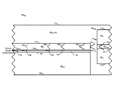
[001.71 With reference to Fig, 1 an optical coupler device 100 is depicted for
transferring light to or from a single mode optical fiber 102 to a silicon-on-
insulator
(S01) waveguide with low loss, though it is understood that any suitable
semiconductor-on-insulator material is within the scope of present
specifications. The
device 100 is understood to be depicted schematically, with the view depicted
representing a cross-section of the device 100, for example through a plane
that
perpendicularly intersects the layers of the device 100 and the optical fiber
102, and in
particular perpendicularly intersects respective optical waveguides of the
device 100
and the optical fiber 102.
100181 The device 100 comprises five optical semiconducting or dielectric
layers: a
substrate 104, a first layer 106 of oxide material, an optical waveguide 108,
a second
layer 110 of oxide material, and an index matching material 112. The layers
are next
described.
100191 An initial layer comprises a substrate 104 comprising a waveguide
material
having a waveguide refractive index RIwo. In some examples, the substrate 104
may
comprise and/or be made of silicon (Si), and may colloquially be referred to
as an SOI
handle.
100201 A first layer 106 of oxide material is "above" and/or on the substrate
104. The
first layer 106 has a first refractive index R11 lower than the waveguide
refractive index
RIwG. The first layer 106 of oxide material may comprise a layer of silicon
oxide (SiO2)
dielectric (e.g. buried insulator oxide). Hence, the first layer 106 of oxide
material may
comprise an oxide of the material of the substrate 104. It is further
understood that
references to one layer (and the like) being "above" another layer, as used
herein, use
the substrate 104 as a bottom-most reference layer; for example, a layer
described
herein may be above another layer presuming the substrate 104 is a lowest
and/or
bottom-most layer,
Date Recue/Date Received 2022-05-05
PCK ATTORNEY DOCKET NO.: P10598CA00
100211 An optical waveguide 108 is generally on the first layer 106 of the
oxide
material, the optical waveguide 108 comprising the waveguide material having
the
waveguide refractive index RIwG. Put another way, the optical waveguide 108
may
comprise the same waveguide material as the substrate 104, and hence may
comprise a
silicon waveguide layer. Furthermore, the optical waveguide 108 may be
referred to as
being "above" or "on" the "buried insulator oxide" of the first layer 106. The
optical
waveguide is understood to be of a cross-sectional shape that is suitable for
guiding
light into and out of the device 100, for example to, or from, one or more
optical
components (not depicted) within the device 100, such as modulators or
demodulators,
and the like. A shape of the optical waveguide 108 is described in more detail
below
with respect to FIG. 2 and FIG. 3. However, it is understood that the optical
waveguide
108 is generally narrower in width than the first layer 106 of the optical
material (e.g_
in a direction into or out of the page of FIG. 1).
100221 A second layer 110 of the oxide material (e.g. the same optical
material as the
first layer 106) is generally on the optical waveguide 108 and the first layer
106 of the
oxide material, the second layer 110 of the oxide material having a second
refractive
index Rh higher than the first refractive index RL and less than the waveguide
refractive index RhvG. Furthermore, the second layer 110 may be thicker than
the first
layer 106, and hence may be referred to as a "thick dielectric" slab waveguide
layer
(e.g. which may comprise a form or doped or undoped SiO2).
100231 The first layer 106 of the oxide material may be referred to as an
undercladding
layer, as the first layer 106 of the oxide material is "under" the optical
waveguide 108
(e.g. with reference to the substrate 104 as a base and/or lowest layer of the
device 100).
Similarly, the second layer 110 of the oxide material may be referred to as an
overcladding layer, as the second layer 110 of the oxide material is "over"
and/or
around the optical waveguide 108. Hence, together, the layers 106, 110
generally act as
cladding layers for the optical waveguide 108, similar to cladding of an
optical fiber.
6
Date Recue/Date Received 2022-05-05
PCK ATTORNEY DOCKET NO.: P10598CA00
However, as will be explained below, light may enter or exit the device 100
via the first
layer 106 of the oxide material.
100241 In general, the first layer 106 of the oxide material, the optical
waveguide 108,
and the second layer 110 of the oxide material generally form an end face 114
for light
coupling, for example with the optical fiber 102. Furthermore, it is
understood that the
optical waveguide 108 extends inwards from the end face 114 (e.g. towards the
optical
components at an interior of the device 100) and that the optical waveguide
108 is
increasing in effective refractive index from the end face 114. Put another
way, the
effective refractive index is understood to be a minimum and/or smallest value
adjacent
the end face 114 (e.g. similar to the refractive index Rh of the second layer
110), and
increases from the end face 114 towards the interior of the device 100 and may
have a
maximum value of the waveguide refractive index RIwci. Such an increase in
effective
refractive index may be achieved via a tapered and/or modulated tapered
structure
described in more detail below with respect to FIG. 2 and FIG. 3.
100251 The index matching material 112 is generally on the second layer 110 of
the
oxide material, and the index matching material 112 generally encapsulates at
least the
second layer 110 of the oxide material and the end face 114. Furthemiore, a
respective
refractive index Rhm of the index matching material 112 is selected to be
about index
matched to the first refractive index Rh I of the first layer 106 of the oxide
material. The
index matching material 112 may comprise any suitable optical epoxy selected
to have
a refractive index that is about index matched to the first refractive index
Rh of the first
layer 106 of the oxide material.
100261 The index matching material 112 may be colloquially referred to as a
super-
cladding layer that encapsulates the other layers of the device 100 and is
generally
understood to further encapsulate a fiber end face 116 of the optical fiber
102, such that
the index matching material 112 acts as a transition optical index material
between the
fiber end face 116 of the optical fiber 102 and the end face 114 of the device
100.
7
Date Recue/Date Received 2022-05-05
PCK ATTORNEY DOCKET NO.: P10598CA00
100271 While the index matching material 112 is depicted as being between the
end
faces 114, 116, and uniformly encapsulating the second layer 110, the index
matching
material 112 may not uniformly encapsulate the second layer 110, but rather
the index
matching material 112 may be thickest in a region between and/or adjacent the
end
faces 114, 116, and taper off in thickness away from the region between and/or
adjacent
the end faces 114, 116. Indeed, the index matching material 112 may have any
suitable
shape and/or physical profile, as long as the index matching material 112
contains light
travelling and/or being conveyed between the end faces 114, 116 and further
assists at
containing light within the layers 106, 110 and the optical waveguide 108
(e.g. without
light leaking out of the index matching material 112 and/or the layers 106,
110 and the
optical waveguide 108).
100281 In particular, control and/or selection of the refractive indices of
the layers 106,
110, and the optical waveguide 108, along with the thickness of the layers
106, 110,
and the optical waveguide 108 may assist with coupling of light into, and out
of., the
device 100.
100291 In general, using silicon as an example, a combination of the substrate
104, the
layers 106, 110, and the optical waveguide 108 may he manufactured by starting
with
the substrate 104 made of silicon, and growing the first layer 106 of the
oxide material,
such as SiO2, on the substrate 104 using any suitable technique (e.g. such as
chemical
vapor deposition (CVD), and the like). A layer of Si may be grown on the first
layer
106 using any suitable technique, and the layer of Si may be suitably etched,
and the
like, to form the optical waveguide 108. The second layer 110 of the oxide
material,
such as SiO2, may be grown on the optical waveguide 108 and the first layer
106 using
any suitable technique (e.g. such as chemical vapor deposition (CVD), and the
like);
for example, as the optical waveguide 108 is narrower then the first layer
106, the
second layer 110 on either side of the optical waveguide 108 (e.g. along an
optical axis
and/or longitudinal axis of the optical waveguide 108) is exposed and, as
such, the
second layer 110 is grown on both the optical waveguide 108 and the first
layer 106.
Date Recue/Date Received 2022-05-05
PCK ATTORNEY DOCKET NO.: P10598CA00
[00301 Ideally, the respective refractive indices Rh, R12 of the layers 106,
110 are the
same or about the same. However, in practice it is challenging using current
manufacturing techniques to achieve this. For example, in the manufacturing
process
described above, the refractive index Rb of the second layer 110 tends to be
higher than
the refractive index RI of the first layer 106.
[00311 This leads to coupling problems when light from the optical fiber 102
is coupled
into the optical waveguide 108_
[00321 For example, in general, the optical fiber 102 may comprise a single
mode
optical fiber, that comprises a cladding layer 118 that is cylindrically
arranged around
a fiber optical waveguide 120 through which light 122 is conveyed. It is
understood
that the refractive index RIc of the cladding layer 11 S is less than the
refractive index
RInvo of the fiber optical waveguide 120 such that total internal reflection
contains the
light 122 within the fiber optical waveguide 120.
[00331 As depicted, the light 122 is being conveyed out of the fiber optical
waveguide
120 and exits the optical fiber 102 at the fiber end face 116. In general, in
prior art
optical couplers, the fiber end face 116 and/or the optical waveguide 120
would be
centered on the optical waveguide 108 of the device 100 and no index matching
material
112 would be present. However, due to the refractive index R12 of the second
layer 110
of oxide material being higher the refractive index RI] of the first layer 106
of oxide
material, when the fiber end face 116 and/or the optical waveguide 120 is
centered on
the optical waveguide 108 of the device 100, the light 122 generally leaks
into the
substrate 104 and may be lost, a situation which is exacerbated by the optical
waveguide
108 being further generally manufactured with an increasing effective
refractive index
(e.g. a tapered structure). While FIG. 1 shows the light 122 exiting the
optical fiber 102
and entering the end face 114, it is understood that the light 122 may exit
the end face
114, and enter the optical fiber 102; however, a similar problem exists in
this situation
when the index matching material 112 is absent.
9
Date Recue/Date Received 2022-05-05
PCK ATTORNEY DOCKET NO.: P10598CA00
100341 The problem may be at least partially addressed by using the second
layer 110
of the oxide material (e.g. the thick dielectric slab waveguide layer) to
couple the light
122 to and from the optical fiber 102. In particular, as the refractive index
Rh of the
second layer 110 is greater than both the refractive index Rh of the first
layer 106 of
the oxide material, and the refractive index Rim of the index matching
material 112,
the second layer 110 of the oxide material effectively acts, at least at the
end face 114,
as an optical waveguide to couple the light 122 into, and out of, the coupler
device 100.
Put another way, at the end face 114, the effective refractive index of the
optical
waveguide 108 is at a minimum and/or at about the refractive index Rh of the
second
layer 110 of the oxide material. Hence, at the end face 114, the light 122
interacts with
the second layer 110 of the oxide material acting as an optical waveguide at a
higher
refractive index Rh, higher than the refractive index Rh of the first layer
106 of the
oxide material and the index matching material 112, which effectively act as
cladding
relative to the second layer 110 of the oxide material. Put another way, at
the end face
114, the combination of the second layer 110 of the oxide material surrounded
by the
first layer 106 of the oxide material and the index matching material 112 form
a similar
optical structure as the optical fiber 102.
100351 Put yet another way, the thick dielectric slab "waveguide" second layer
110
couples light to and from the optical fiber 102, and the refractive index of
the second
layer 110 is generally greater than both the "sub-insulating" dielectric layer
106 and the
super-cladding index matching material 112. Furthermore, the optical waveguide
108
is is shaped to adjust the effective "optical mode" refractive index and
provide a
transition mechanism to couple light into or out of the thick dielectric slab
"waveguide"
second layer 110, to or from the thick dielectric slab "waveguide" second
layer 110.
[0036I For example, as depicted, the light 122 is depicted at different
positions 124,
126, 128, 130 as it travels through the second layer 110. Each subsequent
position 124,
126, 128, 130 is further from the end face 114, and towards the interior of
the device
100 (e.g. towards the internal optical components). Furthermore, at subsequent
position
Date Recue/Date Received 2022-05-05
PCK ATTORNEY DOCKET NO.: P10598CA00
124, 126, 128, 130, the effective refractive index of the optical waveguide
108 is
understood to increase.
[0037] At the first position 124, immediately adjacent the end face 114, the
light 122
has about the same intensity as when entering the end face 114; the light.
However, at
the next position 126, further towards the interior of the device 100, a
portion 132 of
the light has leaked into the optical waveguide 108. At yet a next position
128, yet
further towards the interior of the device 100, a larger portion 134 of the
light has leaked
into the optical waveguide 108. Similarly, at yet a next position 130, yet
further towards
the interior of the device 100, a subsequently larger portion 136 of the light
has leaked
into the optical waveguide 108 until, at yet a further position, all of the
light 122 has
leaked into the optical waveguide 108 as light 138. At the position where the
light 138
is depicted, it is understood that the effective refractive index of the
optical waveguide
108 has increased to the refractive index RIwo of the waveguide material.
Furthermore,
it is understood that the length of the optical waveguide 108 over which the
refractive
index increases from the minimum at the end face 114 to (e.g., at least
approaching) the
refractive index RIwo of the waveguide material is selected to promote the
leaking of a
maximum portion of the light 122 into the optical wavcguidc 108 (though some
loss
may occur). Indeed, the length of the optical waveguide 108 is understood Lobe
selected
such that the light 138 is detectible and/or processible by the optical
components of the
device 100.
100381 It is further understood that the depicted process is reversible. For
example, the
light 138 travelling towards the end face 114 will generally leak into the
second layer
110 and exit the end face 114 at the second layer 110 and into the optical
waveguide
120 of the optical fiber 102. Hence, light can be coupled to and from the
optical fiber
102, and to and from the optical waveguide 108 via the second layer 110.
Hence, it is
further understood that the length of the optical waveguide 108 is understood
to be
selected such that light 138 travelling towards the end face 114, that
generally leaks
into the second layer 110 and exits the end face 114 at the second layer 110
and into
11
Date Recue/Date Received 2022-05-05
PCK ATTORNEY DOCKET NO.: P10598CA00
the optical waveguide 120 of the optical fiber 102, is i detectible and/or
processible by
the optical components that receive such light via the optical fiber 102.
Hence it is
understood that the length of the optical waveguide 108 is any suitable
length, which
may be determined heuristically.
100391 In some examples, the -insulating" index matching material 112 is in a
range of
between about 2 urn to about 3 urn thick, the optical waveguide 108 is in a
range of
between about 100 nm to about 300 inn thick, and the second layer 110 of the
oxide
material is in a range of between about 7 [tm and about! 0 um thick.
Furthermore, the
widths of the optical waveguide 108 and the second layer 110 may be any
suitable
values, which may be determined heuristically to promote leakage therebetween
as
described above. However, it is understood that while certain dimensions are
described
herein for the various components of the device 100, such dimensions are not
meant to
be exhaustive, and functionality of the device 100 as described herein may be
achieved
with other dimensions.
100401 Furthermore, in some examples, the waveguide material and/or the
optical
waveguide 108 may comprise silicon, and the oxide material of the layers 106,
110
may comprise silicon oxide. As such, the refractive index RWG of the waveguide
material of the optical waveguide 108 may be about 3.4 (e.g. the refractive
index of
silicon), the refractive index R2 of the oxide material of the second layer
110 may be in
a range of about 1.44 to about 1.46 (e.g. the refractive index of a doped
silicon oxide),
and the refractive index RI of the oxide material of the first layer 106 arid
the refractive
index Rim/ may each be about in a range of about 1.43 to about 1.45 (e.g. the
refractive
index of silicon oxide). However, it is further understood that the refractive
index RI
of the oxide material of the first layer 106 and the refractive index RIim
also satisfies a
condition of being less than the refractive index R, of the oxide material of
the second
layer 110.
100411 Control of the effective index of the optical waveguide 108 is next
described
with respect to FIG. 2 and FIG. 3.
12
Date Recue/Date Received 2022-05-05
PCK ATTORNEY DOCKET NO.: P10598CA00
100421 For example, FIG. 2 and FIG. 3 each show a "downward" view of examples
of
the optical waveguide 108 and the second layer 110, for example in a direction
of the
substrate 104 perpendicular to an optical axis and/or longitudinal axis of the
optical
waveguide 108. As depicted, the second layer 110 surrounds, and/or is located
on
opposite sides of the optical waveguide 108.
100431 In particular, FIG. 2 depicts a tapered structure of the optical
waveguide 108,
while FIG. 3 depicts a modulated tapered structure of the optical waveguide
108. The
optical waveguide 108 may be manufactured according to either of the depicted
structures, both of which cause the effective refractive index of the optical
waveguide
108 to increase from the end face 114 towards the interior of the device 100.
100441 With reference to FIG. 2, the waveguide material of the optical
waveguide 108
is tapered and increasing in width from the end face 114 inwards_ In
particular, as
depicted, at the end face 114, the waveguide material of the optical waveguide
108 is
at a point and/or tip of the tapering, and towards the interior of the device
100 increases
in width. As such, and as the second layer 110 surrounds, and/or is located on
opposite
sides of the optical waveguide 108 at the end face 114, the effective
refractive index of
the optical waveguide 108 is formed by a combination of the refractive index
RI of the
oxide material of the second layer 110 and the refractive index Rwci of the
waveguide
material of the optical waveguide 108. As the width of the waveguide material
of the
optical waveguide 108 at the end face 114 is at a point, and/or very narrow as
compared
to the respective width of the oxide material of the second layer 110, at the
end face
114, the effective refractive index of the optical waveguide 108 may be about
equal to
the refractive index RI of the oxide material of the second layer 110.
However, as the
width of the waveguide material of the optical waveguide 108 increases, the
contribution to the effective index by the refractive index RWG of the
waveguide
material increases and the effective refractive index of the optical waveguide
108 also
increases to be greater than both the refractive indices RI, R2 of the oxide
material of
the layers 106, 110, Indeed, the effective index of the optical waveguide 108
may
approach, and/or be about equal to, the refractive index Rwci of the waveguide
material,
13
Date Recue/Date Received 2022-05-05
PCK ATTORNEY DOCKET NO.: P10598CA00
for example, as light exits (or enters) the optical waveguide 108 at the
interior of the
device 100 (e.g. to or from the interior optical components).
100451 With reference to FIG. 3, the waveguide material of the optical
waveguide 108
may alternatively have a modulated taper structure, which may have similar
optical
properties as the tapered structure of FIG. 2.
100461 In particular, the modulated taper structure comprises: separated
portions of the
waveguide material extending inwards from the end face 114 for a given length
300;
and thereafter a taper structure extending inwards from the end face 114. Put
another
way, the modulated taper structure is similar to the tapered structure of FIG.
2, but there
are separated portions of the waveguide material between a tip and/or point of
a tapered
structure and the end face 114, the modulated taper structure comprising
separated dots
and/or separated lines of the waveguide material that are aligned along a
longitudinal
axis of the tapered structure. Such a modulated tapered structure may have
similar
optical properties as the tapered structure of FIG. 2, but the effective
refractive index
along the given length 300 may increase less than the effective refractive
index along a
similar length of the tapered structure of FIG. 2.
100471 While two example structured for the optical waveguide 108 are
depicted, it is
understood that any suitable structure for the optical waveguide 108 that
provides an
increasing effective refractive index from the end face 114 is within the
scope of the
present specification.
100481 It is further understood that, regardless of the structure of the
optical waveguide
108, the fiber end face 116 and the optical waveguide 120 of the optical fiber
102 is
about aligned with the second layer 110 of the oxide material, for example
about
centered on the second layer 110 of the oxide material, and adjacent to and/or
"above"
the optical waveguide 108 of the device 100. Indeed, the optical waveguide 120
of the
optical fiber 102 may be aligned with the second layer 110 of the oxide
material, and
about centered on line that is through a center of the optical waveguide 108
and
perpendicular to a longitudinal axis of the optical waveguide 108.
14
Date Recue/Date Received 2022-05-05
PCK ATTORNEY DOCKET NO.: P10598CA00
100491 While such alignment of the optical fiber 102 with the second layer 110
of the
oxide material may occur in any suitable manner, in some examples, and with
reference
to FIG. 4, which schematically shows a perspective view of the device 100 and
the
optical fiber 102 being assembled, the device 100 may comprise an alignment
structure
400, extending outward from the end face 114 (e.g. away from the interior of
the device
100 and/or towards an exterior edge 402 of the device 100), the alignment
structure 400
configured to about center the fiber end face 116 of the optical fiber 102
with the
second layer 110 of the oxide material at the end face 114, such that light
from the
optical fiber 102 enters the second layer 110 of the oxide material at the end
face 114,
or respective light from the second layer 110 of the oxide material enters the
optical
fiber 102 at the fiber end face 116.
100501 It is further understood that only a portion of optical fiber 102 is
depicted in FIG_
4, and the optical fiber 102 may extends out of the page of FIG. 4 for tens,
hundreds or
thousands of meters, or more. Furthermore, FIG. 4 only depicts a portion of
the device
100, which may include a plurality of optical waveguides 108, etc., with a
plurality of
corresponding alignment structures 400, to interface with a plurality of
optical fibers
102.
100511 In particular, FIG. 4 further graphically depicts a method to assemble
the optical
fiber 102 and the device 100. For example, an end the optical fiber 102 that
includes
the fiber end face 116, is lowered and/or placed into the alignment structure
400, and
the alignment structure has a shape that, when end the optical fiber 102 that
includes
the fiber end face 116 is lowered and/or placed into the alignment structure
400, the
alignment described with respect to FIG. 1 is achieved (e.g. the optical
waveguide 120
of the optical fiber 102 is aligned with the second layer 110 of the oxide
material at the
end face 114).
100521 FIG. 4 further shows that the index matching material 112, for example
in the
form of an optical epoxy, may be used to attach the optical fiber 102 to the
device 100,
and fill the region between the end faces 114, 116, as well as cover the
second layer
110. However, any suitable combination of the index matching material 112 and
Date Recue/Date Received 2022-05-05
PCK ATTORNEY DOCKET NO.: P10598CA00
another epoxy, and the like, may be used to attach the optical fiber 102 to
the device
100.
[00531 In particular, as depicted, and the alignment structure 400 may
comprise a V-
shaped groove extending outwards from the end face 114, which may be formed
from
the material of the substrate 104, which may extend outward from the end face
114 to
the depicted edge 402, with the layers 106, 110 and the optical waveguide 108
grown
on the substrate 104 adjacent the alignment structure 400, though the
alignment
structure 400 may be formed before or after formation of the layers 106, 110
and the
optical waveguide 108, and/or at any suitable point in the manufacturing of
the device
100. In particular, the V- shaped groove of the alignment structure 400 may
etched into
the substrate 104.
100541 An end view of the V- shaped groove of the alignment structure 400 is
fiwther
depicted in FIG. 5, after assembly of the device 100 and the optical fiber
102, the view
of the V- shaped groove of the alignment structure 400 being along an optical
axis of
the optical waveguide 120 of the optical fiber 102. Components of the optical
fiber 102
are depicted as being transparent to show their positions relative to the
components of
the device 100.
[00551 As clearly seen in FIG. 5, sides of the optical fiber 102 are resting
and/or held
into place in the V- shaped groove of the alignment structure 400 (e.g. by the
optical
epoxy of the index matching material 112, and/or another epoxy, and the like),
such to
achieve the alignment between the optical waveguide 120 of the optical fiber
102 and
the second layer 110 of the oxide material. As such, it is understood that
slopes of sides
of the V- shaped groove of the alignment structure 400, and a depth of the V-
shaped
groove of the alignment structure 400 are selected to achieve such alignment.
[01)561 FIG. 5 further shows that the optical waveguide 120 of the optical
fiber 102 is
aligned with the second layer 110 of the oxide material, and about centered on
a line
500 that is through a center of the optical waveguide 108 and perpendicular to
a
longitudinal axis of the optical waveguide 108 (e.g. which is understood to be
normal
to the page of FIG. 5).
16
Date Recue/Date Received 2022-05-05
PCK ATTORNEY DOCKET NO.: P10598CA00
[0057] FIG. 5 further shows that the index matching material 112 may have any
suitable shape on the optical fiber 102 and the second layer 110.
[0058] Attention is next directed to FIG. 6 which depicts a method 600 for
manufacturing a waveguide coupler device, such as the device 100 combined with
the
optical fiber 102.
[0059] At a block 602, the device 100 is provided, the device 100 comprising:
[0060] -a substrate 104 comprising a waveguide material having a waveguide
refractive
index;
[0061] -a first layer 106 of oxide material on the substrate 104 having a
first refractive
index lower than the waveguide refractive index;
[0062] -an optical waveguide 108 on the first layer of the oxide material, the
optical
waveguide 108 comprising the waveguide material having the waveguide
refractive
index;
[0063] -a second layer 110 of the oxide material on the optical waveguide 108
and the
first layer 106 of the oxide material, the second layer 110 of the oxide
material having
a second refractive index higher than the first refractive index and less than
the
waveguide refractive index, the first layer 106 of the oxide material, the
second layer
110 of the oxide material, and the optical waveguide 108 forming the end face
114 for
light coupling, and the optical waveguide 108 extending inwards from the end
face 114
and increasing in effective refractive index from the end face 114.
[0064) In particular, the device 100 may be manufactured using any suitable
combination of deposition techniques, etching techniques and the like.
[0065] At a block 604, an alignment structure 400 is formed at the device 100
extending
outward from the end face 114, the alignment structure 400 configured to about
center
a fiber end face 116 of an optical fiber 102 with the second layer 110 of the
oxide
material at the end face 114, such that light from the optical fiber 102
enters the second
layer 110 of the oxide material at the end face 114, or respective light from
the second
layer 110 of the oxide material enters the optical fiber 102 at the fiber end
face 116.
17
Date Recue/Date Received 2022-05-05
PCK ATTORNEY DOCKET NO.: P10598CA00
100661 The alignment structure 400 may comprises a V-shaped groove extending
outwards from the end face 114, for example formed via etching in the
substrate 104.
100671 As any suitable alignment structure and/or method of alignment is
within the
scope of the present specification, the block 604 may be optional.
100681 At a block 606, the fiber end face 116 of the optical fiber 102 is
aligned and/or
centered with the second layer 110 of the oxide material at the end face 114.
As any
suitable alignment structure and/or method of alignment is within the scope of
the
present specification, the block 606 may also be optional and/or inherent an
inherent
component of the block 602 and/or the block 604.
100691 At a block 608, at least the second layer 110 of the oxide material and
the end
face 114 are encapsulated with the index matching material 112, a respective
refractive
index of the index matching material 112 being about index matched to the
first
refractive index of the first layer 110. In particular, the index matching
material 112
may fill any gap between the end faces 114, 116, and further encapsulates that
portion
of the second layer 110 where light is travelling therethrough, as described
above with
respect to FIG. 5.
100701 In this specification, elements may be described as "configured to"
perform one
or more functions or "configured for" such functions. In general, an element
that is
configured to perform or configured for performing a function is enabled to
perform
the function, or is suitable for performing the function, or is adapted to
perform the
function, or is operable to perform the function, or is otherwise capable of
performing
the function.
100711 It is understood that for the purpose of this specification, language
of "at least
one of X, Y, and Z" and "one or more of X, Y and Z" can be construed as X
only, Y
only, Z only, or any combination of two or more items X, Y, and Z (e.g., XYZ,
XY,
YZ, XZ, and the like). Similar logic can be applied for two or more items in
any
occurrence of "at least one..." and "one or more..." language.
100721 The terms "about", "substantially", "essentially", "approximately", and
the like,
are defined as being "close to", for example as understood by persons of skill
in the art.
18
Date Recue/Date Received 2022-05-05
PCK ATTORNEY DOCKET NO.: P10598CA00
In some examples, the terms are understood to be "within 10%," in other
examples,
"within 5%", in yet further examples, "within I %", and in yet further
examples "within
0.5%".
100731 Persons skilled in the art will appreciate that there are yet more
alternative
examples and modifications possible, and that the above examples are only
illustrations
of one or more embodiments. The scope, therefore, is only to be limited by the
claims
appended hereto.
19
Date Recue/Date Received 2022-05-05