Note: Descriptions are shown in the official language in which they were submitted.
WO 2021/097561
PCT/CA2020/051563
1
ULTRASONIC TRANSDUCERS, BACKING STRUCTURES AND RELATED METHODS
TECHNICAL FIELD
The technical field generally relates to the field of acoustic energy and more
particularly relates to an
ultrasonic transducer, related devices, apparatuses methods and techniques.
BACKGROUND
Piezoelectric acoustic transducers are widely used in many industries and for
a broad variety of applications.
For example, piezoelectric ultrasonic transducers can be employed in medical
applications, for example
diagnostic imaging and/or therapeutic applications. Other applications include
but are not limited to
ultrasonic non-destructive testing and ultrasonic machining and welding.
Piezoelectric ultrasonic
transducers change electrical energy into mechanical energy, and reciprocally
convert acoustic waves into
electrical signal(s).
There is still a need for techniques, apparatus, devices and methods that
alleviate or mitigate the problems
of prior art.
SUMMARY
In accordance with one aspect, there is provided an ultrasonic transducer,
including:
a piezoelectric material having a front surface and a back surface, the
piezoelectric material being
configured to be in acoustic communication with a sample;
a backing structure positioned at the back surface of the piezoelectric
material and configured to
reflect acoustic energy towards the front surface of the piezoelectric
material, the backing structure
being thermally conductive and electrically conductive, the backing structure
including:
a first dual layer de-matching backing, the first dual layer de-matching
backing including:
a first layer of graphite, and
a layer made of tungsten in contact with the first layer of graphite;
a second dual layer de-matching backing contacting the first dual layer de-
matching backing,
the second dual layer de-matching backing including:
a second layer of graphite; and
CA 03158819 2022-5-18
WO 2021/097561
PCT/CA2020/051563
2
a layer of copper in contact with the second layer of graphite;
a heat sink in thermal contact with the backing structure; and
one or more electrodes in electrical communication with the piezoelectric
material.
In some embodiments, the heat sink includes at least one channel, the channel
being configured for receiving
6 and circulating a heat transfer fluid therein.
In some embodiments, the heat transfer fluid is a liquid_
In some embodiments, the heat sink is electrically insulated from the backing
structure.
In some embodiments, the ultrasonic transducer is operable at an operational
frequency, the operational
frequency being related to an operational wavelength (A.,); and the layer of
graphite, the layer made of
tungsten in contact with the first layer of graphite, the second layer of
graphite and the layer of copper each
have a corresponding thickness of about La thick or odd multiples of A../4.
In some embodiments, the piezoelectric material is configured to be half wave
resonant at the operational
frequency.
In some embodiments, the ultrasonic transducer includes a single de-matching
layer positioned between the
piezoelectric material and the backing structure, the single de-matching layer
being in acoustic
communication with the piezoelectric material and the backing structure, the
single de-matching layer
having a corresponding acoustic impedance relatively higher than an acoustic
impedance of the piezoelectric
material, wherein the piezoelectric material is configured to be quarter wave
resonant at the operational
frequency.
In some embodiments, the piezoelectric material has a resonant frequency, the
resonant frequency being
related to a resonant wavelength A.õ., the single de-matching layer having a
thickness of less than 22415 thick
with respect to the resonant frequency of the piezoelectric material.
In some embodiments, the single de-matching layer has a Thickness ranging
between about Ad10 and about
)1/44/20.
In some embodiments, the single de-matching layer is made from tungsten_
In some embodiments, the piezoelectric material has acousting properties
including an acoustic impedance
of about 27.5 Megartayls.
CA 03158819 2022-5-18
WO 2021/097561
PCT/CA2020/051563
3
In some embodiments, the first layer of graphite has an acoustic impedance of
about 5.1 MegaRayls.
In some embodiments, the first layer of graphite has a thickness included in a
range extending from about
1.5 min to about 1.6 rum.
In some embodiments, the layer of tungsten has an acoustic impedance of about
100 MegaRayls.
6 In some embodiments, the layer of tungsten has a thickness included in a
range extending from about 2.6
mm to about 2.7 min_
In some embodiments, the second layer of graphite has an acoustic impedance of
about 5.1 MegaRayls.
In some embodiments, the second layer of graphite has a thickness included in
a range extending from about
1.5 mm to about 1.6 mm.
In some embodiments, the layer of copper has an acoustic impedance of about
41.5 MegaRayls.
In some embodiments, the layer of copper has a thickness included in a range
extending from about 2.5 mm
to about 2.6 mm.
In some embodiments, the piezoelectric material is a poled composite
piezoelectric disc.
In some embodiments, the poled composite piezoelectric disc is in a 1 3
configuration.
In some embodiments, the piezoelectric material is a composite of PZT4, the
piezoelectric material
including 1000 urn by 1000 urn pillars separated by 200 urn kerfs, the kerfs
being cut at a pitch of about
1200 urn.
In some embodiments, the piezoelectric material has a thickness included in a
range extending from about
2.35 min to about 2.45 mm.
In some embodiments, the kerfs are filled with a composite filler, the
composite filler including particles of
hafnium dioxide doped into epoxy.
In some embodiments, the composite filler is in a 0 3 configuration.
In some embodiments, the epoxy is Epo-Tek 301.
In some embodiments, the piezoelectric material consists of a piezoelectric
layer.
CA 03158819 2022-5-18
WO 2021/097561
PCT/CA2020/051563
4
In some embodiments, the ultrasonic transducer includes a thermally conductive
structure in contact with
the backing structure.
In some embodiments, the thermally conductive structure is electrically
insulated from the backing
structure.
In some embodiments, the thermally conductive structure is a layer made of AIN
or a layer made of
beryllium oxide.
In some embodiments, the thermally conductive structure extends on lateral
portions of the backing
structure.
In some embodiments, the thermally conductive structure includes at least one
electrically conductive via
passing through the -thermally conductive structure.
In some embodiments, the ultrasonic transducer includes a control unit
electrically connected to at least one
of the piezoelectric material, the backing structure and the one or more
electrodes.
In some embodiments, the one or more electrodes are electrically connected to
the piezoelectric material
through the backing structure.
In some embodiments, the ultrasonic transducer includes a wear layer having
abrasion-resistant properties.
In some embodiments, the wear layer is made from titanium.
In some embodiments, the ultrasonic transducer has a diameter of about 50 mm.
In some embodiments, the backing structure is further configured to reflect
the acoustic energy in phase.
In some embodiments, the backing structure is further configured to spatially
and temporally disperse
unwanted acoustic reverberations in the backing structure.
In accordance with one aspect, there is provided an ultrasonic transducer,
including:
a piezoelectric material having a front surface and a back surface, the
piezoelectric material being
configured to be in acoustic communication with a sample; and
a backing structure positioned at the back surface of the piezoelectric
material and configured to
reflect acoustic energy towards the front surface of the piezoelectric
material, the backing structure
including:
CA 03158819 2022-5-18
WO 2021/097561
PCT/CA2020/051563
a first dual layer de-matching backing, the first dual layer de-matching
backing including a first
low acoustic impedance layer and a first high acoustic impedance layer, and
a second dual layer de-matching backing connected to the first dual layer de-
matching backing,
the second dual layer de-matching backing including a second low acoustic
impedance layer and
5 a second high acoustic impedance layer_
In some embodiments, the ultrasonic transducer includes at least one of a heat
sink in thermal contact with
the backing structure or a thermally conductive layer acoustically matched
with the piezoelectric material.
hi some embodiments, the ultrasonic transducer includes one or more electrodes
in electrical communication
with the piezoelectric material.
In some embodiments, the backing structure is thermally conductive and
electrically conductive_
In some embodiments, the ultrasonic transducer includes a pre-assembled
electrical circuit, the pre-
assembled electrical circuit being in electrical communication with a top
portion of the backing structure,
such that it is in electrical communication with the piezoelectric material.
In some embodiments, the pm-assembled electrical circuit includes at least one
of: a printed circuit board,
an interposer, an integrated circuit and an application-specific integrated
circuit.
In some embodiments, the heat sink includes at least one channel, the channel
being configured for receiving
and circulating a heat transfer fluid therein.
In some embodiments, the heat transfer fluid is a liquid.
In some embodiments, the heat sink is electrically insulated from the backing
structure.
hi some embodiments, the ultrasonic transducer is operable at an operational
frequency, the operational
frequency being related to an operational wavelength (A.); and the first low
acoustic impedance layer, the
first high acoustic impedance layer, the second low acoustic impedance layer
and the second high acoustic
impedance layer each have a corresponding thickness of about A.0/4 thick or
odd multiples of X.,J4.
In some embodiments, the piezoelectric material is configured to be half wave
resonant at the operational
frequency.
In some embodiments, the ultrasonic transducer includes a single de-matching
layer positioned between the
piezoelectric material and the backing structure, the single de-matching layer
being in acoustic
CA 03158819 2022-5-18
WO 2021/097561
PCT/CA2020/051563
6
communication with the piezoelectric material and the backing structure, the
single de-matching layer
having a corresponding acoustic impedance relatively higher than an acoustic
impedance of the piezoelectric
material, wherein the piezoelectric material is configured to be quarter wave
resonant at the operational
frequency.
In some embodiments, the piezoelectric material has a resonant frequency, the
resonant frequency being
related to a resonant wavelength Ac, the single de-matching layer having a
thickness of less than 2k15 thick
with respect to the resonant frequency of the piezoelectric material.
In some embodiments, the single de-matching layer has a thickness ranging
between about XJ10 and about
A120.
In some embodiments, the single de-matching layer is made from tungsten.
In some embodiments, the piezoelectric material has acoustic properties
including an acoustic impedance
of about 27.5 MegaRayls.
In some embodiments, the piezoelectric material is a poled composite
piezoelectric disc.
In some embodiments, the poled composite piezoelectric disc has a thickness of
about 2.4 mm.
In some embodiments, the poled composite piezoelectric disc is in a 1 3
configuration.
In some embodiments, the piezoelectric material is a composite of PZT4, the
piezoelectric material
including 1000 urn by 1000 um pillars separated by 200 urn kerfs, the kerfs
being cut at a pitch of about
1200 urn.
In some embodiments, the kerfs are filled with a composite filler, the
composite filler including particles of
hafnium dioxide doped into epoxy.
In some embodiments, the composite filler is in a 0 3 configuration.
In some embodiments, the epoxy is Epo-Tek 40 301.
In some embodiments, the piezoelectric material consists of a piezoelectric
layer.
In some embodiments, the ultrasonic transducer includes a thermally conductive
structure in contact with
the backing structure.
CA 03158819 2022-5-18
WO 2021/097561
PCT/CA2020/051563
7
In some embodiments, the thermally conductive structure is electrically
insulated from the backing
structure.
In some embodiments, the thermally conductive structure is a layer made of AIN
or a layer made of
beryllium oxide.
In some embodiments, the thermally conductive structure extends on lateral
portions of the backing
structure.
In some embodiments, the thermally conductive structure includes at least one
electrically conductive via
passing through the thermally conductive structure.
hi some embodiments, the ultrasonic transducer includes a control unit
electrically connected to at least one
of the piezoelectric material and the backing structure.
In some embodiments, the one or more electrodes are electrically connected to
the piezoelectric material
through the backing structure.
In some embodiments, the ultrasonic transducer includes a wear layer having
abrasion-resistant properties.
In some embodiments, the wear layer is made from titanium.
In some embodiments, the ultrasonic transducer has a diameter of about 50 mm.
In some embodiments, the backing structure is further configured to reflect
the acoustic energy in phase.
In some embodiments, the backing structure is further configured to spatially
and temporally disperse
unwanted acoustic reverberations in the backing structure.
In accordance with one aspect, there is provided an ultrasonic transducer
having a sample-contacting portion
and a back portion, the back portion being opposed to the sample contacting
portion, including:
a piezoelectric material configured to be in acoustic communication with a
sample; and
a backing structure in acoustic communication with the piezoelectric material,
the backing structure
being configured to reflect acoustic energy towards the sample-contacting
portion and away from the
back portion of the ultrasonic transducer, the backing structure including:
a low acoustic impedance layer; and
a high acoustic impedance layer.
CA 03158819 2022-5-18
WO 2021/097561
PCT/CA2020/051563
8
In some embodiments, the low acoustic impedance layer and the high acoustic
impedance layer form a first
dual layer de-matching backing, and the ultrasonic transducer the ultrasonic
transducer includes a second
dual layer de-matching backing, the second dual layer de-matching backing
including a second low acoustic
impedance layer and a second high acoustic impedance layer.
In some embodiments, the ultrasonic transducer includes a heat sink in thermal
contact with the backing
structure.
In some embodiments, the ultrasonic transducer includes one or more electrodes
in electrical communication
with the piezoelectric material.
In some embodiments, the backing structure is thermally conductive and
electrically conductive.
In some embodiments, the ultrasonic transducer includes a pre-assembled
electrical circuit, the pre-
assembled electrical circuit being in electrical communication with a top
portion of the backing structure,
such that it is in electrical communication with the piezoelectric material.
In some embodiments, the pre-assembled electrical circuit includes at least
one of a printed circuit board,
an interposer, an integrated circuit and an application-specific integrated
circuit.
In some embodiments, the heat sink includes at least one channel, the channel
being configured for receiving
and circulating a heat transfer fluid therein.
In some embodiments, the heat transfer fluid is a liquid.
In some embodiments, the heat sink is electrically insulated from the backing
structure.
In some embodiments, the ultrasonic transducer is operable at an operational
frequency, the operational
frequency being related to an operational wavelength (1.0); and the low
acoustic impedance layer, the high
acoustic impedance layer, the second low acoustic impedance layer and the
second high acoustic impedance
layer each have a corresponding thickness of about X0/4 thick or odd multiples
of ko/4.
In some embodiments, the piezoelectric material is configured to be half wave
resonant at the operational
frequency.
In some embodiments, the ultrasonic transducer includes a single de-matching
layer positioned between the
piezoelectric material and the backing structure, the single de-matching layer
being in acoustic
communication with the piezoelectric material and the bathing structure, the
single de-matching layer
having a corresponding acoustic impedance relatively higher than an acoustic
impedance of the piezoelectric
CA 03158819 2022-5-18
WO 2021/097561
PCT/CA2020/051563
9
material, wherein the piezoelectric material is configured to be quarter wave
resonant at the operational
frequency.
In some embodiments, the piezoelectric material has a resonant frequency, the
resonant frequency being
related to a resonant wavelength 1.,r, the single de-matching layer having a
thickness of less than 2115 thick
with respect to the resonant frequency of the piezoelectric material.
In some embodiments, the single de-matching layer has a thickness ranging
between about 4/10 and about
1120.
In some embodiments, the single de-matching layer is made from tungsten.
In some embodiments, the piezoelectric material has acoustic properties
including an acoustic impedance
of about 27.5 MegaRayls.
In some embodiments, the piezoelectric material is a poled composite
piezoelectric disc.
In some embodiments, the poled composite piezoelectric disc has a thickness of
about 24 mm.
In some embodiments, the poled composite piezoelectric disc is in a 1 3
configuration.
hi some embodiments, the piezoelectric material is PZT4, the piezoelectric
material including 1000 urn by
1000 um pillars separated by 200 um kerfs, the kerfs being cut at a pitch of
about 1200 urn.
In some embodiments, the kerfs are filled with a composite filler, the
composite filler including particles of
hafnium dioxide doped into epoxy.
In some embodiments, the composite filler is in a 0 3 configuration.
In some embodiments, the epoxy is Epo-Tek 301.
In some embodiments, the piezoelectric material consists of a piezoelectric
layer.
In some embodiments, the ultrasonic transducer includes a thermally conductive
structure in contact with
the backing structure.
In some embodiments, the thermally conductive structure is electrically
insulated from the backing
structure.
In some embodiments, the thermally conductive structure is a layer made of AIN
or a layer made of
bervilliun nxicle_
CA 03158819 2022-5-18
WO 2021/097561
PCT/CA2020/051563
In some embodiments, the thermally conductive structure extends on lateral
portions of the backing
structure.
In some embodiments, the thermally conductive structure includes at least one
electrically conductive via
passing through the thermally conductive structure.
5 In some embodiments, the ultrasonic transducer includes a control unit
electrically connected to at least one
of the piezoelectric material and the backing structure.
In some embodiments, the one or more electrodes are electrically connected to
the piezoelectric material
through the backing structure.
In some embodiments, the ultrasonic transducer includes a wear layer having
abrasion-resistant properties.
10 In some embodiments, the wear layer is made from titanium.
In some embodiments, the ultrasonic transducer has a diameter of about 50 mm.
In some embodiments, the backing structure is further configured to reflect
the acoustic energy in phase.
In some embodiments, the backing structure is further configured to spatially
and temporally disperse
unwanted acoustic reverberations in the backing structure.
In some embodiments, the piezoelectric material is diced into a plurality of
piezoelectric regions, separated
one from another by gaps, the gaps being electrically insulating and
acoustically insulating; at least one of
the low acoustic impedance layer and the high acoustic impedance layer is
diced into a first plurality of
elements, separated one from another by a first set of gaps, each of the first
set of gaps being aligned with a
corresponding one of the gaps separating the piezoelectric regions, the first
set of gaps being electrically
insulating and acoustically insulating; and at least one of the second low
acoustic impedance layer and the
second high acoustic impedance layer is diced into a second plurality of
elements, separated one from
another by a second set of gaps, each of the second set of gaps being aligned
with a corresponding one of
the gaps separating the piezoelectric regions, the second set of gaps being
electrically insulating and
acoustically insulating.
In some embodiments, the gaps, the first set of gaps and the second set of
gaps are thermally conductive.
In accordance with one aspect, there is provided an ultrasonic transducer,
including:
CA 03158819 2022-5-18
WO 2021/097561
PCT/CA2020/051563
11
a one-dimensional piezoelectric array haying a front surface and a back
surface, the one-dimensional
piezoelectric may being configured to be in acoustic communication with a
sample and including a
plurality of piezoelectric regions arrayed in one dimension;
a backing structure positioned at the back surface of the one-dimensional
piezoelectric array and
configured to reflect acoustic energy towards the front surface of the one-
dimensional piezoelectric
array, the backing structure including a dual layer de-matching backing, the
dual layer de-matching
backing including a low acoustic impedance layer and a high acoustic impedance
layer; and
a pm-assembled electrical circuit, the pre-assembled electrical circuit being
in electrical
communication with a top portion of the backing structure, such that it is in
electrical communication
with the one-dimensional piezoelectric array.
In some embodiments, the ultrasonic transducer includes a second dual layer de-
matching backing, the
second dual layer de-matching backing including a second low acoustic
impedance layer and a second high
acoustic impedance layer.
In some embodiments, the ultrasonic transducer includes a heat sink in thermal
contact with the backing
structure.
In some embodiments, the ultrasonic transducer includes one or more electrodes
in electrical communication
with the one-dimensional piezoelectric array.
In some embodiments, the backing structure is thermally conductive and
electrically conductive.
In some embodiments, the pre-assembled electrical circuit includes at least
one of a printed circuit board,
an interposer, an integrated circuit and an application-specific integrated
circuit.
In some embodiments, each piezoelectric region is separated one from another
by gaps, the gaps being
electrically insulating and acoustically insulating.
In some embodiments, at least one of the low acoustic impedance layer and the
high acoustic impedance
layer is diced into a first plurality of elements, separated one from another
by a first set of gaps, each of the
first set of gaps being aligned with a corresponding one of the gaps
separating the piezoelectric regions, the
first set of gaps being electrically insulating and acoustically insulating
In some embodiments, at least one of the second low acoustic impedance layer
and the second high acoustic
impedance layer is diced into a second plurality of elements, separated one
from another by a second set of
CA 03158819 2022-5-18
WO 2021/097561
PCT/CA2020/051563
12
gaps, each of the second set of gaps being aligned with a corresponding one of
the gaps separating the
piezoelectric regions, the second set of gaps being electrically insulating
and acoustically insulating.
In some embodiments, the gaps, the first set of gaps and the second set of
gaps are thermally conductive.
In some embodiments, the top portion of the backing structure is made from an
electrically insulating
material.
In some embodiments, wherein the electrically insulating material is thermally
conductive.
In some embodiments, the top portion includes a layer made from AIN traversed
by electrically conductive
vias, each electrically conductive via being aligned to a corresponding one of
the plurality of piezoelectric
regions arrayed in one dimension.
In some embodiments, The layer made from AIN layer has a front face, the layer
made from AIN layer being
partially diced from the front face to enhance acoustic separation of adjacent
ones of the plurality of
piezoelectric regions arrayed in one dimension.
In some embodiments, the heat sink includes at least one channel, the channel
being configured for receiving
and circulating a heat transfer fluid therein.
In some embodiments, the heat transfer fluid is a liquid.
In some embodiments, the heat sink is electrically insulated from the backing
structure.
In some embodiments, the ultrasonic transducer is operable at an operational
frequency, the operational
frequency being related to an operational wavelength (14; and the low acoustic
impedance layer, the high
acoustic impedance layer, the second low acoustic impedance layer and the
second high acoustic impedance
layer each have a corresponding thickness of about X./4 thick or odd multiples
of ),../4.
In some embodiments, the one-dimensional piezoelectric array is configured to
be half wave resonant at the
operational frequency.
In some embodiments, the ultrasonic transducer includes a single de-matching
layer positioned between the
one-dimensional piezoelectric array and the backing structure, the single de-
matching layer being in acoustic
communication with The one-dimensional piezoelectric array and the backing
structure, the single de-
matching layer having a corresponding acoustic impedance relatively higher
than an acoustic impedance of
the one-dimensional piezoelectric array, wherein the one-dimensional
piezoelectric array is configured to
be quarter wave resonant at the operational frequency.
CA 03158819 2022-5-18
WO 2021/097561
PCT/CA2020/051563
13
In some embodiments, the one-dimensional piezoelectric army has a resonant
frequency, the resonant
frequency being related to a resonant wavelength )i-r, the single de-matching
layer having a thickness of less
than 2A15 thick with respect to the resonant frequency of the one-dimensional
piezoelectric array.
In some embodiments, the single de-matching layer has a Thickness ranging
between about kg/10 and about
Xr/20.
In some embodiments, the single de-matching layer is made from tungsten.
In some embodiments, the piezoelectric regions include pillars separated by
kerfs.
In some embodiments, the kerfs are filled with a composite filler, the
composite filler including particles of
hafnium dioxide doped into epoxy
In some embodiments, the composite filler is in a 0 3 configuration.
In some embodiments, the epoxy is Epo-Tek(10 301.
In some embodiments, the piezoelectric regions consist of a piezoelectric
layer.
In some embodiments, the ultrasonic transducer includes a thermally conductive
structure in contact with
the backing structure.
In some embodiments, the thermally conductive structure is electrically
insulated from the backing
structure.
In some embodiments, the thermally conductive structure is a layer made of
MINI or a layer made of
beryllium oxide.
In some embodiments, the thermally conductive structure extends on lateral
portions of the backing
structure.
In some embodiments, the ultrasonic transducer includes a control unit
electrically connected to at least one
of the one-dimensional piezoelectric array and the backing structure.
In some embodiments, the one or more electrodes are electrically connected to
the one-dimensional
piezoelectric array through the backing structure.
In some embodiments, the ultrasonic transducer includes a wear layer having
abrasion-resistant properties.
In come embodiments, the wear layer is made from titanium.
CA 03158819 2022-5-18
WO 2021/097561
PCT/CA2020/051563
14
In some embodiments, the ultrasonic transducer has a diameter of about 50 mm.
In some embodiments, the backing structure is further configured to reflect
the acoustic energy in phase.
In some embodiments, the backing structure is further configured to spatially
and temporally disperse
unwanted acoustic reverberations in the backing structure.
6 ht accordance with one aspect, there is provided an ultrasonic
transducer, including:
a two-dimensional piezoelectfic matrix having a front surface and a back
surface, the two-
dimensional piezoelectric matrix being configured to be in acoustic
communication with a sample;
a backing structure positioned at the back surface of the one-dimensional
piezoelectric matrix and
configured to reflect acoustic energy towards the front surface of the two-
dimensional piezoelectric
matrix, the backing structure including a dual layer de-matching backing, the
dual layer de-matching
backing including a low acoustic impedance layer and a high acoustic impedance
layer; and
a pre-assembled electrical circuit, the pre-assembled electrical circuit being
in electrical
communication with atop portion of the backing structure, such that it is in
electrical communication
with the two-dimensional piezoelectric matrix.
In some embodiments, the ultrasonic transducer includes a second dual layer de-
matching backing, the
second dual layer de-matching backing including a second low acoustic
impedance layer and a second high
acoustic impedance layer.
In some embodiments, the ultrasonic transducer includes a heat sink in thermal
contact with the backing
structure.
In some embodiments, the ultrasonic transducer includes one or more electrodes
in electrical communication
with the two-dimensional piezoelectric matrix.
hi some embodiments, the backing structure is thermally conductive and
electrically conductive.
In some embodiments, the pre-assembled electrical circuit includes at least
one of: a printed circuit board,
an interposer, an integrated circuit and an application-specific integrated
circuit.
In some embodiments, the two-dimensional piezoelectric matric includes a
plurality of piezoelectric regions,
each piezoelectric region being separated one from another by gaps, the gaps
being electrically insulating
and acoustically insulating.
CA 03158819 2022-5-18
WO 2021/097561
PCT/CA2020/051563
In some embodiments, at least one of the low acoustic impedance layer and the
high acoustic impedance
layer is diced into a first plurality of elements, separated one from another
by a first set of gaps, each of the
first set of gaps being aligned with a corresponding one of the gaps
separating the piezoelectric regions, the
first set of gaps being electrically insulating and acoustically insulating
5 In some embodiments, at least one of the second low acoustic impedance
layer and the second high acoustic
impedance layer is diced into a second plurality of elements, separated one
from another by a second set of
gaps, each of the second set of gaps being aligned with a corresponding one of
the gaps separating the
piezoelectric regions, the second set of gaps being electrically insulating
and acoustically insulating.
In some embodiments, the gaps, the first set of gaps and the second set of
gaps are thermally conductive.
10 In some embodiments, the top portion of the backing structure is made
from an electrically insulating
material.
In some embodiments, the electrically insulating material is thermally
c,onductive.
In some embodiments, the top portion includes a layer made from AIN traversed
by electrically conductive
vias, each electrically conductive via being aligned to a corresponding one of
the plurality of piezoelectric
15 regions.
In some embodiments, the layer made from AlN layer has a front face, the layer
made hum AIN layer being
partially diced from the front face to enhance acoustic separation of adjacent
ones of the plurality of
piezoelectric regions arrayed in one dimension.
In some embodiments, the heat sink includes at least one channel, the channel
being configured for receiving
and circulating a heat transfer fluid therein.
In some embodiments, the heat transfer fluid is a liquid.
In some embodiments, the heat sink is electrically insulated from the backing
structure.
In some embodiments, the ultrasonic transducer is operable at an operational
frequency, the operational
frequency being related to an operational wavelength (14; and the low acoustic
impedance layer, the high
acoustic impedance layer, the second low acoustic impedance layer and the
second high acoustic impedance
layer each have a corresponding thickness of about 2so/4 thick or odd
multiples of A.0/4.
In some embodiments, the two-dimensional piezoelectric matrix is configured to
be half wave resonant at
the operational frequency.
CA 03158819 2022-5-18
WO 2021/097561
PCT/CA2020/051563
16
In some embodiments, the ultrasonic transducer includes a single de-matching
layer positioned between the
two-dimensional piezoelectric matrix and the backing structure, the single de-
matching layer being in
acoustic communication with the two-dimensional piezoelectric matrix and the
backing structure, the single
de-matching layer having a corresponding acoustic impedance relatively higher
than an acoustic impedance
of the two-dimensional piezoelectric matrix, wherein the two-dimensional
piezoelectric matrix is configured
to be quarter wave resonant at the operational frequency. .
In some embodiments, the two-dimensional piezoelectric matrix has a resonant
frequency, the resonant
frequency being related to a resonant wavelength 1r, the single de-matching
layer haying a thickness of less
than 2k,./5 thick with respect to the resonant frequency of the two-
dimensional piezoelectric matrix.
In some embodiments, the single de-matching layer has a thickness ranging
between about kr/10 and about
in/20.
In some embodiments, the single de-matching layer is made from tungsten.
In some embodiments, the two-dimensional piezoelectric matrix includes pillars
separated by kerfs.
In some embodiments, the kerfs are filled with a composite filler, the
composite filler including particles of
hafnium dioxide doped into epoxy.
In some embodiments, the composite filler is in a 0 3 configuration.
In some embodiments, the epoxy is Epo-Tek 301,
In some embodiments, the two-dimensional piezoelectric matrix consists of a
piezoelectric layer.
In some embodiments, the ultrasonic transducer includes a thermally conductive
structure in contact with
the backing structure.
In some embodiments, the thennally conductive structure is electrically
insulated from the backing
structure.
In some embodiments, the thermally conductive structure is a layer made of MN
or a layer made of
belyllitun oxide.
In some embodiments, the thermally conductive structure extends on lateral
portions of the backing
structure.
CA 03158819 2022-5-18
WO 2021/097561
PCT/CA2020/051563
17
In some embodiments, the ultrasonic transducer includes a control unit
electrically connected to at least one
of the two-dimensional piezoelectric matrix and the backing structure.
In some embodiments, the one or more electrodes are electrically connected to
the two-dimensional
piezoelectric matrix through the backing structure.
In some embodiments, the ultrasonic transducer includes a wear layer having
abrasion-resistant properties.
In some embodiments, the wear layer is made from titanium.
In some embodiments, the ultrasonic transducer has a diameter of about 50 mm.
In some embodiments, the backing structure is further configured to reflect
the acoustic energy in phase.
In some embodiments, the backing structure is further configured to spatially
and temporally disperse
unwanted acoustic reverberations in the backing structure.
In accordance with another aspect, there is provided multi-layer ultrasound
transducer backing structures.
In some embodiments, the backing structures allow reflecting a significant
portion and, in some instances
virtually all acoustic energy out the front of the transducer. Such
transducers are generally not affected by
physical contact at the back of the backing stack.
hi accordance with another aspect, there is provided a single element liquid
cooled material specific
transducer designed to match titanium. The transducer includes a de-matching
structure, such as a dual layer
de-matching backing (DLDB). The DLDB can be designed to operate on a 680 kHz
piezoelectric transducer.
The transducer can have a piezocomposite element of 27.5 MegaRayls (MR)
acoustic impedance and
includes a first DLDB pair bonded to a second DLDB pair, the first DLDB pair
including a first layer of
graphite having an acoustic impedance of approximately Si. (MR) and a
thickness of 1.03 mm, and a second
layer of tungsten metal having an acoustic impedance of approximately 100 MR
and a thickness of 1.53mrn,
the second DLDB pair including of a first layer of graphite having an acoustic
impedance of approximately
5.1 (MR) and a thickness of 0.905 mm, and a second layer of copper metal
having an acoustic impedance
of approximately 41.5 MR and a thickness of 1.71mm.
hi some embodiments, the DLDB includes a first backing layer and a second
backing layer, each having a
distal face and a proximal face. The proximal face can be in acoustic contact
with the distal face of the
second backing layer. The DLDB can be placed in acoustic contact with a
piezoelectric element having a
distal and a proximal face, the distal face of the first backing layer being
in contact with the proximal face
of the piezoelectric element. The first and second backing layers of the DLDB
can be designed to be about
CA 03158819 2022-5-18
WO 2021/097561
PCT/CA2020/051563
18
1/4 lambda thickness for the designed resonant frequency of the piezoelectric
element. The first backing layer
can be made from a material having a relatively lower acoustic impedance as
compared to the piezoelectric
element. The second backing layer can be made from a material having a
relatively higher acoustic
impedance compared to the first backing layer.
In some embodiments, the transducer comprises a 2.4 mm thick 1 3 poled
composite piezoelectric disc, the
thickness corresponding to about between 0.35 and 0.4 lambda, but operating in
V2 lambda mode, having a
positive electrode on the proximal face and negative electrode on the distal
face. The thickness of the piezo
electric disc can be chosen to be thinner than lambda to compensate for the
mass loading effect of the
DLDB backing. The piezoelectric composite can be made by dicing and filling
poled PZT4 material having
200 um kerfs cut at a pitch of 1200 urn leaving 1000 urn by 1000 um pillars
separated by 200 urn kerfs. The
kerfs can be, for example and without being limitative, filled with a 0 3
composite filler of c.a. 5 urn particles
of hafinum dioxide doped into Epotek 301 epoxy, such that the acoustic
impedance of the composite kerf
filler material ranges between approximately 7 to 8 Mega Rayls (MR), and the
acoustic impedance of the
overall piezocomposite layer is closely matched to titanium being
approximately 275 MR. The negative
face of the piezoelectric composite layer can be bonded to the proximal face
of a 6 mm thick disc of ZA-8
zinc-aluminum alloy, using, for example, a tungsten powder loaded epoxy. The
distal face of the ZA-8 disc,
can then be bonded to the proximal face of an alumina composite disc, using a
submicron particle hafnium
oxide loaded Epotek 301 epoxy. The alumina composite disc can include pillars
of 750 um by 750 urn by
1400 urn height, separated by kerfs of 200 um, the kerfs being filled with the
same hafnium particle loaded
epoxy used to make the piezoelectric composite disc. The distal face of the
alumina composite can be
bonded in turn to the proximal face of a 3 mm thick disc of titanium, with a
layer of submicron hafnium
oxide loaded Epotek 301 epoxy. Two sets of dual layer de-matching backings
(DLDB) can then be bonded
to the proximal face of the piezoelectric disc using sub-micron tungsten
powder loaded Epotek 301 epoxy
as follows. The proximal face of the piezoelectric composite disc is bonded to
the distal face of a 1030 urn
thick Poco DFP-1 graphite disc, having acoustic impedance of 5.1 MR, 905 urn
corresponding to 1/4 lambda
at 680 kHz, the centre frequency of the transducer. The proximal face of the
graphite disc is then bonded to
the distal face of a 1530 urn thick tungsten disc, having acoustic impedance
of 100 MR, the thickness of the
tungsten disc corresponding to 1/4 lambda at ¨ 850 kHz, also slightly above
the center frequency of the
transducer. The proximal face of the tungsten disc is then bonded to the
proximal face of a 905 urn thick
Poco DFP-1 graphite disc, having acoustic impedance of 5.1 MR, the thickness
corresponding to 1/4 lambda
at ¨800 kHz, slightly above the centre frequency of the transducer. The
proximal face of the graphite disc
is bonded to the distal face of a 1710 urn thick copper disc, having acoustic
impedance of 41.5 MR, the
thickness corresponding to 1/4 lambda at 680 kHz. The graphite disc, and
tungsten disc, constitute the first
dual-layer de-matching backing stack, and the graphite disc and copper disc
constitute the second DLDB
CA 03158819 2022-5-18
WO 2021/097561
PCT/CA2020/051563
19
stack. These two stacks work together to acoustically isolate the
piezoelectric composite disc from the
thermal cooling elements of the transducer, allowing the thermal cooling
solution to be directly bonded to
the proximal face of the copper disc without substantially disrupting the
acoustic performance of the
transducer. In these embodiments, the distal face of a 1 mm thick highly
thermally conductive AIN disc is
bonded to the proximal face of the copper disc, using thermally conductive
epoxy. The AIN disc is notched
to allow space for electrical connection to the copper disc to be made with a
soldered wire, or alternatively,
a conductive epoxy bonded wire_ It should be noted that the entire DLDB stack
in this embodiment is both
electrically and thermally conductive, making electrical connection to the
signal electrode of the
piezoelectric composite disc possible directly through the DLDB stacks. In
addition, it should be noted that
many materials exist that can be practically used in the application of the
disclosed technology beyond those
being explicitly described in this exemplary embodiment, some of which are
electrically conductive,
thermally conductive, or both, or neither thermally or electrically
conductive. In this exemplary
embodiment, the DLDB layers are all both electrically and thermally
conductive. The proximal face of a
copper heat sink base is brazed or soldered to the distal edge a heat-sink
top, to form a hollow copper heat
sink assembly, the distal face of which is directly bonded to the proximal
face of the AIN disc, with thermally
conductive but electrically insulating epoxy. In the illustrated embodiments,
the proximal face of the hollow
heat sink top is bonded with the same thermally conductive epoxy to the distal
face of an AIN disc. The
AIN disc has two clearance holes in it and a notch, the holes allowing for the
cooling tubes, to be affixed to
the integral barbed tubes of the heat sink top, and the notch allowing a
clearance path for the signal wire
attached to the copper DLDB layer. The proximal face of the MN disc can be
bonded to the distal face of
the copper heat spreader using thermally conductive epoxy. The copper housing
shell can be press fit onto
the perimeter of ZA-8 disc and bonded to the complete acoustic and thermal
stack using an electrically
insulating and thermally conductive epoxy. In some embodiments, all the voids
are filled with thermally
conductive electrically insulating epoxy, thus making the entire assembly
solid, apart from the hollow
interior of the heatsink assembly (i.e. heatsink top and heat sink bottom).
Rubber hoses, which can have,
for example and without being hmitative, an inner diameter of 3/8 of an inch,
are fitted to the top copper
heatsink barbed hose bosses and fixed in place with hose clamps. The
transducer includes an electrical
contact, which can be embodied by a BNC RF electrical connector, soldered to
the copper lid. The centre
conductor of the BNC connector can further be soldered to the signal wire thus
electrically connecting the
BNC signal conductor to the positive signal electrode of the piezoelectric
composite disc. The copper lid
can, in some embodiments, be soldered or bonded with conductive epoxy to the
proximal lip of the copper
shell, completing the electrical connection from the ground of the BNC
connector and the negative electrode
of the piezoelectric composite disc via the copper shell and the ZA-S disc.
The transducer also includes an
electrically insulating plastic housing, bonded to the copper lid and copper
shell, at least partially covering
the edge of the alumina composite disc and resting on the surface of titanium
disc The resulting transducer
CA 03158819 2022-5-18
WO 2021/097561
PCT/CA2020/051563
(i.e., the assembly of the components which have been previously described) is
then connected to a liquid
circulating air-to-liquid heat exchanger and filled with a suitable cooling
liquid. A nonlimitative example
of cooling liquid is a 50% propylene glycol/water mixture
In accordance with another aspect, there is provided a 1-D linear away having
a single DLDB backing layer
5 fully diced and electrically attached directly to a PCB which will now be
described. This configuration
allows for a relatively easy electrical interconnection of the array, and even
a relatively direct application of
an ASIC or high-density connector directly to the stack. The array includes a
protective wear layer. This
layer could alternatively be a lens or a matching layer, depending on the
application. Piezoelectric elements,
each being separated from one another by a gap (or ken) form the 1-13 linear
array. The array also includes
10 a first DLDB structure comprising first a low acoustic impedance 1/4
lambda layer, separated into elements
with gaps between them, in line with the arrayed piezoelectric elements; and
secondly, over the low acoustic
impedance layer is provided a high acoustic impedance 1/4 lambda layer, which
can be made of tungsten.
The high acoustic impedance layer is separated into elements with gaps between
them, in line with the
arrayed piezoelectric elements. The array is also provided with electrodes on
PCB surfaces, a PCB and a
15 via in printed circuit board connecting electrodes from one face to the
opposite face.
In accordance with yet another aspect of the invention, a dual DLDB equipped 1-
D linear array having a
second DLDB pair overlaying the first DLDB pair, the second DLDB pair
comprising a low acoustic
impedance 1/4 lambda layer over which is provided a laterally thermally
continuous high acoustic impedance
'A lambda layer The thermally conductive layer is AIN or could be beryllium
oxide or another suitable
20 thermally conductive electrically insulating material and contains
electrically conductive vias to make
connection to the elements of the transducer, This allows the array to he
cooled from the edges, and
electrically connected directly with a PCB for example.
In accordance with another aspect, there is provided a 2-D matrix transducer.
In some embodiments, the 2-
D matrix is a dual DLDB 16 x 16 element matrix array having a laterally
thermally continuous layer. The
matrix transducer includes a protective wear layer, which could be
alternatively replaced by a lens, or a
matching layer, depending on the application spanning the full area of the 2D
transducer arrayS The matrix
transducer includes piezoelectric elements separated from each other by a gap
(or ken) in two axes to form
the 2-D linear array or matt array. The matrix transducer includes a first
DLDB stack comprising a low
acoustic impedance IA lambda layer, separated into elements with gaps between
them in two axes, in line
with the arrayed piezoelectric elements, and a high acoustic impedance 1/4
lambda layer, which can be made
from tungsten. The layer can be separated into elements with gaps between them
in two axes, in line with
the arrayed piezoelectric elements. The layers and define a first stack. The
matrix transducer also includes
a second stack. The second DLDB stack includes a low acoustic impedance 1/4
lambda layer, separated into
CA 03158819 2022-5-18
WO 2021/097561
PCT/CA2020/051563
21
elements with gaps between them in two axes, in line with the arrayed
piezoelectric elements, and a high
acoustic impedance 1/4 lambda layer. The layer is generally continuous and is
made from AIN. In this context,
the expression "continuous" refers to the fact that the stack has no gaps and
provides lateral thermal
conductivity along both axes of the array. Vertical electrical conductivity is
provided by vias in the MN
layer. This layer is particularly useful in maintaining equal temperature in
the interior of the 2-D array with
respect to the edge elements.
Other features and advantages of the present description will become more
apparent upon reading of the
following non-restrictive description of specific embodiments thereof, given
by way of example only with
reference to the accompanying drawings.
BRIEF DESCRIPTION OF THE DRAWINGS
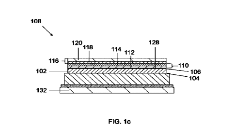
Figure la shows a liquid cooled ultrasonic transducer, in accordance with one
embodiment. Figure lb shows
a backing structure in contact with a piezoelectric material of the ultrasonic
transducer of Figure la. Figure
lc is a cross-section of Figure lb. Figure id is a cross-section of Figure la.
Figure 2 is an exploded view of a liquid cooled ultrasonic transducer, in
accordance with another
embodiment.
Figure 3 is another exploded view of the liquid cooled ultrasonic transducer
illustrated in Figure 2.
Figure 4 illustrates a backing structure in contact with a piezoelectric
material of the ultrasonic transducer,
and a heat sink in thermal contact with the backing structure, in accordance
with one embodiment
Figure 5 shows a single de-matching layer sandwiched between a piezoelectric
material and a dual layer de-
matching backing, in accordance with one embodiment.
Figure 6 is across-section of Figure 5.
Figure 7 illustrates a 16-element one-dimensional linear array, in accordance
with one embodiment.
Figure 8 is a cross-section of Figure 7, illustrating the layers forming the
16-element one-dimensional linear
array.
Figure 9 is another cross-section of Figure 7, illustrating the layers forming
the 16-element one-dimensional
linear array
Figure 10 illustrates a 16-element one-dimensional linear army, in accordance
with another embodiment.
CA 03158819 2022-5-18
WO 2021/097561
PCT/CA2020/051563
22
Figure 11 is a cross-section of Figure 10, illustrating the layers forming the
16-element one-dimensional
linear array.
Figure 12 is another cross-section of Figure 10, illustrating the layers
forming the 16-element one-
dimensional linear array
Figure 13 is a simplified illustration of the working principle of ultrasonic
transducer. More specifically,
considering a relatively narrowband case, them is shown the interaction of the
reflection coefficients and
the particular arrangement of low and high acoustic impedance layers in the
DLDBs resulting in only in-
phase reflections arriving at the output (front) face of the transducer. Due
to the resonance of each DLDB
layer, and the resulting phase of the alternating pairs, energy only leaves a
layer in phase every four
reflections and is partially destructively interfered with every two
reflections. The result is that the energy
once trapped in the DLDB layers takes a relatively long time to ring down, and
at very low amplitude.
Figure 14 shows a two-dimensional piezoelectric matrix, in accordance with one
embodiment.
Figure 15 is an exploded view of Figure 14_
Figure 16 is a cross-section of Figure 14.
Figure 17 shows an ultrasonic transducer, in accordance with another
embodiment.
Figure 18 shows an ultrasonic transducer, in accordance with another
embodiment.
Figure 19a is a comparison of state-of-the-art air-backed material specific
transducer (top) transmitting into
Titanium at 680 kHz with no heat sink and the ultrasonic transducer of Figure
la (bottom) at the same
conditions. Figure 1% is a comparison of log of the envelope of the state-of-
the-art air-backed material
specific transducer transmitting into titanium (top) and the ultrasonic
transducer of Figure la transmitting
into titanium(bottom).
Figure 20 is a comparison of three 680 lcHz material specific transducers
having copper heatsinks attached
to the back surface of the piezoelectric stack: air backed material specific
transducer with a heatsink directly
bonded to the back surface of the piezo electric element of the transducer
(top); state-of-the-art method of
bonding a heat sink to the piezo electric element of the transducer with
acoustically lossy thermally
conductive material such as alumina filled silicone foam (middle); and the
ultrasonic transducer of Figure
la, having a heatsink directly bonded to the backing structure (bottom).
Figure 21 shows the Log of the envelope of the waveforms shown in Figure 20.
CA 03158819 2022-5-18
WO 2021/097561
PCT/CA2020/051563
23
Figure 22a is a comparison of 10 MHz single element transducers, pulse echo
pulse response with a 'A
lambda resonant piezoelectric element and a ¨ 1/10th lambda thick tungsten de-
matching layer, illustrating
the effect of adding a single DLDB to the back of the de-matching layer.
Figure 22b shows the Log envelope
comparison of the waveforms of the 10 MHz single element transducers shown in
Figure 22a.
Figure 23a is a comparison of the effects of adding a 3 mm thick copper heat
sink directly to the back of the
MHz acoustic stacks from Figure 22a, the DML backing bonded directly to the 3
mm copper heatsink
develops multiple internal reflections which result in unwanted artifacts in
imaging or inspection
applications (top); and the DLDB equipped stack experiences no measurable
changes when the heat sink is
bonded directly to the surface of the acoustic stack (bottom). Figure 23b is a
comparison of the Log
10 envelopes of the pulse echo waveforms of the 10 transducer shown
in Figure 23a.
Figure 24 is a comparison of a pulse echo response from a material specific 5
MHz ID array element 550
urn by 5 ram with a PZT composite piezo element matched to transmit into
titanium with dual DLDB
backing compared to one with air backing. Minimal difference is seen between
the air backed transducer
(top) and the DLDB equipped transducer (bottom) apart from a minor pulse
length increase seen in the
DLDB equipped stack.
Figure 25 is a comparison of the pulse echo response of the transducer
elements described in Figure 24 with
the addition of a 6 mm copper heatsink directly bonded to the back of the
acoustic stacks (top). Significant
internal reverberation artifacts are seen when the heat sink is bonded to the
back of the air backed transducer
(bottom).
DETAILED DESCRIPTION
In the following description, similar features in the drawings have been given
similar reference numerals,
and, to not unduly encumber the figures, some elements may not be indicated on
some figures if they were
already identified in one or mom preceding figures. It should also be
understood herein that the elements of
the drawings are not necessarily depicted to scale, since emphasis is placed
upon clearly illustrating the
elements and stnictures of the present embodiments. The terms "a", "an" and
"one" are defined herein to
mean "at least one", that is, these terms do not exclude a plural number of
elements, unless stated otherwise.
It should also be noted that terms such as "substantially", "generally" and
"about", that modify a value,
condition or characteristic of a feature of an exemplary embodiment, should be
understood to mean that the
value, condition or characteristic is defined within tolerances that are
acceptable for the proper operation of
this exemplary embodiment for its intended application.
CA 03158819 2022-5-18
WO 2021/097561
PCT/CA2020/051563
24
In the present description, the terms "connected", "coupled", and variants and
derivatives thereof, refer to
any connection or coupling, either direct or indirect, between two or more
elements. The connection or
coupling between the elements may be acoustical, mechanical, physical,
optical, operational, electrical,
wireless, or a combination thereof.
It will be appreciated that positional descriptors indicating the position or
orientation of one element with
respect to another element are used herein for ease and clarity of description
and should, unless otherwise
indicated, be taken in the context of the figures and should not be considered
limiting_ It will be understood
that spatially relative terms (e.g., "outer" and "inner", "outside" and
"inside", "periphery" and "central",
"over" and "under", and "top" and 'bottom") are intended to encompass
different positions and orientations
in use or operation of the present embodiments, in addition to the positions
and orientations exemplified in
the figures.
General theoretical context
A piezoelectric ultrasound transducer is generally composed of a piezoelectric
element having two opposing
faces. The piezoelectric element can be chosen to operate at a desired
frequency. An example of such an
operation includes the acoustics resonance of the piezoelectric element
Piezoelectric acoustic transducers
can include a plurality of layers, which can be, for example and without being
limitative, stacked or overlaid.
In addition to the piezoelectric element(s), a piezoelectric acoustic
transducer can include at least one of:
signal and ground electrode(s), matching layer(s), acoustic backing(s),
lens(es) and many other layer(s) or
structure(s) to improve their performance in their intended application. Some
transducers can be designed
to output acoustic energy (i.e, transmitters), while others can detect
impinging acoustic energy (i.e.,
receivers). It is to be noted that some transducers can be optimized to
perfonn both functions (i.e.,
transceivers). Different techniques may be implemented in the field of
ultrasonic transducers to produce
different types of piezoelectric ultrasonic transducers,
In most cases, designing a piezoelectric transducer is associated with
numerous challenges, for instance the
optimization andfor the direction of acoustic energy to the intended target,
as well as the minimization of
the acoustic energy away firom the intended target. For example, one may
consider the relatively simple case
of a thin disc shaped piezoelectric element, which when an appropriate
frequency voltage is applied across
the piezoelectric disc, will tend to produce equal acoustic waves from both
the front and back faces of the
disc.
There exists a broad variety of techniques to refine the characteristics of
such a piezoelectric disc to enhance
the acoustic energy output from one face (the front face or distal face, for
example), and diminish it from
the other face (the back face, or proximal face). One skilled in the art will
know that such a piezoelectric
CA 03158819 2022-5-18
WO 2021/097561
PCT/CA2020/051563
element is generally placed such that each face is in contact with an
electrically conductive electrode. An
example of electrically conductive electrode is sputtered metal, which allows
the piezoelectric element to
be connected to electronic systems and/or other appropriate circuits. In the
implementations wherein an RF
voltage signal is applied to the electrodes, the piezoelectric element
undergoes a mechanical perturbation.
5 If the frequency of the electric RF signal and the thickness of the one-
dimensional piezoelectric array match
correct operation conditions, then the piezoelectric element may be made to be
mechanically resonant at
ultrasonic frequencies One would note that such a possibility depends on the
characteristics of the
piezoelectric material.
It is generally known in the art that backings can be used in piezoelectric
ultrasonic transducers. Examples
10 of backing includes, but are not limited to absorbing backings having
acoustic impedance much lower than
the piezoelectric layer, some having composite forms to dissipate and absorb
acoustic energy, de-matching
layers having acoustic impedance much higher than the piezoelectric layer and
thickness typically less than
'A lambda designed to efficiently reflect all energy to the output of the
transducer while allowing a tunable
mass loading effect, as well as other technologies such as air backing, and
many other variations including
15 delay line backings and still others.
Many transducer backings are low acoustic impedance absorbing backings and are
designed to reflect the
majority of or at least a significant portion of the energy toward the front
(or, alternatively the "working
face") of the transducer and absorb and dissipate the un-reflected energy
within the backing. Such absorbing
backings generally have a predetermined geometrical configuration, for
instance the backings can be
20 sufficiently large and have a specific shape to absorb enough acoustic
energy and prevent unwanted internal
reflections from returning to the piezoelectric crystal. These low acoustic
impedance backings typically
require that the piezoelectric layer operate in 'A lambda resonant mode_
De-matching layers are another common backing technology, designed to reflect
the energy out the front of
the transducer, while providing a somewhat adjustable mass load for tuning
damping. The effect of adding
25 a de-matching layer generally requires the design of a 1/4 wave resonant
transducer. In some
implementations, the de-matching layers can be operated to reflect close to
100 percent of the energy, or at
least a significant portion of the energy.
Another implementation includes air backed transducers, which can also reflect
close to 100 percent of
energy out the front, or at least a signification portion thereof. However,
such transducers do not allow for
mass loading or damping but will work in the same mode as a light absorbing
backing, in that the
piezoelectric will resonate at 1/2 lambda.
CA 03158819 2022-5-18
WO 2021/097561
PCT/CA2020/051563
26
One limitation of most backing technologies, amongst others, is that the back
of the transducer is not
accessible for electrical connection without compromising the acoustic signal
and should generally be made
off to the side of in a minimal footprint to minimize acoustic artifacts
and/losses. A further limitation of
existing technologies is the difficulty in providing for efficient thermal
cooling solutions in direct contact
with the piezoelectric elements of the transducer. The aforementioned
challenges are of increasing
significance as modem relaxor-based polycrystalline and single crystal
ferroelectrics become more and
more efficient at the expense of thermal robustness_
It is to be noted that 2-D array transducers can make both cooling and
electrical interconnection and acoustic
backing considerations more challenging due to the lack of access to the
interior elements of a matrix
transducer. As a result, there exists a need to develop an acoustically
efficient backing that is electrically
conductive, as it will be herein described. There is also a need to develop an
acoustically efficient backing
technology that is thermally conductive, as it will be herein described. There
is also a need to develop an
acoustically and spatially efficient backing that is capable of reflecting
nearly all of the acoustic energy of
the piezoelectric transducer while leaving the proximal face of the backing
relatively free of acoustic energy
making the connection of electrical and or thermal devices possible without
disrupting the performance of
the transducer, as it will be herein described. There exists a need to develop
a thermally conductive and
electrically conductive acoustically efficient backing that can be connected
to a l-D or 2-D array transducer
providing electrical connectivity to each element, cooling to each element, as
it will be herein described.
Backing structuresfor ultrasonic transducers
Broadly described, the present description relates to multilayered ultrasound
transducer backing structures
or similar technologies. In some embodiments, the technology allows reflecting
a significant portion and,
in some instances, virtually all acoustic energy out the front of the
transducer. Additionally, the systems or
devices made according to the current technology are generally not affected by
physical contact at the back
of the backing stack. The transducers that will be herein presented are
thermally electrically and acoustically
relatively efficient as very little energy is absorbed in backing layers.
In the context of the current disclosure, and as it will be described in
greater detail below, the backing
structure may include one or more de-matching backings, each including two
layers. In this regard, each de-
matching backing will be referred to as a "dual layer de-matching backing", or
simply "DLDB". In some
embodiments, a DLDB pair can be used as the backing structure, i.e., the
ultrasonic transducer may include
a first DLDB and a second DLDB, each DLDB including two layers. In other
embodiments, two or more
of DLDB pairs can be used as the backing structure, for example and without
being limitative, to ftuther
acoustically isolate the back surface.
CA 03158819 2022-5-18
WO 2021/097561
PCT/CA2020/051563
27
Of note, the layers forming the DLDB have electrical, acoustical, thermal and
mechanical properties, and
these properties may vary according to the targeted application. For example,
and without being 'imitative,
the DLDB may include layers that are electrically conductive and thermally
conductive, layers that are
neither electrically or thermally conductive, or any combinations thereof.
With reference to Figures 1 to 6, embodiments of an ultrasonic transducer 100
will be described.
The ultrasonic transducer 100 generally includes a piezoelectric material 102,
a backing structure 108, a
heat sink 122, and one or more electrodes 126 (referred to as the electrodes
126). While the embodiments
of the ultrasonic transducer that will be described throughout the description
will be described as including
a piezoelectric material, one skilled in the art would note that the
ultrasonic transducers of the current
disclosure may instead include any ferroelectric materials, any single
crystals or polycrystalline materials,
any electromechanical transduction materials, such materials having one or
more of the following
properties: ferroelectricity, pyroelectricity, piezoelectricity,
electrostriction and/other relevant properties. It
will be noted that, in the context of the present description, the expression
"piezoelectric material" may also
refer to ferroelectric material, pyroelectric material, relaxor material and
electrostrictive material, as it would
be readily understood by one skilled in the art.
The piezoelectric material 102 has a front surface 104 and a back surface 106.
The piezoelectric material
102 is configured to be in acoustic communication with a sample (not
illustrated in the Figures). The
piezoelectric material 102 has acoustic properties. For example, and without
being [imitative, the acoustic
properties may include an acoustic impedance of about 275 MegaRayls.
In some embodiments, the piezoelectric material 102 may be a poled composite
piezoelectric disc. The
poled composite piezoelectric disc may be in a 1 3 configuration.
In some embodiments, the piezoelectric material 102 may be a composite of PZT4
and may include pillars.
For example, and without being limitative, the pillars may be 1000 um by 1000
urn pillars separated by 200
urn kerfs. The kerfs may be cut at a pitch of about 1200 tint The kerfs may be
filled with a composite filler.
In some embodiments, the composite filler may be in a 0 3 configuration. The
composite filler may include
particles of hafnium dioxide doped into epoxy. A nonlimitative example of
epoxy is Epo-Tek 301. In
some embodiments, the piezoelectric material 102 may have a thickness included
in a range extending from
about 2.35 min to about 2.45 min
In some embodiments, the piezoelectric material 102 consists of a
piezoelectric layer_
The backing structure 108 is positioned at the back surface 106 of the
piezoelectric material 102. The
backing structure 108 is configured to reflect acoustic energy towards the
front surface 104 of the
piezoelectric material 102. In some embodiments, the backing structure 108 is
further configured to reflect
CA 03158819 2022-5-18
WO 2021/097561
PCT/CA2020/051563
28
the acoustic energy in phase. In some embodiments, the backing structure 108
is further configured to
spatially and temporally disperse unwanted acoustic reverberations in the
backing structure 108. The
backing structure 108 is thermally conductive and electrically conductive. The
backing structure 108
illustrated in Figures 1 to 6 includes a first dual layer de-matching backing
110 and second dual layer de-
matching backing 116.
The first dual layer de-matching backing 110 includes a first layer of
graphite 112 and a layer made of
tungsten 114 in contact with the first layer of graphite 112. In some
embodiments, the first layer of graphite
112 has an acoustic impedance of about 5.1 MegaRayls and has a thickness
included in a range extending
from about 1.5 mm to about 1.6 mm. In some embodiments, the layer of tungsten
114 has an acoustic
impedance of about 100 MegaRayls and a thickness included in a range extending
from about 2.6 mm to
about 2.7 mm. One skilled in the an would readily understand that the acoustic
impedance and the thickness
of the first layer of graphite 112 and the layer of tungsten 114 are dictated
by the targeted application, and
so could be different from the examples listed above.
The second dual layer de-matching backing 116 contacts the first dual layer de-
matching backing 110. The
second dual layer de-matching backing 116 includes a second layer of graphite
118 and a layer of copper
120 in contact with the second layer of graphite 118. In some embodiments, the
second layer of graphite
118 has an acoustic impedance of about 5.1 MegaRayls and a thickness included
in a range extending from
about 1.5 nun to about 1.6 mm. In some embodiments, the layer of copper 120
has an acoustic impedance
of about 41.5 MegaRayls and has a thickness included in a range extending from
about 2.5 mm to about 2.6
mm. One skilled in the art would readily understand that the acoustic
impedance and the thickness of the
second layer of graphite 118 and the layer of copper 120 are dictated by the
targeted application, and so
could be different from the examples listed above.
The heat sink 122 is in thermal contact with the backing structure 108. In
some embodiments, the heat sink
122 includes at least one channel 124. Such a channel 124 is configured for
receiving and circulating a heat
transfer fluid therein. The heat transfer fluid may be a liquid, gaseous, or
any mixtures thereof. In some
embodiments, the heat sink 122 is electrically insulated from the backing
structure 108
The electrodes 126 are in electrical communication with the piezoelectric
material 102. In some
embodiments, the ultrasonic transducer 100 includes a control unit (not
illustrated in the Figures) electrically
connected to at least one of the piezoelectric material 102, the backing
structure 108 and the electrodes 126.
Such a control unit may be useful to control the ultrasonic transducer 100. In
some embodiments, the
electrodes 126 are electrically connected to the piezoelectric material 102
through the backing structure 108.
The ultrasonic transducer 100 is operable at an operational frequency. This
operational frequency is related
to an operational wavelength 1.o. In some embodiments, the first layer of
graphite 112, the layer made of
CA 03158819 2022-5-18
WO 2021/097561
PCT/CA2020/051563
29
tungsten 114 in contact with the first layer of graphite 112, the second layer
of graphite 118 and the layer
of copper 120 each have a corresponding thickness of about ko14 thick or odd
multiples of ha/4. In some
embodiments, the operational wavelength lo may be about 530 kHz.
hi one embodiment, the piezoelectric material 102 is configured to be half
wave resonant at the operational
frequency.
In another embodiment, the ultrasonic transducer 100 includes a single de-
matching layer 128 positioned
between the piezoelectric material 102 and the backing structure 108. The
single de-matching layer 128 is
in acoustic communication with the piezoelectric material 102 and the backing
structure 108. The single de-
matching layer 128 has a corresponding acoustic impedance relatively higher
than an acoustic impedance
of the piezoelectric material 102. In this embodiment, the piezoelectric
material 102 is configured to be
quarter wave resonant at the operational frequency. The piezoelectric material
102 has a resonant frequency,
and this resonant frequency is related to a resonant wavelength kr. The single
de-matching layer 128 has a
thickness of less than Dur/5 thick with respect to the resonant frequency of
the piezoelectric material 102.
The single de-matching layer 128 may have a thickness ranging between about
1.r/10 and about 1,r/20. The
single de-matching layer 128 may be made, for example and without being
limitative, from tungsten. Other
materials could be used for the single de-matching layer 128. In some
embodiments, the resonant
wavelength Is may be about 530 kHz.
In some embodiments, the ultrasonic transducer includes a thermally conductive
structure 130 in contact
with the backing structure 108. In some embodiments, the thermally conductive
structure 130 is electrically
insulated from the backing structure 108. In some embodiments, the thermally
conductive structure 130 may
be a layer made of AIN or a layer made of beryllium oxide. In some
embodiments, the thermally conductive
structure 130 may extend on lateral portions of the backing structure 108. In
some embodiments, the
thermally conductive structure 130 includes at least one electrically
conductive via passing through the
thermally conductive structure 130.
hi some embodiments, the ultrasonic transducer 100 includes a wear layer 132
having abrasion-resistant
properties. The wear layer 132 may be made, for example and without being
[imitative, from titanium.
ht some embodiments, the ultrasonic transducer 100 includes a thermally
conductive layer 133 acoustically
matched with the piezoelectric material 102. As depicted in Figure ld, the
thermally conductive layer 133
may be provided between the piezoelectric material 102 and the wear layer 132.
Such a thermally conductive
layer may be in thermal contact with the heat sink 122 through a copper lid
135. Of note, the lid 135 could
be made from any other thermally conductive material.
In some embodiments, the ultrasonic transducer 100 has a diameter of about 50
mm.
CA 03158819 2022-5-18
WO 2021/097561
PCT/CA2020/051563
Examples
Other embodiments of The ultrasonic transducer having been insofar described
will now be presented.
In some embodiments, the ultrasonic transducer includes two stacked DLDBs
stacked (Dual DLDB stack)
on a single element liquid cooled material specific transducer designed to
match titanium_ One exemplary
5 embodiment of the DLDB designed to operate on a 680 kHz piezoelectric
transducer having a
piezocomposite element of 27.5 MegaRayls (MR) acoustic impedance includes a
first DLDB bonded to a
second DLDB pair, the first DLDB pair includes a first layer of graphite
having an acoustic impedance of
approximately 5.1 MR and a thickness of 1.03 mm, and a second layer of
tungsten metal having an acoustic
impedance of approximately 100 MR and a thickness of 1.53mm ,the second DLDB
pair includes of a first
10 layer of graphite having an acoustic impedance of approximately
5.1 (MR) and a thickness of 0.905 mm,
and a second layer of copper metal having an acoustic impedance of
approximately 41.5 MR and a thickness
of 1.71 mm.
In some embodiments, one or two DLDBs on a single element transducer having a
high acoustic impedance
de-matching layer (DML) of less than 2/5 lambda and typically less than 1/4
lambda, interposed between
15 the DLDB stacks and the piezo element.
In some embodiments, the DLDB includes a first backing layer and a second
backing layer, each having a
distal face and a proximal face. The proximal face of the first backing layer
can be in acoustic contact with
the distal thee of the second backing layer; the two layers together
comprising the DLDB structure. The
DLDB, in turn, can be placed in acoustic contact with a piezoelectric element
having a distal and a proximal
20 face, the distal face of the first backing layer being in
contact with the proximal face of the piezoelectric
element. The first and second backing layers of the DLDB can be designed to be
about 'A lambda thickness
for the designed resonant frequency of the piezoelectric element. The first
backing layer can be made from
a material having a relatively lower acoustic impedance as compared to the
piezoelectric element. The
second backing layer can be made from a material having a relatively higher
acoustic impedance compared
25 to the first backing layer.
In the embodiments wherein two or more DLDBs are stacked, an improved or
increased acoustic isolation
from electrical and thermal structures connected to the transducer through the
DLDB may be achieved.
In some embodiments, in operation, the first face of the first layer of the
first DLDB reflects the majority of
the acoustic energy directed towards the backing of the transducer back out
the working face of the
30 transducer, while the back face of the first layer also
reflects most of the energy that reaches it, doing so in
phase. The layers of the DLDB then begin to resonate with the remaining energy
in the backing, over the
bandwidth of the transducer due to Vi wave layers and alternating sign of the
reflection coefficients due to
CA 03158819 2022-5-18
WO 2021/097561
PCT/CA2020/051563
31
the transition from low to high acoustic impedance in the layers included in
the DLDB. The resonating
layers then release the energy in phase both forward and backwards through the
backing stack, over a
relatively long period of time and at a very low amplitude, effectively
spreading unwanted reflections out
over time at an acceptably low amplitude.
The embodiments of the DLDB having been described may be effective on acoustic
stacks having been
designed for Vz lambda resonant piezoelectric transducers and an intended load
that is greater than the
acoustic impedance of the light layer of the DLDB(s) and well matched to the
acoustic impedance of the
piezoelectric layer. Example of such structures can be found in PCT patent
application
PCT/CA2019/051046, the content of which is herein incorporated by reference.
The embodiments of the DLDB as described herein can also be effective on
acoustic stacks having been
designed for V2 lambda resonant piezoelectric transducers and an intended load
that is greater than the
acoustic impedance of the light layer of the DLDB. When the load is comparable
to or lower than the lower
acoustic impedance layer of the first DLDB layer, the transducer can include a
piezoelectric layer having
higher acoustic impedance than the load and one or more matching layers.
In some embodiments, the DLDB can be used with a 1/4 lambda stack in
conjunction with a de-matching
layer. In another example, the DLDB can be included with a high acoustic
impedance de-matching layer
into a lambda resonant piezoelectric transducer design, wherein the high
acoustic impedance de-matching
layer is interposed between the DLDB and the piezoelectric material with
nearly no restriction to the
acoustic impedance of the load material. This technique may be applied to
material specific transducers, or
transducers having matching layers or any other practical load matching
method.
A variation of the thickness of the DLDB layers can be used to expand the
bandwidth of the transducer and
to improve the reflectivity of the backing over a broader frequency spectrum.
Such a variation can be
implemented depending on the targeted application.
Due to the relatively high acoustic isolation achieved by the DLDB and the
possibility of making the layers
thermally conductive, it is possible to directly apply a heat sink to the
proximal face of the DLDB, resulting
in a highly efficient removal of heat directly from the back of the
piezoelectric element without
compromising the acoustic properties of the transducer.
Due to the relatively high acoustic isolation achieved by the DLDB and the
possibility of making the layers
electrically conductive, it is possible to make electrical connection directly
to the proximal face of the DLDB
by, for example, soldering, wire bonding, or using conductive epoxy to attach
a wire or other electrical
circuit to the top layer of the DLDB.
CA 03158819 2022-5-18
WO 2021/097561
PCT/CA2020/051563
32
In some embodiments, it is further possible to dice the DLDB into elements
aligned with the piezoelectric
elements of a transducer array such as, for example, a 1-D linear army, a 2-D
matrix army, or other multi
element transducer arrays such that one can apply a printed circuit board, or
ASIC interposer, electrical
connector, or other electrical circuit directly to the proximal face of the
DLDB, making a highly efficient
electrical connection to the transducer. This can be useful when the
ultrasonic probe is a 2-D multi-element
array making the connection to a relatively large number of elements possible
in directly to the DLDB
corresponding to each element of the array without compromising the acoustic
properties of the transducers_
These embodiments will be described in other sections of the description.
Due to the backing being relatively low profile and enabling direct electrical
connection to the low profile
DLDB, the present technology can provide advantages in terms of design when it
comes to low-profile
ultrasonic probes. Examples of low-profile ultrasonic probes include but are
not limited to probes used for
intracavity medical probes, endoscopes, and NDT cylindrical transducers and
arrays.
In some embodiments, the DLDB has one or more layers, each being made from a
thermally conductive
material that is laterally electrically insulating and axially conductive,
thus resulting in an isotropic
thermally conductive and anisotropic electrically conductive layer. In one
embodiment, the high acoustic
impedance layer is made from an aluminum nitride (AIN) ceramic for example.
The high acoustic
impedance layer has a plurality of electrically conductive vias arranged to
align with a multi-element array
element. The other layer of the DLDB can be separated into laterally
electrically and acoustically isolated
elements, aligned with the elements of the piezoelectric array by, for
example, dicing, etching, or machining
or by other methods. The combination of these two layers results in a backing
that provides electrical
connectivity from each transducer element to the proximal surface of the DLDB,
lateral electrical isolation
from one element to every other element though the entire DLDB and
piezoelectric stack, and contiguous
and/or continuous lateral thermal conductivity over the entire array of
elements. One skilled in the art will
understand that heat sinking of the transducer can then be achieved by
removing heat from the perimeter of
the AIN layer through the use of some means of cooling technology, for
example, an air-to-air heat
exchanger, or for example a liquid cooling heat sink, while still enabling
direct electrical connection of the
array to a PCB or interposer. It can be readily seen by one skilled in the art
that this approach can be adapted
to multiple DLDB stacked to increase acoustic isolation and/or thermal
conductivity. This use of electrically
isolated thermally contiguous and/or continuous DLDBs in 1-D and especially 2-
D transducer array allows
direct cooling of large arrays without compromising acoustic performance and
affording a relatively simple
and cost-effective means of electrical interconnection.
In some embodiments, the DLDB may be liquid cooled.
CA 03158819 2022-5-18
WO 2021/097561
PCT/CA2020/051563
33
In some embodiments, there is provided a liquid cooled DLDB equipped 680 kHz
material specific
transducer for use with titanium and other similar acoustic impedance
materials (such as zirconium). The
transducer may have a 50 mm diameter and a dual DLDB equipped stack.
One would note that the transducer is an exemplary embodiment of the
technology and serves an illustrative
purpose only. Apart from what is being disclosed in the current description,
the transducer could include
some other elements known one skilled in the art.
In some embodiments, the transducer comprises a 2.4 mm thick 1 3 poled
composite piezoelectric disc, the
thickness corresponding to about between 0.35 and 0.4 lambda in an unloaded
free resonance condition, but
operating in 'A lambda mode, having a positive electrode on the proximal face
and negative electrode on the
distal face. As one skilled in the art will understand, the thickness of the
piezoelectric disc is chosen to be
thinner than 1/2 lambda to compensate for the mass loading effect of the DLDB
backing and acoustic loads.
The piezoelectric composite can be made by dicing and filling poled PZT4
material having 200 urn kerfs
cut at a pitch of 1200 um leaving 1000 urn by 1000 urn pillars separated by
200 urn kerfs. The kerfs can be,
for example and without being limitative, filled with a 0 3 composite filler
of c.a. 5 um particles of hafnium
dioxide doped into Epotek 301 epoxy, such that the acoustic impedance of the
composite kerf filler
material ranges between approximately 7 to 8 Mega Ray's (MR), and the acoustic
impedance of the overall
piezocomposite layer is closely matched to titanium being approximately 27.5
MR. The negative face of the
piezoelectric composite layer can be bonded to the proximal face of a 6 mm
thick disc of ZA-8 zinc-
aluminum alloy, using, for example, a tungsten powder loaded epoxy. The distal
face of the ZA-8 disc, can
then be bonded to the proximal face of an alumina composite disc, using a
submicron particle hafnium oxide
loaded Epotek 301 epoxy. The alumina composite disc can include pillars of 750
um by 750 urn by 1400
urn height, separated by kerfs of 200 urn, the kerfs being filled with the
same hafnium particle loaded epoxy
used to make the piezoelectric composite disc. The distal face of the alumina
composite can be bonded in
turn to the proximal face of a 3 mm thick disc of titanium, with a layer of
submicron hafnium oxide loaded
Epotek 301 epoxy. Two sets of dual layer de-matching backings (DLDB) are then
bonded to the proximal
face of the piezoelectric disc using sub-micron tungsten powder loaded epotek
301 epoxy as follows. The
proximal face of the piezoelectric composite disc is bonded to the distal face
of a 1030 urn thick Paco DFP-
1 graphite disc, having acoustic impedance of 5.1 MR, 905 urn corresponding to
'A lambda at 680 kHz, the
centre frequency of the transducer. The proximal face of the graphite disc is
then bonded to the distal face
of a 1530 urn thick tungsten disc, having acoustic impedance of 100 MR, the
thickness of the tungsten disc
corresponding to 'A lambda at ¨ 850 kHz, also slightly above the center
frequency of the transducer. The
proximal face of the tungsten disc is then bonded to the proximal face of a
905 um thick Poco DFP-1 graphite
disc, having acoustic impedance of 5.1 MR., the thickness corresponding to 'A
lambda at ¨800 kHz, slightly
above the centre frequency of the transducer. The proximal face of the
graphite disc is bonded to the distal
CA 03158819 2022-5-18
WO 2021/097561
PCT/CA2020/051563
34
face of a 1710 urn thick copper disc, having acoustic impedance of 41.5 MR,
the thickness corresponding
to 'A lambda at 680 kHz. The graphite disc, and tungsten disc, constitute the
first dual-layer de-matching
backing stack, and the graphite disc and copper disc constitute the second
DLDB stack. These two stacks
work together to acoustically isolate the piezoelectric composite disc from
the thermal cooling elements of
the transducer, allowing the thermal cooling solution to be directly bonded to
the proximal face of the copper
disc without substantially disrupting the acoustic performance of the
transducer. In these embodiments, the
distal face of a 1 mm thick highly thermally conductive AIN disc is bonded to
the proximal face of the
copper disc, using thermally conductive epoxy. The MN disc is notched to allow
space for electrical
connection to the copper disc to be made with a soldered wire, or
alternatively, a conductive epoxy bonded
wire. It should be noted that the entire DLDB stack in this embodiment is both
electrically and thermally
conductive, making electrical connection to the signal electrode of the
piezoelectric composite disc possible
directly through the DLDB stacks. In addition, it should be noted that many
materials exist that can be
practically used in the application of the disclosed technology beyond those
being explicitly described in
this exemplary embodiment, some of which arc electrically conductive,
thermally conductive, or both, or
neither thermally or electrically conductive. In this exemplary embodiment,
the DLDB layers are all both
electrically and thermally conductive. The proximal face of a copper heat sink
base is brazed or soldered to
the distal edge a heat-sink top, to form a hollow copper heat sink assembly,
the distal face of which is
directly bonded to the proximal face of the MN disc, with themtally conductive
but electrically insulating
epoxy. In the illustrated embodiments, the proximal face of the hollow heat
sink top is bonded with the same
thermally conductive epoxy to the distal face of an AIN disc. The AIN disc has
two clearance holes in it and
a notch, the holes allowing for the cooling tubes, to be affixed to the
integral barbed tubes of the heat sink
top, and the notch allowing a clearance path for the signal wire attached to
the copper DLDB layer. The
proximal face of the MN disc can be bonded to the distal face of the copper
heat spreader using thermally
conductive epoxy. The copper housing shell can be press fit onto the perimeter
of ZA-8 disc and bonded to
the complete acoustic and theme' stack using an electrically insulating and
thermally conductive epoxy. In
some embodiments, all the voids are filled with thermally conductive
electrically insulating epoxy, thus
making the entire assembly solid, apart from the hollow interior of the
heatsink assembly (i.e., heatsink top
and heat sink bottom). Rubber hoses, which can have, for example and without
being limitative, an inner
diameter of 3/8 of an inch, are fitted to the top copper heatsink barbed hose
bosses and fixed in place with
hose clamps. The transducer includes an electrical contact, which can be
embodied by a BNC RF electrical
connector, soldered to the copper lid. The centre conductor of the BNC
connector can further be soldered
to the signal wire thus electrically connecting the BNC signal conductor to
the positive signal electrode of
the piezoelectric composite disc. The copper lid can, in some embodiments, be
soldered or bonded with
conductive epoxy to the proximal lip of the copper shell, completing the
electrical connection from the
ground of the HNC connector and the negative electrode of the piezoelectric
composite disc via the copper
CA 03158819 2022-5-18
WO 2021/097561
PCT/CA2020/051563
shell and the ZA-8 disc. The transducer also includes an electrically
insulating plastic housing, bonded to
the copper lid and copper shell, at least partially covering the edge of the
alumina composite disc and resting
on the surface of titanium disc. The resulting transducer (Le., the assembly
of the components which have
been previously described) is then connected to a liquid circulating air-to-
liquid heat exchanger and filled
5 with a suitable cooling liquid. A nonlimitative example of cooling liquid
is a 50% propylene glycol/water
mixture.
These embodiments can be used to provide direct cooling to the signal
electrode of the piezoelectric
composite disc, via the dual DLDB stacks, as well as indirect cooling to the
ground electrode of the
piezocomposite disc, via the copper shell and ZA-8 disc, allowing for the
removal of hundreds of Watts
10 with coolant flow rates of about a few liters per minute and a heat
exchanger. More specifically, in some
embodiments, the ultrasonic transducer may include a thermally conductive
layer acoustically matched with
the piezoelectric material to allow such an indirect cooling. Additionally,
the design being herein described
allows for high bandwidth of over 90% one way (e.g., 6 dB bandwidth for the
exemplary transducer), and
negligible reverberation artifacts to be possible while directly cooling the
piezoelectric element with an
15 efficient liquid filled metal heat sink.
In some embodiments, there is provided a stack of piezoelectric layer and DLDB
for liquid cooled
transducers. Five layers may be superimposed, but it would be readily
understood that that they could
coextend along an entirety or only a portion of their surface. The layer is a
single element 'A lambda
piezoelectric composite layer matched to titanium. The layer is a low acoustic
impedance Vi lambda graphite
20 layer of the first DLDB stack. The layer is a high acoustic impedance
lambda tungsten layer of first DLDB
stack. The layer is a low acoustic impedance i/4 lambda graphite layer of
second DLDB stack, The layer is
a high acoustic impedance './4 lambda copper layer of first DLDB stack_
In some embodiments, the ultrasonic transducer includes a titanium wear layer,
an aluminum oxide (AIN)
composite electrical isolation layer, and a thermally, electrically, and
acoustically conductive layer. The
25 layer can be, for example and without being limitative, made of zinc or
zinc alloy, and be acoustically
matched to titanium while being a better themial conductor. The transducer
further includes a single element
'/2 lambda piezoelectric composite layer. The layer can be matched to
titanium. The transducer includes a
first and second DLDB stacks, each including a low acoustic impedance layer
and a high acoustic impedance
layer. More particularly, the first DLDB stack includes a low acoustic
impedance 'A lambda graphite layer
30 and a high acoustic impedance 'A lambda tungsten layer, and the second
DLDB stack includes a low acoustic
impedance E/4 lambda graphite layer and a high acoustic impedance 1/4 lambda
copper layer. The transducer
according to this embodiment further includes a thermally conductive
electrical insulation layer. The layer
can be made of, for example and without being 'imitative, aluminum nitride.
The transducer also includes
CA 03158819 2022-5-18
WO 2021/097561
PCT/CA2020/051563
36
an electrically and thermally conductive housing, as well as an electrically
insulating plastic external
housing. Other components of the transducers include, but are not necessarily
limited to an electrically
insulating disc with hose cutouts, which can be made from AN, a water block
heat exchanger base, a water
block heat exchanger top, a heat transfer layer with hose cutouts, which can
be made from copper, a copper
housing lid, a BNC RF electrical connector and liquid cooling hoses.
In some embodiments, there is provided an acoustic Stack with two DLDB stacks
in place with a hilly
electrically isolated liquid cooling heat exchanger in direct thermal contact
with the copper layer of the
DLDB via an AIN electrical insulating layer
In some embodiments, there is provided a 10 MHz piezoelectric single element
traducer stack having a 0.12
lambda (62.5 urn) thick tungsten de-matching layer interposed between a dual
layer de-matching backing
stack includes of a 'A lambda thick (70 urn) low impedance graphite layer and
a 'A lambda thick (130 um)
high impedance tungsten layer. This includes a 10 MHz piezoelectric stack
having a 115 um thick 1 3 PZT
composite stack, a 62.5 um thick tungsten de-matching layer and a dual layer
de-matching backing stack.
The transducer according to this embodiment includes a single element 'A
lambda piezoelectric composite
layer, which can be matched to titanium. The transducer also includes a 0.12
lambda de-matching layer,
which can be made from tungsten. The transducer also includes one DLDB stack,
which includes a low
acoustic impedance 'A lambda layer which can be made of graphite and a high
acoustic impedance 1/4 lambda
layer which can be made of tungsten.
In some embodiments, there is provided 10 MB/ piezocomposite transducer
design. The acoustic stack may
include a piezoelectric composite disc, a tungsten de-matching layer, and a
dual de-matching backing stack
includes a graphite layer, and a tungsten layer. The piezo composite disc, has
acoustic impedance of
approximately 25 MR, thickness of 115 um, corresponding to approximately 1/4
lambda, and has a positive
pole and electrode on the proximal face, and negative pole and electrode on
the distal face of the disc. The
tungsten de-matching layer, is 62.5 um thick, corresponding to approximately
0.12 lambda. The graphite
layer, of the DLDB is 70 urn thick, corresponding to 1/4 lambda at 10 MHz, and
the tungsten layer, is 130
urn thick, also corresponding to 'A lambda at 10 MI-12. The acoustic stack is
bonded together using a low
viscosity epoxy, such as Cotronics 4461. Electrical connection is made by
loading a fraction of submicron
tungsten powder into the epoxy where required. One skilled in the art will
understand that for the purposes
of matching the pieze composite element to water 'A wave matching layers may
be used. For the purposes
of this exemplary embodiment, two 1/4 wave matching layers are used, the first
matching layer bonded to
the distal face of the pie zo composite layer, having acoustic impedance of
¨10 MR, and the second having
acoustic impedance of 3 MR. The results of simulated testing of this stack
with and without a copper heat
CA 03158819 2022-5-18
WO 2021/097561
PCT/CA2020/051563
37
sink bonded to the proximal face of the high acoustic impedance layer of the
DLDB, are shown in figures
22a, 22b, 23a, and 23b.
Different embodiments of an ultrasonic transducer including a one-dimensional
piezoelectric array will now
be described.
Ultrasonic transducers including a one-dimensional piezoelectric array
Now turning to Figures 7 to 12, there is illustrated an ultrasonic transducer
array 200.
The ultrasonic transducer array 200 includes a one-dimensional piezoelectric
array 202 having a front
surface 204 and a back surface 206. The one-dimensional piezoelectric array
202 is configured to be in
acoustic communication with a sample (not illustrated in the Figures). As
illustrated, the array 202 includes
a plurality of piezoelectric regions 203 arrayed in one dimension.
The ultrasonic transducer array 200 also includes a backing structure 208
positioned at the back surface 206
of the one-dimensional piezoelectric array 202. The backing structure 208 is
configured to reflect acoustic
energy towards the front surface 204 of the one-dimensional piezoelectric
array 201 In some embodiments,
the backing structure 208 is further configured to reflect the acoustic energy
in phase. In some embodiments,
the backing structure 208 is fiirther configured to spatially and temporally
disperse unwanted acoustic
reverberations in the backing structure 208. The backing structure 208
includes a dual layer de-matching
backing 210. In some embodiments, the backing structure 208 is thermally
conductive and electrically
conductive. In some embodiments, a top portion 209 of the backing structure
208 is made from an
electrically insulating material. In some embodiments, the top portion 209 of
the backing structure 208
includes a layer made from MN traversed by electrically conductive vias 236,
each electrically conductive
via 236 being aligned to a corresponding one of the plurality of piezoelectric
regions 203 arrayed in one
dimension. In some embodiments, the layer made from AIN layer has a front
face, and the layer made from
AIN layer is partially diced from the front face to enhance acoustic
separation of adjacent ones of the
plurality of piezoelectric regions 203 arrayed in one dimension.
The dual layer de-matching backing 210 includes a low acoustic impedance layer
212 and a high acoustic
impedance layer 214. In some embodiments, the low impedance layer 212 and the
high acoustic impedance
layer 214 form a first dual layer de-matching backing 210 and the ultrasonic
transducer includes a second
dual layer de-matching backing 216. The second dual layer de-matching backing
216 includes a second low
acoustic impedance layer 218 and a second high acoustic impedance layer 220.
The ultrasonic transducer 200 also includes a pre-assembled electrical circuit
234 The pre-assembled
electrical circuit 234 is in electrical communication with the top portion 209
of the backing structure 208,
such that it is in electrical communication with the piezoelectric material
202. In some embodiments, the
CA 03158819 2022-5-18
WO 2021/097561
PCT/CA2020/051563
38
pm-assembled electrical circuit 234 includes at least one of a printed circuit
board, an interposer, an
integrated circuit and an application-specific integrated circuit.
In some embodiments, the ultrasonic transducer 200 includes a heat sink
similar to the one having been
previously described. The heat sink being in thermal contact with the backing
structure 208. In some
embodiments, the heat sink includes at least one channel. Such a channel is
configured for receiving and
circulating a heat transfer fluid therein. The heat transfer fluid may be a
liquid, ________________ aseous, or any mixtures
thereof. In some embodiments, the heat sink is electrically insulated from the
backing structure 208.
In some embodiments, the ultrasonic transducer 200 includes one or more
electrodes electrically connected
to the one-dimensional piezoelectric array 202 through the backing structure
208. The ultrasonic transducer
200 may include a control unit electrically connected to at least one of the
one-dimensional piezoelectric
array 202 and the backing structure 208.
As illustrated, each piezoelectric region 203 is separated one from another by
gaps 238. The gaps 238 are
electrically insulating and preferably also acoustically insulating..
Similarly, in some embodiments, at least
one of the low acoustic impedance layer 210 and the high acoustic impedance
layer 212 may be diced into
a first plurality of elements 240, separated one from another by a first set
of gaps 242. Each one of the first
set of gaps 242 being aligned with a corresponding one of the gaps 238
separating the piezoelectric regions
203. The first set of gaps 242 is electrically insulating and preferably also
acoustically insulating. In some
embodiments, at least one of the second low acoustic impedance layer 218 and
the second high acoustic
impedance layer 220 may be diced into a second plurality of elements 244,
separated one from another by
a second set of gaps 246. Each one the second set of gaps 246 is aligned with
a corresponding one of the
gaps 238 separating the piezoelectric regions 203. The second set of gaps 246
is electrically insulating and
preferably also acoustically insulating. In some embodiments, the gaps 238,
the first set of gaps 242 and the
second set of gaps 246 are thermally conductive.
In some embodiments, the ultrasonic transducer 200 is operable at an
operational frequency. This
operational frequency is related to an operational wavelength X.. The low
acoustic impedance layer 212, the
high acoustic impedance layer 214, the second low acoustic impedance layer 218
and the second high
acoustic impedance layer 220 each have a corresponding thickness of about
ko./4 thick or odd multiples of
X0/4.
In one embodiment, the one-dimensional piezoelectric array 202 is configured
to be half wave resonant at
the operational frequency.
In another embodiment, the ultrasonic transducer 202 includes a single de-
matching layer 228 positioned
between the one-dimensional piezoelectric array 202 and the backing structure
208. The single de-matching
layer 228 is in acoustic communication with the one-dimensional piezoelectric
array and the matching
CA 03158819 2022-5-18
WO 2021/097561
PCT/CA2020/051563
39
backing structure 208. The single de-matching layer 228 has a corresponding
acoustic impedance relatively
higher than an acoustic impedance of the one-dimensional piezoelectric array
202. The one-dimensional
piezoelectric array 202 is configured to be quarter wave resonant at the
operational frequency. In some
embodiments, the one-dimensional piezoelectric array 202 has a resonant
frequency associated to a resonant
wavelength 1, and the single de-matching layer 228 has a thickness of less
than 2115 thick with respect to
the resonant frequency of the one-dimensional piezoelectric array 202. In some
embodiments, the single de-
matching layer 228 has a thickness ranging between about I110 and about 1120_
In some embodiments, the
single de-matching layer 228 is made from tungsten_
In some embodiments, the one-dimensional piezoelectric array 202 includes
pillars separated by kerfs. hi
some embodiments, the kerfs are filled with a composite filler The composite
filler may include particles
of hafnium dioxide doped into epoxy. In some embodiments, the composite filler
may in a 0 3 configuration.
In some embodiments, the epoxy may be Epo-Teke 301.
In some embodiments, the piezoelectric regions 203 consists of a piezoelectric
layer.
In some embodiments, the ultrasonic transducer 200 includes a thermally
conductive structure 230 in contact
with the backing structure 208. In some embodiments, the thermally conductive
structure 230 is electrically
insulated from the backing structure 208. In some embodiments, the thermally
conductive structure 230 is
a layer made of AIN or a layer made of beryllium oxide. In some embodiments,
the thermally conductive
structure 230 extends on lateral portions of the backing structure 208.
In some embodiments, the ultrasonic transducer 200 includes a wear layer 232
having abrasion-resistant
properties. In some embodiments, the wear layer 232 is made from titanium.
In some embodiments, the ultrasonic transducer 200 has a diameter of about 50
mm.
Example
Other embodiments of an ultrasonic transducer including a one-dimensional
piezoelectric array will now be
presented.
In some embodiments, there is provided a 1-D linear array having a single DLDB
backing layer fully diced
and electrically attached directly to a PCB, which allows for a relatively
easy electrical interconnection of
the array, and even a relatively direct application of an A SIC or high-
density connector directly to the stack.
In some embodiments, there is provided a 16 element 1-D linear array having a
single DLDB backing layer
fully diced and electrically attached directly to a PCB. As it has been
previously mentioned, such a
configured allows for a relatively easy electrical interconnection of the
array, and even a relatively direct
application of an ASIC or high-density connector directly to the stack. The
array may include a protective
wear laver. This layer could alternatively be a lens or a matching layer,
depending on the application.
CA 03158819 2022-5-18
WO 2021/097561
PCT/CA2020/051563
Piezoelectric elements, each being separated from one another by a gap (or
ken) form the 1-D linear array.
The array also includes a low acoustic impedance 1/4 lambda layer, separated
into elements with gaps
between them, in line with the arrayed piezoelectric elements. Over the low
acoustic impedance layer is
provided a high acoustic impedance 1/4 lambda layer, which can be made of
tungsten. The high acoustic
5 impedance layer is separated into elements with gaps between them, in
line with the arrayed piezoelectric
elements. The army is also provided with electrodes on P03 surfaces, a P03 and
a via in printed circuit
board connecting electrodes from one face to the opposite face _
In some embodiments, the elements and layers forming the one-dimensional array
or the two-dimensional
matric may be further separated into sub-elements to optimise acoustic
properties, as will be understood by
10 one skilled in the art. In some embodiments, the piezoelectric layer may
be sub diced. In still other
embodiments, the DLDB backing structure may be sub diced, and in still other
embodiments, some layers
of some the DLDB may be sub diced_ It should be noted that these examples of
arrayed transducers serve
an illustrative purpose only, and should therefore not be considered
limitative. More specifically, any
methods of enhancing acoustic properties though sub dicing and manipulating
aspect ratio (e.g., by forming
15 additional gaps) may be performed on the ultrasonic transducers (or
components thereof) of the current
disclosure. In addition, the DLBD backing configuration may be applied to
these methods and techniques.
hi some embodiments, them is provided a dual DLDB 16 element linear array
having a latently thermally
continuous layer of the second (topmost) DLDB stack. The thermally conductive
layer is AIN or could be
beryllium oxide or another suitable thermally conductive electrically
insulating material and contains
20 electrically conductive vias to make connection to the elements of the
transducer. This allows the array to
be cooled from the edges, and electrically connected directly with a PCB for
example. As one skilled in the
art will understand, this trade-off between cooling area and the coverage of
the PCB can be traded off
depending on space and design needs.
In some embodiments, there is provided a dual DLDB 16 element linear array
having a laterally thermally
25 continuous layer of the second (topmost) DLDB stack. This array includes
a protective wear layer. The layer
could alternatively be a lens, or matching layer or layers depending on the
application. The array also
includes piezoelectric elements, each being separated from each other by a gap
(or kerf) to form the 1-D
linear array. The array includes a low acoustic impedance 1/4 lambda layer,
separated into elements with
gaps between them, in line with the arrayed piezoelectric elements, and a high
acoustic impedance 1/4 lambda
30 layer, which can be made of tungsten. The layer is separated into
elements with gaps between them, in line
with the arrayed piezoelectric elements. The array includes another low
acoustic impedance 1/4 lambda layer,
separated into elements with gaps between them, in line with the arrayed
piezoelectric element, and another
high acoustic impedance 1/4 lambda layer. The layer can be made from AIN and
has no gaps, meaning that
CA 03158819 2022-5-18
WO 2021/097561
PCT/CA2020/051563
41
the layer is continuous. The layer provides lateral thermal conductivity along
the array. Vertical electrical
conductivity is provided by vias in the MN layer. The vias in the AIN layer
provide electrical
communication between the vertically adjacent layers. The array also includes
electrodes on PCB surfaces,
a printed circuit board and a via printed in circuit board connecting
electrodes from one face to the opposite
face.
Embodiments of an ultrasonic transducer including a two-dimensional
piezoelectric matrix will now be
presented
Ultrasonic transducers including a two-dimensional piezoelectric matrix
Now turning to Figures 14 to 16, there is illustrated an ultrasonic transducer
300
The ultrasonic transducer 300 includes a two-dimensional piezoelectric matrix
302 having a front surface
304 and a back surface 306. The two-dimensional piezoelectric matrix 302 is
configured to be in acoustic
communication with a sample (not illustrated in the Figures). One skilled in
the art would readily understand
that while the following paragraphs make explicit reference to a 2D matrix,
such a 2D structure may be
embodied by an annular array having circular gaps symmetrically located with
respect of the centre of the
ultrasonic transducer. In fact, the 2D matrix could be embodied by any array
shapes.
The ultrasonic transducer 300 also includes a backing structure 308 positioned
at the back surface 306 of
the two-dimensional piezoelectric matrix 302. The backing structure 308 is
configured to reflect acoustic
energy towards the front surface 304 of the two-dimensional piezoelectric
matrix 302. In some
embodiments, the backing structure 308 is further configured to reflect the
acoustic energy in phase. In some
embodiments, the backing structure 308 is further configured to spatially and
temporally disperse unwanted
acoustic reverberations in the backing structure 308. The backing structure
308 includes a dual layer de-
matching backing 310. In some embodiments, the backing structure 308 is
thermally conductive and
electrically conductive. In some embodiments, a top portion 309 of the backing
structure 308 is made from
an electrically insulating material. In some embodiments, the top portion 309
of the backing structure 308
includes a layer made from AIN traversed by electrically conductive vias 336,
each electrically conductive
via 336 being aligned to a corresponding one of the plurality of piezoelectric
regions 303. In some
embodiments, the layer made from AIN layer has a front face, and the layer
made from AIN layer is partially
diced from the front face to enhance acoustic separation of adjacent ones of
the plurality of piezoelectric
regions 303.
The dual layer de-matching backing 310 includes a low acoustic impedance layer
312 and a high acoustic
impedance layer 314.. In some embodiments, the low impedance layer 312 and the
high acoustic impedance
layer 314 form a first dual layer de-matching backing 310 and the ultrasonic
transducer includes a second
CA 03158819 2022-5-18
WO 2021/097561
PCT/CA2020/051563
42
dual layer de-matching backing 316. The second dual layer de-matching backing
316 includes a second low
acoustic impedance layer 318 and a second high acoustic impedance layer 320.
The ultrasonic transducer 300 also includes a pre-assembled electrical circuit
334. The pre-assembled
electrical circuit 334 is in electrical communication with the top portion 309
of the backing structure 308,
such that it is in electrical communication with the piezoelectric material
302. In some embodiments, the
pre-assembled electrical circuit 334 includes at least one of: a printed
circuit board, an interposer, an
integrated circuit and an application-specific integrated circuit.
In some embodiments, the ultrasonic transducer 300 includes a heat sink
similar to the one having been
previously described. The heat sink should be in thermal contact with the
backing structure 308. In some
embodiments, the heat sink includes at least one channel. Such a channel is
configured for receiving and
circulating a heat transfer fluid therein. The heat transfer fluid may be a
liquid, gaseous, or any mixtures
thereof. In some embodiments, the heat sink is electrically insulated from the
backing structure 308.
In some embodiments, the ultrasonic transducer 300 includes one or more
electrode electrically connected
to the two-dimensional piezoelectric matrix 302 through the backing structure
308. The ultrasonic
transducer 300 may include a control unit electrically connected to at least
one of the two-dimensional
piezoelectric matrix 302 and the backing structure 308.
As illustrated, each piezoelectric region 303 is separated one from another by
gaps 338. The gaps 338 is
electrically insulating and acoustically insulating. Similarly, in some
embodiments, at least one of the low
acoustic impedance layer 310 and the high acoustic impedance layer 312 may be
diced into a first plurality
of elements 340, separated one from another by a first set of gaps 342. Each
one of the first set of gaps 342
being aligned with a corresponding one of the gaps 338 separating the
piezoelectric regions 303, The first
set of gaps 342 is electrically insulating and acoustically insulating. In
some embodiments, at least one of
the second low acoustic impedance layer 318 and the second high acoustic
impedance layer 320 may be
diced into a second plurality of elements 344, separated one from another by a
second set of gaps 346. Fart
one the second set of gaps 346 is aligned with a corresponding one of the gaps
338 separating the
piezoelectric regions 303. The second set of gaps 346 is electrically
insulating and acoustically insulating.
In some embodiments, the gaps 338, the first set of gaps 342 and the second
set of gaps 346 are thermally
conductive.
In some embodiments, the ultrasonic transducer 300 is operable at an
operational frequency. This
operational frequency is related to an operational wavelength A. The low
acoustic impedance layer 312, the
high acoustic impedance layer 314, the second low acoustic impedance layer 318
and the second high
acoustic impedance layer 320 each have a corresponding thickness of about X0/4
thick or odd multiples of
CA 03158819 2022-5-18
WO 2021/097561
PCT/CA2020/051563
43
In one embodiment, the two-dimensional piezoelectric matrix 302 is configured
to be half wave resonant at
the operational frequency.
In another embodiment, the ultrasonic transducer 300 includes a single de-
matching layer 328 positioned
between the two-dimensional piezoelectric matrix 302 and the backing structure
308. The single de-
matching layer 328 is in acoustic communication with the two-dimensional
piezoelectric matrix and the
matching backing structure 308. The single de-matching layer 328 may have gaps
aligned with the gaps
formed in the piezoelectric matrix 302. The single de-matching layer 328 may
be electrically conductive.
The single de-matching layer 328 has a corresponding acoustic impedance
relatively higher than an acoustic
impedance of the two-dimensional piezoelectric matrix 302. The two-dimensional
piezoelectric matrix 302
is configured to be quarter wave resonant at the operational frequency_ In
some embodiments, the two-
dimensional piezoelectric matrix 302 has a resonant frequency associated to a
resonant wavelength X,-, and
the single de-matching layer 328 has a thickness of less than 2115 thick with
respect to the resonant
frequency of the two-dimensional piezoelectric matrix 302. In some
embodiments, the single de-matching
layer 328 has a thickness ranging between about 1/10 and about L,120. In some
embodiments, the single de-
matching layer 328 is made from tungsten.
In some embodiments, the two-dimensional piezoelectric matrix 302 includes
pillars separated by kerfs. In
some embodiments, the kerfs are filled with a composite filler. The composite
filler may include particles
of hafnium dioxide doped into epoxy. In some embodiments, the composite filler
may in a 0 3 configuration.
In some embodiments, the epoxy may be Epo-Tek 301.
In some embodiments, the piezoelectric regions 303 consists of a piezoelectric
layer.
In some embodiments, the ultrasonic transducer 300 includes a thermally
conductive structure 330 in contact
with the backing structure 308. In some embodiments, the thermally conductive
structure 330 is electrically
insulated from the backing structure 308. In some embodiments, the thermally
conductive structure 330 is
a layer made of MN or a layer made of beryllium oxide. In some embodiments,
the thermally conductive
structure 330 extends on lateral portions of the backing structure 308.
In some embodiments, the ultrasonic transducer 300 includes a wear layer 332
having abrasion-resistant
properties. In some embodiments, the wear layer 332 is made from titanium.
In some embodiments, the ultrasonic transducer 300 has a diameter of about 50
mm.
Examples
Other embodiments of an ultrasonic transducer including a two-dimensional
piezoelectric matrix will now
be presented.
CA 03158819 2022-5-18
WO 2021/097561
PCT/CA2020/051563
44
In some embodiments, there is provided a 2-D matrix transducer having two DLDB
stacks, the top layer of
the second stack comprising a continuous thermally conductive layer of AIN
having electrically conducive
vias, corresponding to a 2D version of the 1D transducer previously described.
In some embodiments, there is provided a dual DLDB 16 x 16 element matrix
array having a laterally
thermally continuous layer of the second (topmost) DLDB stack. The matrix
transducer includes a protective
wear layer, which could be alternatively replaced by a lens, or a matching
layer, or other acoustic structure
depending on the application spanning the full area of the 213 transducer
array. The matrix transducer
includes piezoelectric elements separated from each other by a gap (or kerf)
in two axes to form the 2-D
linear array or matrix array. The matrix transducer includes a low acoustic
impedance 1/4 lambda layer,
separated into elements with gaps between them in two axes, in line with the
arrayed piezoelectric elements,
and a high acoustic impedance 1/4 lambda layer, which can be made from
tungsten. The layer can be
separated into elements with gaps between them in two axes, in line with the
arrayed piezoelectric elements.
The layers and define a first DLDB stack. The matrix transducer also includes
a second DLDB stack. The
second DLDB stack includes a low acoustic impedance 1/4 lambda layer,
separated into elements with gaps
between them in two axes, in line with the arrayed piezoelectric elements, and
a high acoustic impedance
1/4 lambda layer. The layer is generally continuous and is made from AIN. In
this context, the expression
"continuous" refers to the fact that the stack has no gaps and provides
lateral thermal conductivity along
both axes of the array. Vertical electrical conductivity is provided by
electrically conductive vias in the AIN
layer. This layer is particularly useful in maintaining equal temperature in
the interior of the 2D array with
respect to the edge elements.
Law and high acoustic impedance layers for ultrasonic transducers
Now turning to Figure 17, there is shown an ultrasonic transducer 400. The
ultrasonic transducer 400
includes a piezoelectric material 402 having a front surface 404 and a back
surface 406. The piezoelectric
material 402 is configured to be in acoustic communication with a sample (not
illustrated in Figure 17). The
ultrasonic transducer includes a backing structure 408 positioned at the back
surface 406 of the piezoelectric
material 402 and configured to reflect acoustic energy towards the front
surface 404 of the piezoelectric
material 402. The backing structure 408 including a first dual layer de-
matching backing 410 and a second
dual layer de-matching backing 416.
The first dual layer de-matching backing 410 includes a first low acoustic
impedance layer 412 and a first
high acoustic impedance layer 414. The second dual layer de-matching backing
416 is connected to the first
dual layer de-matching backing 410. The second dual layer de-matching backing
416 includes a second low
acoustic impedance layer 418 and a second high acoustic impedance layer 420.
CA 03158819 2022-5-18
WO 2021/097561
PCT/CA2020/051563
It will be noted that the ultrasonic transducer 400 may include one or more of
the optional features having
been described with respect to the ultrasonic transducer 100, ultrasonic
transducer 200 and ultrasonic
transducer 300.
Now turning to Figure 18, there is shown an ultrasonic transducer 500 having a
sample-contacting portion
5 504 and a back portion 506. The back portion 506 is opposed to the sample
contacting portion 504. The
ultrasonic transducer 500 includes a piezoelectric material 502 configured to
be in acoustic communication
with a sample (not illustrated in Figure 18). The ultrasonic transducer 500
includes a backing structure 508
in acoustic communication with the piezoelectric material 502. The backing
structure 508 is configured to
reflect acoustic energy towards the sample-contacting portion 504 and away
from the back portion 506 of
10 the ultrasonic transducer 500. The backing structure 508 includes a low
acoustic impedance layer 512 and
a high acoustic impedance layer 514. In some embodiments, the low acoustic
impedance layer 512 and the
high acoustic impedance layer 514 form a first dual layer de-matching backing
510 and the ultrasonic
transducer includes a second dual layer de-matching backing 516_ The second
dual layer de-matching
backing 516 includes a second low acoustic impedance layer 518 and a second
high acoustic impedance
15 layer 520.
In some embodiments, the piezoelectric material 502 is diced into a plurality
of piezoelectric regions,
separated one from another by gaps, the gaps being electrically insulating and
acoustically insulating. At
least one of the low acoustic impedance layer 510 and the high acoustic
impedance layer 512 may be diced
into a first plurality of elements, separated one from another by a first set
of gaps. Each one of the first set
20 of gaps may be aligned with a corresponding one of the gaps separating
the piezoelectric regions. The first
set of gaps is electrically insulating and acoustically insulating_ Similarly,
at least one of the second low
acoustic impedance layer 518 and the second high acoustic impedance layer 520
is diced into a second
plurality of elements, separated one from another by a second set of gaps.
Each one of the second set of
gaps is aligned with a corresponding one of the gaps separating the
piezoelectric regions. The second set of
25 gaps is electrically insulating and acoustically insulating.
It will be noted that the ultrasonic transducer 500 may include one or more of
the optional features having
been described with respect to the ultrasonic transducer 100, ultrasonic
transducer 200, ultrasonic
transducer 300 and ultrasonic transducer 400.
Now that different embodiments of an ultrasonic transducer have been
described, the performances of some
30 of these embodiments will be discussed, and more specifically in terms
of the results that may be obtained
using the ultrasonic transducers which have been herein described_
CA 03158819 2022-5-18
WO 2021/097561
PCT/CA2020/051563
46
Examples of results
Figure 19A is a comparison of existing air-backed material specific transducer
(above) transmitting into
Titanium at 680 kHz with no heat sink (see FCT/CA2019/051046, the content of
which is herein
incorporated by reference) and a dual DLDB material specific transducer as
disclosed herein, operating at
the same condition& Typical slight reduction in bandwidth due to the
additional in-phase reflections
produced by the DLDB can be seen, with a reduction from 105% -6 dB bandwidth
for the air backed
transducer to 91% for the DLDB version, and a modest drop in efficiency of 1
dB compared to the state-
of-the-art air backing design.
Figure 19b is a comparison of the logarithm of the envelope of the existing
air-hacked material specific
transducer transmitting into titanium (top) and the current technology
(bottom), exemplified in the dual
DLDB having been described, transmitting into titanium. One skilled in the art
will note the exponential
decay of reflected energy from the backing spread out over time in the DLDB.
The energy in the tail of the
transmitted wave is approximately 40 dB higher than for the air backed case.
While this is not desirable on
its own, it is however desirable when considering the case when attaching a
heatsink to the back of the stack
as it has been previously presented.
Figure 20 is a comparison of three 680 kHz material specific transducers
having copper heatsinks attached
to the back surface of the piezoelectric stack: an air backed material
specific transducer with a heatsink
directly bonded to the back surface of the piezoelectric element of the
transducer (top); one existing method
of bonding a heat sink to the piezoelectric element of the transducer with
acoustically lossy thermally
conductive material such as alumina filled silicone foam (middle); and
material specific transducer having
dual DLDB stacks and heatsink directly bonded to top layer of the DLDB stacks
(bottom). As it can be seen,
the dual DLDB equipped design does not suffer from the internal reflections
seen in the typical state of the
art transducers when a thermal heat sink is applied to the stack. In addition,
due to the acoustic energy lost
to the heat sink in the first two graphs, the top transducer output is reduced
by 4 dB, and the middle design
is reduced by ¨3 dB, while the dual DLDB equipped transducer does not
experience any loss in sensitivity
or bandwidth. It is to be noted that in the existing approach of using a
thermally conductive but acoustically
lossy layer to bond or couple the heat sink to the piezoelectric stack, a
relatively significant compromise on
both acoustic performance and thermal conductivity is generally required to
get a useful device, while the
thermal conductivity of the DLDB equipped design is mom than an order of
magnitude higher than that of
the middle transducer design while also exhibiting no reverberation artifacts.
Figure 21 is an illustration of the log scale of the envelope of the waveforms
shown in Figure 20. It is to be
noted that there is substantial reduction in unwanted reverberation within the
DLDB equipped transducer
CA 03158819 2022-5-18
WO 2021/097561
PCT/CA2020/051563
47
(bottom) when a heat sink is applied to the back of the stack. Also note that
the SNR for the DLDB equipped
stack (bottom) is still over 35 dB, while the SNR for the existing stacks (top
and middle) are less than 3 dB,
and are essentially, unusable.
Figure 22a is a comparison of 10 MHz single element transducers, pulse echo
(two way) pulse response
with a 1/4 lambda resonant piezoelectric element and an about 1/10th lambda
thick tungsten de-matching
layer backing (DML) comparison of the effect of adding a single DLDB backing
to the back of the DML.
It is to be noted that there is almost no change to the performance of the
transducer. More particularly, the
insertion loss differs by less than 0.5 d13 and the bandwidth is similar.
Figure 22b is the logarithm of the envelope comparison of the waveforms of the
10 MHz single element
transducers shown in Figure 22a. It is to be noted that the effect of the DLDB
to redistribute the reflected
energy from the backing at a low level and spread out over time. This effect
is flat when seen in pulse echo
(two way) signals. The SNR for the DLDB stack (bottom) is limited to about
47dB compared to over 70 dB
for the existing DML stack (top), while at least 60 dB SNR is often required
for medical imaging
applications, with image processing this may be acceptable for even demanding
medical imaging
applications. For therapeutic medical applications, as well as NOT and other
industrial applications, the
DLDB equipped stack will generally be acceptable. It is to be noted that the
length of the ringing tail is
improved by the DLDB equipped stack.
Figure 23a is a comparison of the effects of adding a 3 min thick copper heat
sink directly to the back of the
10 MHz acoustic stacks from Figure 22a: the DML backing bonded directly to the
3 mm copper heatsink
develops multiple internal reflections which result in unwanted artifacts in
imaging or inspection
applications (top) and the DLDB equipped stack experiences no measurable
changes when the heat sink is
bonded directly to the surface of the acoustic stack (bottom).
Figure 23b is a comparison of the log envelopes of the pulse echo waveforms of
the 10 MHz transducer
shown in Figure 23a. It is to be noted that the addition of the copper
heatsink to the back of the DML
equipped existing transducer (top) renders it essentially unusable for most
applications, with SNR of less
than 3 dB, while the transducer equipped with the present technology exhibits
over 50dB of SNR when a
copper heat sink or similar device, such as a PCB is directly bonded to the
proximal layer of the DLDB
stack.
Figure 24 is a comparison of a pulse echo response from a material specific 5
MHz ID array element 550 um
by 5 mm with a PZT composite piezoelectric element matched to transmit into
titanium with dual DLDB
backing compared to one with air backing. Minimal difference is seen between
the air backed transducer
CA 03158819 2022-5-18
WO 2021/097561
PCT/CA2020/051563
48
(top) and the DLDB equipped transducer (boftom), apart from a minor pulse
length increase seen in the
DLDB equipped stack.
Figure 25 is a comparison of the pulse echo response of the transducer
elements described in Figure 24 with
the addition of a 6 mm copper heatsink directly bonded to the back of the
acoustic stacks. It is to be noted
the significant internal reverberation artifacts seen when the heat sink is
bonded to the back of the air backed
transducer (top), while the DLDB equipped acoustic stack is unaffected by the
addition of the heat sink
(bottom). More particularly, the bottom figure corresponds to the one-
dimensional piezoelectric array
having been described. It is to be noted that soldering wires, bonding or
soldering PCBs or ceramic
interpores to the back of the DLDB elements also results in no deterioration
of the quality of the acoustic
performance of the transducer elements, paving the way to relatively
simplified array transducer designs.
Additional theoretical considerations
Now that different embodiments of the technology and performances have been
described, further
theoretical details will now be presented. As has been previously mentioned,
the backing structure can
include one or more dual layer de-matching backing (DLDB) stacks, and each
DLDB includes two layers,
which can be for example and without being 'imitative, in direct acoustic
communication. In some
implementations, the layers can be adhesively bonded together_ Each layer of a
DLDB stack can be both
between about ill 0th lambda and 'A lambda thick, and in some embodiments
about 1/4 lambda thick. In some
embodiments, the ultrasonic transducer includes two DLDB stacks, i.e., four
layers, including the graphite
disc, the tungsten disc, the graphite disc, and the copper disc. These four
layers define the two pairs of dual
layer de-matching backings (DLDB) working in conjunction to reflect a
significant portion or virtually
nearly all the acoustic energy emitted in the proximal direction from the
piezoelectric composite disc
resulting in virtually all of the acoustic energy emitted by the piezoelectric
composite disc being transmitted
out the distal face of the titanium disc. In these embodiments, the titanium
disc acts as an outer wear layer
and the main point of ultrasonic coupling to the intended titanium load into
which the transducer will
transmit. It should be noted however, that transducers equipped with DLDB
stacks can also function with
any number of output configurations know or not yet known in the art, such as
lenses, matching layers,
delay lines, and the like. Acoustic pressure reflections generated at the
interface of materials having differing
acoustic impedance are calculated according to the reflection coefficient R.
given by the following equation:
Z2 ¨
R = -
Z2 +
While transmitted pressure from one material to the other is calculated from
the Transmission coefficient
T, according the following:
CA 03158819 2022-5-18
WO 2021/097561
PCT/CA2020/051563
49
T¨ 2Z2
(2)
Z-2 +
Where 4 is the acoustic impedance of the medium from which the acoustic wave
is travelling and Z2 is the
acoustic impedance of the medium into which the acoustic wave is travelling.
Based on these equations, one
skilled in the art will understand that the sign of the reflection coefficient
will be positive when acoustic
waves are travelling fi11 a low impedance to a high acoustic impedance, and
negative when the acoustic
wave is travelling from high to low acoustic impedance mediums. The
transmission coefficient is always
positive. The arrangement of layers in the DLDB effectively ensures the
reflection of almost all of the
acoustic energy, in phase, towards the distal face of the titanium wear layer
within the first layer of the
DLDB. Furthermore, the presence of alternating, highly acoustically mis-
matched 1/2 wave layers of the
DLDB results in each layer resonating and redistributing the acoustic energy
that enters that layer at very
low amplitude over a very long timeframe. The result is to spread the unwanted
backing reflections over
time at a low amplitude. The initial reflection occurring between the
piezoelectric element and the first low
acoustic impedance layer of the DLDB, or between the back of a DML, and the
first low acoustic impedance
layer of the DLDB, has a significant impact on the overall efficiency of the
transducer. Care is generally
taken to maximize the acoustic impedance mismatch between the piezoelectric
element and the first low
acoustic impedance layer of the DLDB in the case of a 1/2 wave resonant
transducer. This effect is less severe
when using a DML equipped 1/2 lambda transducer design, but still impacts the
overall performance of the
DLDB.
Using material such as graphite or silver-plated hollow glass spheres, or low
density conductive epoxy, or
for example a composite of graphite and epoxy, or a composite of a low
acoustic impedance metal such as
magnesium and epoxy as the first layer of the DLDB allows for both thermal and
electrical conductivity to
be maintained throughout the DLDB stack while maintaining a high initial
reflection coefficient between
the piezoelectric element and the first layer of the DLDB. Using the exemplary
materials listed above,
acoustic impedance in the range of 1.5 to 6 MR are readily obtained, along
with varying degrees of electrical
and thermal conductivity as required. It is not necessary however, nor should
it be taken as limiting of the
scope of the present description, that the layers of the DLDB be made from
electrically or thermally
conducting material. There may be applications when some or all of the layers
of one or more DLDB stack
are desirable to be made from thermally insulating or electrically insulating
materials. One example of a
non- conductive DLDB stack is an approximately 1/2 wave thick layer of
Rexolite (cross linked polystyrene)
bonded to ¨ 'A wave thick layer of ahunina. In addition, layers of a DLDB
stack could be made from hybrid
materials, such as AIN with electrically conductive vias. The subsequent
second layer of the DLDB, should
be chosen to maximize the acoustic impedance mismatch between itself, and the
low acoustic impedance
layer. Materials such as tungsten metal, molybdenum metal, tungsten carbide,
and other high acoustic
CA 03158819 2022-5-18
WO 2021/097561
PCT/CA2020/051563
impedance materials offer a good combination of high acoustic impedance, good
thermal conductivity, and
good electrical conductivity. It should be noted that many other materials
exist which can be tailored to
specific applications and still fall within the scope of this the present
technology.
The effect of the DLDB stack can be explained through the following simplified
reasoning. A first step is
5 to consider the function in an infinitely narrow bandwidth at the centre
frequency ofthe transducer. A second
step is to consider each layer to be exactly 'A lambda at the centre
frequency. One skilled in the art would
readily understand that this is not the case in the actual device, which is
relatively broadband each layer of
each DLDB having been optimized to extend the effective bandwidth of the
device. However, for the
puipose of making the overall function of the DLDB stacks clear, the
narrowband case is considered and
10 detailed so as to treat all DLDB layers to be 1/4 of the wavelength of
the centre frequency. The effect of
stacking 'A wave layers of highly contrasting acoustic impedances adjacent to
the piezoelectric composite
layer in the case of 'A lambda resonant piezoelectric designs, or adjacent to
the de-matching layer in the case
of 'A lambda resonant piezoelectric designs, is to create a series of strongly
resonant layers that are also
highly acoustically isolated from each other due to the high (e.g., preferably
over 80%) reflection coefficient
15 at each boundary. An explanation of the effect of the backing is more
easily affected by way of an example,
and with reference to Figure 13. Using the embodiments of the acoustic stack
having been herein disclosed,
one can see that acoustic wave going from the piezoelectric layer into the
first graphite layer first undergoes
a 180-degree phase change (negative reflection coefficient) and 69% reflection
back into the piezoelectric
layer, the remaining 31% of the acoustic wave is transmitted into the graphite
layer. Once into the graphite
20 layer, the acoustic wave reverberates within the graphite layer such
that it is in phase every trip across the
layer, the layer being '4 wave resonant. The wave experiences 90% reflection
at the boundary to the tungsten
layer, and 69% reflection at the boundary to the piezoelectric layer. One
skilled in the an will see that the
reverberating acoustic wave within the graphite layer is in phase when being
reflected back into the
piezoelectric layer, only after an odd number of reflections from the proximal
wall of the graphite layer,
25 first, 3rd, 5th reflections and so on. One will also note that the
acoustic wave within the graphite layer is out
of phase after an even number of reflections from the proximal wall of the
graphite layer, second, 4th, 6th,
reflections and so on. One will also note that the acoustic pressure wave
transmitted from the graphite layer
into the adjacent tungsten layer is in phase after an even number of
reflections from the distal wall of the
graphite layer, such that the 0th, second, 4th
reflections will travel into
the tungsten layer, experiencing
30 constructive interference within the tungsten layer, but the first, 3rd,
sth, reflections will experience
destructive interference within the tungsten layer. A first order
approximation of the combined effect of
each DLDB is to spread the energy of each acoustic pulse over time, each
reverberation decaying
exponentially in amplitude. The result is a very low level exponentially
decaying acoustic "tail" added to
the impulse response of the transducer as shown clearly in Figures 19a and
19b. While it is generally
CA 03158819 2022- 5- 18
WO 2021/097561
PCT/CA2020/051563
51
undesirable to add a decaying ring down to the impulse response of an
ultrasonic transducer, the DLDB
compensates for this negative effect in two ways. Firstly, the ring down is
very low level, typically -35dB
in one-way applications, and -50 dB in two-way cases. Secondly, the impulse
response of the DLDB
equipped transducer is generally unaffected by the addition of desirable
devices such as heat sinks and
electrical connections to the transducer stack. It may be noted by one skilled
in the art that the impulse
response of the transducer, which is equipped with a directly bonded heat sink
or PCB or other similar
structure in substantial acoustic communication with the backing or a portion
of the proximal face of the
piezoelectric material or the proximal face of the de-matching layer of the
transducer is typically improved
by interposing the DLDB stack therebetween by between about -20 d13 and -30
dB, due to the efficient in
phase reflectivity of the first layer of the DLDB. Similarly, the energy
travelling to the back of the DLDB
stack is transmitted via the resonant layers, also spread out over time and
diminished in amplitude, so that
the amplitude of waves reaching the proximal face of the DLDB pairs are very
small and spread out over
time. Thus, heat sinks, PCBs and/or the like may be bonded or otherwise
adjacent and in contact to the
proximal face of the final DLDB stack with little or no effect to the acoustic
performance of the stack. If
Figure 13 were adapted to present a wideband case, in-phase reflections going
to the front of the ultrasonic
transducer could be observed, since out-of-phase reflections would happen at
other frequencies. Of note,
the out-of-phase reflections would interfere in a random, and often
destructive, manner with each other. As
such, the out-of-phase reflections would therefore be of less significance
than the in-phase reflections that
occur at the designed operating frequency.
The effect of the spreading of acoustic energy in time within the DLDB layers
can be seen clearly when
observing the log of the envelope of the 680 kHz liquid cooled transducer,
shown in Figures 19b and 21.
The effect of this highly effective isolation in a relatively small space is
to enable the direct connection of
heat sinks, PCBs, soldered wires, ASICS and other desirable structures to the
acoustic stack of a transducer.
One skilled in the art will appreciate the benefit of being able to
electrically connect, for example by
soldering, a PCB directly to the acoustic stack of an army, for example an
imaging array making electrical
interconnection via an off the shelf high density electrical connector pre-
soldered to the PCB. Furthermore,
one skilled in the art will appreciate the relative ease with which an ASIC
could be directly applied to a 1
or 2D array without compromising the acoustic performance by using an
anisotropic conductive tape for
example.
The embodiments of the technology which have been herein described are
associated with some advantages
that will now be presented. In general, the motivation for using the DLDB
instead of an existing low acoustic
impedance absorbing backing or a simple DML layer is to enable the direct
connection of electrical
components, heat sinks, or other desirable structures to the acoustic stack in
a minimum of space (and/or a
CA 03158819 2022-5-18
WO 2021/097561
PCT/CA2020/051563
52
limited space). In addition, the DLDB may make assembly of transducers
possible in more space confmed
applications, such as, for example and without being !imitative, catheter-
based transducers due to the small
space required by the DLDB.
In the embodiments wherein the DLDB pair include graphite and tungsten, up to
97% of the acoustic energy
can be reflected in phase back out the front of the transducer before it
reaches the back wall of the tungsten
layer. When the transducer includes a second pair of DLDB layers, it can
reduce the acoustic pressure
reaching the back of the second tungsten layer by over 70 dB, and any
reflections or reverberations generated
at that surface due to a PCB or heatsink is further reduced as it travels back
through the DLDB stacks. The
practical result is good and, in some instances, nearly complete acoustic
isolation of electrical
interconnection and/or heatsinks from the acoustic stack, even when the second
DLDB utilizes a lower
acoustic impedance second layer such as copper or aluminum nitride for
electrical or thermal properties.
It has to be noted that high and low acoustic impedance layers of the DLDB can
be made from solid
materials, or can be made from electrically conductive acoustic composites
such as diced graphite, sputtered
after dicing and filled with epoxy to farm a highly electrically and thermally
conductive layer having
acoustic impedance of between about 2.5 MR and about 4 MR, or silver plated
micro balloons mixed into
epoxy for example, and without being limitative.
The electrical properties of the backing can be useful in that an electrically
conductive backing allows direct
attachment of PCBs, ASICs or soldered or wired joints with now detrimental
effect to the acoustic
performance of the device.
The thermal properties of the backing can also be useful, in that the
thermally conductive backing materials
used in the DLDB allow highly efficient heat sinking of the piezoelectric
element which is increasing critical
with the development of advanced relaxor materials such as PMN-PT and related
materials.
It is to be noted that, from a theoretical standpoint, there is generally no
limit to the frequency range over
which the DLDB backing will work. From a practical point of view, it can be
used from at least 10 kHz, or
100 kHz in some circumstances, and perhaps to as high as 50 MHz or 100 MHz
with sufficient process
control.
Several alternative embodiments and examples have been described and
illustrated herein. The
embodiments described above are intended to be exemplary only. A person
skilled in the art would
appreciate the features of the individual embodiments, and the possible
combinations and variations of the
components. A person skilled in the art would further appreciate that any of
the embodiments could be
provided in any combination with the other embodiments disclosed herein. The
present examples and
CA 03158819 2022-5-18
WO 2021/097561
PCT/CA2020/051563
53
embodiments, therefore, are to be considered in all respects as illustrative
and non-restrictive. Accordingly,
while specific embodiments have been illustrated and described, numerous
modifications come to mind
without significantly departing from the scope defined in the current
description.
CA 03158819 2022-5-18