Note: Descriptions are shown in the official language in which they were submitted.
WO 2021/108317
PCT/US2020/061824
1
NON-FULLERENE ACCEPTORS (NFAS) AS INTERFACIAL LAYERS IN
PEROVSKITE SEMICONDUCTOR DEVICES
CROSS-REFERENCE TO RELATED APPLICATIONS
[0001] This application claims priority to U.S. Provisional Patent Application
No.
62/941,345 filed November 27, 2019 and entitled "NON-FULLERENE ACCEPTORS
(NFAS)
AS INTERFACIAL LAYERS IN PEROVSKITE SEMICONDUCTOR DEVICES," the contents
of which are incorporated by reference herein in its entirety.
BACKGROUND
[0002] Use of photovoltaics (PVs) to generate electrical power from solar
energy or
radiation may provide many benefits, including, for example, a power source,
low or zero
emissions, power production independent of the power grid, durable physical
structures (no
moving parts), stable and reliable systems, modular construction, relatively
quick installation, safe
manufacture and use, and good public opinion and acceptance of use.
[0003] PVs may incorporate layers of perovskite materials as photoactive
layers that
generate electric power when exposed to light. Some photoactive layers may be
degraded by
environmental factors including temperature, humidity, and oxidation.
Therefore, improvements
to perovskite material durability and efficiency are desirable. Likewise,
improvements to other
layers in PV devices are desirable as they make also improve the device
durability and
performance.
[0004] The features and advantages of the present disclosure will be readily
apparent to
those skilled in the art. While numerous changes may be made by those skilled
in the art, such
changes are within the spirit of the invention.
SUMMARY
According to some embodiments, a compound of formula (I) shown below.
0
0
SS
?
't
R
"
VNt
Xo
tww
(I)
R is selected from the group consisting of formulas (II), (III), (IV), (V),
(VI), (WI), (VIII),
(IX), (X), or (XI) shown below.
CA 03159526 2022-5-25
WO 2021/108317
PCT/US2020/061824
2
het \\
=
S
s
.
ie
µ;
(III)
tt-1-
(IV)
/1,
S
= t"
S.)
\:,t,
S47
v4.1
e1/4
1..-Erce
(V)
pspr--t4
te H3
(VI)
/
õ.?
CH 3
(VII)
N
'^
µ)
-CH 3
CA 03159526 2022-5-25
WO 2021/108317
PCT/US2020/061824
3
\y=tst
(IX)
s
(X)
NrN
CH3
(XI).
[0005] According to some embodiments, a method for producing an organic non-
fullerene
electron transport compound includes mixing naphthalene-1,4,5,8-
tetracarboxylic dianhydride and
an amine compound in an organic solvent. The mixture is heated to a
temperature greater than or
equal to 70 and less than or equal to 160 C for an amount of time greater
than or equal to 1 hour
and less than or equal to 24 hours. An organic non-fullerene electron
transport compound reaction
product is isolated.
[0006] According to some embodiments, semiconducting device includes a layer
of
perovskite material and a layer of organic non-fullerene electron transport
material.
BRIEF DESCRIPTION OF THE DRAWINGS
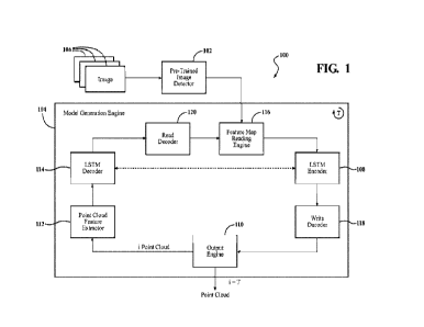
[0007] FIGURE 1 is a schematic view of a typical photovoltaic cell including
an active
layer according to some embodiments of the present disclosure.
[0008] FIGURE 2 is a stylized diagram showing components of an example PV
device
according to some embodiments of the present disclosure.
[0009] FIGURE 3 is a stylized diagram showing components of an example device
according to some embodiments of the present disclosure.
[0010] FIGURE 4 is a stylized diagram showing components of an example device
according to some embodiments of the present disclosure.
[0011] FIGURE 5 is a stylized diagram showing an illustration of a Ruddlesden-
Popper
perovskite.
CA 03159526 2022-5-25
WO 2021/108317
PCT/US2020/061824
4
[0012] FIGURE 6 is a stylized diagram showing an illustration of a perovskite
material
with addition of an alkyl ammonium cation according to some embodiments of the
present
disclosure.
[0013] FIGURE 7 is a stylized diagram showing an illustration of a perovskite
material
with a 1-butylammonium surface layer according to some embodiments of the
present disclosure.
[0014] FIGURE 8 is a stylized diagram showing an illustration of a perovskite
material
with a surface layer of multiple bulky organic cations according to some
embodiments of the
present disclosure.
[0015] FIGURE 8A is a stylized diagram showing an illustration of a perovskite
material
with a surface layer of multiple bulky organic cations according to some
embodiments of the
present disclosure.
[0016] FIGURE 9 is an illustration of a comparison of images taken of a
perovskite
material with and without a 1-butylammonium ("BAI") surface coating according
to some
embodiments of the present disclosure.
[0017] FIGURE 10 is a stylized diagram showing an illustration of a comparison
of images
taken of a perovskite material with and without a 1-butylammonium ("BAI")
surface coating
according to some embodiments of the present disclosure.
[0018] FIGURES 11A-D illustrate various perylene monoimides and diimides that
may be
applied to the surface of a perovskite material according to some embodiments
of the present
disclosure.
[0019] FIGURE 12 is a stylized diagram showing an illustration of a perovskite
material
with addition of a perylene monoimides ammonium cation according to some
embodiments of the
present disclosure.
[0020] FIGURE 13 is a stylized diagram showing an illustration of 1,4-
diammonium
butane incorporated into the crystal lattice of a formamidinium lead iodide
perovskite material
according to some embodiments of the present disclosure.
[0021] FIGURE 14 is an illustration of x-ray diffraction peaks (CRD) for
perovskite
having various concentrations of 1,4-diammonium butane according to some
embodiments of the
present disclosure.
[0022] FIGURE 15 provides images of perovskite material samples having various
concentrations of 1,4-diammonium butane over time according to some
embodiments of the
present disclosure.
[0023] FIGURE 16 provides illustrations of poly-ammonium alkyl cations,
according to
some embodiments of the present disclosure.
CA 03159526 2022-5-25
WO 2021/108317
PCT/US2020/061824
[0024] FIGURE 16A is a stylized diagram showing an illustration of 1,8
diammonium
octane incorporated into the crystal lattice of a formamidinium lead iodide
perovskite material
according to some embodiments of the present disclosure.
[0025] FIGURE 16B is a stylized diagram showing an illustration of bis(4-
aminobuty1)-
5
ammonium incorporated into the
crystal lattice of a formamidinium lead iodide perovskite material
according to some embodiments of the present disclosure.
[0026] FIGURE 16C is a stylized diagram showing an illustration of tris(4-
aminobuty1)-
ammonium incorporated into the crystal lattice of a formamidinium lead iodide
perovskite material
according to some embodiments of the present disclosure.
[0027] FIGURES 17-28 provide illustrations of the structures of certain
organic molecules,
according to some embodiments of the present disclosure.
[0028] FIGURE 29 illustrates x-ray diffraction patterns of perovskites
materials according
to some embodiments of the present disclosure.
[0029] FIGURE 30 provides a stylized illustration of thicknesses of inorganic
metal halide
sublattices of perovskite materials according to some embodiments of the
present disclosure.
[0030] FIGURE 31 shows optical and photoluminescence images of perovskite
material
photovoltaic devices according to some embodiments of the present disclosure.
[0031] FIGURE 32 illustrates power output curves of perovskite material
photovoltaic
devices according to some embodiments of the present disclosure.
[0032] FIGURE 33 illustrates current-voltage (I-V) scans of perovskite
material
photovoltaic devices according to some embodiments of the present disclosure.
[0033] FIGURE 34 illustrates box plots for open-circuit voltage (Voc), short-
circuit
current density (Jsc), Fill Factor (FE) and power conversion efficiency (PCE)
for perovskite
material photovoltaic devices according to some embodiments of the present
disclosure.
[0034] FIGURE 35 illustrates external quantum efficiency (EQE) curves of
perovskite
material photovoltaic devices according to some embodiments of the present
disclosure.
[0035] FIGURE 36 shows admittance spectroscopy plots of perovskite material
photovoltaic devices according to some embodiments of the present disclosure.
[0036] FIGURE 37 is a stylized illustration of a perovskite material device
3700
incorporating an NFA layer, according to certain embodiments.
[0037] FIGURES 38A and 38B illustrate the molecular structure of several NFA
compounds, according to some embodiments of the present disclosure.
[0038] FIGURE 39 provides an illustration of the synthesis reaction of a
functionalized
NDI molecule, according to some embodiments of the present disclosure.
CA 03159526 2022-5-25
WO 2021/108317
PCT/US2020/061824
6
[0039] FIGURE 40 illustrates molecular structures of two n-substituted
derivatives of
perylene diimide (PD!), according to some embodiments of the present
disclosure.
[0040] FIGURE 41 provides an illustration of a synthesis reaction for creating
DEAPPDI,
according to some embodiments of the present disclosure.
[0041] FIGURE 42 provides an illustration of a synthesis reaction for creating
TEAPPD1,
according to some embodiments of the present disclosure.
[0042] FIGURE 43 provides an illustration of the CyUNDI molecule, according to
some
embodiments of the present disclosure.
[0043] FIGURE 44 illustrates the molecular structure of compounds that may
function as
electron transport layers according to some embodiments of the present
disclosure
[0044] FIGURE 45 illustrates the molecular structure of compounds that may
function as
electron transport layers according to some embodiments of the present
disclosure.
[0045] FIGURE 46 illustrates energy levels for NDI compounds, according to
some
embodiments of the present disclosure.
[0046] FIGURE 47 illustrates energy levels for PDI compounds, according to
some
embodiments of the present disclosure.
[0047] FIGURE 48 illustrates energy levels for ITIC and IFICO compounds,
according to
some embodiments of the present disclosure.
DETAILED DESCRIPTION OF PREFERRED EMBODIMENTS
[0048] Improvements in various aspects of PV technologies compatible with
organic, non-
organic, and/or hybrid PVs promise to further lower the cost of both organic
PVs and other PVs.
For example, some solar cells, such as perovskite PV solar cells, may take
advantage of novel cost-
effective and high-stability alternative components, such as nickel oxide
interfacial layers. In
addition, various kinds of solar cells may advantageously include chemical
additives and other
materials that may, among other advantages, be more cost-effective and durable
than conventional
options currently in existence.
[0049] The present disclosure relates generally to compositions of matter,
apparatus and
methods of use of materials in photovoltaic cells in creating electrical
energy from solar radiation.
More specifically, this disclosure relates to photoactive and other
compositions of matter, as well
as apparatus, methods of use, and formation of such compositions of matter.
[0050] Some or all of materials in accordance with some embodiments of the
present
disclosure may also advantageously be used in any organic or other electronic
device, with some
examples including, but not limited to: batteries, field-effect transistors
(FETs), light-emitting
CA 03159526 2022-5-25
WO 2021/108317
PCT/US2020/061824
7
diodes (LEDs), non-linear optical devices, memristors, capacitors, rectifiers,
and/or rectifying
antennas.
[0051] In some embodiments, the present disclosure may provide PV and other
similar
devices (e.g., batteries, hybrid PV batteries, multi-junction PVs, FETs, LEDs,
x-ray detectors,
gamma ray detectors, photodiodes, CCDs, etc.). Such devices may in some
embodiments include
improved active material, interfacial layers (1FLs), and/or one or more
perovskite materials. A
perovskite material may be incorporated into various of one or more aspects of
a PV or other
device. A perovskite material according to some embodiments may be of the
general formula
CMX3, where: C comprises one or more cations (e.g., an amine, ammonium,
phosphonium, a
Group 1 metal, a Group 2 metal, and/or other cations or cation-like
compounds); M comprises one
or more metals (examples including Be, Mg, Ca, Sr, Ba, Fe, Cd, Co, Ni, Cu, Ag,
Au, Hg, Sn, Ge,
Ga, Pb, In, TI, Sb, Bi, Ti, Zn, Cd, Hg, and Zr); and X comprises one or more
anions. Perovskite
materials according to various embodiments are discussed in greater detail
below.
Photovoltaic Cells and Other Electronic Devices
[0052] Some PV embodiments may be described by reference to the illustrative
depictions
of solar cells as shown in FIG 1. An example PV architecture according to some
embodiments
may be substantially of the form substrate-anode-1FL-active layer-IFL-cathode.
The active layer
of some embodiments may be photoactive, and/or it may include photoactive
material. Other
layers and materials may be utilized in the cell as is known in the art.
Furthermore, it should be
noted that the use of the term "active layer" is in no way meant to restrict
or otherwise define,
explicitly or implicitly, the properties of any other layer ¨ for instance, in
some embodiments,
either or both IF Ls may also be active insofar as they may be semiconducting.
In particular,
referring to FIG. 1, a stylized generic PV cell 1000 is depicted, illustrating
the highly interfacial
nature of some layers within the PV. The PV 1000 represents a generic
architecture applicable to
several PV devices, such as perovskite material PV embodiments. The PV cell
1000 includes a
transparent substrate layer 1010, which may be glass (or a material similarly
transparent to solar
radiation) which allows solar radiation to transmit through the layer. The
transparent layer of some
embodiments may also be referred to as a superstrate or substrate (e.g., as
with substrate layer
3901 of FIG. 2), and it may comprise any one or more of a variety of rigid or
flexible materials
such as: glass, polyethylene, polypropylene, polycarbonate, polyimide, PMMA,
PET, PEN,
Kapton, or quartz. In general, the term substrate is used to refer to material
upon which the device
is deposited during manufacturing. The photoactive layer 1040 may be composed
of electron donor
or p-type material, and/or an electron acceptor or n-type material, and/or an
ambipolar
semiconductor, which exhibits both p- and n-type material characteristics,
and/or an intrinsic
CA 03159526 2022-5-25
WO 2021/108317
PCT/US2020/061824
8
semiconductor which exhibits neither n-type or p-type characteristics.
Photoactive layer 1040 may
be a perovskite material as described herein, in some embodiments. The active
layer or, as
depicted in FIG. 1, the photo-active layer 1040, is sandwiched between two
electrically conductive
electrode layers 1020 and 1060. In FIG. 1, the electrode layer 1020 may be a
transparent conductor
such as a tin-doped indium oxide (ITO material) or other material as described
herein. In other
embodiments second substrate 1070 and second electrode 1060 may be
transparent. As previously
noted, an active layer of some embodiments need not necessarily be
photoactive, although in the
device shown in FIG. 1, it is. The electrode layer 1060 may be an aluminum
material or other
metal, or other conductive materials such as carbon. Other materials may be
used as is known in
the art. The cell 1010 also includes an interfacial layer (IFL) 1030, shown in
the example of FIG.
1. The 1FL may assist in charge separation. In other embodiments, the IFL 1030
may comprise a
multi-layer 1FL, which is discussed in greater detail below. There also may be
an 1FL 1050
adjacent to electrode 1060. In some embodiments, the 1FL 1050 adjacent to
electrode 1060 may
also or instead comprise a multi-layer 1FL (again, discussed in greater detail
below). An 1FL
according to some embodiments may be semiconducting in character and may be
either intrinsic,
ambipolar, p-type, or n-type, or it may be dielectric in character. In some
embodiments, the 1FL
on the cathode side of the device (e.g., 1FL 1050 as shown in FIG. I) may be p-
type, and the 1FL
on the anode side of the device (e.g., 1FL 1030 as shown in FIG. 1) may be n-
type. In other
embodiments, however, the cathode-side FL may be n-type and the anode-side 1FL
may be p-
type. The cell 1010 may be attached to electrical leads by electrodes 1060 and
1020 and a
discharge unit, such as a battery, motor, capacitor, electric grid, or any
other electrical load.
[0053] Various embodiments of the present disclosure provide improved
materials and/or
designs in various aspects of solar cell and other devices, including among
other things, active
materials (including hole-transport and/or electron-transport layers),
interfacial layers, and overall
device design.
Interfacial Layers
[0054] The present disclosure, in some embodiments, provides advantageous
materials and
designs of one or more interfacial layers within a PV, including thin-coat
1FLs. Thin-coat liFts
may be employed in one or more IFLs of a PV according to various embodiments
discussed herein.
[0055] According to various embodiments, devices may optionally include an
interfacial
layer between any two other layers and/or materials, although devices need not
contain any
interfacial layers. For example, a perovskite material device may contain
zero, one, two, three,
four, five, or more interfacial layers (such as the example device of FIG. 2,
which contains five
interfacial layers 3903, 3905, 3907, 3909, and 3911). An interfacial layer may
include any suitable
CA 03159526 2022-5-25
WO 2021/108317
PCT/US2020/061824
9
material for enhancing charge transport and/or collection between two layers
or materials; it may
also help prevent or reduce the likelihood of charge recombination once a
charge has been
transported away from one of the materials adjacent to the interfacial layer.
An interfacial layer
may additionally physically and electrically homogenize its substrates to
create variations in
substrate roughness, dielectric constant, adhesion, creation or quenching of
defects (e.g., charge
traps, surface states). Suitable interfacial materials may include any one or
more of Ag; Al; Au;
B; Hi; Ca; Cd; Ce; Co; Cu; Fe; Ga; Ge; 11; In; Mg; Mn; Mo; Nb; Ni; Pt; Sb; Sc;
Si; Sn; To; Ti; V;
W; Y; Zn; Zr; carbides of any of the foregoing metals (e.g., SiC, Fe3C, WC,
VC, MoC, NbC);
suicides of any of the foregoing metals (e.g., Mg2Si, SrSi2, Sn2Si); oxides of
any of the foregoing
metals (e.g., alumina, silica, titania, Sn02, ZnO, NiO, ZrO2, Hf02), include
transparent conducting
oxides ("TCOs") such as indium tin oxide, aluminum doped zinc oxide (AZO),
cadmium oxide
(CdO), and fluorine doped tin oxide (FT0); sulfides of any of the foregoing
metals (e.g., CdS,
MoS2, SnS2); nitrides of any of the foregoing metals (e.g., GaN, Mg3N2, TiN,
BN, Si3N4);
selenides of any of the foregoing metals (e.g., CdSe, FeSe2, ZnSe); tellurides
of any of the
foregoing metals (e.g., CdTe, TiTe2, ZnTe); phosphides of any of the foregoing
metals (e.g., InP,
GaP, GaInP); arsenides of any of the foregoing metals (e.g., CoAs3, GaAs,
InGaAs, NiAs) ;
antimonides of any of the foregoing metals (e.g., AlSb, GaSb, InSb); halides
of any of the
foregoing metals (e.g., CuCl, CuI, Bib); pseudohalides of any of the foregoing
metals (e.g.,
CuSCN, AuCN, Fe(SCN)2); carbonates of any of the foregoing metals (e.g.,
CaCO3, Ce2(CO3)3);
functionalized or non-functionalized alkyl silyl groups; graphite; graphene;
fullerenes; carbon
nanotubes; any mesoporous material and/or interfacial material discussed
elsewhere herein; and
combinations thereof (including, in some embodiments, bilayers, trilayers, or
multi-layers of
combined materials). In some embodiments, an interfacial layer may include
perovskite material.
Further, interfacial layers may comprise doped embodiments of any interfacial
material mentioned
herein (e.g., Y-doped ZnO, N-doped single-wall carbon nanotubes). Interfacial
layers may also
comprise a compound having three of the above materials (e.g., CuTiO3,Zn2Sn04)
or a compound
having four of the above materials (e.g., CoNiZn0). The materials listed above
may be present in
a planar, mesoporous or otherwise nano-structured form (e.g. rods, spheres,
flowers, pyramids), or
aerogel structure.
[0056] First, as previously noted, one or more IFLs (e.g., either or both IFLs
2626 and
2627 as shown in FIG. 1) may comprise a photoactive organic compound of the
present disclosure
as a self-assembled monolayer (SAM) or as a thin film. When a photoactive
organic compound
of the present disclosure is applied as a SAM, it may comprise a binding group
through which it
may be covalently or otherwise bound to the surface of either or both of the
anode and cathode.
CA 03159526 2022-5-25
WO 2021/108317
PCT/US2020/061824
The binding group of some embodiments may comprise any one or more of COOH,
SiX3 (where
X may be any moiety suitable for forming a ternary silicon compound, such as
Si(OR)3 and SiC13),
S03, PO4H, OH, CH2X (where X may comprise a Group 17 halide), and 0. The
binding group
may be covalently or otherwise bound to an electron-withdrawing moiety, an
electron donor
5 moiety, and/or a core moiety. The binding group may attach to the
electrode surface in a manner
so as to form a directional, organized layer of a single molecule (or, in some
embodiments, multiple
molecules) in thickness (i.e., where multiple photoactive organic compounds
are bound to the
anode and/or cathode). As noted, the SAM may attach via covalent interactions,
but in some
embodiments, it may attach via ionic, hydrogen-bonding, and/or dispersion
force (i.e., Van Der
10 Waals) interactions. Furthermore, in certain embodiments, upon light
exposure, the SAM may
enter into a zwitterionic excited state, thereby creating a highly-polarized
1FL, which may direct
charge carriers from an active layer into an electrode (e.g., either the anode
or cathode). This
enhanced charge-carrier injection may, in some embodiments, be accomplished by
electronically
poling the cross-section of the active layer and therefore increasing charge-
carrier drift velocities
towards their respective electrode (e.g., hole to anode; electrons to
cathode). Molecules for anode
applications of some embodiments may comprise tunable compounds that include a
primary
electron donor moiety bound to a core moiety, which in turn is bound to an
electron-withdrawing
moiety, which in turn is bound to a binding group. In cathode applications
according to some
embodiments, 1FL molecules may comprise a tunable compound comprising an
electron poor
moiety bound to a core moiety, which in turn is bound to an electron donor
moiety, which in turn
is bound to a binding group. When a photoactive organic compound is employed
as an 1FL
according to such embodiments, it may retain photoactive character, although
in some
embodiments it need not be photoactive
[0057] Metal oxides may be used in thin film 1FLs of some embodiments and may
include
semiconducting metal oxides, such as NiO, SnO2 W03, V205, or Mo03. The
embodiment wherein
the second (e.g., n-type) active material comprises TiO2 coated with a thin-
coat IFL comprising
Al2O3 could be formed, for example, with a precursor material such as
Al(NO3)30xH20, or any
other material suitable for depositing A1203 onto the TiO2, followed by
thermal annealing and dye
coating. In example embodiments wherein a Moth coating is instead used, the
coating may be
formed with a precursor material such as Na2M04=21120; whereas a V205 coating
according to
some embodiments may be formed with a precursor material such as NaV03; and a
W03 coating
according to some embodiments may be formed with a precursor material such as
NaW0rH20.
The concentration of precursor material (e.g., Al(NO3)3exH20) may affect the
final film thickness
(here, of A1203) deposited on the TiO2 or other active material. Thus,
modifying the concentration
CA 03159526 2022-5-25
WO 2021/108317
PCT/US2020/061824
11
of precursor material may be a method by which the final film thickness may be
controlled. For
example, greater film thickness may result from greater precursor material
concentration. Greater
film thickness may not necessarily result in greater PCE in a PV device
comprising a metal oxide
coating. Thus, a method of some embodiments may include coating a TiO2 (or
other mesoporous)
layer using a precursor material having a concentration in the range of
approximately 0.5 to 10.0
mM; other embodiments may include coating the layer with a precursor material
having a
concentration in the range of approximately 2.0 to 6+0 mM; or, in other
embodiments,
approximately 2.5 to 5.5 mM.
[0058] Furthermore, although referred to herein as A1203 and/or alumina, it
should be
noted that various ratios of aluminum and oxygen may be used in forming
alumina. Thus, although
some embodiments discussed herein are described with reference to A1203, such
description is not
intended to define a required ratio of aluminum in oxygen. Rather, embodiments
may include any
one or more aluminum-oxide compounds, each having an aluminum oxide ratio
according to
A1x0y, where x may be any value, integer or non-integer, between approximately
1 and 100. In
some embodiments, x may be between approximately 1 and 3 (and, again, need not
be an integer).
Likewise, y may be any value, integer or non-integer, between 0.1 and 100. In
some embodiments,
y may be between 2 and 4 (and, again, need not be an integer). In addition,
various crystalline
forms of Alx0y may be present in various embodiments, such as alpha, gamma,
and/or amorphous
forms of alumina.
[0059] Likewise, although referred to herein as NiO, Mo03, W03, and V205, such
compounds may instead or in addition be represented as NiO y Mox0y, Wx0y, and
Vx0y,
respectively. Regarding each of Mox0y and Wx0y, x may be any value, integer or
non-integer,
between approximately 0.5 and 100; in some embodiments, it may be between
approximately 0.5
and 1.5. Likewise, y may be any value, integer or non-integer, between
approximately 1 and 100.
In some embodiments, y may be any value between approximately 1 and 4.
Regarding Vx0y, x
may be any value, integer or non-integer, between approximately 0.5 and 100;
in some
embodiments, it may be between approximately 0.5 and 1.5. Likewise, y may be
any value, integer
or non-integer, between approximately 1 and 100; in certain embodiments, it
may be an integer or
non-integer value between approximately 1 and 10. In some embodiments, x and y
may have
values so as to be in a non-stoichiometric ratio. It is noted that any TEL
materials written as
stoichiometric formulations in the present disclosure may also exist in non-
stoichiometric
formulations such as examples described above.
[0060] In some embodiments, the IFL may comprise a titanate. A titanate
according to
some embodiments may be of the general formula M'TiO3, where M' comprises any
2+ cation.
CA 03159526 2022-5-25
WO 2021/108317
PCT/US2020/061824
12
In some embodiments, M' may comprise a cationic form of Be, Mg, Ca, Sr, Ba,
Ni, Zn, Cd, Hg,
Cu, Pd, Pt, Sn, or Pb. In some embodiments, the 1FL may comprise a single
species of titanate,
which in other embodiments, the IFL may comprise two or more different species
of titanates. In
one embodiment, the titanate has the formula SrTiO3. In another embodiment,
the titanate may
have the formula BaTiO3. In yet another embodiment, the titanate may have the
formula CaTiO3.
[0061] By way of explanation, and without implying any limitation, titanates
have a
perovskite crystalline structure and strongly seed the perovskite material
(e.g., methylammonium
lead iodide (MAPbI3), and formamidinium lead iodide (FAPbI3)) growth
conversion process.
Titanates generally also meet other [FL requirements, such as ferroelectric
behavior, sufficient
charge carrier mobility, optical transparency, matched energy levels, and high
dielectric constant.
[0062] In other embodiments, the IFL may comprise a zirconate. A zirconate
according
to some embodiments may be of the general formula MiZr03, where W comprises
any 2+ cation.
In some embodiments, M' may comprise a cationic form of Be, Mg, Ca, Sr, Ba,
Ni, Zn, Cd, Hg,
Cu, Pd, Pt, Sn, or Pb. In some embodiments, the IFL may comprise a single
species of zirconate,
which in other embodiments, the tEL may comprise two or more different species
of zirconate. In
one embodiment, the zirconate has the formula SrZr03. In another embodiment,
the zirconate may
have the formula BaZr03. In yet another embodiment, the zirconate may have the
formula
CaZr03.
[0063] By way of explanation, and without implying any limitation, zirconates
have a
perovskite crystalline structure and strongly seed the perovskite material
(e.g., MAPbI3, FAPbI3)
growth conversion process. Zirconates generally also meet other IFL
requirements, such as
ferroelectric behavior, sufficient charge carrier mobility, optical
transparency, matched energy
levels, and high dielectric constant.
[0064] In other embodiments, the IFL may comprise a stannate. A stannate
according to
some embodiments may be of the general formula M'Sn03, or M'2SnO4where M'
comprises any
2+ cation. In some embodiments, W may comprise a cationic form of Be, Mg, Ca,
Sr, Ba, Ni,
Zn, Cd, Hg, Cu, Pd, Pt, Sn, or Pb. In some embodiments, the IFL may comprise a
single species
of stannate, which in other embodiments, the IFL may comprise two or more
different species of
stannate. In one embodiment, the stannate has the formula SrSn03. In another
embodiment, the
stannate may have the formula BaSn03. In yet another embodiment, the stannate
may have the
formula CaSn03.
[0065] By way of explanation, and without implying any limitation, stannates
have a
perovskite crystalline structure and strongly seed the perovskite material
(e.g., MAPbI3, FAPbb)
growth conversion process. Stannates generally also meet other IFL
requirements, such as
CA 03159526 2022-5-25
WO 2021/108317
PCT/US2020/061824
13
ferroelecuic behavior, sufficient charge carrier mobility, optical
transparency, matched energy
levels, and high dielectric constant.
[0066] In other embodiments, the IFL may comprise a plumbate. A plumbate
according
to some embodiments may be of the general formula M'Pb03, where M' comprises
any 2+ cation.
In some embodiments, M' may comprise a cationic form of Be, Mg, Ca, Sr, Ba,
Ni, Zn, Cd, Hg,
Cu, Pd, Pt, Sn, or Pb. In some embodiments, the IFL may comprise a single
species of plumbate,
which in other embodiments, the IFL may comprise two or more different species
of plumbate. In
one embodiment, the plumbate has the formula SrPb03. In another embodiment,
the plumbate
may have the formula BaPb03. In yet another embodiment, the plumbate may have
the formula
CaPb03. In yet another embodiment, the plumbate may have the formula
Pb"Pb1103.
[0067] By way of explanation, and without implying any limitation, plumbates
have a
perovskite crystalline structure and strongly seed the perovskite material
(e.g., MAPbI3, FAPM3)
growth conversion process. Plumbates generally also meet other IFL
requirements, such as
ferroelecuic behavior, sufficient charge carrier mobility, optical
transparency, matched energy
levels, and high dielectric constant.
[0068] Further, in other embodiments, an 1FL may comprise a combination of a
zirconate
and a titanate in the general formula MIZr1Tii,]03, where X is greater than 0
but less than one
1, and M' comprises any 2+ cation. In some embodiments, M' may comprise a
cationic form of
Be, Mg, Ca, Sr, Ba, Ni, Zn, Cd, Hg, Cu, Pd, Pt, Sn, or Pb. In some
embodiments, the IFL may
comprise a single species of zirconate, which in other embodiments, the IFL
may comprise two or
more different species of zirconate. In one embodiment, the zirconate/titanate
combination has
the formula Pb[Zrifii-x]03. In another embodiment, the zirconate/titanate
combination has the
formula Pb[Zro.52.Tio.43]03.
[0069] By way of explanation, and without implying any limitation, a
zirconate/titanate
combination have a perovskite crystalline structure and strongly seed the
perovskite material (e.g.,
MAPbI3, FAMI3) growth conversion process. Zirconate/titanate combinations
generally also
meet other IFL requirements, such as ferroelectric behavior, sufficient charge
carrier mobility,
optical transparency, matched energy levels, and high dielectric constant.
[0070] In other embodiments, the IFL may comprise a niobate. A niobate
according to
some embodiments may be of the general formula M'Nb03, where: M' comprises any
1+ cation.
In some embodiments, M' may comprise a cationic form of Li, Na, K, Rb, Cs, Cu,
Ag, Au, TI,
ammonium, or H. In some embodiments, the IFL may comprise a single species of
niobate, which
in other embodiments, the IFL may comprise two or more different species of
niobate. In one
CA 03159526 2022-5-25
WO 2021/108317
PCT/US2020/061824
14
embodiment, the niobate has the formula LiNb03. In another embodiment, the
niobate may have
the formula NaNb03. In yet another embodiment, the niobate may have the
formula AgNb03.
[0071] By way of explanation, and without implying any limitation, niobates
generally
meet IFL requirements, such as piezoelectric behavior, non-linear optical
polarizability,
photoelasticity, ferroelectric behavior, Pockets effect, sufficient charge
carrier mobility, optical
transparency, matched energy levels, and high dielectric constant.
[0072] In one embodiment, a perovskite material device may be formulated by
casting PbI2
onto a SrTiO3-coated ITO substrate. The PbI2 may be converted to MAPbI3 by a
dipping process.
This process is described in greater detail below. This resulting conversion
of PbI2 to MAPbI3 is
more complete (as observed by optical spectroscopy) as compared to the
preparation of the
substrate without SrTiO3.
[0073] Any interfacial material discussed herein may further comprise doped
compositions. To modify the characteristics (e.g., electrical, optical,
mechanical) of an interfacial
material, a stoichiometric or non-stoichiometric material may be doped with
one or more elements
(e.g., Na, Y, Mg, N, P) in amounts ranging from as little as 1 ppb to 50 mol%.
Some examples of
interfacial materials include: NiO, TiO2, SrTiO3, A1203, ZrO2, W03, V205, M03,
ZnO, graphene,
and carbon black. Examples of possible dopants for these interfacial materials
include: Li, Na, Be,
Mg, Ca, Sr, Ba, Sc, Y, Nb, Ti, Fe, Co, Ni, Cu, Ga, Sn, In, B, N, P. C, 5, As,
a halide, a pseudohalide
(e.g., cyanide, cyanate, isocyanate, fulminate, thiocyanate, isothiocyanate,
azide,
tetracarbonylcobaltate, carbamoyldicyanomethanide, dicyanonitrosomethanide,
dicyanamide, and
tricyanomethanide), and Al in any of its oxidation states. References herein
to doped interfacial
materials are not intended to limit the ratios of component elements in
interfacial material
compounds.
[0074] In some embodiments, multiple IFLs made from different materials may be
arranged adjacent to each other to form a composite IFL. This configuration
may involve two
different IFLs, three different IFLs, or an even greater number of different
IFLs. The resulting
multi-layer IFL or composite IFL may be used in lieu of a single-material 1FL.
For example, a
composite IFL may be used any IFL shown in the example of FIG. 2, such as IFL
3903, IFL 3905,
[FL 3907, IFL 3909, or IFL 3911. While the composite IFL differs from a single-
material IFL,
the assembly of a perovskite material PV cell having multi-layer IFLs is not
substantially different
than the assembly of a perovskite material PV cell having only single-material
IFLs.
[0075] Generally, the composite IFL may be made using any of the materials
discussed
herein as suitable for an IFL. In one embodiment, the IFL comprises a layer of
A1203 and a layer
of ZnO or M:ZnO (doped ZnO, e.g., Be:ZnO, Mg:ZnO, Ca:ZnO, Sr2n0, Ba:ZnO,
Sc:ZnO,
CA 03159526 2022-5-25
WO 2021/108317
PCT/US2020/061824
Y:ZnO, Nbin0). In an embodiment, the [FL comprises a layer of ZrO2 and a layer
of ZnO or
M:ZnO. In certain embodiments, the IFL comprises multiple layers. In some
embodiments, a
multi-layer IFL generally has a conductor layer, a dielectric layer, and a
semi-conductor layer. In
particular embodiments the layers may repeat, for example, a conductor layer,
a dielectric layer, a
5 semi-conductor layer, a dielectric layer, and a semi-conductor layer.
Examples of multi-layer
IFLs include an IFL having an ITO layer, an A1203 layer, a ZnO layer, and a
second A1203 layer;
an JUL having an ITO layer, an Al2O3 layer, a ZnO layer, a second Al2O3 layer,
and a second ZnO
layer; an IFL having an ITO layer, an A1203 layer, a ZnO layer, a second A1203
layer, a second
ZnO layer, and a third M203 layer; and 1FLs having as many layers as necessary
to achieve the
10 desired performance characteristics. As discussed previously, references
to certain stoichiometric
ratios are not intended to limit the ratios of component elements in IFL
layers according to various
embodiments.
[0076] Arranging two or more adjacent IFLs as a composite JUL may outperform a
single
IFL in perovskite material PV cells where attributes from each IFL material
may be leveraged in
15 a single IFL. For example, in the architecture having an ITO layer, an
A1203 layer, and a ZnO
layer, where ITO is a conducting electrode, A1203 is a dielectric material and
ZnO is a n-type
semiconductor, ZnO acts as an electron acceptor with well performing electron
transport properties
(e.g., mobility). Additionally, A1203 is a physically robust material that
adheres well to ITO,
homogenizes the surface by capping surface defects (e.g., charge traps), and
improves device diode
characteristics through suppression of dark current.
[0077] Additionally, some perovskite material PV cells may include so called
"tandem"
PV cells having more than one perovskite photoactive layer. For example, both
photoactive
materials 3908 and 3906 of FIG. 2 may be perovskite materials. In such tandem
PV cells an
interfacial layer between the two photoactive layers, such as IFL 3907 (i.e.,
a recombination layer)
of FIG. 2 may comprise a multi-layer, or composite, IFL. In some embodiments,
the layers
sandwiched between the two photoactive layers of a tandem PV device may
include an electrode
layer.
[0078] A tandem Mt device may include the following layers, listed in order
from either
top to bottom or bottom to top: a first substrate, a first electrode, a first
interfacial layer, a first
perovskite material, a second interfacial layer, a second electrode, a third
interfacial layer, a second
perovskite material, a fourth interfacial layer, and a third electrode. In
some embodiments, the
first and third interfacial layers may be hole transporting interfacial layers
and the second and
fourth interfacial layers may be electron transporting interfacial layers. In
other embodiments, the
first and third interfacial layers may be electron transporting interfacial
layers and the second and
CA 03159526 2022-5-25
WO 2021/108317
PCT/US2020/061824
16
fourth interfacial layers may be hole transporting interfacial layers. In yet
other embodiments, the
first and fourth interfacial layers may be hole transporting interfacial
layers and the second and
third interfacial layers may be electron transporting interfacial layers. In
other embodiments, the
first and fourth interfacial layers may be electron transporting interfacial
layers and the second and
third interfacial layers may be hole transporting interfacial layers. In
tandem PV devices the first
and second perovskite materials may have different band gaps. In some
embodiments, the first
perovskite material may be forinatnidinium lead bromide (FAPbBr3) and the
second perovskite
material may be formamidinium lead iodide (FAPbI3). In other embodiments, the
first perovskite
material may be methylammonium lead bromide (MAPbBr3) and the second
perovskite material
may be formamidinium lead iodide (FAPbI3). In other embodiments, the first
perovskite material
may be methylammonium lead bromide (MAPbBr3) and the second perovskite
material may be
methylammonium lead iodide (MAP1:43).
Perovskite Material
[0079] A perovskite material may be incorporated into one or more aspects of a
PV or
other device. A perovskite material according to some embodiments may be of
the general formula
CwMyXz, where: C comprises one or more cations (e.g., an amine, ammonium,
phosphonium, a
Group 1 metal, a Group 2 metal, and/or other cations or cation-like
compounds); M comprises one
or more metals (examples including Be, Mg, Ca, Sr, Ba, Fe, Cd, Co, Ni, Cu, Ag,
Au, Hg, Sn, Ge,
Ga, Pb, In, T1, Sb, Bi, Ti, Zn, Cd, Hg, and Zr); X comprises one or more
anions; and w, y, and z
represent real numbers between 1 and 20. In some embodiments, C may include
one or more
organic cations. In some embodiments, each organic cation C may be larger than
each metal M,
and each anion X may be capable of bonding with both a cation C and a metal M.
In particular
embodiments, a perovskite material may be of the formula CMX3.
[0080] In certain embodiments, C may include an ammonium, an organic cation of
the
general formula [N1t4] where the R groups may be the same or different groups.
Suitable R
groups include, but are not limited to: hydrogen, methyl, ethyl, propyl,
butyl, pentyl group or
isomer thereof; any alkane, alkene, or alkyne CxHy, where x = 1 - 20, y = 1 -
42, cyclic, branched
or straight-chain; alkyl halides, CxHyXz, x = 1 - 20, y = 0 - 42, z = 1 - 42,
X = F, Cl, Br, or I; any
aromatic group (e.g., phenyl, alkylphenl, alkoxyphenyl, pyridine,
naphthalene); cyclic complexes
where at least one nitrogen is contained within the ring (e.g., pyridine,
pyrrole, pyrrolidine,
piperidine, tetrahydroquinoline), any sulfur-containing group (e.g.,
sulfoxide, thiol, alkyl sulfide);
any nitrogen-containing group (nitroxide, amine); any phosphorous containing
group (phosphate);
any boron-containing group (e.g., boronic acid); any organic acid (e.g.,
acetic acid, propanoic
acid); and ester or amide derivatives thereof; any amino acid (e.g., glycine,
cysteine, praline,
CA 03159526 2022-5-25
WO 2021/108317
PCT/US2020/061824
17
glutamic acid, arginine, serine, histidine, 5-ammoniumvaleric acid) including
alpha, beta, gamma,
and greater derivatives; any silicon containing group (e.g., siloxane); and
any alkoxy or group, -
0CxHy, where x = 0 - 20, y = 1 - 42.
[0081] In certain embodiments, C may include a formamidinium, an organic
cation of the
general formula [R2NCRNR2] where the R groups may be the same or different
groups. Suitable
R groups include, but are not limited to: hydrogen, methyl, ethyl, propyl,
butyl, pentyl group or
isomer thereof; any alkane, a1kene, or alkyne CxHy, where x = 1 - 20, y = 1 -
42, cyclic, branched
or straight-chain; alkyl halides, CxHyXz, x = 1 - 20, y = 0 - 42, z = 1 - 42,
X = F, Cl, Br, or 1; any
aromatic group (e.g., phenyl, alkylphenl, alkoxyphenyl, pyridine,
naphthalene); cyclic complexes
where at least one nitrogen is contained within the ring (e.g., imidazole,
benzimidazole,
pyrimidine, (azolidinylidenemethyppyrrolidine, triazole); any sulfur-
containing group (e.g.,
sulfoxide, thiol, alkyl sulfide); any nitrogen-containing group (nitroxide,
amine); any phosphorous
containing group (phosphate); any boron-containing group (e.g., boronic acid);
any organic acid
(acetic acid, propanoic acid) and ester or amide derivatives thereof; any
amino acid (e.g., glycine,
cysteine, proline, glutamic acid, arginine, serine, histidine, 5-
ammoniumvaleric acid) including
alpha, beta, gamma, and greater derivatives; any silicon containing group (e g
, siloxane); and
any alkoxy or group, -0CxHy, where x =0 - 20, y = 1 - 42.
R5
R3
R4
Formula 1
[0082] Formula 1 illustrates the structure of a formamidinium cation having
the general
formula of [R2NCRNR2] as described above. Formula 2 illustrates examples
structures of several
formamidinium cations that may serve as a cation "C" in a perovskite material.
C
_see
N"-
ilythcrx-y-Rhydrc_txyz,uninanethylericiarninonitun
Methyl(methylatninomet by I cue )anarnonit un.
CA 03159526 2022-5-25
WO 2021/108317
PCT/US2020/061824
18
N
N'
eye !a he xy I- Royc 1 o liexyi anti xi J.)) meth y 1 en e. ai tu- no a in IT
t
40 .000.4...õ..===%.,,
I
N
Ani tinomethylenthenyl)arnmonium
I
0 is
0
Will..... `,..--=.t,,,%-..õ .
(Met ho xy ani I ino )rnethyl elle- (4- met hoxyphenyl ) arnmoni urn
11
S \
.,õ.....-- ..........%. -----...õ
N
N'
Thienyi-[(2--thieny1 OITI i II o)tnethytene]ananonium
Formula 2
[0083] In certain embodiments, C may include a guanidinium, an organic cation
of the
general formula [(R2N)2C=NR2] where the R groups may be the same or different
groups.
Suitable R groups include, but are not limited to: hydrogen, methyl, ethyl,
propyl, butyl, pentyl
group or isomer thereof; any alkane, alkene, or alkyne CxHy, where x = 1 - 20,
y = 1 - 42, cyclic,
branched or straight-chain; alkyl halides, CxHyXz, x = 1 - 20, y = 0 - 42, z =
1 - 42, X = F, Cl, Br,
or I; any aromatic group (e.g., phenyl, alkylphenyl, alkoxyphenyl, pyridine,
naphthalene); cyclic
complexes where at least one nitrogen is contained within the ring (e.g.,
octahydropyrimido[1,2-
a]pyrimidine, pyrimido[1,2-a]pyrimidine,
hexahydroimidazo[1,2-
a]imidazole,
hexahydropyrimidin-2-imine); any sulfur-containing group (e.g., sulfoxide,
thiol, alkyl sulfide);
any nitrogen-containing group (nitroxide, amine); any phosphorous containing
group (phosphate);
any boron-containing group (e.g., boronic acid); any organic acid (acetic
acid, propanoic acid) and
CA 03159526 2022-5-25
WO 2021/108317
PCT/US2020/061824
19
ester or amide derivatives thereof; any amino acid (e.g., glycine, cysteine,
proline, gjutamic acid,
arginine, serine, histidine, 5-ammoniumvaleric acid) including alpha, beta,
gamma, and greater
derivatives; any silicon containing group (e.g., siloxane); and any alkoxy or
group, -0CxHy,
where x = 0 - 20, y = 1 - 42.
R5 ... R6
,,,,,
N
RI. %%N.
R3
N
TN'
I
I
R.) R4
Formula 3
[0084] Formula 3 illustrates the structure of a guanidinium cation having the
general
formula of [(R2N)20=NR.21+ as described above. Formula 4 illustrates examples
of structures of
several guanidinium cations that may serve as a cation "C" in a perovskite
material.
NH-;
N
Ns
[..Amino(rn.ethytatningtrietbylenci-mettlykammonliant
NH,
F3C, A C F--
.0-
5
N
N.'
Ratino(triil uo.ro akethyi amino:0e hy lents+ (trifluaromethy ipaunorsium.
coN -----L"---tW
2 ,3,5,6-Te traby tiro- I II-Imidazof 1,2-al imidazol-7-ium
N.E12
A .
N
Nr
[Arnino--(cycloheryhmino)metityiene. -cyciolioxyl-aminonitun
CA 03159526 2022-5-25
WO 2021/108317
PCT/US2020/061824
1'1 1112, ....0
N
f Arnijlo-(2-tbieuyhrnino)rnethylenej(2-thi cut) SIT amoni/m3.
E.
l,iaNCI
N
N.......
[Amino (anilin Omethyiene]phenyl-arranonium
IVI:e0
.,....õ..3/4 OW 0
NH?
-es'e#L Nit I
00 '.4r
[Am ino-(4-methoxyani liTioyme.thylen.e}-(4-methoxyp.benyipnunaniurn
Formula 4
5
[0085] In certain embodiments, C
may include an ethene tetramine cation, an organic
cation of the general formula [(R2N)2C(NR.2)21+ where the R groups may be the
same or
different groups. Suitable R groups include, but are not limited to: hydrogen,
methyl, ethyl, propyl,
butyl, pentyl group or isomer thereof; any alkane, alkene, or alkyne Cx_fly,
where x = 1 - 20, y =
1 - 42, cyclic, branched or straight-chain; alkyl halides, CxHyXz, x = 1 - 20,
y = 0 - 42, z = 1 - 42,
10
X = F, Cl, Br, or I; any aromatic
group (e.g., phenyl, alkylphenl, alkoxyphenyl, pyridine,
naphthalene); cyclic complexes where at least one nitrogen is contained within
the ring (e.g., 2-
hexahydropyrimidin-2-ylidenehexahydropyrimidi ne,
octahydropyrazino[2,3-
14pyrazine,
pyrazino[2,3-14pyrazine, quinoxalino[2,3-b]quinoxaline); any sulfur-containing
group (e.g.,
sulfoxide, thiol, alkyl sulfide); any nitrogen-containing group (nitroxide,
amine); any phosphorous
15
containing group (phosphate); any
boron-containing group (e.g., boronic acid); any organic acid
(acetic acid, propanoic acid) and ester or amide derivatives thereof; any
amino acid (e.g., glycine,
cysteine, proline, glutamic acid, arginine, serine, histidine, 5-
ammoniumvaleric acid) including
alpha, beta, gamma, and greater derivatives; any silicon containing group
(e.g., siloxane); and
any alkoxy or group, -0CxHy, where x =0 - 20, y = 1 - 42.
CA 03159526 2022-5-25
WO 2021/108317
PCT/US2020/061824
21
R2 113
RI.¨ N
N-144
1)===(
R8¨ N
R7 R6
Formula 5
[0086] Formula 5 illustrates the structure of an ethene tetramine cation
having the general
formula of [(R2N)2C=C(NR2)2] as described above. Formula 6 illustrates
examples of structures
of several ethene tetramine ions that may serve as a cation "C" in a
perovskite material.
2-hexa1iydropyrimidin-2-ylidenehexahydropyrimidine
Ne).
pyrazino[2,3-b]py1a2.ine
C X
1. ,2,3,4,5õ6,7$-octallydropyrazino [2,3-b ]ayrazine
N
Or X
quinexalino[2,3-blquinexa1ine
Formula 6
CA 03159526 2022-5-25
WO 2021/108317
PCT/US2020/061824
22
[0087] In certain embodiments, C may include an imidazolium cation, an
aromatic, cyclic
organic cation of the general formula [CRNRCRNRCR] where the R groups may be
the same or
different groups. Suitable R groups may include, but are not limited to:
hydrogen, methyl, ethyl,
propyl, butyl, pentyl group or isomer thereof; any alkane, alkene, or alkyne
CxHy, where x = 1 -
20, y = 1 - 42, cyclic, branched or straight-chain; alkyl halides, CxHyXz, x =
1 - 20, y = 0 - 42, z
= 1 - 42, X = F, Cl, Br, or I; any aromatic group (e.g., phenyl, allcylphenyl,
alkoxyphenyl, pyridine,
naphthalene); cyclic complexes where at least one nitrogen is contained within
the ring (e g., 2-
hexahydropyri mi din-2-yli denehexahydropyrim i di ne,
octahydropyrazino[2,3-
b]pyrazine,
pyrazino[2,3-b]pyrazine, quinoxalino[2,3-b]quinoxaline); any sulfur-containing
group (e.g.,
sulfoxide, thiol, alkyl sulfide); any nitrogen-containing group (nitroxide,
amine); any phosphorous
containing group (phosphate); any boron-containing group (e.g., boronic acid);
any organic acid
(acetic acid, propanoic acid) and ester or amide derivatives thereof; any
amino acid (e.g., glycine,
cysteine, proline, glutamic acid, arginine, serine, histidine, 5-
ammoniumvaleric acid) including
alpha, beta, gamma, and greater derivatives; any silicon containing group
(e.g., siloxane); and
any alkoxy or group, -00cHy, where x =0 - 20, y = 1 - 42.
[0088] In certain embodiments, C may include a pyridium cation, an aromatic,
cyclic
organic cation of the general formula [CRCRCRCRCRNR] where the R groups may
be the same
or different groups. Suitable R groups may include, but are not limited to:
hydrogen, methyl, ethyl,
propyl, butyl, pentyl group or isomer thereof; any alkane, alkene, or alkyne
CxHy, where x = 1 -
20, y = 1 - 42, cyclic, branched or straight-chain; alkyl halides, OcHyXz, x =
1 - 20, y = 0 - 42, z
= 1 -42, X = F, Cl, Br, or I; any aromatic group (e.g., phenyl, alkylphenyl,
alkoxyphenyl, pyridine,
naphthalene); cyclic complexes where at least one nitrogen is contained within
the ring (e.g., 2-
hexahydropyri mi din-2-yli denehexahydropyrim i di ne,
octahydropyrazino[2,3-
b]pyrazine,
pyrazino[2,3-b]pyrazine, quinoxalino[2,3-b]quinoxaline); any sulfur-containing
group (e.g.,
sulfoxide, thiol, alkyl sulfide); any nitrogen-containing group (nitroxide,
amine); any phosphorous
containing group (phosphate); any boron-containing group (e.g., boronic acid);
any organic acid
(acetic acid, propanoic acid) and ester or amide derivatives thereof; any
amino acid (e.g., glycine,
cysteine, proline, glutamic acid, arginine, serine, histidine, 5-
ammoniumvaleric acid) including
alpha, beta, gamma, and greater derivatives; any silicon containing group
(e.g., siloxane); and
any alkoxy or group, -0CxHy, where x =0 - 20, y = 1 - 42.
CA 03159526 2022-5-25
WO 2021/108317
PCT/US2020/061824
23
Formula 7
[0089] In some embodiments, X may include one or more halides. In certain
embodiments, X may instead or in addition include a Group 16 anion. In certain
embodiments,
the Group 16 anion may be oxide, sulfide, selenide, or telluride. In certain
embodiments, X may
instead or in addition include one or more a pseudohalides (e.g., cyanide,
cyanate, isocyanate,
fulminate, thiocyanate, i sothiocyanate,
azide, tetracarbonylcobaltate,
carbamoyl dicyanomethani de, dicyanonitrosomethani de, di cyanami de, and tri
cyanomethani de).
[0090] In one embodiment, a perovskite material may comprise the empirical
formula
CMX3 where: C comprises one or more of the aforementioned cations, a Group 1
metal, a Group
2 metal, and/or other cations or cation-like compounds; M comprises one or
more metals
(examples including Be, Mg, Ca, Sr, Ba, Fe, Cd, Co, Ni, Cu, Ag, Au, Hg, Sn,
Ge, Ga, Pb, In, TI,
Sb, Bi, Ti, Zn, Cd, Hg, and Zr); and X comprises one or more of the
aforementioned anions.
[0091] In another embodiment, a perovskite material may comprise the empirical
formula
C'M2X6 where: C' comprises a cation with a 2+ charge including one or more of
the
aforementioned cations, diammonium butane, a Group 1 metal, a Group 2 metal,
and/or other
cations or cation-like compounds; M comprises one or more metals (examples
including Be, Mg,
Ca, Sr, Ba, Fe, Cd, Co, Ni, Cu, Ag, Au, Hg, Sn, Ge, Ga, Pb, In, TI, Sb, Bi,
Ti, Zn, Cd, Hg, and Zr);
and X comprises one or more of the aforementioned anions.
[0092] In another embodiment, a perovskite material may comprise the empirical
formula
C'MX4 where: C' comprises a cation with a 2+ charge including one or more of
the
aforementioned cations, diammonium butane, a Group 1 metal, a Group 2 metal,
and/or other
cations or cation-like compounds; M comprises one or more metals (examples
including Be, Mg,
Ca, Sr, Ba, Fe, Cd, Co, Ni, Cu, Ag, Au, Hg, Sn, Ge, Ga, Pb, In, TI, Sb, Bi,
Ti, Zn, Cd, Hg, and Zr);
and X comprises one or more of the aforementioned anions. In such an
embodiment, the
perovskite material may have a 2D structure.
CA 03159526 2022-5-25
WO 2021/108317
PCT/US2020/061824
24
[0093] In one embodiment, a perovskite material may comprise the empirical
formula
C3M2X9 where: C comprises one or more of the aforementioned cations, a Group 1
metal, a Group
2 metal, and/or other cations or cation-like compounds; M comprises one or
more metals
(examples including Be, Mg, Ca, Sr, Ba, Fe, Cd, Co, Ni, Cu, Ag, Au, Hg, Sn,
Ge, Ga, Pb, In, TI,
Sb, Hi, Ti, Zn, Cd, Hg, and Zr); and X comprises one or more of the
aforementioned anions.
[0094] In one embodiment, a perovskite material may comprise the empirical
formula
CM2X7 where: C comprises one or more of the aforementioned cations, a Group 1
metal, a Group
2 metal, and/or other cations or cation-like compounds; M comprises one or
more metals
(examples including Be, Mg, Ca, Sr, Ba, Fe, Cd, Co, Ni, Cu, Ag, Au, Hg, Sn,
Ge, Ga, Pb, In, TI,
Sb, Bi, Ti, Zn, Cd, Hg, and Zr n); and X comprises one or more of the
aforementioned anions.
[0095] In one embodiment, a perovskite material may comprise the empirical
formula
C2IvDC4 where: C comprises one or more of the aforementioned cations, a Group
1 metal, a Group
2 metal, and/or other cations or cation-like compounds; M comprises one or
more metals
(examples including Be, Mg, Ca, Sr, Ba, Fe, Cd, Co, Ni, Cu, Ag, Au, Hg, Sn,
Ge, Go, Pb, In, T1,
Sb, Di, Ti, Zn, Cd, Hg, and Zr); and X comprises one or more of the
aforementioned anions_
[0096] Perovskite materials may also comprise mixed ion formulations where C,
M, or X
comprise two or more species, for example, Cso.IFAo.9Pb(Io.9Clo.)3;
Rbo.1FAo.9Pboo.9Clo43
Cso.iFAo.9PbI3; FAPbo.5Sno.513; FAo.s3Cso.17Pb(IokBro.4)3;
FAo.s3Cso.12Rbo.o5Pb(Io.6Bro.4)3 and
FA0.85MAo.15Pb(Io.s5Bro.15)3.
Composite Perovskite Material Device Design
[0097] In some embodiments, the present disclosure may provide composite
design of PV
and other similar devices (e.g., batteries, hybrid PV batteries, FETs, LEDs,
nonlinear optics
(NLOs), waveguides, etc.) including one or more perovskite materials. For
example, one or more
perovskite materials may serve as either or both of first and second active
material of some
embodiments (e.g., active materials 3906a and 3908a of FIG. 3). In more
general terms, some
embodiments of the present disclosure provide PV or other devices having an
active layer
comprising one or more perovskite materials. In such embodiments, perovskite
material (that is,
material including any one or more perovskite materials(s)) may be employed in
active layers of
various architectures. Furthermore, perovskite material may serve the
function(s) of any one or
more components of an active layer (e.g., charge transport material,
mesoporous material,
photoactive material, and/or interfacial material, each of which is discussed
in greater detail
below). In some embodiments, the same perovskite materials may serve multiple
such functions,
although in other embodiments, a plurality of perovskite materials may be
included in a device,
each perovskite material serving one or more such functions. In certain
embodiments, whatever
CA 03159526 2022-5-25
WO 2021/108317
PCT/US2020/061824
role a perovskite material may serve, it may be prepared and/or present in a
device in various
states. For example, it may be substantially solid in some embodiments. A
solution or suspension
may be coated or otherwise deposited within a device (e.g., on another
component of the device
such as a mesoporous, interfacial, charge transport, photoactive, or other
layer, and/or on an
5 electrode). Perovskite materials in some embodiments may be formed in
situ on a surface of
another component of a device (e.g., by vapor deposition as a thin-film
solid). Any other suitable
means of forming a layer comprising perovskite material may be employed
[0098] In general, a perovskite material device may include a first electrode,
a second
electrode, and an active layer comprising a perovskite material, the active
layer disposed at least
10 partially between the first and second electrodes. In some embodiments,
the first electrode may
be one of an anode and a cathode, and the second electrode may be the other of
an anode and
cathode. An active layer according to certain embodiments may include any one
or more active
layer components, including any one or more of: charge transport material;
liquid electrolyte;
mesoporous material; photoactive material (e.g., a dye, silicon, cadmium
telluride, cadmium
15 sulfide, cadmium selenide, copper indium gallium selenide, gallium
arsenide, germanium indium
phosphide, semiconducting polymers, other photoactive materials)); and
interfacial material. Any
one or more of these active layer components may include one or more
perovskite materials. In
some embodiments, some or all of the active layer components may be in whole
or in part arranged
in sub-layers. For example, the active layer may comprise any one or more of:
an interfacial layer
20 including interfacial material; a mesoporous layer including mesoporous
material; and a charge
transport layer including charge transport material. Further, an interfacial
layer may be included
between any two or more other layers of an active layer according to some
embodiments and/or
between an active layer component and an electrode. Reference to layers herein
may include either
a final arrangement (e.g., substantially discrete portions of each material
separately definable
25 within the device), and/or reference to a layer may mean arrangement
during construction of a
device, notwithstanding the possibility of subsequent intermixing of
material(s) in each layer.
Layers may in some embodiments be discrete and comprise substantially
contiguous material (e.g.,
layers may be as stylistically illustrated in FIG. 2).
[0099] In some embodiments, a perovskite material device may be a field effect
transistor
(FET). An FET perovskite material device may include a source electrode, drain
electrode, gate
electrode, dielectric layer, and a semiconductor layer. In some embodiments
the semiconductor
layer of an FET perovskite material device may be a perovskite material.
[00100] A perovskite material device according to some embodiments may
optionally
include one or more substrates. In some embodiments, either or both of the
first and second
CA 03159526 2022-5-25
WO 2021/108317
PCT/US2020/061824
26
electrode may be coated or otherwise disposed upon a substrate, such that the
electrode is disposed
substantially between a substrate and the active layer. The materials of
composition of devices
(e.g., substrate, electrode, active layer and/or active layer components) may
in whole or in part be
either rigid or flexible in various embodiments. In some embodiments, an
electrode may act as a
substrate, thereby negating the need for a separate substrate.
[00101] Furthermore, a perovskite material device according to certain
embodiments may
optionally include an anti-reflective layer or anti-reflective coating (ARC).
In addition, a
perovskite material device may include any one or more additives, such as any
one or more of the
additives discussed above with respect to some embodiments of the present
disclosure.
[00102] Description of some of the various materials that may be included in a
perovskite
material device will be made in part with reference to FIG. 2. FIG. 2 is a
stylized diagram of a
perovskite material device 3900 according to some embodiments. Although
various components
of the device 3900 are illustrated as discrete layers comprising contiguous
material, it should be
understood that FIG. 2 is a stylized diagram; thus, embodiments in accordance
with it may include
such discrete layers, and/or substantially intermixed, non-contiguous layers,
consistent with the
usage of "layers" previously discussed herein. The device 3900 includes first
and second
substrates 3901 and 3913. A first electrode 3902 is disposed upon an inner
surface of the first
substrate 3901, and a second electrode 3912 is disposed on an inner surface of
the second substrate
3911 An active layer 3950 is sandwiched between the two electrodes 3902 and
3912. The active
layer 3950 includes a mesoporous layer 3904; first and second photoactive
materials 3906 and
3908; a charge transport layer 3910, and several interfacial layers. FIG. 2
furthermore illustrates
an example device 3900 according to embodiments wherein sub-layers of the
active layer 3950
are separated by the interfacial layers, and further wherein interfacial
layers are disposed upon
each electrode 3902 and 3912. In particular, second, third, and fourth
interfacial layers 3905, 3907,
and 3909 are respectively disposed between each of the mesoporous layer 3904,
first photoactive
material 3906, second photoactive material 3908, and charge transport layer
3910. First and fifth
interfacial layers 3903 and 3911 are respectively disposed between (i) the
first electrode 3902 and
mesoporous layer 3904; and (ii) the charge transport layer 3910 and second
electrode 3912. Thus,
the architecture of the example device depicted in FIG. 2 may be characterized
as: substrate-
electrode¨active layer¨electrode¨substrate. The architecture of the active
layer 3950 may be
characterized as: interfacial layer¨mesoporous layer¨interfacial
layer¨photoactive material¨
interfacial layer __________________ photoactive material _______ interfacial
layer¨charge transport layer ________________________ interfacial
layer. As noted previously, in some embodiments, interfacial layers need not
be present; or, one
CA 03159526 2022-5-25
WO 2021/108317
PCT/US2020/061824
27
or more interfacial layers may be included only between certain, but not all,
components of an
active layer and/or components of a device.
[00103] A substrate, such as either or both of first and second substrates
3901 and 3913,
may be flexible or rigid. If two substrates are included, at least one should
be transparent or
translucent to electromagnetic (EM) radiation (such as, e.g., UV, visible, or
IR radiation). If one
substrate is included, it may be similarly transparent or translucent,
although it need not be, so long
as a portion of the device permits FM radiation to contact the active layer
3950. Suitable substrate
materials include any one or more of: glass; sapphire; magnesium oxide (MgO);
mica; polymers
(e.g., PEN, PET, PEG, polyolefin, polypropylene, polyethylene, polycarbonate,
PMMA,
polyamide, vinyl, Kapton); ceramics; carbon; composites (e.g., fiberglass,
Kevlar; carbon fiber);
fabrics (e.g., cotton, nylon, silk, wool); wood; drywall; tiles (e.g. ceramic,
composite, or clay);
metal; steel; silver; gold; aluminum; magnesium; concrete; and combinations
thereof.
[00104] As previously noted, an electrode (e.g., one of electrodes 3902 and
3912 of FIG. 2)
may be either an anode or a cathode. In some embodiments, one electrode may
function as a
cathode, and the other may function as an anode. Either or both electrodes
3902 and 3912 may be
coupled to leads, cables, wires, or other means enabling charge transport to
and/or from the device
3900. An electrode may constitute any conductive material, and at least one
electrode should be
transparent or translucent to EM radiation, and/or be arranged in a manner
that allows EM radiation
to contact at least a portion of the active layer 3950. Suitable electrode
materials may include any
one or more of: indium tin oxide or tin-doped indium oxide (ITO); fluorine-
doped tin oxide (FT0);
cadmium oxide (CdO); zinc indium tin oxide (ZITO); aluminum zinc oxide (AZO);
aluminum
(Al); gold (Au); silver (Ag); calcium (Ca); chromium (Cr); copper (Cu);
magnesium (Mg);
titanium (Ti); steel; carbon (and allotropes thereof); doped carbon (e.g.,
nitrogen-doped);
nanoparticles in core-shell configurations (e.g., silicon-carbon core-shell
structure), and
combinations thereof
[00105] Mesoporous material (e.g., the material included in mesoporous layer
3904 of FIG.
2) may include any pore-containing material. In some embodiments, the pores
may have diameters
ranging from about 1 to about 100 nm; in other embodiments, pore diameter may
range from about
2 to about 50 nm. Suitable mesoporous material includes any one or more of:
any interfacial
material and/or mesoporous material discussed elsewhere herein; aluminum (Al);
bismuth (Bi);
cerium (Ce); hafnium (Hf); indium (In); molybdenum (Mo); niobium (Nb); nickel
(Ni); silicon
(Si); titanium (Ti); vanadium (V); zinc (Zn); zirconium (Zr); an oxide of any
one or more of the
foregoing metals (e.g., alumina, ceria, titania, zinc oxide, zirconia, etc.);
a sulfide of any one or
more of the foregoing metals; a nitride of any one or more of the foregoing
metals; and
CA 03159526 2022-5-25
WO 2021/108317
PCT/US2020/061824
28
combinations thereof. In some embodiments, any material disclosed herein as an
IFL may be a
mesoporous material. In other embodiments, the device illustrated by FIG. 2
may not include a
mesoporous material layer and include only thin-film, or "compact," IFLs that
are not mesoporous.
[00106] Photoactive material (e.g., first or second photoactive material 3906
or 3908 of FIG.
2) may comprise any photoactive compound, such as any one or more of silicon
(for example,
polycrystalline silicon, single-crystalline silicon, or amorphous silicon),
cadmium telluride,
cadmium sulfide, cadmium selenide, copper indium gallium selenide, copper
indium selenide,
copper zinc tin sulfide, gallium arsenide, germanium, germanium indium
phosphide, indium
phosphide, one or more semiconducting polymers (e.g., polythiophenes (e.g.,
poly(3-
hexylthiophene) and derivatives thereof, or P3HT); carbazole-based copolymers
such as
polyheptadecanylcarbazole dithienylbenzothiadiazole and derivatives thereof
(e.g., PCDTBT);
other copolymers such as polycyclopentadithiophene¨benzothiadiazole and
derivatives thereof
(e.g., PCPDTBT), polybenzodithiophenyl-thienothiophenediy1 and derivatives
thereof (e.g.,
PT136, PTI37, PTB7-th, PCE-I0); poly(triaryl amine) compounds and derivatives
thereof (e.g.,
PTAA); polyphenylene vinylenes and derivatives thereof (e.g., MDMO-PPV, MEH-
PPV), and
combinations thereof
[00107] In certain embodiments, photoactive material may instead or in
addition comprise
a dye (e.g., N719, N3, other ruthenium-based dyes). In some embodiments, a dye
(of whatever
composition) may be coated onto another layer (e.g., a mesoporous layer and/or
an interfacial
layer). In some embodiments, photoactive material may include one or more
perovskite materials.
Perovskite-material-containing photoactive substance may be of a solid form,
or in some
embodiments it may take the form of a dye that includes a suspension or
solution comprising
perovskite material. Such a solution or suspension may be coated onto other
device components
in a manner similar to other dyes. In some embodiments, solid perovskite-
containing material may
be deposited by any suitable means (e.g., vapor deposition, solution
deposition, direct placement
of solid material). Devices according to various embodiments may include one,
two, three, or
more photoactive compounds (e.g., one, two, three, or more perovskite
materials, dyes, or
combinations thereof). In certain embodiments including multiple dyes or other
photoactive
materials, each of the two or more dyes or other photoactive materials may be
separated by one or
more interfacial layers. In some embodiments, multiple dyes and/or photoactive
compounds may
be at least in part intermixed.
[00108] Charge transport material (e.g., charge transport material of charge
transport layer
3910 in FIG. 2) may include solid-state charge transport material (Le., a
colloquially labeled solid-
state electrolyte), or it may include a liquid electrolyte and/or ionic
liquid. Any of the liquid
CA 03159526 2022-5-25
WO 2021/108317
PCT/US2020/061824
29
electrolyte, ionic liquid, and solid-state charge transport material may be
referred to as charge
transport material. As used herein, "charge transport material" refers to any
material, solid, liquid,
or otherwise, capable of collecting charge carriers and/or transporting charge
carriers. For
instance, in PV devices according to some embodiments, a charge transport
material may be
capable of transporting charge carriers to an electrode. Charge carriers may
include holes (the
transport of which could make the charge transport material just as properly
labeled "hole transport
material") and electrons Holes may be transported toward an anode, and
electrons toward a
cathode, depending upon placement of the charge transport material in relation
to either a cathode
or anode in a PV or other device. Suitable examples of charge transport
material according to
some embodiments may include any one or more of: perovskite material;
Co complexes;
polythiophenes (e.g., poly(3-hexylthiophene) and derivatives thereof, or
P3HT); carbazole-based
copolymers such as polyheptadecanylcarbazole dithienylbenzothiadiazole and
derivatives thereof
(e.g., PCDTBT); other copolymers such as
polycyclopentadithiophene¨benzothiadiazole and
derivatives thereof (e.g., PCPDTBT), polybenzodithiophenyl-thienothiophenediyl
and derivatives
thereof (e.g., PT136, PTB7, PTB7-th, PCE-10); poly(triaryl amine) compounds
and derivatives
thereof (e.g., PTAA); Spiro-OMeTAD; polyphenylene vinylenes and derivatives
thereof (e.g.,
MDMO-PPV, MEH-PPV); fullerenes and/or fullerene derivatives (e.g., C60, PCBM);
carbon
nanotubes; graphite; graphene, carbon black; amorphous carbon; glassy carbon;
carbon fiber; and
combinations thereof In certain embodiments, charge transport material may
include any
material, solid or liquid, capable of collecting charge carriers (electrons or
holes), and/or capable
of transporting charge carriers. Charge transport material of some embodiments
therefore may be
a- or p-type active, ambipolar, and/or intrinsic semi-conducting material.
Charge transport
material may be disposed proximate to one of the electrodes of a device. It
may in some
embodiments be disposed adjacent to an electrode, although in other
embodiments an interfacial
layer may be disposed between the charge transport material and an electrode
(as shown, e.g., in
FIG. 2 with the fifth interfacial layer 3911). In certain embodiments, the
type of charge transport
material may be selected based upon the electrode to which it is proximate.
For example, if the
charge transport material collects and/or transports holes, it may be
proximate to an anode so as to
transport holes to the anode. However, the charge transport material may
instead be placed
proximate to a cathode and be selected or constructed so as to transport
electrons to the cathode.
[00109] As previously noted, devices according to various embodiments may
optionally
include an interfacial layer between any two other layers and/or materials,
although devices
according to some embodiments need not contain any interfacial layers. Thus,
for example, a
perovskite material device may contain zero, one, two, three, four, five, or
more interfacial layers
CA 03159526 2022-5-25
WO 2021/108317
PCT/US2020/061824
(such as the example device of FIG. 2, which contains five interfacial layers
3903, 3905, 3907,
3909, and 3911). An interfacial layer may include a thin-coat interfacial
layer in accordance with
embodiments previously discussed herein (e.g., comprising alumina and/or other
metal-oxide
particles, and/or a titania/metal-oxide bilayer, and/or other compounds in
accordance with thin-
5
coat interfacial layers as
discussed elsewhere herein). An interfacial layer according to some
embodiments may include any suitable material for enhancing charge transport
and/or collection
between two layers or materials; it may also help prevent or reduce the
likelihood of charge
recombination once a charge has been transported away from one of the
materials adjacent to the
interfacial layer. Suitable interfacial materials may include any one or more
of: any mesoporous
10
material and/or interfacial
material discussed elsewhere herein; Ag; Al; Au; B; Bi; Ca; Cd; Ce;
Co; Cu; Fe; Ga; Ge; H; In; Mg; Mn; Mo; Nb; Ni; Pt; Sb; Sc; Si; Sn; To; Ti; V;
W; Y; Zn; Zr;
carbides of any of the foregoing metals (e.g., SIC, Fe3C; WC); silicides of
any of the foregoing
metals (e.g., Mg2Si, SrSi2, Sn2Si); oxides of any of the foregoing metals
(e.g., alumina, silica,
titania, Sn02, Zn0); sulfides of any of the foregoing metals (e.g., CdS, MoS2,
SnS2); nitrides of
15
any of the foregoing metals (e.g.,
M83N2, TiN, BN, Si3N4); selenides of any of the foregoing
metals (e.g., CdSe, FeSe2, ZnSe); tellurides of any of the foregoing metals
(e.g., CdTe, TiTe2,
ZnTe); phosphides of any of the foregoing metals (e.g., InP, GaP); arsenides
of any of the
foregoing metals (e.g., CoAs3, GaAs, InGaAs, NiAs); antimonides of any of the
foregoing metals
(e.g., AlSb, GaSb, InSb); halides of any of the foregoing metals (e.g., CuCl,
CuI, Bib);
20
pseudohalides of any of the
foregoing metals (e.g., CuSCN, AuCN2); carbonates of any of the
foregoing metals (e.g., CaCO3, Ce2(CO3)4; functionalized or non-functionalized
alkyl silyl
groups; graphite; graphene; fifflerenes; carbon nanotubes; any mesoporous
material and/or
interfacial material discussed elsewhere herein; and combinations thereof
(including, in some
embodiments, bilayers, trilayers, or multi-layers of combined materials). In
some embodiments,
25
an interfacial layer may include
perovskite material. Further, interfacial layers may comprise
doped embodiments of any interfacial material mentioned herein (e.g., Y-doped
ZnO, N-doped
single-wall carbon nanotubes). Interfacial layers may also comprise a compound
having three of
the above materials (e.g., CuTiO3, Zn2Sn04) or a compound having four of the
above materials
(e.g., CoNiZn0).
30
[00110] As an example, FIG. 3
illustrates an embodiment of a perovskite material device
3900a having a similar structure to perovskite material device 3900
illustrated by FIG. 2. FIG. 3
is a stylized diagram of a perovskite material device 3900a according to some
embodiments.
Although various components of the device 3900a are illustrated as discrete
layers comprising
contiguous material, it should be understood that FIG. 3 is a stylized
diagram; thus, embodiments
CA 03159526 2022-5-25
WO 2021/108317
PCT/US2020/061824
31
in accordance with it may include such discrete layers, and/or substantially
intermixed, non-
contiguous layers, consistent with the usage of "layers" previously discussed
herein. FIG. 3
includes an active layers 3906a and 3908a. One or both of active layers 3906a
and 3908a may, in
some embodiments, include any perovskite photoactive materials described above
with respect to
FIG. 2. In other embodiments, one or both of active layers 3906a and 3908a may
include any
photoactive material described herein, such as, thin film semiconductors
(e.g., CdTe, CZTS,
CIGS), photoactive polymers, dye sensitized photoactive materials, fullerenes,
small molecule
photoactive materials, and crystalline and polycrystalline semiconductor
materials (e.g., silicon,
GaAs, InP, Ge). hi yet other embodiments, one or both of active layers 3906a
and 3908a may
include a light emitting diode (LED), field effect transistor (FET), thin film
battery layer, or
combinations thereof. In embodiments, one of active layers 3906a and 3908a may
include a
photoactive material and the other may include a light emitting diode (LED),
field effect transistor
(FET), thin film battery layer, or combinations thereof. For example, active
layer 3908a may
comprise a perovskite material photoactive layer and active layer 3906b may
comprise a field
effect transistor layer. Other layers illustrated of FIG. 3, such as layers
3901a, 3902a, 3903a,
3904a, 3905a, 3907a (i.e., a recombination layer), 3909a, 3910a, 3911a, 3912a,
and 3913a, may
be analogous to such corresponding layers as described herein with respect to
FIG. 2.
[00111] Additionally, in some embodiments, a perovskite material may have
three or more
active layers. As an example, FIG. 4 illustrates an embodiment of a perovskite
material device
3900b having a similar structure to perovskite material device 3900
illustrated by FIG. 2. FIG. 3
is a stylized diagram of a perovskite material device 3900b according to some
embodiments.
Although various components of the device 3900b are illustrated as discrete
layers comprising
contiguous material, it should be understood that FIG. 4 is a stylized
diagram; thus, embodiments
in accordance with it may include such discrete layers, and/or substantially
intermixed, non-
contiguous layers, consistent with the usage of "layers" previously discussed
herein. FIG. 4
includes an active layers 3904b, 3906b and 3908b. One or more of active layers
3904b, 3906b
and 3908b may, in some embodiments, include any perovskite photoactive
materials described
above with respect to FIG. 2. In other embodiments, one or more of active
layers 3904b, 3906b
and 3908b may include any photoactive material described herein, such as, thin
film
semiconductors (e.g., CdTe, CZTS, CIGS), photoactive polymers, dye sensitized
photoactive
materials, fullerenes, small molecule photoactive materials, and crystalline
and polycrystalline
semiconductor materials (e.g., silicon, GaAs, InP, Ge). In yet other
embodiments, one or more of
active layers 3904b, 3906b and 3908b may include a light emitting diode (LED),
field effect
transistor (FET), thin film battery layer, or combinations thereof. In
embodiments, one or more of
CA 03159526 2022-5-25
WO 2021/108317
PCT/US2020/061824
32
active layers of active layers 3904b, 3906b and 3908b may include a
photoactive material and the
other may include a light emitting diode (LED), field effect transistor (FET),
thin film battery
layer, or combinations thereof. For example, active layer 3908a and 3906b may
both comprise
perovskite material photoactive layers and active layer 3904b may comprise a
field effect transistor
layer. Other layers illustrated of FIG. 3, such as layers 3901b, 3902b, 3903b,
3904b, 3905b (i.e., a
recombination layer), 3907b (i.e., a recombination layer), 3909b, 3910b, 391
lb, 3912b, and 3913b,
may be analogous to such corresponding layers as described herein with respect
to FIG. 2
[00112] Additional, more specific, example embodiments of perovskite devices
will be
discussed in terms of further stylized depictions of example devices. The
stylized nature of these
depictions, FIGs. 1-4, similarly is not intended to restrict the type of
device which may in some
embodiments be constructed in accordance with any one or more of FIGs. 1-4.
That is, the
architectures exhibited in FIGs. 1-4 may be adapted so as to provide the
BilJs, batteries, FETs,
hybrid PV batteries, serial multi-cell PVs, parallel multi-cell PVs and other
similar devices of other
embodiments of the present disclosure, in accordance with any suitable means
(including both
those expressly discussed elsewhere herein, and other suitable means, which
will be apparent to
those skilled in the art with the benefit of this disclosure).
Formulation of the Perovskite Material Active Laver
[00113] As discussed earlier, in some embodiments, a perovskite material in
the active layer
may have the formulation CMX3-yX'y (0> y > 3), where. C comprises one or more
cations (e.g.,
an amine, ammonium, a Group 1 metal, a Group 2 metal, fonnamidinium,
guanidinium, ethene
tetramine, phosphonium, imidazolium, and/or other cations or cation-like
compounds); M
comprises one or more metals (e.g., Be, Mg, Ca, Sr, Ba, Fe, Cd, Co, Ni, Cu,
Ag, Au, Hg, Sn, Ge,
Ca, Pb, In, TI, Sb, Hi, Ti, Zn, Cd, Hg, and Zr ); and X and X comprise one or
more anions In one
embodiment, the perovskite material may comprise CPbI3-yCly. In certain
embodiments, the
perovskite material may be deposited as an active layer in a PV device by, for
example, drop
casting, spin casting, slot-die printing, screen printing, or ink-jet printing
onto a substrate layer
using the steps described below.
[00114] First, a lead halide precursor ink is formed. An amount of lead halide
may be
massed in a clean, dry vessel in a controlled atmosphere environment (e.g., a
controlled
atmosphere box with glove-containing portholes allows for materials
manipulation in an air-free
environment). Suitable lead halides include, but are not limited to, lead (II)
iodide, lead (II)
bromide, lead (II) chloride, and lead (II) fluoride. The lead halide may
comprise a single species
of lead halide or it may comprise a lead halide mixture in a precise ratio. In
certain embodiments,
the lead halide mixture may comprise any binary, ternary, or quaternary ratio
of 0.001-100 mol%
CA 03159526 2022-5-25
WO 2021/108317
PCT/US2020/061824
33
of iodide, bromide, chloride, or fluoride. In one embodiment, the lead halide
mixture may
comprise lead (II) chloride and lead (II) iodide in a ratio of about 10:90
motmol. In other
embodiments, the lead halide mixture may comprise lead (II) chloride and lead
(II) iodide in a
ratio of about 5:95, about 7.5:92.5, or about 15:85 mol:mol.
[00115] Alternatively, other lead salt precursors may be used in conjunction
with or in lieu
of lead halide salts to form the precursor ink. Suitable precursor salts may
comprise any
combination of lead (II) or lead(IV) and the following anions: nitrate,
nitrite, carboxylate, acetate,
acetonyl acetonate, formate, oxalate, sulfate, sulfite, thiosulfate,
phosphate, tetrafluoroborate,
hexafluorophosphate, tetra(perfluorophenyl) borate, hydride, oxide, peroxide,
hydroxide, nitride,
arsenate, arsenite, perchlorate, carbonate, bicarbonate, chromate, dichromate,
iodate, bromate,
chlorate, chlorite, hypochlorite, hypobromite, cyanide, cyanate, isocyanate,
fulminate,
thiocyanate, isothiocyanate, azide, tetracarbonylcobaltate,
carbamoyldicyanomethanide,
dicyanonitrosomethanide, dicyanamide, tricyanomethanide, amide, and
permanganate.
[00116] The precursor ink may further comprise a lead (II) or lead (IV) salt
in mole ratios
of 0 to 100% to the following metal ions Be, Mg, Ca, Sr, Ba, Fe, Cd, Co, Ni,
Cu, Ag, Au, Hg, Sn,
Ge, Ga, Pb, In, TI, Sb, Bi, Ti, Zn, Cd, Hg, and Zr as a salt of the
aforementioned anions.
[00117] A solvent may then be added to the vessel to dissolve the lead solids
to form the
lead halide precursor ink. Suitable solvents include, but are not limited to,
dry N-cyclohexy1-2-
pyrrol i done, al ky1-2-pyrroli done, dimethylformami de, dialkylformami de,
di methyl sulfoxi de
(DMSO), methanol, ethanol, propanol, butanol, tetrahydrofuran, formamide, tert-
butylpyridine,
pyridine, al kylpyri dine, pyrrolidine, chlorobenzene, di chl orobenzene, di
chl orom ethane,
chloroform, and combinations thereof. In one embodiment, the lead solids are
dissolved in dry
dimethylformainide (DMF). The lead solids may be dissolved at a temperature
between about 20
C to about 150 C. In one embodiment, the lead solids are dissolved at about
85 C. The lead
solids may be dissolved for as long as necessary to form a solution, which may
take place over a
time period up to about 72 hours. The resulting solution forms the base of the
lead halide precursor
ink. In some embodiments, the lead halide precursor ink may have a lead halide
concentration
between about 0.001M and about 10M. In one embodiment, the lead halide
precursor ink has a
lead halide concentration of about 1 M.
[00118] Optionally, certain additives may be added to the lead halide
precursor ink to affect
the final perovskite crystallinity and stability. In some embodiments, the
lead halide precursor ink
may further comprise an amino acid (e.g., 5-aminovaleric acid, histidine,
glycine, lysine), an amino
acid hydrohalide (e.g., 5-amino valeric acid hydrochloride), an IFL surface-
modifying (SAM)
agent (such as those discussed earlier in the specification), or a combination
thereof. Amino acids
CA 03159526 2022-5-25
WO 2021/108317
PCT/US2020/061824
34
suitable for lead halide precursor inks may include, but are not limited to a-
amino acids, 13-amino
acids, 7-amino acids, 8-amino acids, and any combination thereof. In one
embodiment,
formamidinium chloride may be added to the lead halide precursor ink. In other
embodiments,
the halide of any cation discussed earlier in the specification may be used.
In some embodiments,
combinations of additives may be added to the lead halide precursor ink
including, for example,
the combination of formamidinium chloride and 5-amino valeric acid
hydrochloride.
[00119] By way of explanation, and without limiting the disclosure to any
particular theory
of mechanism, it has been found that formamidinium chloride and 5-amino
valeric acid improve
perovskite PV device stability when they are used as additives or counter-
cations in a one-step
perovskite device fabrication. It has also been found that chloride, in the
form of PbC12, improves
perovskite PV device performance when added to a PbI2 precursor solution in a
two-step method.
It has been found that the two-step perovskite thin film deposition process
may be improved by
adding formamidinium chloride and/or 5-amino valeric acid hydrochloride
directly to a lead halide
precursor solution (e.g., PbI2) to leverage both advantages with a single
material. Other perovskite
film deposition processes may likewise be improved by the addition of
formamidinium chloride,
5-amino valeric acid hydrochloride, or PbC12to a lead halide precursor
solution.
[00120] The additives, including formamidinium chloride and/or 5-amino valeric
acid
hydrochloride. may be added to the lead halide precursor ink at various
concentrations depending
on the desired characteristics of the resulting perovskite material. In one
embodiment, the
additives may be added in a concentration of about 1 nM to about 1 M. In
another embodiment,
the additives may be added in a concentration of about 1 itIVI to about 1 M.
In another embodiment,
the additives may be added in a concentration of about 1 p.M to about 1 mM.
[00121] Optionally, in certain embodiments, water may be added to the lead
halide
precursor ink. By way of explanation, and without limiting the disclosure to
any particular theory
or mechanism, the presence of water affects perovskite thin-film crystalline
growth. Under normal
circumstances, water may be absorbed as vapor from the air. However, it is
possible to control the
perovskite PV crystallinity through the direct addition of water to the lead
halide precursor ink in
specific concentrations. Suitable water includes distilled, deionized water,
or any other source of
water that is substantially free of contaminants (including minerals). It has
been found, based on
light I-V sweeps, that the perovskite PV light-to-power conversion efficiency
may nearly triple
with the addition of water compared to a completely dry device.
[00122] The water may be added to the lead halide precursor ink at various
concentrations
depending on the desired characteristics of the resulting perovskite material.
In one embodiment,
the water may be added in a concentration of about 1 nL/mL to about 1 mL/mL.
In another
CA 03159526 2022-5-25
WO 2021/108317
PCT/US2020/061824
embodiment, the water may be added in a concentration of about 1 pL/mL to
about 0.1 mL/mL.
In another embodiment, the water may be added in a concentration of about 1
pL/mL to about 20
pL/mL.
[00123] The lead halide precursor ink may then be deposited on the desired
substrate.
5
Suitable substrate layers may
include any of the substrate layers identified earlier in this disclosure.
As noted above, the lead halide precursor ink may be deposited through a
variety of means,
including but not limited to, drop casting, spin casting, slot-die printing,
screen printing, or ink-jet
printing. In certain embodiments, the lead halide precursor ink may be spin-
coated onto the
substrate at a speed of about 500 rpm to about 10,000 rpm for a time period of
about 5 seconds to
10
about 600 seconds. In one
embodiment, the lead halide precursor ink may be spin-coated onto the
substrate at about 3000 rpm for about 30 seconds. The lead halide precursor
ink may be deposited
on the substrate at an ambient atmosphere in a humidity range of about 0%
relative humidity to
about 50% relative humidity. The lead halide precursor ink may then be allowed
to dry in a
substantially water-free atmosphere, i.e., less than 30% relative humidity, to
form a thin film.
15
[00124] The thin film may then be
thermally annealed for a time period up to about 24 hours
at a temperature of about 20 C to about 300 C In one embodiment, the thin
film may be
thermally annealed for about ten minutes at a temperature of about 50 C The
perovskite material
active layer may then be completed by a conversion process in which the
precursor film is
submerged or rinsed with a solution comprising a solvent or mixture of
solvents (e.g., DMF,
20 isopropanol, methanol, ethanol, butanol, chloroform chlorobenzene,
dimethylsulfoxide, water)
and salt (e.g., methylammonium iodide, fonnamidinium iodide, guanidinium
iodide, 1,2,2-
triaminovinylammonium iodide, 5-aminovaleric acid hydroiodide) in a
concentration between
0.001M and 10M In certain embodiments, the thin films may also be thermally
post-annealed in
the same fashion as in the first line of this paragraph.
25
[00125] In some embodiments, a lead
salt precursor may be deposited onto a substrate to
form a lead salt thin film. The substrate may have a temperature about equal
to ambient
temperature or have a controlled temperature between 0 C and 500 'C. The lead
salt precursor
may be deposited by a variety of methods known in the art, including but not
limited to spin-
coating, slot-die printing, ink-jet printing, gravure printing, screen
printing, sputtering, PE-CVD,
30
thermal evaporation, spray coating.
In certain embodiments, the deposition of the lead salt
precursor may comprise sheet-to-sheet or roll-to-roll manufacturing
methodologies. Deposition
of the lead salt precursor may be performed in a variety of atmospheres at
ambient pressure (e.g.
about one atmosphere, depending on elevation and atmospheric conditions) or at
pressures less
than atmospheric or ambient (e.g., 1 mTorr to 500 mTorr). The deposition
atmosphere may
CA 03159526 2022-5-25
WO 2021/108317
PCT/US2020/061824
36
comprise ambient air, a controlled humidity environment (e.g., 0 ¨ 100 g
1120/m3 of gas), pure
argon, pure nitrogen, pure oxygen, pure hydrogen, pure helium, pure neon, pure
krypton, pure CO2
or any combination of the preceding gases. A controlled humidity environment
may include an
environment in which the absolute humidity or the % relative humidity is held
at a fixed value, or
in which the absolute humidity or the % relative humidity varies according to
predetermined set
points or a predetermined function. In particular embodiments, deposition may
occur in a
controlled humidity environment having a % relative humidity greater than or
equal to 0% and
less than or equal to 50%. In other embodiments, deposition may occur in a
controlled humidity
environment containing greater than or equal to 0 g 1120/m3 gas and less than
or equal to 20 g
1120/m 3 gas.
[00126] The lead salt precursor may be a liquid, a gas, solid, or combination
of these states
of matter such as a solution, suspension, colloid, foam, gel, or aerosol. In
some embodiments, the
lead salt precursor may be a solution containing one or more solvents. For
example, the lead salt
precursor may contain one or more of N-cyclohexyl-2-pyrrolidone, alkyl-2-
pyrrolidone,
di methyl form ami de, di alkyl formami de, di methyl sulfoxi de (DMSO),
acetonitri le, methanol,
ethanol, propanol, butanol, tetrahydrofuran, formamide, tert-butylpyridine,
pyridine,
alkylpyridine, pyrrolidine, chlorobenzene, dichlorobenzene, dichloromethane,
chloroform, and
combinations thereof. The lead salt precursor may comprise a single lead salt
(e.g., lead (II) iodide,
lead (II) thiocyanate) or any combination of those disclosed herein (e.g.,
PbI2 + PbCl2 ; PbI2 +
Pb(SCN)2). The lead salt precursor may also contain one or more additives such
as an amino acid
(e.g., 5-aminovaleric acid hydroiodide), 1,8-diiodooctane, 1,8-dithiooctane,
formamidinium
halide, acetic acid, trifluoroacetic acid, a methylammonium halide, or water.
The lead halide
precursor ink may be allowed to dry in a substantially water-free atmosphere,
La, less than 30%
relative humidity, to form a thin film. The thin film may then be thermally
annealed for a time
period of up to about 24 hours at a temperature of about 20 "C to about 300
'C. Annealing may
be performed in a variety of atmospheres at ambient pressure (e.g. about one
atmosphere,
depending on elevation and atmospheric conditions) or at pressures less than
atmospheric or
ambient (e.g., 1 mTorr to 500 mTorr). An annealing atmosphere may comprise
ambient air, a
controlled humidity environment (e.g., 0 ¨ 100 g H20/m3 of gas), pure argon,
pure nitrogen, pure
oxygen, pure hydrogen, pure helium, pure neon, pure krypton, pure CO2 or any
combination of the
preceding gases. A controlled humidity environment may include an environment
in which the
absolute humidity or the % relative humidity is held at a fixed value, or in
which the absolute
humidity or the % relative humidity varies according to predetermined set
points or a
predetermined function. In particular embodiments, annealing may occur in a
controlled humidity
CA 03159526 2022-5-25
WO 2021/108317
PCT/US2020/061824
37
environment having a % relative humidity greater than or equal to 0% and less
than or equal to
50%. In other embodiments, annealing may occur in a controlled humidity
environment
containing greater than or equal to 0 g 1120/m3 gas and less than or equal to
20 g H20/m3 gas
[001271 After the lead salt precursor is deposited, a second salt precursor
(e.g.,
formamidinium iodide, formamidinium thiocyanate, guanidinium thiocyanate) may
be deposited
onto the lead salt thin film, where the lead salt thin film may have a
temperature about equal to
ambient temperature or have a controlled temperature between 0 C and 500 C
The second salt
precursor, in some embodiments, may be deposited at ambient temperature or at
elevated
temperature between about 25 and 125 C. The second salt precursor may be
deposited by a
variety of methods known in the art, including but not limited to spin-
coating, slot-die printing,
ink-jet printing, gravure printing, screen printing, sputtering, PE-CVD,
thermal evaporation, or
spray coating. Deposition of the second salt precursor may be performed in a
variety of
atmospheres at ambient pressure (e.g. about one atmosphere, depending on
elevation and
atmospheric conditions) or at pressures less than atmospheric or ambient
(e.g., 1 mToff to 500
mTorr). The deposition atmosphere may comprise ambient air, a controlled
humidity environment
(e.g., 0 ¨ 100 g H20/m3 of gas), pure argon, pure nitrogen, pure oxygen, pure
hydrogen, pure
helium, pure neon, pure krypton, pure CO2 or any combination of the preceding
gases. A
controlled humidity environment may include an environment in which the
absolute humidity or
the % relative humidity is held at a fixed value, or in which the absolute
humidity or the % relative
humidity varies according to predetermined set points or a predetermined
function. In particular
embodiments, deposition may occur in a controlled humidity environment having
a % relative
humidity greater than or equal to 0% and less than or equal to 50%. In other
embodiments,
deposition may occur in a controlled humidity environment containing greater
than or equal to 0
g H20/m3 gas and less than or equal to 20 g H20/m3 gas.
[00128] In some embodiments the second salt precursor may be a solution
containing one
or more solvents. For example, the second salt precursor may contain one or
more of dry N-
cyd ohexy1-2-pyrroli done, al ky1-2-pyrroli done,
di methylform ami de, di al kylformamide,
dimethylsulfoxide (DMSO), acetonitrile, methanol, ethanol, propanol, butanol,
tetrahydrofuran,
formamide,
tert-butylpyri dine,
pyridine, alkylpyridine, pyrrolidine, chlorobenzene,
dichlorobenzene, dichloromethane, chloroform, and combinations thereof
[00129] After deposition of the lead salt precursor and second salt precursor,
the substrate
may be annealed. Annealing the substrate may convert the lead salt precursor
and second salt
precursor to a perovskite material, (e.g. FAPbI3, GAPb(SCN)3, FASnI3).
Annealing may be
performed in a variety of atmospheres at ambient pressure (e.g. about one
atmosphere, depending
CA 03159526 2022-5-25
WO 2021/108317
PCT/US2020/061824
38
on elevation and atmospheric conditions) or at pressures less than atmospheric
or ambient (e.g., 1
mTorr to 500 mTorr). An annealing atmosphere may comprise ambient air, a
controlled humidity
environment (e.g., 0 ¨ 100 g H20/m3 of gas), pure argon, pure nitrogen, pure
oxygen, pure
hydrogen, pure helium, pure neon, pure krypton, pure CO2 or any combination of
the preceding
gases. A controlled humidity environment may include an environment in which
the absolute
humidity or the % relative humidity is held at a fixed value, or in which the
absolute humidity or
the % relative humidity varies according to predetermined set points or a
predetermined function.
In particular embodiments, annealing may occur in a controlled humidity
environment having a %
relative humidity greater than or equal to 0% and less than or equal to 50%.
In other embodiments,
annealing may occur in a controlled humidity environment containing greater
than or equal to 0 g
H20/m3 gas and less than or equal to 20 g H20/m3 gas. In some embodiments,
annealing may
occur at a temperature greater than or equal to 50 C and less than or equal
to 300 C. Unless
described as otherwise, any annealing or deposition step described herein may
be carried out under
the preceding conditions.
[00130] For example, in a particular embodiment, a FAPbI3 perovskite material
may be
formed by the following process. First a lead (II) halide precursor comprising
about a 90:10 mole
ratio of PbI2 to PbC12 dissolved in anhydrous DMF may be deposited onto a
substrate by spin-
coating or slot-die printing. The lead halide precursor ink may be allowed to
dry in a substantially
water-free atmosphere, i.e., less than 30% relative humidity, for
approximately one hour ( 15
minutes) to form a thin film. The thin film may be subsequently thermally
annealed for about ten
minutes at a temperature of about 50 C (+ 10 C). In other embodiments, the
lead halide precursor
may be deposited by ink-jet printing, gravure printing, screen printing,
sputtering, PE-CVD,
atomic-layer deposition, thermal evaporation, or spray coating. Next, a
formamidinium iodide
precursor comprising a 25 - 60 mg/mL concentration of formamidinium iodide
dissolved in
anhydrous isopropyl alcohol may be deposited onto the lead halide thin film by
spin coating or
slot-die printing. In other embodiments, the formamidinium iodide precursor
may be deposited
by ink-jet printing, gravure printing, screen printing, sputtering, PE-CVD,
atomic-layer deposition,
thermal evaporation, or spray coating. After depositing the lead halide
precursor and
formamidinium iodide precursor, the substrate may be annealed at about 25 %
relative humidity
(about 4 to 7 g H20/m3 air) and between about 125 C and 200 "V to form a
formamidinium lead
iodide (FAPbI3) perovskite material.
[00131] In another embodiment, a perovskite material may comprise C'CPbX3,
where C is
one or more Group 1 metals (i.e. Li, Na, K, Rb, Cs). In a particular
embodiment M' may be cesium
(Cs). In another embodiment C' may be rubidium (Rb). In another embodiment C
may be sodium
CA 03159526 2022-5-25
WO 2021/108317
PCT/US2020/061824
39
(Na). In another embodiment C' may be potassium (K). In yet other embodiments,
a perovskite
material may comprise C'vCwPbyXr, where C' is one or more Group 1 metals and
v, w, y, and z
represent real numbers between 1 and 20. In certain embodiments, the
perovskite material may be
deposited as an active layer in a PV device by, for example, drop casting,
spin casting, gravure
coating, blade coating, reverse gravure coating, slot-die printing, screen
printing, or ink-jet printing
onto a substrate layer using the steps described below.
[00132] First, a lead halide solution is formed. An amount of lead halide may
be massed in
a clean, dry vessel in a controlled atmosphere environment. Suitable lead
halides include, but are
not limited to, lead (II) iodide, lead (H) bromide, lead (II) chloride, and
lead (II) fluoride. The lead
halide may comprise a single species of lead halide or it may comprise a lead
halide mixture in a
precise ratio. In one embodiment the lead halide may comprise lead (II)
iodide. In certain
embodiments, the lead halide mixture may comprise any binary, ternary, or
quaternary ratio of
0.001-100 mol% of iodide, bromide, chloride, or fluoride. In one embodiment,
the lead halide
mixture may comprise lead (II) chloride and lead (II) iodide in a ratio of
about 10:90 mol:mol. In
other embodiments, the lead halide mixture may comprise lead (II) chloride and
lead (H) iodide in
a ratio of about 5:95, about 7.5.92.5, or about 15:85 mol:mol.
[00133] Alternatively, other lead salt precursors may be used in conjunction
with or in lieu
of lead halide salts to form a lead salt solution. Suitable precursor lead
salts may comprise any
combination of lead (H) or lead(IV) and the following anions: nitrate,
nitrite, carboxylate, acetate,
formate, oxalate, sulfate, sulfite, thiosulfate, phosphate, tetrafluoroborate,
hexafluorophosphate,
tetra(perfluorophenyl) borate, hydride, oxide, peroxide, hydroxide, nitride,
arsenate, arsenite,
perchlorate, carbonate, bicarbonate, chromate, dichromate, iodate, bromate,
chlorate, chlorite,
hypochlorite, hypobrornite, cyanide, cyanate, isocyanate, fulminate,
tbiocyanate, isothiocyanate,
azide, tetracarbonylcobaltate, carbamoyldicyanomethanide,
dicyanonitrosomethanide,
dicyanamide, tricyanomethanide, amide, and permanganate.
[00134] The lead salt solution may further comprise a lead (II) or lead (IV)
salt in mole
ratios of 0 to 100% to the following metal ions Be, Mg, Ca, Sr, Ba, Fe, Cd,
Co, Ni, Cu, Ag, Au,
Hg, Sn, Ge, Ga, Pb, In, TI, Sb, Hi, Ti, Zn, Cd, Hg, and Zr as a salt of the
aforementioned anions.
[00135] A solvent may then be added to the vessel to dissolve the lead halide
solids to form
the lead halide solution. Suitable solvents include, but are not limited to,
dry N-cyclohexy1-2-
pyrrolidone, alkyl-2-pynrolidone, di methyl
formami de (DMF), dialkylformamide,
dimethylsulfoxide (DMSO), acetonitrile, methanol, ethanol, propanol, butanol,
tetrahydrofuran,
formamide, tert-butylpyridine, pyridine, alkylpyridine, pyrrolidine,
chlorobenzene,
dichlorobenzene, dichloromethane, chloroform, and combinations thereof. In one
embodiment,
CA 03159526 2022-5-25
WO 2021/108317
PCT/US2020/061824
the lead solids are dissolved in dry dimethylformamide (DMF). The lead halide
solids may be
dissolved at a temperature between about 20 C to about 150 C. In one
embodiment, the lead halide
solids are dissolved at about 85 C. The lead halide solids may be dissolved
for as long as necessary
to form a solution, which may take place over a time period up to about 72
hours. The resulting
5 solution forms the base of the lead halide precursor ink. In some
embodiments, the lead halide
precursor ink may have a lead halide concentration between about 0.001M and
about 10M. In one
embodiment, the lead halide precursor ink has a lead halide concentration of
about 1 M. In some
embodiments, the lead halide solution may further comprise an amino acid
(e.g., 5-aminovaleric
acid, histidine, glycine, lysine), an amino acid hydrohalide (e.g., 5-amino
valeric acid
10 hydrochloride), an IFL surface-modifying (SAM) agent (such as those
discussed earlier in the
specification), or a combination thereof.
[00136] Next, a Group 1 metal halide solution is formed, An amount of Group 1
metal
halide may be massed in a clean, dry vessel in a controlled atmosphere
environment. Suitable
Group 1 metal halides include, but are not limited to, cesium iodide, cesium
bromide, cesium
15 chloride, cesium fluoride, rubidium iodide, rubidium bromide, rubidium
chloride, rubidium
fluoride, lithium iodide, lithium bromide, lithium chloride, lithium fluoride,
sodium iodide, sodium
bromide, sodium chloride, sodium fluoride, potassium iodide, potassium
bromide, potassium
chloride, potassium fluoride. The Group 1 metal halide may comprise a single
species of Group
1 metal halide or it may comprise a Group 1 metal halide mixture in a precise
ratio. In one
20 embodiment the Group 1 metal halide may comprise cesium iodide. In
another embodiment the
Group 1 metal halide may comprise rubidium iodide. In another embodiment the
Group 1 metal
halide may comprise sodium iodide. In another embodiment the Group 1 metal
halide may
comprise potassium iodide.
[00137] Alternatively, other Group 1 metal salt precursors may be used in
conjunction with
25 or in lieu of Group 1 metal halide salts to form a Group 1 metal salt
solution. Suitable precursor
Group 1 metal salts may comprise any combination of Group 1 metals and the
following anions:
nitrate, nitrite, carboxylate, acetate, formate, oxalate, sulfate, sulfite,
thiosulfate, phosphate,
tetrafluoroborate, hexafluorophosphate, tetra(perfluorophenyl) borate,
hydride, oxide, peroxide,
hydroxide, nitride, arsenate, arsenite, perchlorate, carbonate, bicarbonate,
chromate, dichromate,
30 iodate, bromate, chlorate, chlorite, hypochlorite, hypobromite, cyanide,
cyanate, isocyanate,
fulminate, thiocyanate, i sothiocyanate,
azide, tetracarbonylcobaltate,
carbamoyldicyanomethanide, dicyanonitrosomethanide, dicyanamide,
tricyanomethanide, amide,
and permanganate.
CA 03159526 2022-5-25
WO 2021/108317
PCT/US2020/061824
41
[00138] A solvent may then be added to the vessel to dissolve the Group 1
metal halide
solids to form the Group 1 metal halide solution. Suitable solvents include,
but are not limited to,
dry N-cyclohexy1-2-pyrrolidone, alky1-2-pyn-olidone, dimethylfonnamide (DMF),
dialkylformamide, dimethylsulfoxide (DMSO), acetonitrile, methanol, ethanol,
propanol, butanol,
tetrahydrofinan, formam i de, tert-butyl pyri dine, pyridine, al kyl pyri
dine, pyrrol i dine,
chlorobenzene, dichlorobenzene, dichloromethane, chloroform, and combinations
thereof In one
embodiment, the lead solids are dissolved in dry dimethylsulfoxide (DMSO). The
Group 1 metal
halide solids may be dissolved at a temperature between about 20 C to about
150 C In one
embodiment, the Group 1 metal halide solids are dissolved at room temperature
(i.e., about 25 C).
The Group 1 metal halide solids may be dissolved for as long as necessary to
form a solution,
which may take place over a time period up to about 72 hours. The resulting
solution forms the
Group 1 metal halide solution. In some embodiments, the Group 1 metal halide
solution may have
a Group 1 metal halide concentration between about 0.001M and about 10M. In
one embodiment,
the Group 1 metal halide solution has a Group 1 metal halide concentration of
about 1 M. In some
embodiments, the Group 1 metal halide solution may further comprise an amino
acid (e.g., 5-
aminovaleric acid, histidine, glycine, lysine), an amino acid hydrohalide
(e.g., 5-amino valeric acid
hydrochloride), an 1FL surface-modifying (SAM) agent (such as those discussed
earlier in the
specification), or a combination thereof
[00139] Next, the lead halide solution and the Group 1 metal halide solution
are mixed to
form a thin-film precursor ink. The lead halide solution and Group 1 metal
halide solution may be
mixed in a ratio such that the resulting thin-film precursor ink has a molar
concentration of the
Group I metal halide that is between 0% and 25% of the molar concentration of
the lead halide.
In particular embodiments, the thin-film precursor ink may have a molar
concentration of the
Group 1 metal halide that is 1% of the molar concentration of the lead halide.
In particular
embodiments, the thin-film precursor ink may have a molar concentration of the
Group 1 metal
halide that is 5% of the molar concentration of the lead halide. In particular
embodiments, the
thin-film precursor ink may have a molar concentration of the Group 1 metal
halide that is 10% of
the molar concentration of the lead halide. In particular embodiments, the
thin-film precursor ink
may have a molar concentration of the Group 1 metal halide that is 15% of the
molar concentration
of the lead halide. In particular embodiments, the thin-film precursor ink may
have a molar
concentration of the Group 1 metal halide that is 20% of the molar
concentration of the lead halide.
In particular embodiments, the thin-film precursor ink may have a molar
concentration of the
Group 1 metal halide that is 25% of the molar concentration of the lead
halide. In some
CA 03159526 2022-5-25
WO 2021/108317
PCT/US2020/061824
42
embodiments the lead halide solution and the Group 1 metal halide solution may
be stirred or
agitated during or after mixing.
[00140] The thin-film precursor ink may then be deposited on the desired
substrate.
Suitable substrate layers may include any of the substrate layers identified
earlier in this disclosure.
As noted above, the thin-film precursor ink may be deposited through a variety
of means, including
but not limited to, drop casting, spin casting, gravure coating, blade
coating, reverse gravure
coating, slot-die printing, screen printing, or ink-jet printing In certain
embodiments, the thin-
film precursor ink may be spin-coated onto the substrate at a speed of about
500 rpm to about
10,000 rpm for a time period of about 5 seconds to about 600 seconds. In one
embodiment, the
thin-film precursor ink may be spin-coated onto the substrate at about 3000
rpm for about 30
seconds. The thin-film precursor ink may be deposited on the substrate at an
ambient atmosphere
in a humidity range of about 0% relative humidity to about 50% relative
humidity. The thin-film
precursor ink may then be allowed to dry in a substantially water-free
atmosphere, Le., less than
30% relative humidity or 7 g H20/m3, to form a thin film.
[00141] The thin film can then be thermally annealed for a time period up to
about 24 hours
at a temperature of about 20 C to about 300 C In one embodiment, the thin
film may be
thermally annealed for about ten minutes at a temperature of about 50 ''C The
perovskite material
active layer may then be completed by a conversion process in which the
precursor film is
submerged or rinsed with a salt solution comprising a solvent or mixture of
solvents (e.g., DMF,
isopropanol, methanol, ethanol, butanol, chloroform chlorobenzene,
dimethylsulfoxide, water)
and salt (e.g., methylammonium iodide, formamidinium iodide, guanidinium
iodide, 1,2,2-
thaminovinylammonium iodide, 5-aminovaleric acid hydroiodide) in a
concentration between
0.001M and 10M. In certain embodiments, the perovskite material thin films can
also be thermally
post-annealed in the same fashion as in the first line of this paragraph.
[00142] In some embodiments, the salt solution may be prepared by massing the
salt in a
clean, dry vessel in a controlled atmosphere environment Suitable salts
include, but are not
limited to, methylammonium iodide, formamidinium iodide, guanidinium iodide,
imidazolium
iodide, ethene tetramine iodide, 1,2,2-triaminovinylammonium iodide, and 5-
aminovaleric acid
hydroiodide. Other suitable salts may include any organic cation described
above in the section
entitled "Perovskite Material." The salt may comprise a single species of salt
or it may comprise
a salt mixture in a precise ratio. In one embodiment the salt may comprise
methylammonium
iodide. In another embodiment the salt may comprise formamidinium iodide.
Next, a solvent may
then be added to the vessel to dissolve the salt solids to form the salt
solution. Suitable solvents
include, but are not limited to, DMF, acetonitrile, isopropanol, methanol,
ethanol, butanol,
CA 03159526 2022-5-25
WO 2021/108317
PCT/US2020/061824
43
chloroform chlorobenzene, dimethylsulfoxide, water, and combinations thereof.
In one
embodiment, formamidinium iodide salt solids are dissolved in isopropanol. The
salt solids may
be dissolved at a temperature between about 20 C to about 150 C. In one
embodiment, the salt
solids are dissolved at room temperature (i.e. about 25 C). The salt solids
may be dissolved for as
long as necessary to form a solution, which may take place over a time period
up to about 72 hours.
The resulting solution forms the salt solution. In some embodiments, the salt
solution may have a
salt concentration between about 0.001M and about 10M. In one embodiment, the
salt solution
has a salt concentration of about 1 M.
[00143] For example, using the process described above with a lead (II) iodide
solution, a
cesium iodide solution, and a methylammonium (MA) iodide salt solution may
result in a
perovskite material having the a formula of Cs/MA
where i equals a number
between 0 and
1. As another example, using a lead (II) iodide solution, a rubidium iodide
solution, and a
formamidinium (FA) iodide salt solution may result in a perovskite material
having the a formula
of R13,FA1aI3, where i equals a number between 0 and 1. As another example,
using a lead (11)
iodide solution, a cesium iodide solution, and a formamidinium (FA) iodide
salt solution may
result in a perovskite material having the a formula of Cs,FA1-,PbI3, where i
equals a number
between 0 and 1. As another example, using a lead (II) iodide solution, a
potassium iodide
solution, and a formamidinium (FA) iodide salt solution may result in a
perovskite material having
the a formula of KFAtaI3, where i equals a number between 0 and 1. As another
example, the
using a lead (II) iodide solution, a sodium iodide solution, and a
formamidinium (FA) iodide salt
solution may result in a perovskite material having the a formula of NaJFAI-
1Pb43, where i equals
a number between 0 and 1. As another example, the using a lead (II)
iodide¨lead (H) chloride
mixture solution, a cesium iodide solution, and a formamidinium (FA) iodide
salt solution may
result in a perovskite material having the a formula of CsIFAI-113bI3-yCly,
where i equals a number
between 0 and 1 and y represents a number between 0 and 3.
[00144] In a particular embodiment, the lead halide solution as described
above may have
a ratio of 90:10 of Pbb to PbCl2 on a mole basis. A cesium iodide (CsI)
solution may be added to
the lead halide solution by the method described above to form a thin film
precursor ink with 10
mol% CsI. A FAPhI3 perovskite material may be produced according to the method
described
above using this thin film precursor solution. The addition of cesium ions
through the CsI solution
as described above may cause chloride anions and cesium atoms to incorporate
into the FAPbI3
crystal lattice. This may result in a greater degree of lattice contraction
compared to addition of
cesium or rubidium ions as described above without addition of chloride ions.
Table 1 below
shows lattice parameters for FAPbb perovskite materials with 10 mot% rubidium
and 20 mot %
CA 03159526 2022-5-25
WO 2021/108317
PCT/US2020/061824
44
chloride (e.g. 10 mol% PbC12), 10 mol% cesium, and 10 mol% cesium with 20 mol%
chloride,
wherein the mol% concentration represents the concentration of the additive
with respect to the
lead atoms in the lead halide solution. As can be seen in Table 1, the
FAPbI3perovskite material
with cesium and chloride added has smaller lattice parameters than the other
two perovskite
material samples.
Table 1
Sample Details
(001) (002)
d-spacing d-spacing
10mol%Rlal +
6.3759(15) 3.1822(5)
10mol%PbC12
10mol%CsI +
6.3425(13) 3.1736(8)
Omol%PbC12
10mol%Cs1+
6.3272(13) 3.1633(4)
10mol%PbC12
[00145] Additionally, data shows that the FAPbI3perovskite material with
rubidium, cesium
and/or chloride added has a Pm3-m cubic structure. FAPH3 perovskites with up
to and including
10 mol% Rb and 10 mol% Cl, or 10 mol% Cs, or 10 mol% Cs and 10 mol% Cl have
been observed
to maintain a cubic Pm3-m cubic crystal structure. FIG. 29 shows x-ray
diffraction patterns
corresponding to each of the samples presented in Table 1. Tables 2-4 provide
the x-ray diffraction
peaks and intensity for the three perovskite materials shown in Table 1. The
data were collected
at ambient conditions on a Rigaku Miniflex 600 using a Cu Ka radiation source
at a scan rate of
1.5 degrees 20/min.
CA 03159526 2022-5-25
WO 2021/108317
PCT/US2020/061824
Table 2
10mol% Rbl + 10mol% PbCl2
2-theta d Height
Peak Identity
(deg) (ang.) (cps)
(phase, miller index)
PbI2, (001)
13.878(3) 6.3759(15) 12605(126) Perovskite, (001)
19.707(15) 4.501(3) 489(25) Perovskite,
(011)
21.320(14) 4.164(3) 286(19) ITO, (112)
24.227(19) 3.671(3) 1022(36) Perovskite, (111)
28.017(4) 3.1822(5) 5683(84) Perovskite, (002)
30.13(4) 2.964(4) 344(21) ITO, (112)
31.403(14) 2.8464(13) 913(34) Perovskite, (012)
Table 3
10mol% Cs1 & Omol% PbCl2
2-theta d Height
Peak Identity
(deg) (ang.) (cps)
phase (miller index)
12.614(14) 7.012(8) 99(11) PbI2, (001)
13.952(3) 6.3425(13) 4921(78) Perovskite, (001)
19.826(12) 4.475(3) 392(22) Perovskite,
(011)
21.274(14) 4.173(3) 281(19) ITO, (112)
24.333(15) 3.655(2) 1031(36) Perovskite, (111)
28.094(7) 3.1736(8) 2332(54) Perovskite, (002)
30.15(4) 2.962(4) 364(21) ITO, (112)
31.531(12) 2.8351(10) 941(34) Perovskite, (012)
5
CA 03159526 2022-5-25
WO 2021/108317
PCT/US2020/061824
46
Table 4
10mol% Cs! & 10mol% PbCl2
2-theta d Height
Peak Identity
(deg) (ang.)
(cps) phase (miller index)
12.635(6) 7.000(3) 395(22) PbI2, (001)
13.985(3) 6.3272(13) 13692(131) Perovskite, (001)
19.867(11) 4.465(2) 807(32) Perovskite, (011)
21.392(13) 4.150(2) 254(18) ITO, (112)
24.41(2) 3.643(3) 918(34)
Perovskite, (111)
28.188(4) 3.1633(4) 6797(92) Perovskite, (002)
30.14(4) 2.963(4) 348(21) ITO, (112)
31.633(15) 2.8262(13) 1027(36) Perovskite, (012)
[00146] A geometrically expected x-ray diffraction pattern for cubic Pm3-m
material with
a lattice constant = 63375A under Cu-Ka radiation is shown in Table 5. As can
be seen from the
data, the perovskite materials produced with 10mol% Rb and 10mol% Cl, 10mol%
Cs, and 10%
Cs and 10% Cl each have diffraction patterns conforming to the expected
pattern for a cubic, Pm3-
m perovskite material.
Table 5
Geometrically Expected Diffraction Pattern for Cubic
Pm3-m, lattice constant = 6.3375A; Cu-Ka Radiation)
d-spacing
2-Theta (degrees) (angstroms) Miller Index
13.963 6.3375 (0 0 1)
19.796 4.4813 (0 1 1)
24.306 3.659 (1 1 1)
28.138 3.1688 (0 02)
31.541 2.8342 (0 1 2)
Enhanced Perovskite
[00147] So-called "layered" 2D perovskites are known to form when perovskites
are
formulated with organic cations having alkyl chains longer than the
methylammonium and
formamidinium cations described previously herein. Layered 2D perovskites
include structures
such as the Ruddlesden-Popper phase, Dion-Jacobson phase, and Aurivillius
phase. For example,
CA 03159526 2022-5-25
WO 2021/108317
PCT/US2020/061824
47
by substituting 1-butylammonium in place of the methylammonium or the other
cations described
above, during formation of a perovskite in a "one-step" method (not described
herein), a
Ruddlesden-Popper 2D perovskite may result. In such perovskites the 1-
butylammonium prevents
the perovskite from forming a full crystalline lattice, and instead causes the
perovskite to form in
"sheets" of perovskite having a single crystal structure in thickness. Figure
5 illustrates a structure
of a Ruddlesden-Popper perovskite 5500 with a 1-butylammonium cation 5510. As
can be seen
from Figure 5, the "tails" of the butylammonium cation 5510 result in a
separation between the
lead and iodide portion of the perovskite material and other lead and iodide
structures, resulting in
"sheets" of 2D perovskites. Accordingly, introduction of "bulky organic"
cations, such as 1-
butylammonium or benzylammonium during formation of a perovskite material may
be
undesirable if the Ruddlesden-Popper form of the perovskite is not desired.
[00148] However, addition of a dilute amount of 1-butylammonium solution prior
to
annealing the perovskite material may result in a perovskite as shown in
Figure 6. FIG. 6 illustrates
an embodiment of a perovskite material 2000 with addition of an alkyl ammonium
cation for
surface passivation. In the illustrated embodiment, the surface of a
formamidinium lead iodide
(FAPbI3) perovskite material 2010 is shown with 1-butylammonium cation 2020 at
the surface.
The 1-butylammonium cation, or other "bulky" organic cations as described
herein, may diffuse
into the perovskite material near the surface of the perovskite material
crystal lattice, in some
embodiments. In particular embodiments, the 1-butylammonium cation, or other
"bulky" organic
cations as described herein, may reside 50 nm or less into the perovskite
material from the crystal
lattice surfaces or grain boundaries. The inclusion of "bulky" organic
cations, such as 1-
butylammonium, near or at the surface of a perovskite material may result in
the formula of the
perovskite material deviating from the "ideal" stoichiometry of perovskite
materials disclosed
herein. For example, inclusion of such organic cations may cause the
perovskite material to have
a formula that is either substoichiometric or superstoichiometric with respect
to the CMX3 formula
described herein. In this case, the general formula for the perovskite
material may be expressed
as CrMyXz, where x, y and z are real numbers. In some embodiments, a
perovskite material may
have the formula C'2C0-IMIX3n+1, where n is an integer. For example, when n=1
the perovskite
material may have the formula C'2IvDC4, when n=2 the perovskite material may
have the formula
C'2CM2X7, when n=3 the perovskite material may have the formula C'2C2M3X14),
when n=4 the
perovskite material may have the formula C'2C3M4X13, and so on. As illustrated
by FIG. 30, the
n-value indicates the thickness of an inorganic metal halide sublattice of the
perovskite material.
A phase of the perovskite material having the formula C'2CH-1MaX3a-fri, may
form in regions where
a bulky organic cation has diffused into, or otherwise entered into, the
crystal lattice of a perovskite
CA 03159526 2022-5-25
WO 2021/108317
PCT/US2020/061824
48
material. For example, such a phase may be present within 50 nanometers of a
crystal lattice
surface (e.g. a surface or grain boundary) of a perovskite material that has
been formed including
a bulky organic cation as disclosed herein.
[00149] The carbon "tails" of the 1-butyl ammonium ion may provide a
protective property
to the surface of the perovskite by effectively keeping other molecules away
from the surface. In
some embodiments, the alkyl group "tail" of the 1-butyl ammonium ion may be
oriented away
from or parallel to the surface of the perovskite material In particular, the
1-butylammonium
"tails" have hydrophobic properties, which prevents water molecules from
contacting the surface
of the perovskite and protects the surface of the perovskite material 2010
from water in the
environment. Additionally, the 1-butylammonium cations may also act to
passivate the surface
and any grain boundaries or defects with the perovskite material 2010.
Passivation refers to an
electrical characteristic that prevents charge accumulation or "trap states"
at the surface or grain
boundaries of the perovskite material 2010. By acting to passivate portions of
perovskite material
2010 the 1-butylammonium may facilitate improved charge transfer in and out of
the perovskite
material 2010 and improve the electrical properties of the photoactive layer.
[00150] In some embodiments, other organic cations may be applied in place of,
or in
combination with, 1-butylammonium. Examples of other "bulky organic" organic
cations that
may act as to surface passivate perovskite material, include, but are not
limited to,
ethylammonium, propylammonium, n-butylammonium; perylene n-butylamine-imide;
butane-
1,4-diammonium; 1-penty I ammonium; 1-hexyl ammonium ;
poly(vi nyl ammonium);
phenyl ethyl ammonium ; benzyl am moni um ; 3-
phenyl-1-propy I ammonium ; 4-phenyl -1-
butylammonium, 1,3-dimethylbutylammonium;
3,3-dimethylbutylammonium; 1-
heptylammonium; 1-octylammonium; 1-nonylammonium; 1-decylammonium; and 1-
icosanyl
ammonium. Additionally, bulky organic cations with a tail that contains one or
more heteroatoms
in addition to the cationic species, the heteroatom may coordinate with, bind
to, or integrate with
the perovskite material crystal lattice. A heteroatom may be any atom in the
tail that is not
hydrogen or carbon, including nitrogen, sulfitr, oxygen, or phosphorous.
[00151] Other examples of "bulky" organic cations may include the following
molecules
functionalized with an ammonium group, phosphonium group, or other cationic
group that may
integrate into a surface "C-site of a perovskite material: benzene, pyridine,
naphthalene,
anthracene, xanthene, phenathrene, tetracene chrysene, tetraphene,
benzo[c]phenathrene,
triphenylene, pyrene, perylene, corannulene, coronene, substituted
dicarboxylic imides, aniline,
N-(2-aminoethyl)-24 soi ndole-1,3-di one, 2-(1-
aminoethyOnaphthalerte, 2-tri phenylene-O-
ethylamine ether, benzylamine, benzylammonium salts, N-n-butyl-W-4-
aminobutylperylene-
CA 03159526 2022-5-25
WO 2021/108317
PCT/US2020/061824
49
3,4,9,10-bi s(di carboxi m i de), 1-(4-alkylphenyl)methanamine, 1-(4-alkyl-2-
phenypethanamine,1-
(4-alkylphenyOmethanamine, 1-(3-alkyl-5-
alkylphenyOmethanamine, 1-(3-alky1-5-
alky1-2-
phenypethanamine, 1-(4-alky1-2-phenyl)ethanamine, 2-Ethylamine-7-alkyl-
Naphthalene, 2-
Ethylamine-6-alkyl-Naphthalene, 1-Ethylamine-7-alkyl-Naphthalene, 1-Ethyl
amine-6-alkyl-
Naphthalene, 2-Methylamine-7-alkyl-Naphthalene, 2-Methylamine-6-alkyl-
Naphthalene, 1-
Methylamine-7-alkyl-Naphthalene, 1-Methylamine-6-alkyl-Naphthalene, N-n-
aminoalkyl-N'-4-
aminobutylperylene-3,4,9,10-bis(dicarboximide),
1-(3-Butyl -5-
methoxybutyl phenyOmethanami ne,1-(4-Pentyl phenypmethanami ne, 144-(2-
Methylpenty1)-2-
pheny1lethanamine, 1-(3-Butyl-5-penty1-2-
phenyflethanamine, 2-(544-
Methylpenty1]-2-
naphthyl)ethanamine, N-7-tridecyl-N'-4-aminobutylperylene-3,4,9,10-
bis(dicarboximide), N-n-
heptyl-N'-4-aminobutylperylene-3,4,9,10-bis(dicarboximide),
2-(643-Methoxylpropy1]-2-
naphthyl)ethanamine. FIGs. 17-28 provide illustrations of the structures of
these organic
molecules, according to certain embodiments. With respect to FIGs 17 and 18,
each "R-group,"
Rx may be any of H, R', Me, Et, Pr, Ph, Bz, F, Cl, Br, I, NO2, OR', NR'2, SCN,
CN, N3, SR',
where R.' may be any alkyl, alkenyl, or alkynyl chain. Additionally, at least
one of the illustrated
groups may be (C112)nEXy or (CH2)nC(EXy)2 where n andy =0, 1, 2, or greater, n
andy may or
may not be equal, E is selected from the group consisting of C, Si, 0, S. Se,
Te, N, P, As, or B,
and X is a halide or pseudohalide such as F, Cl, Br, I, CN, SCN, or H.
Further, with respect to
FIG, 19, the illustrated molecules may include any hydrohalide of each
illustrated amine, for
example benzylammonium salts, where the illustrated X group may be F, Cl, Br,
I, SCN, CN, or
any other pseudohalide. Other non-halide acceptable anions may include:
nitrate, nitrite,
carboxylate, acetate, acetonyl acetonate, formate, oxalate, sulfate, sulfite,
thiosulfate, phosphate,
tetrafluoroborate, hexafluorophosphate, tetra(perfluorophenyl) borate,
hydride, oxide, peroxide,
hydroxide, nitride, arsenate, arsenite, perchlorate, carbonate, bicarbonate,
chromate, dichromate,
iodate, bromate, chlorate, chlorite, hypochlorite, hypobromite, cyanide,
cyanate, isocyanate,
fulminate, thiocyanate, isothiocyanate,
azide, tetracarbonylcobaltate,
carbamoyldicyanomethanide, dicyanonitrosomethanide, dicyanamide,
tricyanomethanide, amide,
and permanganate. Suitable R groups may also include, but are not limited to:
hydrogen, methyl,
ethyl, propyl, butyl, pentyl group or isomer thereat any alkane, alkene, or
alkyne CxHy, where x
= 1 - 20, y = 1 - 42, cyclic, branched or straight-chain; alkyl halides,
CxHyXz, x = 1 - 20, y =0 -
42, z = 1 - 42, X = F, Cl, Br, or I; any aromatic group (e.g., phenyl,
alkylphenl, alkoxyphenyl,
pyridine, naphthalene); cyclic complexes where at least one nitrogen is
contained within the ring
(e.g., pyridine, pyrrole, pyrrolidine, piperidine, tetrahydroquinoline); any
sulfur-containing group
(e.g., sulfoxide, thiol, alkyl sulfide); any nitrogen-containing group
(nitroxide, amine); any
CA 03159526 2022-5-25
WO 2021/108317
PCT/US2020/061824
phosphorous containing group (phosphate); any boron-containing group (e.g.,
boronic acid); any
organic acid (e.g., acetic acid, propanoic acid); and ester or amide
derivatives thereof, any amino
acid (e.g., glycine, cysteine, proline, glutamic acid, arginine, serine,
histidine, 5-ammoniumvaleric
acid) including alpha, beta, gamma, and greater derivatives; any silicon
containing group (e.g.,
5 siloxane); and any alkoxy or group, -0Cx.Hy, where x = 0 - 20, y = 1 -
42.
[00152] Additionally, in some embodiments, the bulky organic cation may
passivate grain
boundaries and surface defects in the perovskite material. FIG. 7 illustrates
an example
embodiment of a perovskite material layer 3000 with 1-butylammonium 3020
passivating both the
surface and grain boundaries 3015 of a bulk perovskite material 3010. As
described above, the
10 alkyl tails of these ions may also form a hydrophobic layer which repels
water and other polar
species and impedes such species from reaching the surface of the perovskite
material. As can be
seen in FIG. 7, the "tails" of the bulky organic cations may not be chemically
connected (e.g.,
covalently or ionically bonded) to the surface or grain boundaries 3015 of the
perovskite material
layer 3000. As used herein, "tails" of any bulky organic cation refers to the
non-ionic carbon
15 structure of the bulky organic cation. For example, the tail of 1-
butylammonium is the butyl group
and the tail of benzylammonium is the benzyl group.
[00153] The tails of the bulky organic cation may also assume other
arrangements with
respect to the surface or grain boundary of a perovskite material. Generally,
the cationic "head"
of a bulky organic cation will not diffuse more than 50 nanometers past the
surface or a grain
20 boundary of a perovskite material. The tail may interact weakly with the
perovskite material and
be oriented away from the perovskite material crystal grain surface. The tail
may have an
intermolecular interaction (e.g., dipole-dipole or hydrogen bonding) with the
perovskite material
crystal grain surface resulting in a configuration where the tail is oriented
towards the perovskite
material crystal grain surface. In some embodiments, the tails of some bulky
organic cations
25 present in the perovskite material may not interact with the surfaces or
grain boundaries of the
perovskite material and the tails of other bulky organic cations in the
perovskite material may
interact with the surfaces or grain boundaries of the perovskite material. The
tail may contain a
heteroatom or anion (i.e., a zwitterion) with at least one electron lone pair
that may interact
covalently (e.g., a coordination covalent bond) with the perovskite material
crystal grain surface
30 via a metal atom (e.g., Pb, Sn, Ge, In, Di, Cu, Ag, Au) present in the
perovskite material. The tail
may also include a cationic species, such as diammonium butane as described
herein, that may
incorporate into the perovskite material by substituting on at least two "C"
cation sites (such as
formamidinium). A tail including a cationic species may also bridge two layers
of a 2D perovskite
material, lie prone across the perovskite material crystal grain surface, or
orient away from the
CA 03159526 2022-5-25
WO 2021/108317
PCT/US2020/061824
51
perovskite material crystal grain surface in a similar manner to that
described with respect to a
non-ionic tail. In another embodiment, a bulky organic cation having a
sufficiently bulky tail, such
as an imidazolium cation, may simply reside on the perovskite surface or grain
boundary without
diffusing into the perovskite material.
[00154] Additionally, in other embodiments, the bulky organic cations with
tail groups that
vary in length or size may be applied to the perovskite to passivate grain
boundaries and surface
defects in the perovskite material. FIG. 8 illustrates an example embodiment
of a perovskite
material layer 4000 with a combination of 1-butylammonium 4020, 1-
nonylammonium 4021, 1-
heptylammonium 4022, and 1-hexyl ammonium 4023 passivating both the surface
and grain
boundaries 4015 of a bulk perovskite material 4010. In particular embodiments,
any mixture of
the alkylammonium compounds identified above may be applied to a perovskite
material as
described herein, FIG. 8 illustrates an example embodiment of a perovskite
material layer 4000
with a combination of 1-buty !ammonium 4020, 1-nonylammonium 4021, 1-
heptylammonium
4022, and 1-hexyl ammonium 4023 passivating both the surface and grain
boundaries 4015 of a
bulk perovskite material 4010. In particular embodiments, any mixture of the
alkylammonium
compounds identified above may be applied to a perovskite material as
described herein In some
embodiments bulky organic cations may include a benzyl group. FIG 8A
illustrates an example
embodiment of a perovskite material layer 4500 with a variety of bulky organic
cations containing
benzyl groups passivating both the surface and grain boundaries 4515 of a bulk
perovskite material
4510,
[00155] Addition of a 1-butylammonium surface coating to a perovskite material
as
described above has been shown to increase the high temperature durability of
the perovskite in
damp environments. FIG 9 shows a comparison of images taken of a perovskite
material with
and without a 1-butylammonium ("BA!") surface coating over a period of 48
days. Both
perovskite materials had the same composition and were exposed to an
environment having a
temperature of 85 C at 55% relative humidity for 48 days, As can be seen from
the photographs,
the perovskite material having no 1-butylammonium surface coating lightens in
color significantly
after one day of exposure to the environment, indicating that the perovskite
material has degraded
significantly. The perovskite material having the 1-butylammonium surface
coating shows a
gradual lightening of color over 48 days and remains partially dark after 48
days. This indicates
that the perovskite material with the 1-butylammonium surface coating is more
robust than a
perovskite material without a 1-butylammonium surface coating during extended
exposure to a
high-temperature environment.
CA 03159526 2022-5-25
WO 2021/108317
PCT/US2020/061824
52
[00156] FIG. 10 shows a comparison of images taken of a perovskite material
with and
without a 1-butylammonium ("BAT') surface coating over a period of seven days.
Both perovskite
materials had the same composition and were exposed to an environment having a
temperature of
85 "V at 0% relative humidity for 7 days. As can be seen from the photographs,
the perovskite
material having no 1-butylammonium surface coating lightens in color
significantly after one day
of exposure to the environment, indicating that the perovskite material has
degraded significantly.
The perovskite material having the 1-butylammonium surface coating shows very
little change in
color after seven days. This indicates that the perovskite material with the 1-
butylammonium
surface coating did not completely break down during extended exposure to a
high-temperature,
high-humidity environment.
[00157] In other embodiments, perylene n-butylamine-imide may be applied to
the surface
of a perovskite material as described above with respect to 1-butylammonium.
FIG& 11A-D
illustrate various perylene monoimides and diimides that may be applied to the
surface of a
perovskite material according to the present disclosure. FIG. 12 illustrates
an embodiment of a
perovskite material 2500 with addition of an alkyl ammonium cation for surface
passivation_ In
the illustrated embodiment, the surface of a formamidinium lead iodide
(FAPbI3) perovskite
material 2510 is shown with perylene n-butylamine-imide 2520 at the surface.
As with the 1-
butylammonium illustrated in FIG_ 6, the carbon "tails" of the perylene n-
butylamine-imide ion
may provide a protective property to the surface of the perovskite by
effectively keeping other
molecules away from the surface. In particular, the perylene n-butylamine-
imide "tails" have
hydrophobic properties, which prevents water molecules from contacting the
surface of the
perovskite and protects the surface of the perovskite material 2510 from water
in the environment.
Additionally, the perylene n-butylamine-imide cations may also act to
passivate the surface and
any grain boundaries or defects with the perovskite material 2510. By acting
to passivate portions
of perovskite material 2510 the perylene n-butylamine-imide may facilitate
improved charge
transfer in and out of the perovskite material 2510 and improve the electrical
properties of the
photoactive layer.
[00158] An example method for depositing the 1-butylammonium prior to
annealing the
perovskite material is described below.
[00159] First, a lead halide precursor ink is formed. An amount of lead halide
may be
massed in a clean, dry vessel in a controlled atmosphere environment (e.g.,
controlled atmosphere
box with glove-containing portholes allows for materials manipulation in an
air-free environment).
Suitable lead halides include, but are not limited to, lead (II) iodide, lead
(II) bromide, lead (II)
chloride, and lead (II) fluoride. The lead halide may comprise a single
species of lead halide or it
CA 03159526 2022-5-25
WO 2021/108317
PCT/US2020/061824
53
may comprise a lead halide mixture in a precise ratio. In certain embodiments,
the lead halide
mixture may comprise any binary, ternary, or quaternary ratio of 0.001-100
mol% of iodide,
bromide, chloride, or fluoride. In one embodiment, the lead halide mixture may
comprise lead (II)
chloride and lead (II) iodide in a ratio of about 10:90 mol:mol. In other
embodiments, the lead
halide mixture may comprise lead (II) chloride and lead (II) iodide in a ratio
of about 5:95, about
7.5:92.5, or about 15:85 mol:mol.
[00160] Alternatively, other lead salt precursors may be used in conjunction
with or in lieu
of lead halide salts to form the precursor ink. Suitable precursor salts may
comprise any
combination of lead (11) or lead(IV) and the following anions: nitrate,
nitrite, carboxylate, acetate,
acetonyl acetonate, formate, oxalate, sulfate, sulfite, thiosulfate,
phosphate, tetrafluoroborate,
hexafluorophosphate, tetra(perfluorophenyl) borate, hydride, oxide, peroxide,
hydroxide, nitride,
arsenate, arsenite, perchlorate, carbonate, bicarbonate, chromate, dichromate,
iodate, bromate,
citrate, chlorite, hypochlorite, hypobromite, cyanide, cyanate, isocyanate,
fulminate,
thiocyanate, isothiocyanate, azide, tetracarbonylcobaltate,
carbamoyldicyanomethanide,
dicyanonitrosomethanide, dicyanamide, tricyanomethanide, amide, and
permanganate.
[00161] The precursor ink may further comprise a lead (II) or lead (IV) salt
in mole ratios
of 0 to 100% to the following metal ions Be, Mg, Ca, Sr, Ba, Fe, Cd, Co, Ni,
Cu, Ag, Au, Hg, Sn,
Ge, Ga, In, TI, Sb, Bi, Ti, Zn, Cd, Hg, and Zr as a salt of the aforementioned
anions.
[00162] A solvent may then be added to dissolve the lead solids to form the
lead halide
precursor ink. Suitable solvents include, but are not limited to, dry N-
cyclohexy1-2-pyrrolidone,
al kyl-2-pyrrol i done, di methylformami de, di al kylfonnami de,
dimethylsulfoxi de (DMSO),
methanol, ethanol, propanol, butanol, tetrahydrofuran, formamide, tert-
butylpyridine, pyridine,
pyrrolidine, chlorobenzene, dichlorobenzene, dichloromethane, chloroform,
alkylnitrile, arylnitrile, acetonitrile, alkoxylalcohols, alkoxyethanol, 2-
methoxyethanol, glycols,
propylene glycol, ethylene glycol, and combinations thereof In one embodiment,
the lead solids
are dissolved in dry dimethylformamide (DMF). The lead solids may be dissolved
at a temperature
between about 20 C to about 150 C. In some embodiments, the solvent may
further comprise 2-
methoxyethanol and acetonitrile. In some embodiments, 2-methoxyethanol and
acetonitrile may
be added in a volume ratio of from about 25:75 to about 75:25, or at least
25:75 In certain
embodiments, the solvent may include a ratio of 2-methoxyethanol and
acetonitrile to DMF of
from about 1:100 to about 1:1, or from about 1:100 to about 1:5, on a volume
basis. In certain
embodiments, the solvent may include a ratio of 2-methoxyethanol and
acetonitrile to DMF of at
least about 1:100 on a volume basis. In one embodiment, the lead solids are
dissolved at about
85 C. The lead solids may be dissolved for as long as necessary to form a
solution, which may
CA 03159526 2022-5-25
WO 2021/108317
PCT/US2020/061824
54
take place over a time period up to about 72 hours. The resulting solution
forms the base of the
lead halide precursor ink. In some embodiments, the lead halide precursor ink
may have a lead
halide concentration between about 0.001M and about 10M. In one embodiment,
the lead halide
precursor ink has a lead halide concentration of about 1 M.
[00163] Optionally, certain additives may be added to the lead halide
precursor ink to affect
the final perovskite crystallinity and stability. In some embodiments, the
lead halide precursor ink
may further comprise an amino acid (e.g., 5-aminovaleric acid, histidine,
glycine, lysine), an amino
acid hydrohalide (e.g., 5-amino valeric acid hydrochloride), an IFL surface-
modifying (SAM)
agent (such as those discussed earlier in the specification), or a combination
thereof In one
embodiment, formamidinium chloride may be added to the lead halide precursor
ink. In other
embodiments, the halide of any cation discussed earlier in the specification
may be used. In some
embodiments, combinations of additives may be added to the lead halide
precursor ink including,
for example, the combination of formamidinium chloride and 5-amino valeric
acid hydrochloride.
[00164] The additives, including formamidinium chloride and/or 5-amino valeric
acid
hydrochloride may be added to the lead halide precursor ink at various
concentrations depending
on the desired characteristics of the resulting perovskite material In one
embodiment, the
additives may be added in a concentration of about 1 nM to about 1 M. In
another embodiment,
the additives may be added in a concentration of about 1 p/v1 to about 1 M. In
another embodiment,
the additives may be added in a concentration of about 1 IsM to about 1 inM.
[00165] In some embodiments, a Group 1 metal halide solution is formed to be
added to the
lead halide precursor ink. An amount of Group 1 metal halide may be massed in
a clean, dry vessel
in a controlled atmosphere environment. Suitable Group 1 metal halides
include, but are not
limited to, cesium iodide, cesium bromide, cesium chloride, cesium fluoride,
rubidium iodide,
rubidium bromide, rubidium chloride, rubidium fluoride, lithium iodide,
lithium bromide, lithium
chloride, lithium fluoride, sodium iodide, sodium bromide, sodium chloride,
sodium fluoride,
potassium iodide, potassium bromide, potassium chloride, potassium fluoride.
The Group 1 metal
halide may comprise a single species of Group 1 metal halide or it may
comprise a Group 1 metal
halide mixture in a precise ratio. In one embodiment the Group 1 metal halide
may comprise
cesium iodide. In another embodiment the Group 1 metal halide may comprise
rubidium iodide.
In another embodiment the Group 1 metal halide may comprise sodium iodide. In
another
embodiment the Group 1 metal halide may comprise potassium iodide.
[00166] Alternatively, other Group 1 metal salt precursors may be used in
conjunction with
or in lieu of Group 1 metal halide salts to form a Group 1 metal salt
solution. Suitable precursor
Group I metal salts may comprise any combination of Group 1 metals and the
following anions:
CA 03159526 2022-5-25
WO 2021/108317
PCT/US2020/061824
nitrate, nitrite, carboxylate, acetate, formate, oxalate, sulfate, sulfite,
thiosulfate, phosphate,
tetrafluoroborate, hexafluorophosphate, tetra(perfluorophenyl) borate,
hydride, oxide, peroxide,
hydroxide, nitride, arsenate, arsenite, perchlorate, carbonate, bicarbonate,
chromate, dichromate,
iodate, bromate, chlorate, chlorite, hypochlorite, hypobromite, cyanide,
cyanate, isocyanate,
5 fulminate, thiocyanate, isothiocyanate,
azide, tetracarbonylcobaltate,
carbamoyldicyanomethanide, dicyanonitrosomethanide, dicyanamide,
tricyanomethanide, amide,
and permanganate
[00167] A solvent may then be added to the vessel to dissolve the Group 1
metal halide
solids to form the Group 1 metal halide solution. Suitable solvents include,
but are not limited to,
10 dry N-cyclohexy1-2-pyrrolidone, alky1-2-pyrrolidone, dimethylfonnamide
(DW),
dialkylformamide, dimethylsulfoxide (DMSO), methanol, ethanol, propanol,
butanol,
tetrahydrofiwan, formam i de, tert-butyl pyri dine, pyridine, al kyl pyri
dine, pyrrol i dine,
chlorobenzene, dichlorobenzene, dichloromethane, chloroform, and combinations
thereof In one
embodiment, the lead solids are dissolved in dry dimethylsulfoxide (DMSO). The
Group 1 metal
15 halide solids may be dissolved at a temperature between about 20 C to about
150 C In one
embodiment, the Group 1 metal halide solids are dissolved at room temperature
(i.e. about 25 C).
The Group 1 metal halide solids may be dissolved for as long as necessary to
form a solution,
which may take place over a time period up to about 72 hours. The resulting
solution forms the
Group 1 metal halide solution. In some embodiments, the Group 1 metal halide
solution may have
20 a Group 1 metal halide concentration between about 0.001M and
about 10M. In one embodiment,
the Group 1 metal halide solution has a Group 1 metal halide concentration of
about 1 M. In some
embodiments, the Group 1 metal halide solution may further comprise an amino
acid (e.g., 5-
aminovaleric acid, histidine, glycine, lysine), an amino acid hydrohande
(e.g., 5-amino valeric acid
hydrochloride), an 1FL surface-modifying (SAM) agent (such as those discussed
earlier in the
25 specification), or a combination thereof
[00168] Next, the lead halide solution and the Group 1 metal halide solution
are mixed to
form a thin-film precursor ink. The lead halide solution and Group 1 metal
halide solution may be
mixed in a ratio such that the resulting thin-film precursor ink has a molar
concentration of the
Group 1 metal halide that is between 0% and 25% of the molar concentration of
the lead halide.
30 In particular embodiments, the thin-film precursor ink may have
a molar concentration of the
Group 1 metal halide that is 1% of the molar concentration of the lead halide.
In particular
embodiments, the thin-film precursor ink may have a molar concentration of the
Group 1 metal
halide that is 5% of the molar concentration of the lead halide. In particular
embodiments, the
thin-film precursor ink may have a molar concentration of the Group 1 metal
halide that is 10% of
CA 03159526 2022-5-25
WO 2021/108317
PCT/US2020/061824
56
the molar concentration of the lead halide. In particular embodiments, the
thin-film precursor ink
may have a molar concentration of the Group 1 metal halide that is 15% of the
molar concentration
of the lead halide. In particular embodiments, the thin-film precursor ink may
have a molar
concentration of the Group 1 metal halide that is 20% of the molar
concentration of the lead halide.
In particular embodiments, the thin-film precursor ink may have a molar
concentration of the
Group 1 metal halide that is 25% of the molar concentration of the lead
halide. In some
embodiments the lead halide solution and the Group 1 metal halide solution may
be stirred or
agitated during or after mixing.
[00169] Optionally, in certain embodiments, water may be added to the lead
halide
precursor ink. In some embodiments, the solvent may further comprise 2-
methoxyethanol and
acetonitrile. In some embodiments, 2-methoxyethanol and acetonitrile may be
added in a volume
ratio of from about 25:75 to about 75.25, or at least 25:75. In certain
embodiments, the solvent
may include a ratio of 2-methoxyethanol and acetonitrile to DMF of from about
1:100 to about
1:1, or from about 1:100 to about 1:5, on a volume basis. In certain
embodiments, the solvent may
include a ratio of 2-methoxyethanol and acetonitrile to DMF of at least about
1:100 on a volume
basis. By way of explanation, and without limiting the disclosure to any
particular theory or
mechanism, the presence of water affects perovskite thin-film crystalline
growth. Under normal
circumstances, water may be absorbed as vapor from the air. However, it is
possible to control the
perovskite PV crystallinity through the direct addition of water to the lead
halide precursor ink in
specific concentrations. Suitable water includes distilled, deionized water,
or any other source of
water that is substantially free of contaminants (including minerals). It has
been found, based on
light I-V sweeps, that the perovskite PV light-to-power conversion efficiency
may nearly triple
with the addition of water compared to a completely dry device.
[00170] The water may be added to the lead halide precursor ink at various
concentrations
depending on the desired characteristics of the resulting perovskite material.
In one embodiment,
the water may be added in a concentration of about 1 nL/mL to about 1 mL/mL.
In another
embodiment, the water may be added in a concentration of about 1 tiL/mL to
about 0.1 mL/mL.
In another embodiment, the water may be added in a concentration of about 1
ttlimL to about 20
RL/mL.
[00171] The lead halide precursor ink or the thin film precursor ink may then
be deposited
on the desired substrate. Suitable substrate layers may include any of the
substrate layers identified
earlier in this disclosure. As noted above, the lead halide precursor ink or
the thin film precursor
ink may be deposited through a variety of means, including but not limited to,
drop casting, spin
casting, blade coating, slot-die printing, screen printing, or ink-jet
printing. In certain
CA 03159526 2022-5-25
WO 2021/108317
PCT/US2020/061824
57
embodiments, the lead halide precursor ink or the thin film precursor ink may
be spin-coated onto
the substrate at a speed of about 500 rpm to about 10,000 rpm for a time
period of about 5 seconds
to about 600 seconds. In one embodiment, the lead halide precursor ink or the
thin film precursor
ink may be spin-coated onto the substrate at about 3000 rpm for about 30
seconds. In some
embodiments, multiple subsequent depositions of the precursor ink may be made
to form a thin-
film layer. The lead halide precursor ink or the thin film precursor ink may
be deposited on the
substrate at an ambient atmosphere in a humidity range of about 0% relative
humidity to about
50% relative humidity. The lead halide precursor ink or the thin film
precursor ink may then be
allowed to dry in a substantially water-free atmosphere, i.e.., less than 30%
relative humidity, to
form a thin film.
[00172] After deposition of the lead halide precursor or thin film precursor,
a bulky organic
cation as described above (e.g. benzylammonium, phenylethylammonium,
ethylammonium,
propyl ammonium, n-butyl am monium; butane-1,4-diammonium; 1-pentyl ammonium ;
1-
hexylammonium; poly(vinylammonium); phenylethylammonium; 3-phenyl- 1-
propylammonium;
4-phenyl -1-butylammonium ; 1,3-di methylbutyl ammonium; 3,3-di methylbutyl am
moni um; 1-
heptyl ammonium; 1-octyl ammonium; 1-nonyl ammoni um ; 1-decyl amm onium ; 1-i
cosanyl
ammonium; or any other bulky cation described herein or illustrated in FIGs 17-
28) salt solution
may be applied to the thin film resulting from the deposition of the lead salt
precursor and the
second salt precursor. Bulky organic salts may include halide, nitrate,
nitrite, carboxylate, acetate,
acetonyl acetonate, formate, oxalate, sulfate, sulfite, thiosulfate,
phosphate, tetrafluoroborate,
hexafluorophosphate, tetra(perfluorophenyl) borate, hydride, oxide, peroxide,
hydroxide, nitride,
arsenate, arsenite, perchlorate, carbonate, bicarbonate, chromate, dichromate,
iodate, bromate,
chlorate, chlorite, hypochlorite, hypobromite, cyanide, cyanate, isocyanate,
fulminate,
thiocyanate, isothiocyanate, azide, tetracarbonylcobaltate,
carbamoyldicyanomethanide,
dicyanonitrosomethanide, dicyanamide, tricyanomethanide, amide, and/or
permanganate salts of
any of the preceding cations_ The bulky organic cation salt solution may be
formed by dissolving
a bulky organic cation salt in a solvent such as an alcohol, dry N-cyclohexy1-
2-pyrrolidone, alkyl-
2-pyrrolidone, dimethylformamide (DMF), dialkylformamide, dimethylsulfoxide
(DMSO),
methanol, ethanol, propanol, butanol, tetrahydrofuran, formamide, tert-
butylpyridine, pyridine,
alkylpyridine, pyrrolidine, chlorobenzene, dichlorobenzene, dichloromethane,
chloroform, and
combinations thereof In a particular embodiment, the bulky organic cation salt
may be dissolved
in isopropyl alcohol. In certain embodiments, the bulky organic cation salt
solution may have a
concentration between 0.0001 M and 1.0 M of the bulky organic cation salt. In
other embodiments,
the bulky organic cation salt solution may have a concentration between 0.01 M
and 0.1 M of the
CA 03159526 2022-5-25
WO 2021/108317
PCT/US2020/061824
58
bulky organic cation salt. In particular embodiments, the bulky organic cation
salt solution may
have a concentration of between 0.02 and 0.05 M of the bulky organic cation
salt. In a particular
embodiment, the bulky organic cation salt solution may have a concentration of
approximately
0.05 M of the bulky organic cation salt. The bulky organic cation salt
solution may be deposited
onto the perovskite material precursor thin film by any method described
herein with respect to
solution deposition. These methods may include, spray coating, drop casting,
spin casting, blade
coating, slot-die printing, screen printing, gravure printing, or ink-jet
printing In one embodiment,
the bulky organic cation salt may be 1-butylammonium iodide. In another
embodiment, the bulky
organic cation salt may be benzylammonium iodide. In yet another embodiment,
the bulky organic
cation salt may be phenylethylammonium iodide.
[00173] The thin film may then be thermally annealed for a time period up to
about 24 hours
at a temperature of about 20 C to about 300 'C. In one embodiment, the thin
film may be
thermally annealed for about ten minutes at a temperature of about 50 C. The
perovskite material
active layer may then be completed by a conversion process in which the
precursor film is
submerged or rinsed with a solution comprising a solvent or mixture of
solvents (e.g., DMF,
isopropanol, methanol, ethanol, butanol, chloroform chlorobenzene,
dimethylsulfoxide, water)
and salt (e.g., methylammonium iodide, formamidinium iodide, guanidinium
iodide, 1,2,2-
triaminovinylammonium iodide, 5-aminovaleric acid hydroiodide) in a
concentration between
0.001M and IOM. In certain embodiments, the thin films may also be thermally
post-annealed in
the same fashion as in the first line of this paragraph.
[00174] After the thin film is deposited and, in some embodiments, annealed, a
second salt
precursor (e.g., formamidinium iodide, formamidinium thiocyanate, or
guanidinium thiocyanate)
may be deposited onto the lead salt thin film, where the thin film may have a
temperature about
equal to ambient temperature or have a controlled temperature between 0 "C and
500 'C. The
second salt precursor may be deposited at ambient temperature or at elevated
temperature between
about 25 "C and 125 C. The second salt precursor may be deposited by a
variety of methods
known in the art, including but not limited to spin-coating, blade coating,
slot-die printing, ink-jet
printing, gravure printing, screen printing, sputtering, PE-CVD, thermal
evaporation, or spray
coating. In some embodiments, multiple subsequent depositions of the second
salt solution may
be made to form a thin-film layer. In some embodiments the second salt
precursor may be a
solution containing one or more solvents. For example, the second salt
precursor may contain one
or more of dry N-cyclohexy1-2-pyrrolidone, alkyl-2-pyrrolidone,
dimethylformamide,
dialkylformamide, dimethylsulfoxide (DMS0), methanol, ethanol, propanol,
butanol,
CA 03159526 2022-5-25
WO 2021/108317
PCT/US2020/061824
59
tetrahydrofuran, formam i de, tert-butyl pyri dine, pyridine, al kyl pyri
dine, pyffol i dine,
chlorobenzene, dichlorobenzene, dichloromethane, chloroform, and combinations
thereof.
[00175] In some embodiments, any bulky organic cation salt as described herein
may be
combined with the second salt solution prior to deposition of the second salt
solution. In particular
embodiments, a bulky organic cation salt solution may be prepared as described
above and mixed
with the second salt solution prior to deposition of the second salt solution.
For example, the bulky
organic cation salt solution may have a concentration between 0.0001 M and 1.0
M of the bulky
organic cation salt. In other embodiments, the bulky organic cation salt
solution may have a
concentration between 0.01 M and 0.1 M of the bulky organic cation salt. In
particular
embodiments, the bulky organic cation salt solution may have a concentration
of between 0.02 and
0.05 M of the bulky organic cation salt. In a particular embodiment, the bulky
organic cation salt
solution may have a concentration of approximately 0.05 M of the bulky organic
cation salt. In
other embodiments, a bulky organic cation salt solution may be deposited onto
a lead halide thin
film formed after deposition of a lead halide precursor ink or thin film
precursor ink. In another
embodiment, a bulky organic cation salt solution may be deposited onto a
perovskite precursor
thin film after deposition of the second salt solution.
[00176] Finally, the substrate with the perovskite material precursor thin
film may be
annealed. Annealing the substrate may convert the lead salt precursor and
second salt precursor
to a perovskite material, (e.g. FAPbI3, GAPb(SCN)3, FASnI3), with a surface
passivating layer of
the bulky organic cation. Annealing may be performed in a variety of
atmospheres at ambient
pressure (e.g. about one atmosphere (760 Ton), depending on elevation and
atmospheric
conditions) or at pressures less than atmospheric or ambient (e.g., 1 mTon- to
500 mTorr). An
annealing atmosphere may comprise ambient air, a controlled humidity
environment (e.g., 0¨ 100
g f120/m3 of gas), pure argon, pure nitrogen, pure oxygen, pure hydrogen, pure
helium, pure neon,
pure krypton, pure CO2 or any combination of the preceding gases. A controlled
humidity
environment may include an environment in which the absolute humidity or the %
relative
humidity is held at a fixed value, or in which the absolute humidity or the %
relative humidity
varies according to predetermined set points or a predetermined function. In
particular
embodiments, annealing may occur in a controlled humidity environment having a
% relative
humidity greater than or equal to 0% and less than or equal to 50%. In other
embodiments,
annealing may occur in a controlled humidity environment containing greater
than or equal to 0g
H20/m3 gas and less than or equal to 20 g H20/m3 gas. In some embodiments,
annealing may
occur at a temperature greater than or equal to 50 C and less than or equal to
300 'C.
CA 03159526 2022-5-25
WO 2021/108317
PCT/US2020/061824
[00177] For example, in a particular embodiment, a FAPbI3 perovskite material
may be
formed by the following process. First a lead (II) halide precursor comprising
about a 90:10 mole
ratio of PbI2 to PbC12 dissolved in anhydrous DMF may be deposited onto a
substrate by spin-
coating, blade coating, or slot-die printing. The lead halide precursor ink
may be allowed to dry
5 in a substantially water-free atmosphere, Le., less than 30% relative
humidity or 17 g H20/m3, for
approximately one hour ( 15 minutes) to form a thin film. The thin film may
be subsequently
thermally annealed for about ten minutes at a temperature of about 50 C a 10
C) In other
embodiments, the lead halide precursor may be deposited by ink-jet printing,
gravure printing,
screen printing, blade coating, sputtering, PE-CVD, atomic-layer deposition,
thermal evaporation,
10 or spray coating. Next, a 1-butylammonium salt solution having a
concentration of 0.05 M in
isopropyl alcohol may be deposited onto the lead halide thin film. Next, a
formamidinium iodide
precursor comprising a 15 - 100 mg/mL concentration of formamidinium iodide
dissolved in
anhydrous isopropyl alcohol may be deposited onto the lead halide thin film by
spin coating or
blade coating. In other embodiments, the formamidinium iodide precursor may be
deposited by
15 ink-jet printing, gravure printing, screen printing, slot-die printing,
sputtering, PE-CVD, atomic-
layer deposition, thermal evaporation, or spray coating Next, the substrate
may be annealed at
about 25% relative humidity (about 4 to 7 g H20/m3 gas) and between about 100
C and 200 C
to form a formamidinium lead iodide (FAPbI3) perovskite material, with a
surface layer of 1-
butylammonium. In alternative embodiments, the 1-butylammonium salt solution
may be
20 deposited onto the thin film formed after deposition of the
formamidinium iodide precursor. In
another embodiment, the 1-butylammonium salt solution may be combined with the
lead halide
precursor ink prior to deposition of the lead halide precursor ink. In yet
another embodiment, the
1-butylammonium salt solution may be combined with the formamidinium iodide
precursor prior
to deposition of the formamidinium iodide precursor. In yet another
embodiment, the 1-
25 butylammonium salt solution may be deposited onto the thin film
following deposition of the
formamidinium iodide precursor and prior to annealing the thin film and
substrate. In yet another
embodiment, the 1-butylammonium salt solution may be deposited onto the thin
film after
annealing the thin film and substrate.
[00178] In other embodiments, using the process described above with a lead
(II) iodide
30 solution, a cesium iodide solution, a methylammonium (MA) iodide salt
solution, and a 1-
butylammonium salt solution may result in a perovskite material having the
formula of Cs/MAE-
IPbb, where i equals a number between 0 and 1 with a surface layer of 1-
butylammonium. As
another example, the using a lead (II) iodide solution, a rubidium iodide
solution, a formamidinium
(FA) iodide salt solution, and a 1-butylammonium salt solution may result in a
perovskite material
CA 03159526 2022-5-25
WO 2021/108317
PCT/US2020/061824
61
having the formula of Rb/FAi-iPbI3, where i equals a number between 0 and 1
with a surface layer
of 1-butylammonium layer. As another example, using the process described
above with a lead
(II) iodide solution, a cesium iodide solution, a formamidinium (FA) iodide
salt solution, and a 1-
butylammonium salt solution may result in a perovskite material having the
formula of CsiFAPbI3,
where i equals a number between 0 and 1 with a surface layer of 1-
butylammonium layer. As
another example, the using a lead (II) iodide solution, a potassium iodide
solution, a
formamidinium (FA) iodide salt solution, and a 1-butylammonium salt solution
may result in a
perovskite material having the formula of K,FA1qPbI3, where i equals a number
between 0 and 1
with a surface layer of 1-butylammonium layer. As another example, the using a
lead (II) iodide
solution, a sodium iodide solution, a formamidinium (FA) iodide salt solution,
and a 1-
butylammonium salt solution may result in a perovskite material having the
formula of NafFAi-
/PbI3, where i equals a number between 0 and 1 with a surface layer of 1-
butylammonium layer.
As another example, the using a lead (II) iodide¨lead (II) chloride mixture
solution, a cesium
iodide solution, a formamidinium (FA) iodide salt solution, and a 1-
butylammonium salt solution
may result in a perovskite material having the formula of Cs,FAI-1PbI3-yCly,
where i equals a
number between 0 and 1 and y represents a number between 0 and 3 with a
surface layer of 1-
butylammonium layer.
[00179] In another embodiment, a FAPbI3 perovskite material may be formed by
the
following process. First a lead (II) halide precursor ink comprising about a
90:10 mole ratio of
PbI2 to PbC12 dissolved in anhydrous DMF may be deposited onto a substrate by
spin-coating,
blade coating, or slot-die printing. The lead halide precursor ink may be
allowed to dry in a
substantially water-free atmosphere, La, less than 30% relative humidity or 17
g H20/m3, for
approximately one hour ( 15 minutes) to form a thin film. The thin film may
be subsequently
thermally annealed for about ten minutes at a temperature of about 50 C (-
10 C). In other
embodiments, the lead halide precursor may be deposited by ink-jet printing,
gravure printing,
screen printing, sputtering, PE-CVD, atomic-layer deposition, thermal
evaporation, or spray
coating. Next, a formamidinium iodide precursor comprising a 15 - 60 mg/mL
concentration of
formamidinium iodide dissolved in anhydrous isopropyl alcohol may be deposited
onto the lead
halide thin film by spin coating or blade coating. In other embodiments, the
formamidinium iodide
precursor may be deposited by ink-jet printing, gravure printing, screen
printing, slot-die printing,
sputtering, PE-CVD, atomic-layer deposition, blade coating, thermal
evaporation, or spray
coating. After depositing the lead halide precursor and formamidinium iodide
precursor, a
benzylammonium salt solution having a concentration of 0.04 M in isopropyl
alcohol may be
deposited onto the perovskite material precursor thin film. Next, the
substrate may be annealed at
CA 03159526 2022-5-25
WO 2021/108317
PCT/US2020/061824
62
about 25 % relative humidity (about 4 to 7 g 1-120/m3 gas) and between about
100 C and 200 C
to form a formamidinium lead iodide (FAPbI3) perovskite material, with a
surface layer of
benzylammonium. In particular embodiments, the benzylammonium salt solution
may be
deposited onto the lead halide thin film prior to deposition of the
formamidinium iodide precursor.
In another embodiment, the benzylammonium salt solution may be combined with
the lead halide
precursor ink prior to deposition of the lead halide precursor ink. In yet
another embodiment, the
benzylammonium salt solution may be combined with the formamidinium iodide
precursor prior
to deposition of the formamidinium iodide precursor. In some embodiments, the
resulting
perovskite material may have a cubic crystal structure in the bulk material
away from the surface.
The presence of bulky organic cations near the surface of the perovskite
material may result in a
non-cubic crystal structure near the surface of the perovskite material.
[00180] In other embodiments, using the process described above with a lead
(II) iodide
solution, a cesium iodide solution, a methylammonium (MA) iodide salt
solution, and a 1-
butylammonium salt solution may result in a perovskite material having the
formula of Cs,MAt-
,PbI3, where i equals a number between 0 and 1 with a surface layer of
benzylammonium. As
another example, using the process described above with a lead (II) iodide
solution, a rubidium
iodide solution, a formamidinium (FA) iodide salt solution, and a
benzylammonium salt solution
may result in a perovskite material having the formula of RbiFAiRbI3, where i
equals a number
between 0 and 1 with a surface layer of benzylammonium layer. As another
example, using the
process described above with a lead (1) iodide solution, a cesium iodide
solution, a
formamidinium (FA) iodide salt solution, and a benzylammonium salt solution
may result in a
perovskite material having the formula of Cs/FAI-IMI3, where i equals a number
between 0 and 1
with a surface layer of benzylammonium layer. As another example, using the
process described
above with a lead (II) iodide solution, a potassium iodide solution, a
formamidinium (FA) iodide
salt solution, and a benzylammonium salt solution may result in a perovskite
material having the
formula of KiFA1-iPbI3, where i equals a number between 0 and 1 with a surface
layer of
benzylammonium layer. As another example, using the process described above
with a lead (1)
iodide solution, a sodium iodide solution, a formamidinium (FA) iodide salt
solution, and a
benzylammonium salt solution may result in a perovskite material having the
formula of Na/FAL-1
Pbb, where i equals a number between 0 and 1 with a surface layer of
benzylammonium r. As
another example, using the process described above with a lead (II)
iodide¨lead (II) chloride
mixture solution, a cesium iodide solution, a formamidinium (FA) iodide salt
solution, and a
benzylammonium salt solution may result in a perovskite material having the
formula of CsEFAi-
CA 03159526 2022-5-25
WO 2021/108317
PCT/US2020/061824
63
/PbI3-yC1y, where i equals a number between 0 and 1 and y represents a number
between 0 and 3
with a surface layer of benzylammonium layer.
[00181] A method for producing a perovskite material with benzylammonium is
described
below. First, a lead iodide precursor ink is prepared by dissolving PbI2,
PbC12, and cesium iodide
(Cs!) in a mixture of DMF and DMSO solvents. To prepare the lead iodide
precursor in, a 1.5 M
CsI/DMSO solution is prepared by dissolving CsI in DMSO. The CsI/DMSO solution
may be
prepared, in a particular embodiment, by stirring CsI into DMSO at a ratio of
1.5 mmol of CsI per
1.0 mL of anhydrous DMSO at room temperature for between 1 hour and 2.5 hours.
Next, the
aforementioned CsI solution is added to a solution of PbI2, PbC12, and
anhydrous DMF solvent to
form a 1.28 M Pb' solution in which the ratios of Cs to Pb is 1:10 and the
ratio of I to CI is 9:1.
In a particular embodiment, the 1.28 M Pb' solution may be prepared by adding
the CsI solution
into a vessel containing 1,26 mmol of PhD, 0.14 mmol of PbC12, and 1.0 mL of
anhydrous DMF
solvent for each 93.8 !IL of the CsI solution. The Pb" solution is mixed at a
temperature between
50 C and 100 C for between 1.5 hour and 2.5 hours before being cooled to form
the lead iodide
precursor ink. In a particular embodiment, the Pb' solution may be stirred at
85 C for two hours
before being cooled by stirring the solution in a room temperature environment
for one hour. In
some embodiments, the lead iodide precursor ink may be filtered prior to
deposition of the lead
iodide precursor ink. A 0.2 gm filter may be used to filter the lead iodide
precursor ink, in a
particular embodiment.
[00182] Formamidinium iodide (FM) and benzylammonium iodide (BzAI) solutions
are
prepared by dissolving FM and BzAI salts in anhydrous isopropanol (WA) to form
a 0.2 M FM
solution and 0.05 M BzAI solution, respectively. In particular embodiments,
both the FM and
BzAI solutions may be held at 75 C during the following coating process.
[00183] Next, the lead iodide precursor ink is deposited onto a substrate and
subsequently
annealed to form a lead iodide film. In a particular embodiment, the lead
iodide precursor ink held
at 45 C may be blade-coated onto a substrate coated with a nickel oxide (NiO)
thin film layer and
subsequently annealed at 50 C for 10 minutes to form the lead iodide film.
[00184] Next, to form the perovskite material layer, the lead iodide film is
first underwashed
with one coat of the BzAI solution, followed by three coats of the FM
solution. Following
deposition of each of the coats of BzAI solution and FM solution, the coat is
allowed to dry prior
to deposition of the following coating. In particular embodiments, both the
BzAI and the FM
solutions may be held at 45 C during deposition of each respective coat.
After the third FAI coat
has been deposited, the substrate and coatings may be annealed to form the
perovskite material
CA 03159526 2022-5-25
WO 2021/108317
PCT/US2020/061824
64
layer. In a particular embodiment, after the third FM has been deposited, the
substrate is
immediately heated to 157 C for 5 minutes to anneal the perovskite material
layer.
[00185] The foregoing method may have several advantages. For example,
depositing the
BzAI solution onto the lead iodide film prior to deposition of the FM solution
may provide
intermediate templating for growth of the 3D FAPbI3 perovskite material by
formation of a 2D
perovskite material. BzA.1 may react with lead iodide thin film to form an
intermediate 2D
perovskite material phase. Upon reacting with FM after deposition of the FM
solution, the fizA
cations in the 2D phase may be fully or partially replaced with FA+ cations to
form a 3D FAPbI3
framework. Additionally, the BzAI may also passivate crystal defects in the 3D
FAPbI3 perovskite
material. Photoluminescence intensity of FAPbI3 thin films formed by the
process described above
is brighter (higher) compared to that of FAPbI3 thin films formed by a process
not including BzAI.
FIG. 31 illustrates both optical (absorbance) and photoluminescence images of
a perovskite
material photovoltaic device 3105 produced without addition of BzAI and
perovskite material
photovoltaic device 3110 produced with BzAI as described herein. FIG. 31 shows
that the optical
image of perovskite material photovoltaic device 3110 is darker, indicating a
higher light
absorbance, and the photoluminescence image of perovskite material
photovoltaic device 3110 is
brighter than perovskite material photovoltaic device 3105. Additionally,
power output has been
observed to be greater from perovskite material photovoltaic devices
incorporating BzAI. FIG. 32
illustrates power output curve 3205 corresponding to a photovoltaic device
without BzAI, such as
photovoltaic device 3105, and power output curve 3210 corresponding to a
photovoltaic device
with BzAI as described herein, such as photovoltaic device 3110. The power
output measurements
depicted in FIG. 32 were measured at maximum power point under 100 mW/cm2
AM1.5G
illumination for 180 seconds with an intervening 30 second dark measurement to
demonstrate
steady-state performance. As can be seen from FIG. 32, a photovoltaic device
incorporating BrAl
during production produces more power per unit area (16.0 mW/cm2) more voltage
(785 mV), and
more current per unit area (20.3 mA/cm2) than a photovoltaic device produced
without BzAI (15.0
mW/cm2, 770 mV, and 19.5 mA/cm2). FIG. 33 illustrates a current-voltage (I-V)
scan 3320 of a
perovskite material photovoltaic device produced without BzAI, labeled as the
sample "se' line,
and a perovskite material photovoltaic device produced with BzAI, labeled as
the sample "we'
line. As can be seen from FIG. 33, the perovskite material photovoltaic device
produced with
BzAI produces a greater current across a range of bias voltages than does the
perovskite material
photovoltaic device produced without BzAI. Additionally, FIG. 34 shows box
plots for open-
circuit voltage (Voc), short-circuit current density (Jsc), Fill Factor (FF)
and power conversion
efficiency (PCE) for six perovskite material photovoltaic devices produced
without BzAI (sample
CA 03159526 2022-5-25
WO 2021/108317
PCT/US2020/061824
5, r = reverse scan, f= forward scan, and s = steady-state measurement) and
six perovskite material
photovoltaic devices produced with BzAI (sample 10). FIG. 35 illustrates
external quantum
efficiency (EQE) of six perovskite material photovoltaic devices produced
without BzAI (plot
3505) and six perovskite material photovoltaic devices produced with BzAI
(plot 3510). Each
5 EQE curve of FIG. 35 has been integrated to estimate Jsc in mA/cm2,
illustrating that the
perovskite material devices produced with BzAI display a higher Jsc (area
under the EQE curve)
than the perovskite material devices produced without BzA I. Finally, FIG 36
shows an admittance
spectroscopy plot 3605 for perovskite material photovoltaic devices produced
without BzAI and
an admittance spectroscopy plot 3610 for perovskite material photovoltaic
devices produced with
10 BzAI. Admittance spectroscopy plot 3610 shows suppressed ion migration
for sample devices
including benzylammonium when compared to admittance spectroscopy plot 3605
for sample
devices not including benzylammonium. Excessive ion migration is known to have
deleterious
effects on perovskite material device performance and durability, indicating
that the inclusion of
benzylammonium in perovskite material photovoltaic devices may increase device
performance
15 and durability.
Diammonium Butane Cation Enhanced Perovskite
[00186] Incorporation of 1,4-diammonium butane, or other poly-ammonium organic
compounds as described below, into the crystal structure of a perovskite
material may improve the
20 properties of that material. In one embodiment, addition of 1,4-
diammonium butane into a FAPbI3
perovskite as described below may provide the perovskite material with
advantageous properties.
In some embodiments, 1,4-diammonium butane may be incorporated into a
perovskite material
utilizing a 1,4-diammonium butane salt in the place of the bulky organic
cation salt in the process
described above, and the addition of the 1,4-diammonium butane salt (or other
organic
25 polyammonium salt described herein) may occur at any stage of the
perovskite production method
for which addition of the bulky organic cation salt is described above. The
inclusion of organic
cations, such as 1,4-diammonium butane, into the crystal structure of a
perovskite material may
result in the formula of the perovskite material deviating from the "ideal"
stoichiometry of
perovskite materials disclosed herein. For example, inclusion of such organic
cations may cause
30 the perovskite material to have a formula that is either
substoichiometric or superstoichiometric
with respect to the FAPbI3 formula. In this case, the general formula for the
perovskite material
may be expressed as CrIVIyXz, where x, y and z are real numbers.
[00187] In one embodiment, a 1,4-diammonium butane salt solution may be added
to the
lead halide precursor ink solution prior to deposition. In certain
embodiments, a 1,4-diammonium
CA 03159526 2022-5-25
WO 2021/108317
PCT/US2020/061824
66
butane salt may be added to the lead halide precursor ink solution at a
concentration of 0.001 mol%
to 50 mol%. In some embodiments, the 1,4-diammonium butane salt may be added
to the lead
halide precursor ink solution at a concentration of 0.1 mol% to 20 mol%. In
particular
embodiments, the 1,4-thammonium butane salt may be added to the lead halide
precursor ink
solution at a concentration of 1 mol% to 10 mol%.
[00188] In another embodiment, 1,4-diammonium butane salt may be added to the
formamidinium salt solution prior to contacting the formamidinium salt
solution with the lead
halide precursor thin film as described above. In certain embodiments, a 1,4-
diammonium butane
salt may be added to the formamidinium iodide salt solution at a concentration
of 0.001 mol% to
50 mol%. In some embodiments, the 1,4-diammonium butane salt may be added to
the
formamidinium iodide salt solution at a concentration of 0.1 mol% to 20 mol%.
In particular
embodiments, the 1,4-diammonium butane salt may be added to the formamidinium
iodide salt
solution at a concentration of 1 mol% to 10 mol%.
[00189] In other embodiments, a 1,4-diammonium butane salt precursor solution
may be
deposited onto a lead halide thin film formed after deposition of a lead
halide precursor ink or onto
a perovskite precursor thin film after deposition of the formamidinium salt
solution. In certain
embodiments, the 1,4-diammonium butane salt precursor solution may have a
concentration of
0.001 mol% to 50 mol%. In some embodiments, the 1,4-diammonium butane salt
precursor
solution may have a concentration of 0.1 mol% to 20 mol%. In particular
embodiments, the 1,4-
diammonium butane salt precursor solution may have a concentration of 1 mol%
to 10 mol%.
[00190] An example method for depositing a perovskite material including 1,4-
diammonium butane includes depositing a lead salt precursor onto a substrate
to form a lead salt
thin film and depositing an organic cation salt precursor comprising a first
organic cation salt onto
the lead salt thin film to form a perovskite precursor thin film. The lead
salt precursor or the organic
cation salt precursor may include a 1,4-diammonium butane salt or a 1,4-
diammonium butane salt
precursor may be deposited onto the lead salt thin film or the perovskite
precursor thin film.
Finally the substrate and perovskite precursor thin film may be annealed to
form a perovskite
material that includes 1,4-diammonium butane. The lead salt precursor and
organic cation salt
precursor may include any solutions described herein used to produce a
perovskite thin film.
[00191] 1,4-diammonium butane has nearly the same length between its ammonium
groups
as occurs between formamidinium cations in the formamidinium lead iodide
perovskite material
crystal lattice. Accordingly, the 1,4-diammonium butane may substitute for two
formamidinium
ions during the formation of an FAPbI3 material. In alternate embodiments,
other alkyl
polyammonium salts may be added to the lead halide precursor ink during
formation of the
CA 03159526 2022-5-25
WO 2021/108317
PCT/US2020/061824
67
perovskite material. For example, 1,8 diammonium octane, bis(4-
aminobutyl)amine, and tris(4-
aminobutyl)amine may be added. Additionally, the polyammonium polycations,
including 1,4-
diammonium butane, may provide the same benefits as the bulky organic cations
described above
by similar mechanisms to those described above with respect to the bulky
organic cations.
[00192] FIG. 13 is a stylized illustration of an effect of addition of a 1,4-
diammonium
butane salt during the process of producing a perovskite material may have on
the resulting
perovskite 7000 As illustrated by Figure 13, the 1,4-diammonium butane cation
7020 may
substitute for two formamidinium cations 7010 in the perovskite material
crystal lattice. In FAI3bI3
perovskite, the spacing between formamidinium cations is approximately 6.35 A.
The length of
the length of the 1,4-diammonium butane cation is approximately 6,28 A, a
difference of only 0.07
A. Accordingly, the 1,4-dianamonium butane cation may substitute into the
perovskite crystal
lattice without significantly changing the properties or structure of the
perovskite crystal lattice.
In some embodiments, the addition of the 1,4-diammonium butane cation to a
perovskite material
may enhance the properties and stability of the perovskite material. The 1,4-
diammonium butane
cation may act as a rigid structure within the perovskite material, increasing
its structural and
chemical durability. For example, in some embodiments perovskite material with
added 1,4-
diammonium butane cation may demonstrate superior dry heat stability compared
to a perovskite
material without 1,4-diammonium butane cation. Additionally, a perovskite
material with added
1,4-diammonium butane cation may demonstrate a blue shift in the emission
spectra of the
perovskite material. In some embodiments the 1,4-diammonium butane cation may
be added at a
concentration between 0 and 20 mol% to the formamidinium salt solution. In
other embodiments
the 1,4-diammonium butane cation may be added at a concentration between 1 and
5 mol% to the
formamidinium salt solution In a particular embodiment the 1,4-diammonium
butane cation
added at a concentration 5 mol% to the formamidinium salt solution.
[00193] Experimental evidence has shown that for additions of up to 20% 1,4-
diammonium
butane to a perovskite material, the lattice parameters do not appreciably
shift. FIG. 14 provides
x-ray diffraction peaks (XRD) for perovskite having 0 mol%, 5 mol%, 10 mol%,
and 20 mol%
1,4-diammonium butane iodide ("DAB!"). For each concentration the major peaks
occur at the
same points, indicating that the lattice parameters for a perovskite material
do not change
appreciably with addition of a concentration between 0 mol% and 20 mol% 1,4-
diammonium
butane. The addition of 1,4-diammonium butane may create small intensity
diffractions at less
than 13 20 with Cu-Ka radiation, which are indicative of a small amount of 2D
or layered
perovskite phase.
CA 03159526 2022-5-25
WO 2021/108317
PCT/US2020/061824
68
[00194] FIG. 15 provides images of perovskite samples having 0 mol%, 1 mol%,
2.5 mot
% and 5 mol% exposed to a temperature of 85 C at 0% relative humidity for
seven days. The
perovskite material with 0 mol% DABI shows significant lightening in color
after one day and
even more significant yellowing after seven days. This indicates that the
perovskite material with
0 mol% DA BI has degraded significantly after one day exposed to the testing
conditions. The
perovskite material samples with 1 mol%, 2.5 mol% and 5 mol% all remain dark
after seven days,
indicating that addition of as little as 1 mol% DABI significantly increases
so called "dry heat"
stability of the perovskite material.
[00195] Additionally, addition of 1,4-diammonium butane to a perovskite
material may
result in a slight blue shift of photoluminescence seen from a perovskite
material when compared
to a perovskite material without I,4-diammonium butane. This blue shift
results from the
passivation of trap states within the perovskite material resulting from the
addition of 1,4-
diammonium butane. This blue shift indicates that the addition of 1,4-
diammonium butane to a
perovskite material decreases defect density in the perovskite material
crystal lattice without
changing the crystal structure of the perovskite material. For example, it has
been observed that
the resulting blue shift seen in an FAPbI3 perovskite material with 20 mol% of
added 1,4-
diammonium butane compared to a FAPbI3 perovskite material without 1,4-
diammonium butane
is a change of 0.014 eV, from 1.538 eV with no 1,4-diammonium butane to 1.552
eV with 20
mol% 1,4-diammonium butane.
[00196] In other embodiments, other ammonium complexes may be added during
formation
of the perovskite material. For example, FIG. 16 illustrates three ammonium
compounds, 1,8-
diammonium octane, bis(4-aminobuty1)-ammonium and tris(4-aminobutyl)-ammonium,
which
may be added to a perovskite material in the same method as described above
with respect to the
1,4-diammonium butane cation. 1,8-diammonium octane may occupy the space of
two
formamidinium cations ("A-sites") of a FAPbb perovskite material crystal
lattice when introduced
during the formation of the perovskite material as described above. Bis(4-
aminobuty1)-ammonium
may occupy the space of three A-sites of a FAPbI3 perovskite material crystal
lattice when
introduced during the formation of the perovskite material as described above.
Tris(4-
aminobuty1)-ammonium may occupy the space of four A-sites of a FAPbI3
perovskite material
crystal lattice when introduced during the formation of the perovskite
material as described above.
FIGS. 16A-C provides a stylized illustration of an incorporation into FAPbI3
perovskite material
crystal lattice of the three ammonium compounds illustrated in FIG. 16. FIG.
16A is a stylized
illustration incorporation of I,8-diammonium octane into a FAPbI3 perovskite
material crystal
lattice 7100. As illustrated by Figure 16A, the 1,8-diammonium octane cation
7120 may substitute
CA 03159526 2022-5-25
WO 2021/108317
PCT/US2020/061824
69
for two formamidinium cations 7110 in the perovskite material crystal lattice.
FIG. 16B is a
stylized illustration incorporation of bis(4-aminobutyl)-ammonium into a
FAPb13 perovskite
material crystal lattice 7200. As illustrated by Figure 16B, the bis(4-
aminobuty1)-ammonium
cation 7220 may substitute for three formamidinium cations 7210 in the
perovskite material crystal
lattice. FIG. 16C is a stylized illustration incorporation of tris(4-
aminobuty1)-ammonium into a
FAPbI3 perovskite material crystal lattice 7300. As illustrated by Figure 16c,
the ttis(4-
aminobuty1)-ammonium cation 7320 may substitute for four formamidinium cations
7310 in the
perovskite material crystal lattice. In other embodiments, alkyl diammonium
complexes with
carbon chains between 2 and 20 carbon atoms may be added to a perovskite
material. In some
embodiments, a combination of ammonium complexes may be added to a perovskite
material.
Non-Fullerene Acceptors
[00197] As described above, one class of interfacial layers includes electron
transport
materials, also sometimes referred to as acceptor materials. Electron
transport materials are
generally n-type semiconductors. Electron transport materials may be present
in many
semiconductor devices, including PV cells, batteries, field-effect transistors
(FETs), light-emitting
diodes (LEDs), non-linear optical devices, memristors, capacitors, rectifiers,
and/or rectifying
antennas. Commonly used electron-transporting materials (ETMs) in perovskite
solar cells
include metal oxides (e.g., TiO2, ZnO, Sn02), fullerenes, and fullerene
derivatives (e.g., C60, C70,
PC61BM). However, organic non-fullerene ETMs, also referred to herein as non-
fullerene
acceptors (NFAs), offer the capability of band-level tuning to match the
energy levels of perovskite
materials and metal electrode materials. Further, organic non-fullerene ETMs
have hydrophobic
properties and may improve perovskite stability by preventing moisture
infiltration into perovskite
active layers of devices. Additionally, organic non-fullerene ETMs may be
processed and
deposited into device in solution, providing an efficient path for large-scale
production.
[00198] FIG. 37 is a stylized illustration of a perovskite material device
3700 incorporating
an NFA layer, according to certain embodiments. Perovskite material device
3700 includes
substrates 3711 and 3712, electrodes 3721 and 3722, 1FL 3732, perovskite
material layer 3741,
and NFA layer 3731. Substrates 3711 and 3712 may include any substrate
material disclosed
herein, electrodes 3721 and 3722 may include any electrode material disclosed
herein, and [FL
3732 may include any [FL material disclosed herein. In some embodiments
perovskite material
layer 3741 may include any perovskite material disclosed herein. In particular
embodiments,
perovskite material 3741 may include perovskite materials disclosed herein
that contain only
formamidinium as an organic "C" cation. In a particular embodiment, perovskite
material 3741
CA 03159526 2022-5-25
WO 2021/108317
PCT/US2020/061824
may be a bulky cation-containing formamidinium lead iodide perovskite as
described herein. In
another particular embodiment, perovskite material 3741 may be a formamidinium
lead iodide
perovskite that contains di-ammonium butane, as described herein. NFA
compounds that may
make up NFA layer 3731 are further discussed below. NFA layer 3731 may contain
one or more
5 of the NFA compounds disclosed herein. In some embodiments, NFA layer
3731 may include
additional interfacial layers (IFLs). In some embodiments, NFA layer 3731 may
be deposited by
drop casting, spin casting, slot-die printing, screen printing, blade coating,
or ink-jet printing and
NFA ink produced by dissolving an NFA compound in a solvent prior to
deposition.
[00199] In certain embodiments, an NFA layer may be utilized as any tEL layer
described
10 within this disclosure. For example, an NFA may be utilized as a whole
or part of any IFLs
illustrated in FIGs. 1, 2, 3, or 4. In some embodiments, an NFA may be a
single layer of a multi-
layer IFL as described herein. The NFAs of the present disclosure, may be
disposed adjoining a
perovskite material layer in perovskite material PV devices. For example, an
NFA of the present
disclosure may be utilized as tEL 1050 of FIG. 1, IFL 3909 or CTL 3910 (or a
combination of
15 both) of FIG. 2, IFL 3909a or CTL 3910a (or a combination of both) of
FIG.3, or IFL 3909b or
CTL 3910b (or a combination of both) of FIG. 4.
[00200] FIGs, 38A and 38B illustrate the molecular structure of several NFA
compounds.
Each compound illustrated in FIGs. 38A and 38B was designed to have four
features: (1) a
naphthalene diimide (NDI) core, 00 a functional N-substituted group that
allows fine tuning of
20 the electronic properties of the NDI core and acts as a secondary charge
transport center and/or a
chelating site that may bond to uncoordinated metal or halide ions (e.g. lead
or iodide ions) in
perovskite materials, (iii) a chiral center in the asymmetric N-substituted
groups that allows for
manipulation of material solubility for solution processing and control of
film morphology, and
(iv) addition of substituents in the N-substituted group that allow for
effective vapor deposition,
25 when desirable.
[00201] NDIs with non-functionalized side chains have been shown to have a
high charge-
carrier mobility (up to 12 cm2/V-s; ACS Omega 2017, 2, 1, 164-170) as an n-
type semiconducting
block and has high thermal and temporal stability. The Lowest Unoccupied
Molecular Orbital
(LU/v10) level of unsubstituted NDI is -4.0 eV (Chem. Commun., 2010, 46, 4225-
4237), which
30 matches well with the conduction band level of perovskite materials for
electron extraction.
Additionally, the deep Highest Occupied Molecular Orbital (HOMO) of NDI a -7.1
eV leads to
the capacity of NDI to effectively block holes as an electron transporting
layer that is desirable for
high-performance perovskite solar cells. However, NDIs with non-functionalized
side chains do
not have the capability to bind to uncoordinated sites in the perovskite
material. Further, the
CA 03159526 2022-5-25
WO 2021/108317
PCT/US2020/061824
71
solubility and morphology of NDIs with non-functionalized side chains cannot
be controlled
without losing desirable electronic properties, impeding production of
perovskite material devices
with NDIs that have non-functionalized side chains. In other words, NDI
derivatives with
functionalized side chains enable improved control of morphology and
solubility while retaining
desirable electronic properties for use in perovskite material devices when
compared to NDIs with
non-functionalized side chains. Additionally, NDI derivatives with
functionalized side chains can
also be designed for optimal_ morphology and electronic properties when
deposited as a thin film
via vapor techniques.
[00202] To synthesize the functionalized NDI derivatives illustrated in FIGs.
38A and 38B
a method of synthesis was created. Synthesis of functionalized NDI is carried
out in a one-step
condensation reaction between naphthalene-1,4,5,8-tetracarboxylic dianhydride
(NDA) and the
corresponding asymmetric amine (either the (5) or (R) enantiomer) shown in
FIGs. 38A and 38B.
FIG. 39 provides an illustration of the synthesis reaction of a functionalized
NDI molecule using
an (S) enantiomer amine. In alternative embodiments, the reaction illustrated
by FIG. 39 may be
carried out with an (R) enantiomer amine instead of the illustrated (S)
enantiomer amine. In a
general procedure, naphthalene-L4,5,8-tetracarboxylic dianhydride and the
corresponding amine
are mixed in an organic solvent at a 1:2 molar ratio of naphthalene-1,4,5,8-
tetracarboxylic
dianhydride to the corresponding amine. In some embodiments, the organic
solvent may be any
organic solvent disclosed herein. In particular embodiments, the organic
solvent may be
dimethylformamide (DMF) or imidazole. The reaction mixture may then be heated
to between
70 to 160 C for 1 to 24 hours. In some embodiments, the reaction mixture may
be treated to
temperature greater than or equal to 1000 and less than or equal to 1200 C for
an amount of time
greater than or equal to 1 hour and less than or equal to 24 hours. In
particular embodiments, the
reaction mixture may be heated to a temperature of about 100 C for about 20
hours. After heating,
the mixture may be cooled to room temperature. After cooling, the mixture may
be introduced into
an alcohol (e.g. methanol, ethanol, or isopropanol) resulting in precipitation
of the desired
functionalized NDI product. This precipitate may be collected by filtration
and may be washed
with additional alcohol to remove any unreacted reactants, byproducts, or
remaining DMF. The
functionalized NDI product may then be isolated by recrystallization or column
chromatography.
[00203] After isolation, the fimctionalized NDI product may be dissolved in an
organic
solvent (examples include chlorobenzene, 1,2-dichlorobenzene, chloroform,
toluene,
dichloromethane, trifluoroethanol or any combination of these) to form an NFA
ink. The NFA ink
may be deposited as an IFL into a semiconducting device by any method
described herein with
respect 1FLs. In certain embodiments, the NFA ink may be deposited onto a
perovskite material
CA 03159526 2022-5-25
WO 2021/108317
PCT/US2020/061824
72
layer during construction of a photovoltaic cell. The NFA ink may be deposited
onto any
perovskite material described herein. In particular embodiments, the NFA ink
may be deposited
onto a formamidinium lead iodide perovskite material.
[00204] FIG. 40 illustrates molecular structures of two n-substituted
derivatives of perylene
diimide (PDI). PDIs have been utilized as industrial pigments and have high
thermal stability and
photostability. PDI also has a high electron mobility of up to 15 cm2/V-s,
(ACS Omega 2017, 2,
1, 164-170). Each compound illustrated in FIG. 40 was designed to have four
features: (i) a
perylene diimide (PDI) core, (ii) a functional N-substituted group that allows
fine tuning of the
electronic properties of the PDI core and acts as a secondary charge transport
center and/or a
chelating site that may bond to uncoordinated metal or halide ions (e.g. lead
or iodide ions) in
perovskite materials, (iii) a chiral center in the asymmetric N-substituted
groups that allows for
manipulation of material solubility for solution processing and control of
film morphology, and
(iv) addition of substituents in the N-substituted group that allow for
effective vapor deposition,
when desirable.
[00205] The DEAPPDI molecule of FIG. 40 was designed to contain a PDI unit
with N-
substituted side groups having an amino group and aliphatic chains. The N-
substituted group of
the DEAPPDI molecule is able to weakly interact with both lead and iodide ions
in perovskite
materials, which is beneficial for defect and ion-migration suppression. The
alkyl chains of the N-
substituted group chosen increase the solubility of the illustrated PDI
derivative in an organic
solvent, allowing for solution processing deposition of the PDI derivative as
an electron transport
layer.. The TEAPPDI molecule of FIG. 40 was designed as a modification of the
DEAPPDI
molecule to adjust the electronic properties of the PDI derivative. Because
the TEAPPDI molecule
is ionic, its solubility and electronic properties (e.g. band levels) can be
tuned by choosing various
counter anions, which are illustrated as r in FIG. 40. Possible counter anions
include halides and
pseudohalides, including but not limited to hexafluorophosphate,
tetrafluoroborate, chloride,
bromide and iodide. It is noted that any anions described in the present
disclosure may be used as
a counter anion r illustrated in FIGS. 40 and 42. The cationic characteristics
of the ammonium
centers on the side chains of the TEAPPDI molecule may help to increase the
LUMO level of the
TEAPPDI molecule to better match that of perovskite materials for effective
charge extraction. In
particular, the LUMO level of previously known N-alkyl-substituted PDIs is
approximately ¨3.7
eV, which is slightly higher than the conduction band of formamidinium lead
iodide (-3.9 eV) and
therefore not well-suited to be an effective electron-transporting material.
However, the inclusion
of an amino group in the side chains of the DEAPPDI molecule and the TEAPPDI
molecule
slightly lowers the LUMO level of those molecules compared to N-alkyl-
substituted PDIs, which
CA 03159526 2022-5-25
WO 2021/108317
PCT/US2020/061824
73
results in both the DEAPPDI molecule and the TEAPPDI molecule being better
matched to the
electronic properties of perovskite materials than other N-alkyl-substituted
PDIs. Further, is it
possible to incorporate additional positive charges via ammonium sites into
PDI derivative
molecules to further increase their electron affinity and lower the LUMO level
to be well-matched
with the conduction band of perovskite materials. Additionally, PDI
derivatives with
functionalized side chains can also be designed for optimal morphology and
electronic properties
when deposited as a thin film via vapor techniques.
[00206] FIG. 41 provides an illustration of a synthesis reaction for creating
DEAPPDI. As
illustrated in FIG. 41, DEAPPDI is synthesized by a one-step condensation
reaction of perylene-
3,4,9,10-tetracarboxylic dianhydride (PDA) with 3-(NN-diethylamino)propylamine
in an organic
solvent. In some embodiments, the organic solvent may be any organic solvent
disclosed herein.
In particular embodiments, the organic solvent may be DMF or imidazole. The
reaction mixture
may be heated to a temperature of 70 to 160 C for 1 to 24 hours. In some
embodiments, the
reaction mixture may be heated to temperature greater than or equal to 1000
and less than or equal
to 120 C for an amount of time greater than or equal to 1 hour and less than
or equal to 24 hours.
In particular embodiments, the reaction mixture may be heated to a temperature
of about 100 C
for about 20 hours. After heating, the mixture may be cooled to room
temperature. After cooling,
the mixture may be introduced into an alcohol (e.g. methanol, ethanol, or
isopropanol) resulting in
precipitation of the desired DEAPPDI product. This precipitate may be
collected by filtration and
may be washed with additional alcohol to remove any unreacted reactants,
byproducts, or
remaining solvent. The DEAPPDI product may then be isolated by
recrystallization or column
chromatography.
[00207] After isolation, the DEAPPDI product may be dissolved in an organic
solvent
(examples include chlorobenzene, 1,2-dichlorobenzene, chloroform, toluene,
dichloromethane,
trifluoroethanol or any combination of these) to form an NFA ink. The NFA ink
may be deposited
as an IFL into a semiconducting device by any method described herein with
respect IFLs. In
certain embodiments, the NFA ink may be deposited onto a perovskite material
layer during
construction of a photovoltaic cell. The NFA ink may be deposited onto any
perovskite material
described herein. In particular embodiments, the NFA ink may be deposited onto
a
formamidinium lead iodide perovskite material.
[00208] FIG. 42 provides an illustration of a synthesis reaction for creating
TEAPPDI. As
illustrated in FIG. 42, TEAPPDI is synthesized by a SN2 reaction of DEAPPDI
with ethyl iodide,
followed by a salt exchange with a desired counter anion (e.g.,
hexafluorophosphate,
tetrafluoroborate, chloride, bromide, iodide).
CA 03159526 2022-5-25
WO 2021/108317
PCT/US2020/061824
74
[00209] After isolation, the TEAPPDI product may be dissolved in an organic
solvent
(examples include chlorobenzene, 1,2-dichlorobenzene, chloroform, toluene,
dichloromethane,
trifluoroethanol, acetonitrile, isopropanol or any combination of these) to
form an NFA ink. The
NFA ink may be deposited as an EFL into a semiconducting device by any method
described herein
with respect 1FLs. In certain embodiments, the NFA ink may be deposited onto a
perovskite
material layer during construction of a photovoltaic cell. The NFA ink may be
deposited onto any
perovskite material described herein In particular embodiments, the NFA ink
may be deposited
onto a formamidinium lead iodide perovskite material.
[00210] FIG. 43 provides an illustration of the CyHNDI molecule, which may
also be
utilized as an electron transport layer in perovskite material devices. In
particular, CyHNDI has
been found to have suitable band levels for electron extraction and hole
blocking in perovskite
material solar cells. CyHNDI has demonstrated an electron mobility between 6
cm2/V=s (Chem.
Mater. 2008, 20, 7486-7491) and 12 cm2/V=s (ACS Omega 2017, 2, 1, 164-170).
Further,
CyHNDI may be deposited by thermal evaporation techniques, which can be used
to obtain high-
quality films for large-scale production of CyHNDI layers in perovskite
material photovoltaics or
other devices while having a minimal interference from organic solvents
commonly used in
solution processing.
[00211] FIGs. 44 and 45 illustrate the molecular structure of several
additional compounds
That may function as electron transport layers in perovskite material devices.
In particular, these
compounds have advantageous properties when paired with the formamidinium
containing
perovskites of this disclosure.
[00212] FIG. 46 illustrates energy levels for NDI compounds compared to energy
levels
for other materials used in perovskite material PV devices. The energy levels
illustrated in FIG.
46 for the NDI compounds includes those compounds illustrated in FIGs. 38A,
38B, and 43, as
well as R-PhENDI of FIG. 45. In particular, the energy level of the NDI
compounds is wider than
that of C60, a commonly used electron transport layer, and has a deeper HOMO
level, and
therefore can block holes better than COO.
[00213] FIG. 47 illustrates energy levels for PDI compounds compared to energy
levels for
other materials used in perovskite material PV devices. The energy levels
illustrated in FIG. 47 for
the PDI compounds includes DEAPPDI and TEAPPDI of FIG. 40, Di-PDI of FIG. 44,
and poly-
PIVIHAPDI of FIG. 45. In particular, the energy level of the PDI compounds is
similar than that
of C60, a commonly used electron transport layer.
[00214] FIG. 48 illustrates energy levels for the ITIC and lEICO compounds
illustrated in
FIG. 44 compared to energy levels for other materials used in perovskite
material PV devices. In
CA 03159526 2022-5-25
WO 2021/108317
PCT/US2020/061824
particular, the energy levels of the ITIC and IEICO are closely matched to
formamidinum lead
iodide perovskite materials.
[00215] Therefore, the present invention is well adapted to attain the ends
and advantages
mentioned as well as those that are inherent therein. The particular
embodiments disclosed above
5 are illustrative only, as the present invention may be modified and
practiced in different but
equivalent manners apparent to those skilled in the art having the benefit of
the teachings herein.
Furthermore, no limitations are intended to the details of construction or
design herein shown,
other than as described in the claims below. It is therefore evident that the
particular illustrative
embodiments disclosed above may be altered or modified and all such variations
are considered
10 within the scope and spirit of the present invention. In particular,
every range of values (of the
form, "from about a to about b," or, equivalently, "from approximately a to
b," or, equivalently,
"from approximately a-b") disclosed herein is to be understood as referring to
the power set (the
set of all subsets) of the respective range of values, and set forth every
range encompassed within
the broader range of values. Also, the terms in the claims have their plain,
ordinary meaning unless
15 otherwise explicitly and clearly defined by the patentee
CA 03159526 2022-5-25