Note: Descriptions are shown in the official language in which they were submitted.
WO 20211110605
PCT/EP2020/083975
1
PULSE GENERATING CIRCUIT, AND ELECTROSURGICAL GENERATOR
INCORPORATING THE SANE
TECHNICAL FIELD
The present invention relates to an electrosurgical
generator for generating a waveform suitable for causing
electroporation of biological tissue. In particular, the
invention relates to a pulse generating circuit for an
electrosurgical generator, where the pulse generating circuit
is configured to generate high voltage pulses having a
duration less than 10 ns.
BACKGROUND TO THE INVENTION
Electrosurgical generators are pervasive throughout
hospital operating theatres, for use in open and laparoscopic
procedures, and are also increasingly present in endoscopy
suites. In endoscopic procedures the electrosurgical accessory
is typically inserted through a lumen inside an endoscope.
Considered against the equivalent access channel for
laparoscopic surgery, such a lumen is comparatively narrow in
bore and greater in length.
WO 2019/185331 Al discloses an electrosurgical generator
capable of supplying energy in a waveform that causes
electroporation in biological tissue. The electrosurgical
generator may comprise an electroporation waveform supply unit
that is integrated with means for generating microwave
electromagnetic signals and radiofrequency electromagnetic
signals for treatment. The electrosurgical generator may be
configured to deliver different types of energy along a common
feed cable. The electroporation waveform supply unit comprises
a DC power supply and a DC pulse generator. The DC power
supply may include a DC-DC converter for up-converting a
voltage output by an adjustable voltage supply. Each DC pulse
CA 03159846 2022-5-27
WO 20211110605
PCT/EP2020/083975
2
may have a duration in the range 1 ns to 10 ms and a maximum
amplitude in the range 10 V to 10 kV.
In recent years there have been numerous developments of
ultrashort electric field pulse generators [1]. Ultrashort
5 electric field pulses in the nanosecond regime have numerous
applications. Applications includes: measurement of particles,
photography, ultra-wideband radar detection and medical
application to name a few [2]-[3].
There are numerous methods of generating high amplitude,
10 nanosecond pulsed electric field with a rise and fall time of
2 ns. Traditionally, coaxial transmission line-based
implementations, such as Blumlein, in correlation with spark-
gap, Marx bank, or diode and laser opening switch techniques
have been used to generate high-voltage nanosecond pulses [1].
SUMMARY OF THE INVENTION
At its most general the present invention provides a
pulse generating circuit for an electrosurgical generator,
20 which is configured to generate high voltage pulses having a
duration less than 10 ns suitable for causing electroporation
of biological cells. In particular, the pulse generating
circuit disclosed herein may be suitable for generating
bipolar pulses that exhibit a 'flat-top' profile, i.e. having
25 steep (e.g. less than 2 ns) rise and fall times, with minimal
ringing. As explained in more detail below, this can be
achieved through an open circuit transmission line technique
in conjunction with placing a pair of load outputs (for
positive and negative pulses) in suitable locations relative
30 to the transmission line and a fast switching element.
According to the invention there is provided a bipolar
pulse generating circuit for an electrosurgical generator, the
bipolar pulse generating circuit comprising: a voltage source
connectable to a load via a switching element; a coaxial
35 transmission line having an inner conductor separated from an
CA 03159846 2022-5-27
WO 20211110605
PCT/EP2020/083975
3
outer conductor by a dielectric material, wherein the inner
conductor has a first end connected between an input of the
switching element and the voltage source and a second end in
an open circuit condition, whereby the coaxial transmission
5 line is charged by the voltage source when the switching
element is in an OFF state and to be discharged when the
switching element is in an ON state; a first output
connectable to the load, wherein the first output is located
between an output of the switching element and ground to
10 support a positive pulse when the coaxial transmission line
discharges; and a second output connectable to the load,
wherein the second output is located between the outer
conductor of the coaxial transmission line and ground to
support a negative pulse when the coaxial transmission line
15 discharges, wherein the impedance of the coaxial transmission
line is configured to match a sum of (i) the impedance the
switching element, (ii) the impedance of the load at the first
output, and (iii) the impedance of the load at the second
output. With this structure, the circuit can generate a
20 bipolar pulse of ultrashort (e.g. less than 10 ns) duration in
which the positive and negative parts of the pulse are
symmetrical. Matching the impedances ensures that reflection
is minimised or eliminated. This circuit configuration can
yield a flat top pulse (due to the matched impedance
25 condition) having a short duration (controlled by the length
of the coaxial transmission line).
In one example, a delay line may be connected to either
the first output or the second output, whereby supply of the
positive pulse and negative pulse at the first output and
30 second output occurs sequentially. For example, a delay line
may be connected between the outer conductor of the coaxial
transmission line and the second output. The length of the
delay line is selectable (or adjustable) to control the amount
by which the negative pulse appears at the second output
35 relative to the beginning of the positive pulse. It is
CA 03159846 2022-5-27
WO 20211110605
PCT/EP2020/083975
4
possible to include a delay line connected at each of the
first output and second output in order to provide full
control of the profile of the output bipolar waveform. In
particular, it may be desirable to provide a delay line having
5 an adjustable length, so that the separation of the positive
and negative pulses can be independently controlled. The
delay line may have any suitable structure. For example, it
may be another length of coaxial transmission line.
The switching element may comprise: a plurality of series
10 connected avalanche transistors; and a trigger pulse generator
configured to generate a trigger pulse to activate the
plurality of series connected avalanche transistors. This
enables the positive and negative pulses to have ultrashort
rise and fall times and an amplitude suitable for
15 electroporation due to the cascading effect of the series
connected avalanche transistors. In particular, the amplitude
of the output may be 500 V or more, e.g. 1 kV or more, without
exceeding the collector-base breakdown voltage across any of
the plurality of series connected avalanche transistors.
20 The coaxial transmission line may have a length selected
to provide a line delay equal to or less than 5 ns. The pulse
duration is twice the line delay, so the output pulse may have
duration equal to or less than 10 ns.
The coaxial transmission line may be charged by the
25 voltage source through a resistor having a high impedance,
e.g. 1 MIL The circuit may thus be considered as comprises a
first loop when the switching element is in an OFF state and a
second loop when the switching element is in an ON state. In
the first loop, current flows from the voltage source through
30 the resistor to charge the coaxial transmission line. In the
second loop, current flows from the coaxial transmission line
through the switching element to the load.
The trigger pulse may comprise a TTL signal. The trigger
pulse generator may be any source suitable for generating such
35 a signal, e.g. a microprocessor or the like. The trigger
CA 03159846 2022-5-27
WO 20211110605
PCT/EP2020/083975
pulse may have a voltage less than the emitter-base breakdown
voltage of each of the plurality of avalanche transistors.
The duration of the trigger pulse may be longer than the
duration of the pulse from the coaxial transmission line, to
5 ensure that the switching element is in an ON state for long
enough for the coaxial transmission line to completely
discharge. In one example, the trigger pulse has a voltage of
5 V and a duration of 600 ns.
The trigger pulse generator may be connected to the
10 plurality of series connected avalanche transistors via a
transformer. This means that the trigger signal is floating
between the base and emitter, and is therefore independent of
the voltage through the transistor and on to the load. In one
example, the trigger pulse may be applied between the
15 collector and emitter of a first transistor of the plurality
of series connected avalanche transistors. The first
transistor may be the transistor that is furthest from the
coaxial transmission line.
A diode may be connected in parallel with each of the
20 plurality of series connected avalanche transistors to clamp
the voltage across each transistor to less than its collector-
base breakdown voltage. This protects the transistors.
Each transistor in the plurality of series connected
avalanche transistors may be identical so that a voltage of
25 the voltage source is divided evenly between the transistors.
As mentioned above, the present invention is particularly
suited for use in electrosurgery. The load may therefore
comprise an electrosurgical instrument capable of delivered a
monopolar pulse for electroporation of biological tissue.
30 In another example, the invention may provide an
electrosurgical generator having a pulse generating circuit as
set out above. The pulse generating circuit may be configured
to generate an electroporation waveform, i.e. a burst of
energy suitable for causing electroporation of biological
35 tissue. The electroporation waveform may comprise one or more
CA 03159846 2022-5-27
WO 20211110605
PCT/EP2020/083975
6
rapid high voltage pulses. Each pulse may have a pulse width
in a range from 1 ns to 10 ps, preferably in the range from 1
ns to lOns, although the invention need not be limited to this
range. Shorter duration pulses (e.g. equal to or less than 10
5 ns) may be preferred for reversible electroporation.
Preferably the rise time of each pulse is equal to or
less than 90% of the pulse duration, more preferably equal to
or less than 50% of the pulse duration, and most preferably
equal to or less than 10% of the pulse duration.
10 Each pulse may have an amplitude in the range 10 V to 10
kV, preferably in the range 1 kV to 10 kV. Each pulse may be
positive pulse from a ground potential.
The electroporation waveform may be a single pulse or a
plurality of pulses, e.g. a period train of pulses. The
15 waveform may have a duty cycle equal to or less than 50%, e.g.
in the range 0.5% to 50%.
BRIEF DESCRIPTION OF THE DRAWINGS
20 Embodiments of the invention are discussed below with
reference to the accompanying drawings, in which:
Fig. 1 is a schematic diameter that illustrates the
principle of a discharge line generator with an ideal switch;
Fig. 2A is a graph showing a voltage waveform at (1) the
25 transmission line, and (ii) the load in Fig. 1;
Fig. 3A is a schematic diagram representing the open
circuit transmission line of Fig. 1 in a DC model;
Fig. 33 is a schematic diagram representing the open
circuit transmission line of Fig. 1 in a transmission line
30 model;
Fig. 4 is a schematic diagram of showing the open circuit
transmission line of Fig. 1 with an avalanche transistor to
generate a positive ultrashort electric field pulse;
Fig. 5 is a diagram of a simulated LTSpice circuit of a
35 monopolar ultrashort electric field pulse generator;
CA 03159846 2022-5-27
WO 20211110605
PCT/EP2020/083975
7
Fig. 6 is a graph showing pulses of various durations
generated from the LTSpice circuit of Fig. 5;
Fig. 7 is a monopolar positive pulse observed with a
matched 35 Q load, from circuit in Fig. 5;
5 Fig. 8 is a schematic diagram of showing the open circuit
transmission line of Fig. 1 with an avalanche transistor to
generate a negative ultrashort electric field pulse;
Fig. 9 is a diagram of a simulated LTSpice circuit of a
monopolar ultrashort electric field pulse generator configured
10 to generate a negative pulse;
Fig. 10 is a monopolar negative pulse observed with a
matched 35 Q load, from circuit in Fig. 9;
Fig. 11A is a diagram of a simulated LTSpice circuit of a
bipolar ultrashort electric field pulse generator without
15 delay lines;
Fig. 11B is a diagram of a simulated LTSpice circuit of a
bipolar ultrashort electric field pulse generator with delay
lines before the load;
Fig. 12A is a graph depicting voltage observed at various
20 points in the circuit of Fig. 11A; and
Fig. 12B is a graph depicting voltage observed at various
points in the circuit of Fig. 11A.
DETAILED DESCRIPTION, FURTHER OPTIONS AND PREFERENCES
Generation of ultra-short pulses is possible by using an
open circuit coaxial transmission line as a high-Q storage
30 element consisting of distributed series of inductors and
shunt capacitors with minimal resistance and shunt
conductance. Discharging an open ended delay line via a fast
switching element provides a means of producing a 'flat-top'
rectangular pulse with steep fall times of less than 2 ns in a
35 simple and affordable manner. The co-axial transmission line
CA 03159846 2022-5-27
WO 2021/110605
PCT/EP2020/083975
8
with a characteristic impedance, Zo, a length of 1, and a
dielectric constant Er, is charged to a voltage level, Vcc,
through a high impedance resistor, R. The line will have and
associated delay time T given by the following equation:
5 T = ¨
c
where c is the speed of light (2.99x10⁸ m/s).
It follows from this that the pulse duration associated
with the transmission line is:
/^
2T = 11-
C
10 An ultrashort electric field pulse can be generated on a
load, RL, by discharging the transmission line through RL by
closing a switching element. The switching element determines
the rise time of the ultrashort electric field pulse whilst
the transmission line determines the pulse duration (or width)
15 and the fall time.
As explained above, the duration of the pulse at the load
will be twice the associated delay time of the transmission
line.
Fig. 1 illustrates the principle of an open circuit
20 transmission line technique with an ideal switch as the
switching element.
Fig. 2 shows the voltage waveforms obtained from the
system of Fig. 1 at (i) the transmission line Zo and (ii) load
R.
25 The relationship between the characteristic impedance of
the transmission line Zo and the load RL is integral to the
performance of an open circuit coaxial transmission line
technique in two ways, which can be understood by modelling
the configuration using direct circuit (DC) theory and
30 transmission line theory.
In DC theory, the relationship between Zo and RE imitates
a potential divider, as shown in Fig. 3A. Their relationship
determines the pulse amplitude at the load Vi:
CA 03159846 2022-5-27
WO 2021/110605
PCT/EP2020/083975
9
VL - ____________________________________________________________________ RL
\I/cc
lR,+zo/
If the impedance Zo is the same as RL, the maximum
amplitude of the pulse at the load, Vumax, will be half the
voltage the to which the transmission line is charged:
Vcr
5 if Rig 20, VLmax = ¨2
Using a transmission line model, the system can be
represented as shown in Fig. 3B. In this model, the
relationship between Zo and RL determines the reflection
coefficient, and therefore the pulse shape at the load. If RL
10 is the same as Zo, the reflection coefficient will be zero and
no secondary pulse or reflection of the primary pulse will be
seen at the load:
r = l=1? 4) .-.
irk = zo, r=o
&no
Thus, the relationship of Zo and RL determine two key
15 aspects of the pulse at a load: (i) the pulse amplitude, and
(ii) pulse shape (caused by any reflection). It follows from
the analysis above, that the best pulse shape and parameters,
the characteristic impedance of the transmission line Zo and
the load RL should match.
20 Other features of the pulse are controlled by other
parameters of the circuit. For example, the pulse risetime is
determined by the behavioural of the switching element, whilst
the pulse width is determined by the length of the
transmission line, as discussed above.
25 This switching element in embodiments of the invention is
preferably provided by a stacked array of avalanche
transistors. An avalanche transistor is known to provide
reliable and repeatable high-speed switching of high voltages
with rise times as low as 300 ps, which can be achieved in
30 practice if microwave component layout techniques are
considered when the circuit are implemented. Avalanche
transistors utilize the negative-resistance characteristics
CA 03159846 2022-5-27
WO 20211110605
PC T/EP2020/083975
region of bipolar junction transistors, which result from
operation in the common-emitter breakdown region. The
avalanche region lies between collector emitter (VcE0) and
collector base (Vc80) voltage when the base current le = 0 A and
5 emitter current IE - 0 A.
Fig. 4 is a schematic diagram of a pulse generating
circuit 100 that utilises an open circuit transmission line
technique in combination with an avalanche transistor as a
fast switching element. The circuit function is based on the
10 discharge of the open-circuit transmission line across an
avalanche transistor into a load RL.
A single avalanche transistor circuit can be configured
to have a bi-stable operation/ where the maximum pulse
amplitude at the output is limited to half the value of the
15 transistor's collector-emitter breakdown voltage, BVcirs, if Zo=
R. A supply voltage Mx above the
RV transistor's
- --cEs would
permanently breakdown and damage the avalanche transistors as
a switching element.
Initially, energy is stored in a co-axial transmission
20 line via a small current flow in loop 1. A positive trigger on
the base of the transistor will suddenly switch the transistor
Ion'. The energy stored in the transmission line will
simultaneously be released as a high current along loop 2,
producing a pulse on RL. The width of the trigger on the base
25 is longer than 2T, i.e. the required pulse width at the load.
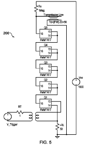
Fig. 5 shows a pulse generation circuit 200 that is an
embodiment of the invention. The pulse generation circuit 200
is similar to the circuit shown in Fig. 4, except that in
place of the single avalanche transistor, there is a plurality
30 (five in this example) of series-connected avalanche
transistors. The plurality of series-connected avalanche
transistors effectively operate in combination as a single
avalanche transistor. This means that the discharge of the
open-circuit transmission line is across the stacked
35 transistors to the load/ thereby resulting in a cascade effect
CA 03159846 2022-5-27
WO 2021/110605
PCT/EP2020/083975
11
that causes a proportionally higher pulse amplitude at the
load. In this example, each of the avalanche transistors is
identical so that the supply voltage Vcc is equally distributed
across each of the avalanche transistor in the series chain.
5 In this arrangement, the maximum pulse amplitude that can
be generated is dependent on the number of stacked avalanche
transistor n. The number of avalanche transistors required to
generate a specific pulse amplitude VI can be expressed as
10 VL = nBlIcRo ___________
(RLR-1-1.4)
where Blicfro is the collector-base breakdown voltage of
each avalanche transistor. If RL=20, a maximum pulse
amplitude Vranat can thus be expressed as
nAVC730
VLmax =
2
In the pulse generating circuit 200 five FMMT417
avalanche transistor are stacked. Each transistor has an
20 collector-emitter breakdown voltage BVcE0 of 100 V and a
collector-base breakdown voltage B17c60 of 320 V. The circuit
shown in Fig. 5 was simulated using LTSpice models. The Spice
model of the FMMT417 was directly taken from the manufacture's
website. The source resistance Re is 1 MD, characteristic
25 impedance of the transmission line 4 is 50 Q, source voltage
Vcc is 1.5kV.
The circuit may include a diode (not shown) connected in
parallel with each transistor to clamp the voltage to ensure
that the voltage across each transistor does not exceed its
30 collector-base breakdown voltage. Doing so can increase the
lifespan of the transistors and ensure that triggering occurs
by the trigger signal.
CA 03159846 2022-5-27
WO 20211110605
PCT/EP2020/083975
12
The trigger signal may be provided by any suitable
source. Preferably the trigger signal is generated by a TTL
source or a microcontroller. In this example, the trigger
signal comprises a pulse having a duration of 600 ns and a 5 V
5 amplitude and pulse period (period of repetition) of 20 ms.
It is advantageous to have a 5 V trigger signal because it is
less than the emitter-base breakdown voltage of the
transistors.
The pulse width of trigger signal is arranged to be
10 longer than the pulse desired to be generated from the
transmission line. The duration of 600 ns was chosen in this
case to provide a safe margin to allow the whole transmission
line to discharge.
The trigger signal repetition rate (pulse period) is
15 limited by the time it takes for the open-circuit charged
transmission line to charge up again to full capacity.
A transformer is disposed between the trigger signal
generator and the base and emitter of the first transistor in
the stack (i.e. the transistor furthest from the transmission
20 line). This configuration means that the trigger pulse is
floating, and therefore should be the same between the base
and emitter of the first transistor no matter the voltage
through the transistor and onto the load. As a result, the
amplitude of the pulse at the load ought to increase linearly
25 with the number of transistors in the stack. The transformer
may be a 1-EMR-046 Gate Drive Transformer having a 1:1 winding
ratio and high voltage isolation.
In use, the five stacked avalanche transistors are
initially in their off-state, with each transistor having 300
30 V across them (i.e. Vcc/n). When a positive trigger signal is
applied to the base of the first transistor Ql, Q1 is turned
Ion' and places its collector voltage near ground potential.
This results in the second transistor Q2 having twice the
collector-emitter voltage, thus creating the desired condition
35 in terms of overvolting and therefore causes a non-destructive
CA 03159846 2022-5-27
WO 20211110605
PCT/EP2020/083975
13
avalanching of Q2 and places its collector near ground
potential. This creates a sequential 'knock-on' effect on the
next transistor in the chain resulting in the overvolting of
the first avalanche transistors, Ql, to the final avalanche
5 transistors, Q5 near the charged open circuit transmission
line. When Q5 is turned 'on', a fast rise time is produced at
the load (< 2 ns), therefore allowing the charged open circuit
transmission line to discharge through the load producing a
pulse with a width of 2T and a maximum amplitude of 174x/2, if
10 RL=Zo.
The pulse generating circuit 200 may thus be used to
generate monopolar ultrashort electric field pulses.
Fig. 6 is a graph showing voltage pulses obtained for a
range of transmission line lengths. In Fig. 6, the
15 transmission line lengths are characterised by the line delay
T. The graph demonstrate that the transmission line length
determines the pulse width of 2T, i.e. transmission lines
having line delays of 5 ns, 25 ns, 50 ns and 100 ns produce
pulse widths of 10 ns, 50 ns, 100 ns and 200 ns respectively.
20 Additionally, the rise times of all four pulses are the same
and less than 2ns, which emphasises that the switching
element, i.e. the five avalanche transistors, determines this
factor.
The graph in Fig. 6 suggests that a 50 Q load does not
25 match the transmission line characteristic impedance because
secondary pulse of lower amplitude to the primary pulse is
seen on each signal. This suggested an unmatched load due to
reflection, i.e. r* o. The inventors have realised that it is
necessary to compensate for the impedance of the transistors
30 in order to optimise the pulse generation circuit. In the
example shown in Fig. 5, each individual transistor has an
impedance of -3 O. Therefore, a total of -15 C is across the
transistor stack. The reflection coefficient can thus be
expressed as
CA 03159846 2022-5-27
WO 2021/110605
PCT/EP2020/083975
14
r(RE ¨ Zo) ((Re + nRA) ¨ Zo)
¨ __________________________________________________________________
REA-zo (R,s+nRA)+Zo)
wherein the RE is the total impedance of the circuit, and
RA is the impedance of a signal avalanche transistor.
5 This explains the reflection observed in the pulses shown
in Fig. 6, as r = 0.13, and the amplitude of the reflection
pulse is -13% of the primary pulse (RL = 50 n, nRA = (3 0 x 5)
= 15 n and 4 = 50 0). The additional impedance of nRA also
affects the DC component of the design, which can be rewritten
10 as:
RL
VL =
_____________________________________________________________________________
Zo-FRA +RI) V`c
Taking this into account, the impedance of the load RL
was adjusted to 35 0. This resulted in a single monopolar
pulse at the load with zero reflection and no secondary pulse,
15 as shown in Fig. 7.
The circuit shown above in Figs. 4 and 5 is configured to
generate positive monopolar pulses. However, the circuit can
also be adapted to generate a negative monopolar pulse by
changing the position in which the load is connected. Fig. 8
20 is a schematic diagram of a pulse generating circuit 150 that
utilises an open circuit transmission line technique in
combination with an avalanche transistor as a fast switching
element similar to the circuit 100 in Fig. 4. The circuit 150
of Fig. 8 differs from the circuit of Fig. 4 in that the load
25 RL is connected so that current flows in the opposite direction
from Fig. 4 when the coaxial transmission line discharges.
Fig. 9 shows a pulse generation circuit 250 that is an
embodiment of the invention. The pulse generation circuit 250
is similar to the circuit shown in Fig. 5, except that the
30 load RL is connected so that current flows in the opposite
direction from Fig. 5 when the coaxial transmission line
discharges. Fig. 10 shows a graph of a negative monopolar
CA 03159846 2022-5-27
WO 2021/110605
PCT/EP2020/083975
pulse observed with a matched 35 Q load, obtained using the
circuit 250 shown in Fig. 9.
In a development of the concepts discussed above, the
pulse generating circuit can be configured as a bipolar pulse
5 generating circuit. The operation of such a circuit can be
identical to the monopolar designs in Figs. 4 and 9.
Fig. 11A is a schematic diagram of a pulse generation
circuit 300 that is an embodiment of a bipolar pulse
generating circuit 300. It is similar to the circuits shown in
10 Figs. 4 and 9, except that the pulse is generated on two
separate loads, which are marked at RL+ and RL_ in Fig. 11A.
These load location correspond to the locations for the
positive and negative pulses discussed above.
The bipolar pulse generating circuit 300 produces a
15 bipolar pulse, as the voltage difference across RL+ produces a
positive pulse, where the voltage difference across
produces a negative pulse. When the circuit 300 is used,
these pulses observed at on RL+ and Rit_ simultaneously and are
symmetrical, i.e. with the same pulse width, rise time,
20 amplitude a repletion rate, but of different polarity.
As there are two loads in this circuit, the optimisation
equations to reduce reflection must be revised. For a bipolar
design the total load impedance, REL = RL++RL_I is the
impedance between the transmission line's outer conductor and
25 the emitter of avalanche transistor 01 and is the sum
impedance of RL+ and The
reflection coefficient can
therefore be expressed using transmission line theory as:
r_ RREL + nRA) -Z0\)
+ RL+ -FrtRA)- Z0A
(REL +nRA)+ Zo
+ RL+ nRA) + Zo)
r = o
Similarly, the peak-to-peak voltage VEL over the loads can
be expressed using DC theory as:
CA 03159846 2022-5-27
WO 2021/110605
PCT/EP2020/083975
16
REL
VEL = VL+ VL_ =
_____________________________________________________________________________
Vcc
(Z0 + RA + I?)
VL_
_______________________________________________________________________________
20 + RA + REL)V
cc
RL+
VL+ Vcc
Z0 + RA + EEL'
wherein VL+ and Kr are the amplitudes of the positive and
negative pulses respectively.
From the above, RL+ and RL_ values of 17.5 0 would produce
a bipolar pulse of a single pulse with zero reflection (I' = 0),
and a simultaneous symmetrical pulse width of 2T and rise
times < 2ns. Put another way, the bipolar pulse generating
circuit 300 operates to create a single positive pulse of
amplitude VEL between the transmission line's outer conductor
and the emitter of avalanche transistor Ql, across REL with a
pulse width of 2T and zero reflection.
Fig. 12A is a graph that shows a pulse 310 observed at
RL+, a pulse 312 observed at RL_, and a pulse 314 observed at
REL. These observations verify the theory presented above. In
Fig. 12A, a 5ns transmission line produces a lOns pulse at all
three loads with identical rise times (<2ns). As RL+ = RL_ =
17.5 Q, there is no reflection, i.e.
rCRL_+RL+ nRA) - Zo)
(07.5 + 17.5 -I- 15) - 50)
= =0
(R L_ RL+ nRA) Z0
(17.5 17.5 -I- 15) -I- 50
The magnitude of VL+ and VL_ is 262.5 V, so the peak-to-
peak voltage VEL is 520 V, which is the same as the equivalent
monopolar design.
Fig. 116 is a schematic diagram of a bipolar pulse
generation circuit 350 that is another embodiment of the
CA 03159846 2022-5-27
WO 2021/110605
PCT/EP2020/083975
17
invention. The circuit in Fig. 11B differs from Fig. 11A by
providing a delay line before each of the loads (RL+ and RL_).
Placing a delay line before one or both loads allows
manipulation of a delay between the two pulses. A delayed
5 pulse will follow a non-delayed paired pulse by the delay time
minus pulse width. In Fig. 118, a 20 ns delay line is placed
before kr__
Fig. 126 is a graph similar to Fig. 12A that shows a
pulse 310 observed at RL+, a pulse 312 observed at RL_, and a
10 pulse 314 observed at REL. Fig. 128 confirms the effect of the
introducing the delay line, as all the three pulses in Fig.
128 and there parameters are identical to the Fig. 12A. The
only difference is that the negative pulse across RL_ follows
the positive pulse by lOns (i.e. 20ns - 10 ns).
15 The bipolar pulse generation circuit configuration
discussed herein is thus capable of producing:
- a symmetrical bipolar pulse, with positive and negative
parts generated simultaneously or sequentially (i.e. with
differing delays)
20 - zero reflection but adjustable VL+ and VL_ amplitudes,
because the amplitudes are controlled by the ratio of RIA and
Rir but the reflection will remain zero if REL =RL,_-ERL+ =Z0¨
nki condition is met.
In a further development, one or both of the delay lines
25 may have an adjustable length that allows the introduced delay
to be controlled. This may permit the separation of the
positive and negative pulses to be adjusted on the fly, e.g.
so that the instrument is capable of generating a variety of
electroporation waveforms.
REFERENCES
[1] W. Meiling and F. Stary, Nanosecond pulse
techniques. New York: Gordon and Breach, 1970, p. 304.
CA 03159846 2022-5-27
WO 2021/110605
PCT/EP2020/083975
18
[2] Q. Yang, X. Zhou, Q.-g. Wang and M. Zhao,
"Comparative analysis on the fast rising edge pulse source
with two kinds of avalanche transistor," in Cross Strait Quad-
Regional Radio Science and Wireless Technology Conference,
Chengdu, 2013.
[3] G. Yong-sheng et al., "High-speed, high-voltage
pulse generation using avalanche transistor," Review of
Scientific Instruments, vol. 87, no. 5, p. 054708, 2016.
CA 03159846 2022-5-27