Note: Descriptions are shown in the official language in which they were submitted.
WO 2021/138494
PCT/US2020/067570
SATELLITE FORWARD LINK NON-LINEAR NOISE AND APSK I/Q IMBALANCE ERROR
CANCELLATION USING ARTIFICIAL INTELLIGENCE
CROSS-REFERENCE TO RELATED APPLICATION
100011 This application claims priority to U.S. Application No.
16/730,692 (filed December
30, 20119), the entire disclosure of which is incorporated herein by
reference.
BACKGROUND INFORMATION
100021 Modern communication technologies have enabled delivery of multimedia
services (e.g.,
voice, data, video, etc.) to end-users over various delivery platforms,
including terrestrial wire-
line, fiber and wireless communications and networking technologies, and
satellite
communications and networking technologies. The relatively recent
proliferation of mobile
communications has spurred growth in the demand for such enhanced multimedia
services over
fixed and mobile communications networks (both terrestrial and satellite
based). Developments
in both fixed and mobile wireless communications have enabled consumers to
remain connected
without the need to have a wired connection. For example, satellite
communication systems
allow consumers to access voice and data services from virtually any global
location. Such
accessibility can be beneficial for consumers who are located in, or must
travel to, areas that
cannot be serviced by other (e.g. terrestrial) communication systems. As part
of the growing
demand, service providers of voice and communication networks are faced with
requests for
seemingly endless levels of bandwidth by consumers and content providers.
Consumers utilize
devices such as mobile phones, tablets, computers, etc. to obtain various
types of content which
CA 03161214 2022- 6-8
WO 2021/138494
PCT/US2020/067570
can often require greater bandwidth and a higher quality of service than
required only a short
period of time earlier.
100031 To address the growing demand, several standards organizations have
enacted
specifications associated with the transmission and reception of fixed and
mobile wireless signal.
One such standard, the Digital Video Broadcasting (DVB) standard DVB-S2 is a
digital satellite
transmission system standard covering a variety of data and multimedia
services delivered over
satellite communications systems. The DVB-S2 standard also covers various
technological
features including a flexible input stream adapter that can utilize Adaptive
Coding and
Modulation (ACM) functionality for optimizing channel coding and modulation on
a frame-by-
frame basis. The transmission equipment and transmission channel environment
associated with
satellite signals can introduce signal impairment that remain in the signal
when received at user
terminals. These impairments in the received signal place a performance strain
on signal
receiving circuit in user terminals, particularly when receiving signals
adhering to the DVB-S2
standard.
100041 Typically, several signal demodulation support circuits are employed to
mitigate or
remove these impairments. The signal demodulation support circuits can have
shortcomings,
including, but not limited to, constraints on types or areas of impairments
that can be processed
and time response limiting control or feedback loops. Further, the signal
demodulation circuits
often operated independently, limiting collective mitigation capability. These
shortcomings can
limit the data throughput or data rate for the signal and restrict the range
of possible modulation
type or forward error corrections that can be used when encoding the signal
for transmission.
Based on the foregoing, there is a need to improve the performance of the
signal receiver in
2
CA 03161214 2022- 6-8
WO 2021/138494
PCT/US2020/067570
terminals (such as satellite terminals) and, in particular, the impairment
mitigation performance
of the demodulator in the receiver.
3
CA 03161214 2022- 6-8
WO 2021/138494
PCT/US2020/067570
BRIEF SUMMARY
[0005] A method and apparatus are disclosed for non-linear noise cancelation
and in phase
quadrature (I/Q) modulation error correction. According to an embodiment, the
method
includes: receiving a signal, the signal including a plurality of data
segments; demodulating a
first data segment in the received signal; decoding the demodulated first data
segment to produce
a recovered segment of a bitstream; and applying at least one correction
factor to a first
demodulation support element and a second demodulation support element during
demodulation
of a second data segment in the received signal, the at least one correction
factor being based on
the received first data segment and a representation of the first data segment
reconstructed from
the recovered segment of the bitstream.
[0006] According to an embodiment, the apparatus includes: an input circuit
that receives a
signal, the signal including a plurality of data segments; a demodulator
coupled to the receiving
circuit, the demodulator demodulating a first data segment in the received
signal; a decoder
coupled to the demodulator, the decoder decoding the demodulated first segment
to produce a
recovered segment of a bitstream; and an error cancellation module coupled to
the demodulator
and the decoder, the error cancellation module applying at least one
correction factor to a first
demodulation support element and a second demodulation support element during
demodulation
of a second segment of the signal, the correction factor being based on the
received first data
segment and a representation of the first data segment reconstructed from the
recovered segment
of the bitstream.
4
CA 03161214 2022- 6-8
WO 2021/138494
PCT/US2020/067570
100071 The foregoing summary is only intended to provide a brief introduction
to selected
features that are described in greater detail below in the detailed
description. As such, this
summary is not intended to identify, represent, or highlight features believed
to be key or
essential to the claimed subject matter. Furthermore, this summary is not
intended to be used as
an aid in determining the scope of the claimed subject matter.
CA 03161214 2022- 6-8
WO 2021/138494
PCT/US2020/067570
BRIEF DESCRIPTION OF THE DRAWINGS
[0008] Various exemplary embodiments are illustrated by way of example, and
not by way of
limitation, in the figures of the accompanying drawings in which like
reference numerals refer to
similar elements and in which:
[0009] Fig. 1 is a diagram of a system capable of providing voice and data
services, according to
at least one embodiment;
100101 Fig. 2 is a diagram of a terminal such as used in the system of Fig. 1,
according to one
embodiment;
[0011] Fig. 2 is a diagram of a transmitter such as used in the terminal of
Fig. 2, according to one
embodiment;
[0012] Fig. 4 is a diagram of a receiver such as used in the terminal of Fig.
2, according to one
embodiment;
[0013] Fig. 5 is a flowchart of a process for demodulating and decoding a
received signal,
according to one embodiment;
[0014] Fig. 6A and Fig. 6B is a flowchart of a process for generating a set of
correction factors,
according to at least one embodiment;
[0015] Fig. 6B is a flowchart of a process for generating a set of correction
factors, according to
at least one embodiment;
[0016] Fig. 7 is a diagram of a constellation map for a received signal,
according to one or more
embodiments;
6
CA 03161214 2022- 6-8
WO 2021/138494
PCT/US2020/067570
100171 Fig. 8 is a diagram of another constellation map for a received signal,
according to one or
more embodiments;
100181 Fig. 9 is a diagram of a computer system that can be used to implement
various
exemplary features and embodiments; and
100191 Fig. 10 is a diagram of a chip set that can be used to implement
various exemplary
features and embodiments.
7
CA 03161214 2022- 6-8
WO 2021/138494
PCT/US2020/067570
DETAILED DESCRIPTION
[0020] A method and apparatus for demodulating and decoding a received signal
capable of
improving data throughput for devices such as a terminal are described. In the
following
description, for purposes of explanation, numerous specific details are set
forth in order to
provide a thorough understanding of the disclosed embodiments. It will become
apparent,
however, to one skilled in the art that various embodiments may be practiced
without these
specific details or with an equivalent arrangement. In other instances, well-
known structures and
devices are shown in block diagram form in order to avoid unnecessarily
obscuring the various
embodiments.
[0021] The present embodiments are directed to improving bandwidth efficiency
(e.g., data
throughput, quality of service, etc.) in a terminal of a wireless
communication network, such as a
satellite communication network. The embodiments apply correction factors to
demodulation
support elements during demodulation of data segments or symbols in a received
signal at the
terminal. These demodulation support elements can include an I/Q balance
element, a
synchronization element, a linear equalization element a non-linear
equalization element, and the
like. These elements are included for mitigating the presence of signal
impairments such as
additional noise, distortion, and/or interference introduced through the
equipment used for
transmitting the signal as well as the transmission channel through which the
signal passes.
[0022] The mechanism described by the present embodiments analyzes the
relation between the
input data received in the signal and error correction decoder output data for
every data segment,
or symbol, in real time or using data stored in memory to make segment-based
(or symbol-based)
8
CA 03161214 2022- 6-8
WO 2021/138494
PCT/US2020/067570
noise and error correction equations and correction factors that are used to
control or adjust the
demodulator data recovery for the next data segment or symbol. The processing
can be
performed using the real time data or can include all or portions of data that
are stored in
memory. In some embodiments, the mechanism can include deep learning functions
associated,
for example, with artificial intelligence (AI) operations. The mechanism can
enhance noise,
distortion, and/or interference cancellation along with forward error
correction capability as part
of recovering signals that include noise, distortion, and/or interference from
impairments that
may not otherwise be mitigated or eliminated. In some embodiments, such as
user terminals that
employ ACM as part of DVB-S2 signal transmission, the mechanism can be used to
increase
forward communication (e.g., satellite communication) link speed and data or
bandwidth
efficiency. For instance, the user terminal can send a request back through
the communication
network to provide subsequent data segments encoded with a different, less
robust set of transmit
parameters as part of the transmitted signal. This different set of transmit
parameters can be less
robust than the set of transmit parameters that would be used if no correction
factors were
applied
100231 Fig. 1 illustrates a satellite communication system 100 capable of
providing voice and
data services. The satellite communication system 100 includes a satellite 110
that supports
communications among a number of gateways 120 (only one shown) and multiple
stationary
satellite terminals 140a-140n. Each satellite terminal (or terminal) 140 can
be configured for
relaying traffic between its customer premise equipment (CPEs) 142a-142n
(i.e., user
equipment), a public network 150, such as the interne, and/or its private
network 160.
Depending on the specific embodiment, the CPEs 142 can be a desktop computer,
laptop, tablet,
9
CA 03161214 2022- 6-8
WO 2021/138494
PCT/US2020/067570
cell phone, etc. CPEs 142 can also be in the form of connected appliances that
incorporate
embedded circuitry for network communication can also be supported by the
satellite terminal
(or terminal) 140. Connected appliances can include, without limitation,
televisions, home
assistants, thermostats, refrigerators, ovens, etc. The network of such
devices is commonly
referred to as the internet of things (IoT).
100241 According to an exemplary embodiment, the terminals 140 can be in the
form of very
small aperture terminals (VSATs) that are mounted on a structure, habitat,
etc. Depending on the
specific application, however, the terminal 140 can incorporate an antenna
dish of different sizes
(e.g., small, medium, large, etc.). The terminals 140 typically remain in the
same location once
mounted, unless otherwise removed from the mounting. According to various
embodiments, the
terminals 140 can be mounted on mobile platforms that facilitate
transportation thereof from one
location to another. Such mobile platforms can include, for example, cars,
buses, boats, planes,
etc. The terminals 140 can further be in the form of transportable terminals
capable of being
transported from one location to another. Such transportable terminals are
operational only after
arriving at a particular destination, and not while being transported.
100251 As illustrated in Fig. 1, the satellite communication system 100 can
also include a
plurality of mobile terminals 145 that are capable of being transported to
different locations by a
user. In contrast to transportable terminals, the mobile terminals 145 remain
operational while
users travel from one location to another. The terms user terminal, satellite
terminal, terminal
may be used interchangeably herein to identify any of the foregoing types. The
gateway 120 can
be configured to route traffic from stationary, transportable, and mobile
terminals (collectively
terminals 140) across the public network 150 and private network 160 as
appropriate. The
CA 03161214 2022- 6-8
WO 2021/138494
PCT/US2020/067570
gateway 120 can be further configured to route traffic from the public network
150 and private
network 160 across the satellite link to the appropriate terminal 140. The
terminal 140 then
routes the traffic to the appropriate CPE 142.
100261 According to at least one embodiment, the gateway 120 can include
various components,
implemented in hardware, software, or a combination thereof, to facilitate
communication
between the terminals 140 and external networks 150, 160 via the satellite
110. According to an
embodiment, the gateway 120 can include a radio frequency transceiver (RFT)
122, a processing
unit 124 (or computer, central processing unit (CPU), etc.), and a data
storage unit 126 (or
storage unit). While generically illustrated, the processing unit 124 can
encompass various
configurations including, without limitations, a personal computer, laptop,
server, etc. As used
herein, a transceiver corresponds to any type of antenna unit used to transmit
and receive signals,
a transmitter, a receiver, etc. The RFT 122 is useable to transmit and receive
signals within a
communication system such as the satellite communication system 100
illustrated in Fig. 1. The
data storage unit 126 can be used, for example, to store and provide access to
information
pertaining to various operations in the satellite communication system 100.
Depending on the
specific implementation, the data storage unit 126 (or storage unit) can be
configured as a single
drive, multiple drives, an array of drives configured to operate as a single
drive, etc.
100271 According to other embodiments, the gateway 120 can include multiple
processing units
124 and multiple data storage units 126 in order to accommodate the needs of a
particular system
implementation. Although not illustrated in Fig 1, the gateway 120 can also
include one or
more workstations 125 (e.g., computers, laptops, etc.) in place of, or in
addition to, the one or
more processing units 124. Various embodiments further provide for redundant
paths for
11
CA 03161214 2022- 6-8
WO 2021/138494
PCT/US2020/067570
components of the gateway 120. The redundant paths can be associated with
backup
components capable of being seamlessly or quickly switched in the event of a
failure or critical
fault of the primary component.
100281 According to the illustrated embodiment, the gateway 120 includes
baseband components
128 which operate to process signals being transmitted to, and received from,
the satellite 110.
For example, the baseband components 128 can incorporate one or more
modulator/demodulator
units, system timing equipment, switching devices, etc. The
modulator/demodulator units can be
used to generate carriers that are transmitted into each spot beam and to
process signals received
from the terminals 140. The system timing equipment can be used to distribute
timing
information for synchronizing transmissions from the terminals 140.
100291 According to an embodiment, a fault management unit 130 can be included
in the
gateway 120 to monitor activities and output one or more alerts in the event
of a malfunction in
any of the gateway components. The fault management unit 130 can include, for
example, one
or more sensors and interfaces that connect to different components of the
gateway 120. The
fault management unit 130 can also be configured to output alerts based on
instructions received
from a remotely located network management system 170 (NMS). The NMS 170
maintains, in
part, information (configuration, processing, management, etc.) for the
gateway 120, and all
terminals 140 and beams supported by the gateway 120. the gateway 120 can
further include a
network interface 132, such as one or more edge routers, for establishing
connections with a
terrestrial connection point 134 from a service provider.
Depending on the specific
implementation, however, multiple terrestrial connection points 134 may be
utilized.
12
CA 03161214 2022- 6-8
WO 2021/138494
PCT/US2020/067570
[0030] Fig. 2 is a diagram of an exemplary configuration for a terminal 200
capable of
implementing signal reception improvements, according to one embodiment.
Depending on the
specific implementation, terminal 200 can be configured to operate as a fixed
satellite terminal
140 (e.g., VSAT), a mobile terminal 145, a transportable terminal, etc. In
terminal 200, a CPU
210 is coupled to a storage unit 220, a memory 230, a local network interface
240, a user
interface 250, and a modem 260. Modem 260 is further coupled to a transmit
radio frequency
(RF) unit 270 and a receive RF unit 280. Although not shown, power supply 290
can be coupled
to each of the blocks shown in terminal 200 that require local electrical
power. It should be
noted that terminal 200 can include various additional components which
perform conventional
operations. Such components are well known to those skilled in the art and are
omitted in order
to provide better clarity and conciseness in describing the novel features of
terminal 200.
[0031] CPU 210 can include one or more specifically built processing elements
and/or general
purpose processors configured or programmed to perform specific tasks
associated with the
operation, control, and management of activity in terminal 200. Storage unit
220 can be any one
of several large and/or removable storage elements including, but not limited
to, magnetic disk,
and optical disk. Memory 230 can be any type of electronic circuit or small
scale based storage
elements including, but not limited to read-only memory (ROM), erasable
electrically
programmable ROM (EEPROM), random-access memory (RAM), non-volatile RAM
(NVRAM), flash memory, or other similar memory technology. Storage unit 220
and/or
memory 230 can be used to store instructions or software code used by CPU 210
and data
associated with operation of terminal 200. Storage unit 220 can also be used
for longer term
storage of data and/or multimedia content transmitted and/or received through
modem 260 or
13
CA 03161214 2022- 6-8
WO 2021/138494
PCT/US2020/067570
local network interface 240. Memory unit 230 can be used for shorter term or
temporary storage
of data and/or multimedia content needed for, or associated with, signal and
data processing in
terminal 200.
100321 Local network interface 240 includes circuit elements configured for
interfacing to one or
more home networks and/or other similar local area networks (LANs). Local
network interface
240 also includes interface components for connecting to the home networks
and/or LANS either
through a wired medium or wirelessly. Local network interface 240 receives
data and/or
multimedia content, along with processing instructions, from CPU 210 for
delivery to devices
such as CPEs 142 on the home and/or local area networks. For example, a CPE
142 such as a
home computer in a user's local home network employing Ethernet protocols can
be interfaced
to local network interface 240 through a registered jack (RJ) type 45
receptacle using category 5
(CAT 5) cable or later variants (e.g. CAT 6, CAT 7, etc.). Further, a CPE such
as a user's cell
phone can be connected wirelessly to local network interface 240 through an
antenna (not
shown) in order to utilize terminal 200 as a Wi-Fi signal router, repeater, or
hotspot.
100331 User interface 250 can include a user input or entry mechanism, such as
a set of buttons
on an infrared/RF/Bluetooth remote controller, a keyboard, or a microphone.
User interface 250
can also include circuitry for converting user input signals into a data
communication format to
provide to processor 210. User interface 250 can further include some form of
user notification
mechanism to show device functionality or status, such as indicator lights, a
speaker, or a
display. User interface 250 can also include circuitry for converting data
received from
processor 210 to signals that may be used with the user notification
mechanism.
14
CA 03161214 2022- 6-8
WO 2021/138494
PCT/US2020/067570
[0034] Modem 260 performs functions necessary for modulating and demodulating
a signal
to/from transmit RF unit 270 and receive RF unit 280. These elements and/or
functions can
include, but are not limited to, digital signal conditioning, symbol mapping,
demapping, data
error correction encoding/decoding, and transport stream processing for
interfacing data to and
from the CPU 210. According to various embodiments, modem 260 can perform the
modulating/demodulating functions independently or under control of the CPU
210. Transmit
RF unit 270 processes the digital signal from modem 260 to form an analog
signal for
transmission through a satellite dish included as part of an outdoor unit
(ODU) or an antenna (not
shown). Receive RF unit 280 processes the analog signal received through the
satellite dish or
antenna to form a digital signal that is further processed in modem 260. the
processing elements
or functions in transmit RF unit 270 and receive RF unit 280 include, but are
not limited to,
signal amplification, filtering frequency up/downconversion, and analog to
digital signal or
digital to analog signal conversion.
[0035] In one embodiment, the received satellite signal, operating in the Ka
or Ku frequency
bands, is first block downconverted to the L band frequency range using very
high frequency
components in the ODU (not shown). The received satellite signal can be
encoded using one or
more sets of transmit parameters, including a set of transmit parameters
associated with terminal
200. The downconverted received signal in the L band frequency range is
provided to receive
RF unit 280, where it is processed to provide a digital signal representing
the received signal.
Modem 260 processes the digital signal to produce a transport stream
containing data that is
associated with or, for delivery to, one or more user devices on a local area
network. Modem
260 can further apply additional processing, such as deep learning functions,
to generate
CA 03161214 2022- 6-8
WO 2021/138494
PCT/US2020/067570
additional correction factors for use in demodulating signals received at
satellite terminal 200
For example, the additional processing can include generating correction
factors to mitigate or
remove the presence of undesired signal energy, such as I/Q balance errors,
synchronization
mistracking, and signal non-linearities or distortion, in the received signal
during demodulation.
The data recovered from the received signal is processed in CPU 210 and
provided to local
network interface 240 for delivery to the one or more devices.
100361 Further, data from the one or more devices is provided to CPU 210
through local network
interface. CPU 210 processes the data to form a transport stream and provides
the transport
stream to modem 260. CPU 210 can also generate messages for the satellite
gateway and add
them to the transport stream. Such messages can include, for example, requests
to change the set
of transmit parameters associated with terminal 200, system messages, status
reports, etc.
Modem 260 processes the transport stream to produce a digital signal
representing a signal for
transmission as a satellite signal. The digital signal is provided to transmit
RF unit 270, which
processes the digital signal to form an analog signal in the L band frequency
range. Transmit RF
unit 270 provides the L band signal to the ODU for block upconversion and
transmission as a
satellite signal in the KA or Ku frequency bands. While Fig. 2 illustrates
components such as
modem 260, transmit RF unit 270, and receive RF unit 280, within terminal 200,
it should be
noted that various embodiments can allow for part or all of one or more of
these components to
be included in the ODU. Further, parts of one or more components may be
combined or
rearranged without altering the overall function and purpose of terminal 200.
Thus, the specific
arrangement shown in Fig. 2 should only be considered as illustrative and is
in no way intended
to be restrictive.
16
CA 03161214 2022- 6-8
WO 2021/138494
PCT/US2020/067570
100371 Fig. 3 is a diagram of an exemplary transmitter 300 that can be
configured to operate as
part of the terminal in Fig. 2, in accordance with one embodiment. In
transmitter 300, data block
310 provides an interface for the received transport stream. Data block 310 is
coupled to BCH
encoder 320. BCH encoder 320 is coupled to Low Density Parity Check (LDPC)
encoder 330.
LDPC encoder 330 is coupled to bit interleaver 340. Bit interleaver 340 is
coupled to symbol
modulator 350. Symbol modulator 350 is coupled to digital-to-analog converter
(DAC) 360.
DAC 360 is coupled to RF processor 370, which provides a signal to an ODU such
as an RF
transmitter.
100381 Data block 310 receives the transport stream data and performs layer
encapsulation to
form baseband data frames or data blocks. Data block 310 can also insert
information associated
with processing of the signal, such as terminal identification information
and/or one or more
transmit parameters used for processing and/or encoding portions of the
signal. BCH encoder
320 processes the baseband data frames by adding additional redundant
information based on
one or more of the BCH encoding algorithms used in conjunction with the signal
transmission
protocol. The additional redundant information, referred to as error
correction information, can
be used for correction of errors introduced by the transmission of the signal
over the transmission
channel or link during signal reception. LDPC encoder 330 further processes
the BCH encoded
data frames to add a second layer of redundant information, or error
correction information, to
the data frames for error correction using one or more LDPC algorithms. Bit
interleaver 340
processes the data frames including the two layers of error correction to
rearrange sections (e.g.,
bits) of the data frames with respect to location or position (i.e., in time)
within the data frames
to provide some additional error correction capability during reception to due
short term signal
17
CA 03161214 2022- 6-8
WO 2021/138494
PCT/US2020/067570
interference events. Symbol modulator 350 arranges the bits within the frames
into symbols
representing positions (i.e., in amplitude, phase, and/or time) in a modulated
signal waveform
based a symbol constellation map for the modulation type. DAC 360 converts the
digital signal,
arranged into symbols, to an analog signal, typically at or near the baseband
frequency range.
RF processor 370 filter, amplifies and upconverts the analog signal to produce
a signal in the L
band frequency range and provide the signal to an ODU for transmission.
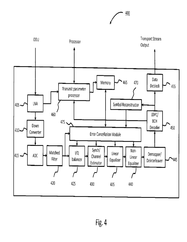
100391 Fig. 4 is a diagram of an exemplary receiver 400 that can be configured
to operate as part
of the terminal in Fig. 2, in accordance with one embodiment. In receiver 400,
the satellite
signal received by the ODU is provided as an input to low noise amplifier
(LNA) 405. LNA 405
is coupled to downconverter 410. Downconverter 410 is coupled to analog-to-
digital converter
(ADC) 415. ADC 415 is coupled to matched filter 420. Matched filter 420 is
coupled to I/Q
balancer 425. I/Q balancer 425 is coupled to synchronization (synch)/channel
estimator 430.
Synch/channel estimator 430 is coupled to linear equalizer 435. Linear
equalizer 435 is coupled
to non-linear equalizer 440. Non-linear equalizer 440 is coupled to
demapper/deinterleaver 445.
Demapper/deinterleaver 445 is coupled to LDPC/BCH decoder 450. LDPC/BCH
decoder 450 is
coupled to data deblock 455 which provides a transport stream output signal.
LDPC/BCH
decoder 450 is also coupled to symbol reconstructor 470. Both symbol
reconstructor 470 and
matched filter 420 are coupled to error cancellation module 475. Error
cancellation module 475
is coupled to I/Q balancer 425, synch/channel estimator 430, and linear
equalizer 435. Although
not shown in Fig. 4, the error cancellation module 475 is also coupled to
memory 465 in order to
store and retrieve information while processing the received satellite signal.
Further, transmit
parameter processor 460 is coupled to LNA 405 and LDPC/BCH decoder 450 as well
as memory
18
CA 03161214 2022- 6-8
WO 2021/138494
PCT/US2020/067570
465. Transmit parameter processor 460 can also include an interface to a
processor in the
terminal (e.g., CPU 210 as part of terminal 200 in Fig. 2).
100401 LNA 405 receives the received signal in the L band frequency range, and
filters and
amplifies the signal to remove other signal energy not within the frequency
range of a desired
portion of the signal. Depending on the specific implementation, the received
signal in the L
band frequency range can contain a plurality of individual signals arranged
into channels or
transponders. Downconverter 410 frequency converts the filtered signal,
referred to as the
desired signal (e.g., a channel or transponder), to a frequency range at or
near the baseband
frequency range. Downconverter 410 can also provide additional filtering, if
necessary.
Typically, not all of the plurality of individual signals contain data
associated with, or intended
for use by, the terminal that includes receiver 400. Data in the signal that
is associated with, or
intended for use by, the terminal can be based on requests made through user
devices (e.g. CPEs
142 in Fig. 1) connected to terminal 200 (e.g., through local network
interface 240 in Fig. 2),
referred to as desired data in the desired signal. ADC 415 converts the
downconverted signal to
a digital signal representative of the downconverted signal. In some
embodiments, more than
one LNA 405, downconverter 410, and ADC 415, referred to collectively as a
desired signal
tuner, can be included for receiving and tuning a plurality of desired signals
from the received
signal.
100411 Matched filter 420 provides a defined filtering characteristic in order
to properly shape
the time domain representation of the symbols in the digital signal. I/Q
balancer 425 adjusts the
relative position of the recovered symbols amplitude, phase, and/or time based
on an expected
position of the symbols within a defined constellation map for encoding the
modulation type in
19
CA 03161214 2022- 6-8
WO 2021/138494
PCT/US2020/067570
the received signal. Synch/channel estimator 430 detects specific portions of
the digital signal to
perform symbol timing synchronization and determine one or more of the
transmit parameters
used as part of encoding the transmitted signal. In some cases,
synchronization information as
well as transmit parameter information can be included in a specific portion
of the signal such as
part of a preamble or signal header.
100421 Synch/channel estimator 430 also processes the digital signal to
generate and maintain a
continuous updated estimate of the amplitude and phase response of the digital
signal as
compared to a perfect, ideal, or expected received signal. Transmission of the
signal from a
satellite gateway uplink (e.g., RFT 122 included in gateway 120 in Fig. 1) up
to a satellite (e.g.,
satellite 110) and back to the terminal can introduce a number of signal
impairments that may
additionally vary in time, including, but not limited to, nonstochastic noise,
signal reflections and
echoes, non-linear signal attenuation, etc. The estimate generated by
synch/channel estimator
430 allows receiver 400 to compensate, correct, and/or mitigate the effects of
the impairments
introduced into the signal. The estimate can be generated and maintained in
one or both of the
time domain and the frequency domain.
100431 Linear equalizer 435 corrects, to the extent possible, the presence of
impairments in the
digital signal based on the estimate provided from synch/channel estimator
430. Linear equalizer
435 processes the digital signal using a linear combination of scaled and
delayed versions of the
input digital to attempt to invert or cancel the presence of the impairment
from the digital signal,
often referred to as equalization. Non-linear equalizer 440 further corrects,
to the extent
possible, any remaining impairment errors still present in the digital signal
after equalization in
linear equalizer 435. Non-linear equalizer 440 corrects for those errors that
cannot be addressed
CA 03161214 2022- 6-8
WO 2021/138494
PCT/US2020/067570
through only corrections of amplitude and/or phase performed in linear
equalizer 435 without
introducing an instability to the output response. Non-linear equalizer 440
can include additional
feedback and feedforward conditional decision loops in order to ensure
stability in the response
while correcting for the effects or presence of the remaining portion of
impairments in the digital
signal. The I/Q balancer 425, synch/channel estimator 430, and linear
equalizer 435 can be
referred to as demodulation support elements that can collectively make up a
circuit referred to
as a demodulator. Each of these demodulation support elements can operate on
specific effects
and/or errors that are present in the received signal and introduced as a
result of impairments
during signal transmission. In some embodiments, more or fewer, as well as
different
demodulation support elements can be used based on the requirements of
operation for the
receiver.
[0044] Demapper/deinterleaver 445 demodulates the digital signal waveform by
demapping the
symbols into strings of bits. Demapper/deinterleaver 445 further deinterleaves
the bits,
rearranging bits with respect to position or location in a manner that
reverses the interleaving
process applied at the transmitter (e.g., in bit interleaver 340 in Fig. 3).
LDPC/BCH decoder 450
processes the deinterleaved bitstream by first processing the redundant
information inserted by
the LDPC encoding process to identify and correct any correctable errors in
the bitstream, and
then processing the redundant information inserted by the BCH encoding process
to identify and
correct any additional correctable errors in the bitstream. Depending on the
amount or rate of
error correction applied as part of BCH and LDPC encoding, not all errors
present in the
bitstream can be identified and/or corrected by LDPC/BCH encoder 450. Data
deblock 455
processes the decoded bitstream (with or without remaining errors), arranged
in data blocks, to
21
CA 03161214 2022- 6-8
WO 2021/138494
PCT/US2020/067570
regenerate an estimate of the original source data as part of a transport
stream Data deblock 455
provides the transport stream to a processor, such as CPU 210 described in
Fig. 2, for further
processing and distribution. The transport stream includes desired data
intended for, or
associated with, the terminal and/or user devices interfaced to the terminal.
In addition, the
transport stream can also include data that is not destined for, or associated
with, the terminal
and/or user devices. Other processing, either in receiver 400 or in other
elements of the terminal,
can identify, parse, and/or discriminate the desired data from the undesired
data in the transport
stream.
100451 LNA 405 can perform further processing to determine signal energy or
level as well as
noise energy or level. The determined values for signal energy and noise
energy can be
processed to generate signal characteristics for the received signal. LDPC/BCH
decoder 450 can
also provide datastream characterization information associated with the error
correction process
as part of decoding the received digital bitstream. The signal characteristics
from LNA 405 as
well as the datastream characterization information from LDPC/BCH decoder 450
can be used
during ACM operation for signals transmitted using the DVB-S2 standard.
Transmit parameter
processor 460 can process the signal characteristics and/ or datastream
characterization as part of
determining a set of transmit parameters that can be used for transmitting
future data as part of a
desired signal intended for reception in receiver 400 as part of a user
terminal (e.g., terminal 200
in Fig. 2). Memory 465 can store any intermediate values as part of the
processing and
determination performed in transmit parameter processor 460. Memory 465 can
also store any
mapping that is created or defined based on a relationship between the
transmit parameters as
22
CA 03161214 2022- 6-8
WO 2021/138494
PCT/US2020/067570
part of ACM, and any characterization information provided by LNA 405 and
LDPC/BCH
decoder 450.
100461 Error cancellation module 470 receives the digitized and filtered input
signal from
matched filter 420 as a digital signal that represents the same digitized and
filtered input signal
after the input signal has been demodulated and decoded. The representative
input signal is
generated by providing the decoded bitstream from LDPC/BCH decoder 450 to
symbol
reconstructor 470. Symbol reconstructor 470 generates the representative
signal, which can be
referred to as a virtual or ideal input signal, by re-encoding the decoded
bitstream using the same
coding rate, re-interleaving the re-encoded bitstream using the same
interleaving rate, and re-
mapping the re-interleaved bitstream into symbols using the same mapping
process applied to
the originally transmitted signal. It is noted that symbol reconstructor 470
reverses a portion of
the demodulation and decoding processing that was applied to the input signal
in receiver 400.
However, because data errors that were introduced due to signal impairments
during
transmission of the signal have been corrected or removed by LDPC/BCH decoder
450, the
representative signal appears to be the same as the signal prior to its
transmission by the gateway
(e.g., satellite gateway 120 in Fig. 1).
100471 Error cancellation module 470 generates a comparison of a data segment
in the input
signal from matched filter 420 and the same data segment in the representative
input signal from
symbol reconstructor 470 based on one or comparison functions or equations. A
data segment
can be a predefined size, such as a data block, or may be a variable size
depending on
modulation rate or other transmit parameters in the signal, and includes one
or more data
symbols. Portions of one or both of the input signal and the representative
input signal can be
23
CA 03161214 2022- 6-8
WO 2021/138494
PCT/US2020/067570
stored and retrieved from memory 465, as needed, to account for processing
time, signal delays
or other latency present in receiver 400. The comparison functions or
equations are used to
generate a set of correction factors that can be applied to any one or more of
I/Q balancer 425,
synch/channel estimator 430, and linear equalizer 435 for use during
processing of the next data
segment. For example, the correction factors generated in error cancellation
module 475 can be
used to provide a new starting point for any feedback or feedforward control
loops, often referred
to as seeding. The new starting point can allow the control loop(s) to settle
at an optimal, or near
optimal, setting for correcting the specific error(s) introduced into the
received signal due to
impairments and handled by each of the demodulation support elements. In some
cases, the
settling time for the control loop(s) can be instantaneous or near
instantaneous, depending on the
difference between the errors present in the data segment processed in error
cancellation module
475 and the next data segment.
100481 In one embodiment, error cancellation module 475 can use comparison
functions or
equations based on deep learning functions. Deep learning functions are often
associated with
certain types of AT operations due to their ability to create solutions for
complex multi-variable
and often very different sets of relationships between events, signals, or
results through
behaviors. One such deep learning function is referred to as quality (Q)-
learning based on a
Markov decision process (MDP). Q-learning using an MDP can be described as
follows. For a
series of inputs X(1-1. n, n+1 . . ) and a corresponding series of outputs Y(n-
1, n, n+1...), a
reward policy R(X(n1 1), A) is formed, where A is a set of correction factors
A(1)...A(N) as
needed to form the reward policy. A set of dynamic models are adapted based on
a relationship
between the inputs X and the correction factors A. The MDP can use some form
of an error
24
CA 03161214 2022- 6-8
WO 2021/138494
PCT/US2020/067570
value E based on a function f(X, Y) as part of its learning to guide the
adaptation of the reward
policy R. The MDP can operate iteratively as part of the adaptation.
100491 As applied to various embodiments, the MDP finds a policy, as a set of
functions or
equations, associated with the operation of the demodulation support elements
that can maximize
the expected value of a total reward of the current data segment over
successive steps, starting
from the difference or error between the input signal and representative input
signal. The MDP
does not apply a strict set of parameters to a model for the demodulation
support elements and is
permitted to freely adapt by forming a policy of actions that should be taken
based, in part, on
different circumstances and/prior learning iterations. The maximum expected
value of a total
reward can often correspond to a minimum value of difference or error. In some
cases, they can
be different depending on information associated with changes between
consecutive data
segments.
100501 Fig. 5 is a flowchart of an exemplary process 500 for demodulating and
decoding a
received signal, according to one embodiment. At step 510, a signal is
received at terminal 200.
The signal is transmitted through a satellite network from a gateway (e.g.,
satellite gateway 120
described in Fig. 1). More particularly, the gateway transmits the signal on
an inroute direction
to the terminal along a bent pipe path facilitated by the satellite. The
signal can include a
plurality of data segments. In some embodiments, the data segments can be
arranged in some
predetermined manner, such as in a continuous manner in time. Each of the data
segments can
be encoded using one or more different sets of transmit parameters in any
arrangement and can
include one or more data symbols based on transmit parameter encoding. Each of
the data
segments can be associated with a particular terminal and/or device supported
by the gateway,
CA 03161214 2022- 6-8
WO 2021/138494
PCT/US2020/067570
including terminal 200. Furthermore, data segments associated with a
particular terminal can be
encoded with a set of transmit parameters specific to that terminal. For
instance, five
consecutive data segments associated with terminal 200 may be encoded using a
first set of
transmit parameters. The next ten consecutive data segments associated with
other terminals
may be encoded using a different set of transmit parameter, and so on.
100511 At step 520, a first data segment in the received signal is
demodulated. The
demodulation can be performed, for example, in modem 260 or in a standalone
demodulator
circuit. According to an embodiment, demodulation circuit can include
downconversion,
filtering, and demapping operations, similar to those described above. Step
520 can also include
two or more additional demodulation support operations, such as I/Q balance
correction,
synchronization, transmission or link channel estimation, linear equalization,
and non-linear
equalization. At step 530, the first demodulated data segment is decoded using
one or more
forward error correction operations. As with the demodulation (step 520), the
decoding can be
performed in modem 260 or in a standalone decoder that is separate from the
demodulator. The
decoding can include, for example, deinterleaving, LDPC error correction
decoding, and BCH
error correction decoding operations as described above. Other types of
decoding and/or forward
error correction can also be used in addition to, or in place of, the
operations mentioned here.
100521 At step 540, a set of one or more error correction factors are applied
to the demodulation
support elements for use in demodulating a second data segment of the received
signal.
According to various embodiments, the set of error correction factors can be
based on the
original first data segment in the signal received, at step 510, and a
representation of the first data
segment that is reconstructed from the output bitstream produced by the
decoding, at step 530.
26
CA 03161214 2022- 6-8
WO 2021/138494
PCT/US2020/067570
In some embodiments, the reconstruction can include re-encoding the bitstream
and re-mapping
the re-encoded bitstream into the one or more symbols contained as originally
transmitted in the
first data segment, as described above in Fig. 4. The reconstruction can also
include, if needed,
re-interleaving the re-encoded bitstream as described above. Further, in some
embodiments, the
correction factors applied, at step 540, can be generated by applying a
learning algorithm to
compare the received first data segment and the representation of the first
data segment. The
reconstruction and/or generation of correction factors can be performed in
specific circuit
elements (e.g., symbol reconstructor, error cancellation module, etc.). In
other embodiments, the
reconstruction and/or generation of correction factors can be performed in an
application specific
signal processing circuit or in a general processor configured to perform the
operations.
100531 According to additional embodiments, process 500 can be repeated for
one or more
subsequent data segments in the received signal. In some embodiments, process
500 can be
performed only on data segments in the received signal that are intended for
delivery and/or use
by terminal 200 and not performed on data segments intended for delivery and
use by other user
terminals. Additionally, process 500 can be used in association with ACM
operation in terminal
200, based on the signal demodulation improvements that can result from
applying the correction
factors. For example, a message can be generated and sent to the gateway for
requesting that
future data segments be encoded using a different set of transmit parameters
(e.g., more robust or
less robust).
100541 Fig. 6A and Fig. 6B are a flowchart of an exemplary process 600 for
generating a set of
correction factors, according to one embodiment. Although process 600 is
described in relation
to features of terminal 200 (described in Fig. 2) and receiver 400 (described
in Fig. 4), it is not
27
CA 03161214 2022- 6-8
WO 2021/138494
PCT/US2020/067570
intended to be limited so such devices. Process 600 can equally be applied to
operation in user
terminal 200 described in Fig.2 or to other stationary, transportable, and
portable type terminal
devices, such as terminals 140 and portable terminals 145 described in Fig. 1.
Further, process
600 can be used in conjunction with one or more of the steps described for
process 500 described
in Fig. 5. For example, the correction factors generated at one or more of
steps 610, 630, 650,
and 670 in process 600 can be applied to demodulation support elements as
described, at step
540.
[0055] At step 605, a first data segment from a signal input to a user
terminal signal is received,
for example, by error cancellation module 475. The received first data segment
can be provided
from matched filter 420 or can be retrieved from memory 465. At step 610, the
first data
segment is compared to a representation of the first data segment in order to
generate a first
correction factor. The representation of the first data segment is generated
from the output
bitstream of LDPC/BCH decoder 450 and reconstructed through symbol
reconstructor 470. The
representation of the first data segment can be provided directly from symbol
reconstructor 470,
or it can be retrieved from memory 465. In some additional embodiments, one or
both of the
received first data segment or the representation of the first data segment
can be stored and
retrieved from memory 465 to account for processing time, signal delays, or
other latency
present in receiver 400.
[0056] In one embodiment, the comparison and generation, at step 610, employs
a form of deep
learning using MDP to generate the first correction factor that can be applied
to I/Q balancer
425. The reward policy in the MDP can be directed to the in-phase and
quadrature signal
representation of the input signal, or quadratures, that are properly oriented
and uncorrupted.
28
CA 03161214 2022- 6-8
WO 2021/138494
PCT/US2020/067570
Properly oriented and uncorrupted quadratures will be orthogonal to each
other, have equal
energy, on average, in each quadrant of a two dimensional, or quadrature,
signal graph, and have
a total signal energy that is twice the energy of any one of the quadratures.
One or more sets of
rules or equations can subsequently be generated based on cross-correlations
between quadrants
or regions of a symbol constellation map for the first data segment. The first
factor generated
using MDP can also include information associated with data segments used for
generating
previous first correction factors.
[0057] At step 615 a determination is made as to whether the comparison and
generation, at step
610, is complete. According to at least one embodiment, the can be based on
one or more
thresholds, such as a residual error threshold, established for the reward
policy as part of the
MDP. The determination, at step 615, can also be based on a time threshold, as
needed to
maintain continuous and sequential processing of subsequent data segments. If
it is determined,
at step 615, that the comparison is not complete, then the current value for
the first correction
factor is identified and applied, as an intermediate correction factor, at
step 620. Process 600
returns to 610 for additional comparison and generation processing. If it is
determined, at step
615, that the comparison and generation, at step 610, is complete based on
established goals or
thresholds, then, at step 625, the generated first factor is applied to the
first data segment from
the input signal. According to an embodiment, the first factor can be applied
to the first data
segment to account for the change in signal characteristics of the first data
segment in much the
same way as the appropriate demodulation support element (e.g., I/Q balancer
425) would
perform when applying the first correction factor.
29
CA 03161214 2022- 6-8
WO 2021/138494
PCT/US2020/067570
100581 At step 630, the corrected first data segment is again compared to the
representation of
the first data segment in order to generate a second correction factor. In one
embodiment, the
comparison and generation, at step 630, employs a form of deep learning using
MDP to generate
the second correction factor that can be applied to synch/channel estimator
430. The reward
policy in the MDP can be directed to the correction or elimination of
undesired continuing signal
rotation due to errors between the carrier frequency for the input signal and
carrier frequency
oscillator used in receiver 400, or errors between the clock frequency for the
input signal and the
frequency used for the clock in receiver 400. The errors may be static (i.e.,
based only on
absolute stable frequency) or dynamic (i.e., based only on a changing,
unstable, or random
moving frequency). One or more sets of rules or equations can be generated
based on correcting
the rotation of the signal for the first data segment based identifying and
separation carrier
frequency rotation from clock rotation and applying an appropriate frequency
or phase shift to
the signal. The MDP can also include information associated with data segments
used for
generating previous second correction factors.
100591 At step 635 a determination is made as to whether the comparison and
generation, at step
630, is complete. The determination can be made based on similar goals and
thresholds as
described above, at step 615. If the comparison is not complete, then the
current value for the
second correction factor is identified and applied as an intermediate
correction factor, at step
640. Process 600 returns to step 630 for additional comparison and generation
processing. If it
is determined, at step 635, that the comparison and generation is complete,
then at step 645, the
generated second factor is applied to the first data segment from the input
signal that was
modified at step 625. The second factor is applied to the modified first data
segment to account
CA 03161214 2022- 6-8
WO 2021/138494
PCT/US2020/067570
for the change in signal characteristics of the modified first data segment in
much the same way
as the appropriate demodulation support element (e.g., synch/channel estimator
430) would
perform when applying the second correction factor.
100601 At step 650, the modified first data segment, with the second
correction factor applied, is
again compared to the representation of the first data segment in order to
generate a third
correction factor. In one embodiment, the comparison and generation, at step
650, employs a
form of deep learning using 1VIDP to generate the third correction factor for
use by linear
equalizer 435. The reward policy in the MDP can be directed to the correction
or elimination of
amplitude and phase varying replicas of the input signal that are received
along with the input
signal. The replicas are caused by memory effects in the transmission channel,
such as
reflections, dispersal, and doppler shift. Each of the replicas can be
expressed as a mathematical
expression that is the same as that for the input signal but with a different
amplitude and/or phase
value. The addition of these replicas can be identified by a change in the
expected amplitude
and/or phase component of the frequency response of the input signal. Next,
one or more sets of
rules or equations can be generated based on correcting the amplitude and/or
phase components
of the frequency response of the signal for the modified first data segment
using additional
amplitude and phase shifted versions of the signal for cancelling or removing
the replicas. The
MDP can also include information associated with data segments used for
generating previous
third correction factors.
100611 At step 655 a determination is made as to whether the comparison and
generation, at step
650, is complete. The determination can be made based on similar goals and
thresholds as
described above, at step 615. If it is determined that the comparison is not
complete, then the
31
CA 03161214 2022- 6-8
WO 2021/138494
PCT/US2020/067570
current value for the third correction factor is identified and applied, as an
intermediate
correction factor, at step 660. Control returns to step 650. If it is
determined that the comparison
and generation is complete, then, at step 665, the generated third factor is
applied to the first data
segment from the input signal that was modified at step 645. The third factor
is applied to the
modified first data segment to account for the change in signal
characteristics of the first data
segment in much the same way in much the same way as the appropriate
demodulation support
element (e.g., linear equalizer 435) would perform when applying the third
correction factor.
[0062] At step 670 the modified first data segment, with the third correction
factor applied at
step 665, is again compared to the representation of the first data segment in
order to generate a
fourth correction factor. According to at least one embodiment, the comparison
and generation,
at step 670, employs a form of deep learning using MDP to generate the fourth
correction factor
that can be applied to non-linear equalizer 440. The reward policy in the MDP
can be directed to
the correction or elimination of non-linear terms present in the signal for
the modified data
segment based on a signal expansion representation. A non-linear signal can be
represented by a
mathematical expression based on one of several possible memory polynomial
expansion
models. An ideal signal (e.g., the signal for the representation of the first
data segment), without
non-linear components, will have coefficient values for the polynomial
expansion model that, in
many cases, can be at or near zero. One or more sets of rules or equations can
subsequently be
generated based on fitting the input signal, modified with the previous
correction factors, to the
terms of one or more polynomial expansion models and identifying the
differences to the
coefficient values for the ideal signal. The MDP can also include information
associated with
data segments used for generating previous fourth correction factors.
32
CA 03161214 2022- 6-8
WO 2021/138494
PCT/US2020/067570
100631 At step 675 a determination is made as to whether the comparison and
generation is
complete. The determination can be made based on similar goals and thresholds
as described
above, at step 615. If it is determined that the comparison is not complete,
then the current value
for the fourth correction factor is identified and applied, as an intermediate
correction factor, at
step 680. Process 600 returns to step 670 for additional comparison and
generation processing.
If it is determined that the comparison and generation is complete, then, at
step 685, the four
correction factors generated at steps 610, 630, 650, and 670 are provided for
use in demodulating
a different or second data segment in the input signal to the user terminal
(e.g., terminal 200
described in Fig. 2).
100641 Although process 600 is described as creating four correction factors,
each comparison
and generation step (e.g., steps 610, 630, 650, and 670) can create more than
one correction for a
demodulation support circuit. Process 600 can additionally be modified to
accommodate
creation of one or more correction factors for more or fewer demodulation
support elements than
the four previously described. In additional embodiments, one or more steps of
process 600 can
be performed partly, or completely, in parallel. For instance, where timely
completion of process
600 is necessary to maintain the processing of incoming data segments, the
comparison and
generation, at steps 610, 630, 650, and 670, can be performed in parallel with
modification to the
determinations at steps 615, 635, 655, and 675. In further embodiments, the
application of
techniques, such as deep learning and MDP, can further allow recursive
processing between the
comparison and generation performed at steps 610, 630, 650, and 670.
100651 Fig. 7 is a flowchart of an exemplary process 700 for demodulating and
decoding a
received signal, according to one embodiment. At step 710, a signal is
received at terminal 200.
33
CA 03161214 2022- 6-8
WO 2021/138494
PCT/US2020/067570
According to one or more embodiments, the signal can include a plurality of
data segments
Each of the data segments can be encoded using one or more different sets of
transmit
parameters in any arrangement and can include one or more data symbols based
on transmit
parameter encoding. Each of the data segments can also be associated with a
particular terminal
and/or device supported by the gateway, including terminal 200. At step 720, a
first data
segment in the received signal is demodulated. The demodulation can be
performed, for
example, in modem 260 or in a standalone demodulator circuit. According to an
embodiment,
demodulation circuit can include downconversion, filtering, and demapping
operations, as well
as demodulation support operations, such as I/Q balance correction,
synchronization,
transmission or link channel estimation, linear equalization, and non-linear
equalization. At step
730, the first demodulated data segment is decoded using one or more forward
error correction
operations. As with the demodulation (step 720), the decoding can be performed
in modem 260
or in a standalone decoder that is separate from the demodulator. The decoding
can include, for
example, deinterleaving, LDPC error correction decoding, and BCH error
correction decoding
operations as described above. Other types of decoding and/or forward error
correction can also
be used in addition to, or in place of, the operations mentioned here.
100661 At step 740, a set of one or more error correction factors are applied
to the demodulation
support elements for use in demodulating a second data segment of the received
signal.
According to various embodiments, the set of error correction factors can be
based on the
original first data segment in the signal received, at step 710, and a
representation of the first data
segment that is reconstructed from the output bitstream produced by the
decoding, at step 730.
In some embodiments, the reconstruction can include re-encoding the bitstream
and re-mapping
34
CA 03161214 2022- 6-8
WO 2021/138494
PCT/US2020/067570
the re-encoded bitstream into the one or more symbols contained as originally
transmitted in the
first data segment, as described above in Fig. 4. The reconstruction can also
include, if needed,
re-interleaving the re-encoded bitstream as described above. According to at
least one
embodiment, the correction factors can be generated using the process shown in
Figs. 6A and 6B
100671 At step 750, it is determined if all the correction factors for the
terminal have been
applied. If additional correction factors remain, then some or all of the
remaining correction
factors are applied during demodulation of the next segment at step 760 As
previously
discussed the correction factors may be applied based on both the received and
reconstructed
current segments. Process 700 then returns to step 750. If all the correction
factors have been
applied, then at step 770 the terminal provides feedback pertaining to its
optimized APSK rate
capability. At step 780, the gateway boosts the APSK modulation rate for the
terminal to higher
modulation rate until the APSK error correction limit for the terminal is
reached. Such features
advantageously allow an increase in the data transmission speed from 4 to 64
times higher,
depending on the current link conditions. Although not shown in Fig. 7, this
process can be
applied by all active terminals in order to maximize data transmission with
their respective
gateways.
100681 Fig. 8 is an exemplary diagram 800 illustrating a constellation map for
a received signal,
according to an embodiment. Diagram 800 illustrates a constellation map for a
signal encoded
using 32 APSK modulation and transmitted to a terminal. Diagram 800 shows the
results of
receiving and demodulation a plurality of each of the possible symbols in the
received signal
plotted as a constellation map over a period of time, without applying the
correction factors as
described above. Diagram 800 also includes symbol location markers,
illustrated as -+", located
CA 03161214 2022- 6-8
WO 2021/138494
PCT/US2020/067570
at the proper positions in the constellation map for each of the 32 different
possible symbols
Diagram 800 illustrates the signal errors, with respect to symbol position,
that remain even after
normal demodulation. For example, element 810 shows a proper position for a
symbol and
element 820 shows the plurality of positions for the same symbol in the
received signal having a
large range with no symbols actually having the proper position at element
810. As another
example, element 830 shows a proper position for a different symbol and
element 840 shows the
plurality of positions for that same symbol in the received signal still
having a large range and
not centered around the proper position.
100691 Fig. 9 is an exemplary diagram 900 illustrating a constellation map for
a received signal
after applying correction factors as part of demodulating a signal, according
to an embodiment.
Diagram 900 shows the same constellation map as in diagram 800 for a signal
encoded using 32
APSK. Diagram 900 shows the results of receiving and demodulating a plurality
of each of the
possible symbols plotted onto a constellation map using a receiving circuit
with correction
factors applied to demodulation support circuits. Diagram 900 illustrates that
the application of
the correction factors to the demodulation support elements has improved the
accuracy of the
position for the symbols, relative to their ideal or proper position, after
demodulation. For
example, element 910 shows a proper position for the same symbol as element
810 above, and
element 920 shows the plurality of positions for that same symbol in the
received signal now
having a very small range of positions grouped and tightly centered around
element 910.
100701 Various features described herein may be implemented via software,
hardware (e.g.,
general processor, Digital Signal Processing (DSP) chip, an Application
Specific Integrated
Circuit (ASIC), Field Programmable Gate Arrays (FPGAs), etc.), firmware or a
combination
36
CA 03161214 2022- 6-8
WO 2021/138494
PCT/US2020/067570
thereof. Furthermore, various features can be implemented using algorithms
illustrated in the
form of flowcharts and accompanying descriptions. Some or all steps associated
with such
flowcharts can be performed in a sequence independent manner, unless otherwise
indicated.
Those skilled in the art will also understand that features described in
connection with one Figure
can be combined with features described in connection with another Figure.
Such descriptions
are only omitted for purposes of avoiding repetitive description of every
possible combination of
features that can result from the disclosure.
[0071] The terms software, computer software, computer program, program code,
and
application program may be used interchangeably and are generally intended to
include any
sequence of machine or human recognizable instructions intended to
program/configure a
computer, processor, server, etc. to perform one or more functions. Such
software can be
rendered in any appropriate programming language or environment including,
without limitation:
C, C++, C#, Python, R, Fortran, COBOL, assembly language, markup languages
(e.g., HTML,
SGML, XML, VoXML), Java, JavaScript, etc. As used herein, the terms processor,
microprocessor, digital processor, and CPU are meant generally to include all
types of
processing devices including, without limitation, single/multi-core
microprocessors, digital
signal processors (DSPs), reduced instruction set computers (RISC), general-
purpose (CISC)
processors, gate arrays (e.g., FPGAs), PLDs, reconfigurable compute fabrics
(RCFs), array
processors, secure microprocessors, and application-specific integrated
circuits (ASICs). Such
digital processors may be contained on a single unitary IC die, or distributed
across multiple
components. Such exemplary hardware for implementing the described features
are detailed
below.
37
CA 03161214 2022- 6-8
WO 2021/138494
PCT/US2020/067570
[0072] Fig. 10 is a diagram of a computer system 1000 that can be
used to implement various
exemplary features and embodiments. The computer system 1000 includes a bus
1001 or other
communication mechanism for communicating information and a processor 1003
coupled to the
bus 1001 for processing information. The computer system 1000 also includes
main memory
1005, such as (RAM), dynamic RAM (DRAM), synchronous dynamic RAM (SDRAM),
double
data rate SDRAM(DDR SDRAM), DDR2 SDRAM, DDR3 SDRAM, DDR4 SDRAM, etc., or
other dynamic storage device (e.g., flash RANI), coupled to the bus 1001 for
storing information
and instructions to be executed by the processor 1003. Main memory 1005 can
also be used for
storing temporary variables or other intermediate information during execution
of instructions by
the processor 1003. the computer system 1000 may further include a ROM 1007 or
other static
storage device coupled to the bus 1001 for storing static information and
instructions for the
processor 1003. A storage device 1009, such as a magnetic disk or optical
disk, is coupled to the
bus 1001 for persistently storing information and instructions.
[0073] The computer system 1000 may be coupled via the bus 1001 to a
display 1011, such
as a light emitting diode (LED) or other flat panel displays, for displaying
information to a
computer user. An input device 1013, such as a keyboard including alphanumeric
and other
keys, is coupled to the bus 1001 for communicating information and command
selections to the
processor 1003. Another type of user input device is a cursor control 1015,
such as a mouse, a
trackball, or cursor direction keys, for communicating direction information
and command
selections to the processor 1003 and for controlling cursor movement on the
display 1011.
Additionally, the display 1011 can be touch enabled (i.e., capacitive or
resistive) in order to
facilitate user input via touch or gestures.
38
CA 03161214 2022- 6-8
WO 2021/138494
PCT/US2020/067570
[0074] According to an exemplary embodiment, the processes described
herein are
performed by the computer system 1000, in response to the processor 1003
executing an
arrangement of instructions contained in main memory 1005. Such instructions
can be read into
main memory 1005 from another computer-readable medium, such as the storage
device 1009.
Execution of the arrangement of instructions contained in main memory 1005
causes the
processor 1003 to perform the process steps described herein. One or more
processors in a
multi-processing arrangement may also be employed to execute the instructions
contained in
main memory 1005. In alternative embodiments, hard-wired circuitry may be used
in place of or
in combination with software instructions to implement exemplary embodiments.
Thus,
exemplary embodiments are not limited to any specific combination of hardware
circuitry and
software.
[0075] The computer system 1000 also includes a communication
interface 1017 coupled to
bus 1001. The communication interface 1017 provides a two-way data
communication coupling
to a network link 1019 connected to a local network 1021. For example, the
communication
interface 1017 may be a digital subscriber line (DSL) card or modem, an
integrated services
digital network (ISDN) card, a cable modem, fiber optic service (Fi0S) line,
or any other
communication interface to provide a data communication connection to a
corresponding type of
communication line. As another example, communication interface 1017 may be a
local area
network (LAN) card (e.g. for EthernetTM or an Asynchronous Transfer Mode (ATM)
network) to
provide a data communication connection to a compatible LAN. Wireless links
can also be
implemented. In any such implementation, communication interface 1017 sends
and receives
electrical, electromagnetic, or optical signals that carry digital data
streams representing various
39
CA 03161214 2022- 6-8
WO 2021/138494
PCT/US2020/067570
types of information. Further, the communication interface 1017 can include
peripheral interface
devices, such as a Universal Serial Bus (USB) interface, a High Definition
Multimedia Interface
(HDMI), etc. Although a single communication interface 1017 is depicted in
Fig. 10, multiple
communication interfaces can also be employed.
[0076] The network link 1019 typically provides data communication
through one or more
networks to other data devices. For example, the network link 1019 may provide
a connection
through local network 1021 to a host computer 1023, which has connectivity to
a network 1025
such as a wide area network (WAN) or the Internet. The local network 1021 and
the network
1025 both use electrical, electromagnetic, or optical signals to convey
information and
instructions. The signals through the various networks and the signals on the
network link 1019
and through the communication interface 1017, which communicate digital data
with the
computer system 1000, are exemplary forms of carrier waves bearing the
information and
instructions.
[0077] The computer system 1000 can send messages and receive data,
including program
code, through the network(s), the network link 1019, and the communication
interface 1017. In
the Internet example, a server (not shown) might transmit requested code
belonging to an
application program for implementing an exemplary embodiment through the
network 1025, the
local network 1021 and the communication interface 1017. the processor 1003
may execute the
transmitted code while being received and/or store the code in the storage
device 1009, or other
non-volatile storage for later execution. In this manner, the computer system
1000 may obtain
application code in the form of a carrier wave.
CA 03161214 2022- 6-8
WO 2021/138494
PCT/US2020/067570
[0078] The term "computer-readable medium" as used herein refers to
any medium that
participates in providing instructions to the processor 1003 for execution.
Such a medium may
take many forms, including but not limited to non-volatile media, volatile
media, and
transmission media. Non-volatile media include, for example, optical or
magnetic disks, such as
the storage device 1009. Non-volatile media can further include flash drives,
USB drives, micro
secure digital (SD) cards, etc. Volatile media include dynamic memory, such as
main memory
1005. Transmission media include coaxial cables, copper wire and fiber optics,
including the
wires that comprise the bus 1001. Transmission media can also take the form of
acoustic,
optical, or electromagnetic waves, such as those generated during radio
frequency (RF) and
infrared (I{) data communications. Common forms of computer-readable media
include, for
example, a USB drive, microSD card, hard disk drive, solid state drive,
optical disk (e.g., digital
versatile disk (DVD), DVD read write (DVD RW), Blu-ray), or any other medium
from which a
computer can read.
[0079] Fig. 11 illustrates a chip set 1100 upon which features of various
embodiments may be
implemented. Chip set 1100 is programmed to implement various features as
described herein
and includes, for instance, the processor and memory components described with
respect to Fig
11 incorporated in one or more physical packages (e.g., chips). By way of
example, a physical
package includes an arrangement of one or more materials, components, and/or
wires on a
structural assembly (e.g., a baseboard) to provide one or more characteristics
such as physical
strength, conservation of size, and/or limitation of electrical interaction.
It is contemplated that
in certain embodiments the chip set can be implemented in a single chip. Chip
set 1100, or a
portion thereof, constitutes a means for performing one or more steps of the
figures.
41
CA 03161214 2022- 6-8
WO 2021/138494
PCT/US2020/067570
100801 In one embodiment, the chip set 1100 includes a communication mechanism
such as a
bus 1101 for passing information among the components of the chip set 1100. A
processor 1103
has connectivity to the bus 1101 to execute instructions and process
information stored in, for
example, a memory 1105. The processor 1103 may include one or more processing
cores with
each core configured to perform independently. A multi-core processor enables
multiprocessing
within a single physical package. Examples of a multi-core processor include
two, four, eight, or
greater numbers of processing cores. Alternatively or in addition, the
processor 1103 may
include one or more microprocessors configured in tandem via the bus 1101 to
enable
independent execution of instructions, pipelining, and multithreading. The
processor 1103 may
also be accompanied with one or more specialized components to perform certain
processing
functions and tasks such as one or more digital signal processors (DSP) 1107,
or one or more
application-specific integrated circuits (ASIC) 1109. A DSP 1107 typically is
configured to
process real-world signals (e.g., sound) in real time independently of the
processor 1103.
Similarly, an ASIC 1109 can be configured to perform specialized functions not
easily
performed by a general purpose processor. Other specialized components to aid
in performing
the inventive functions described herein include one or more field
programmable gate arrays
(FPGA) (not shown), one or more controllers (not shown), or one or more other
special-purpose
computer chips.
100811 The processor 1103 and accompanying components have connectivity to the
memory
1105 via the bus 1101. The memory 1105 includes both dynamic memory (e.g.,
RAM, magnetic
disk, re-writable optical disk, etc.) and static memory (e.g., ROM, CD-ROM,
DVD, BLU-RAY
disk, etc.) for storing executable instructions that when executed perform the
inventive steps
42
CA 03161214 2022- 6-8
WO 2021/138494
PCT/US2020/067570
described herein. The memory 1105 also stores the data associated with or
generated by the
execution of the inventive steps.
100821 While certain exemplary embodiments and implementations have been
described herein,
other embodiments and modifications will be apparent from this description.
Accordingly, the
various embodiments described are not intended to be limiting, but rather are
encompassed by
the broader scope of the presented claims and various obvious modifications
and equivalent
arrangements.
43
CA 03161214 2022- 6-8