Note: Descriptions are shown in the official language in which they were submitted.
CA 03163239 2022-05-27
WO 2021/108706 PCT/US2020/062417
TITLE
SEMICONDUCTOR DEVICE, PRINTED CIRCUIT BOARD (PCB), AND
METHOD OF INTERFACING CONTROL PIN (GATE PIN) OF A POWER
SEMICONDUCTOR DEVICE (MOSFET) TO A PRINTED CIRCUIT BOARD (PCB) IN A
BATTERY MANAGEMENT SYSTEM (BMS)
FIELD
The present invention relates to a semiconductor device (e.g. MOSFET), a
printed circuit board (PCB) with a semiconductor device (e.g. MOSFET), and
method of
interfacing control pin of a power semiconductor device (e.g. MOSFET) to a
printed
circuit board in a battery management system (BMS) of a lithium ion battery.
BACKGROUND
Lithium ion batteries require a battery management system (BMS) in order to
provide protection against various fault conditions. The BMS disconnects the
internal
battery cells from the external battery terminals when a fault condition
occurs.
Semiconductor power devices, typically MOSFETs, are used to provide this
disconnect
function. Since the MOSFETs are in series with the battery cells, they must be
able to
handle the full battery current passing through the MOSFETS, which can be
quite high
in some applications.
Since the MOSFETs in a BMS can be required to conduct very high current,
designers desire to select MOSFETs with the highest performance. Typically
this means
MOSFETS with the lowest On Resistance, lowest thermal resistance, and highest
1
CA 03163239 2022-05-27
WO 2021/108706 PCT/US2020/062417
maximum drain current ratings. In addition, the MOSFET selected for the
application
must have an appropriate drain voltage rating for the application. With these
requirements, the highest performing MOSFETs available for a given BMS
application
will often be configured in a surface mount package.
In many cases, the MOSFETs are soldered directly to a printed circuit board
(PCB). MOSFETs in surface mount packages are appropriate for this case.
However, in
some new high current applications, it is desired to mount the MOSFETs to
electrically
conductive plates or bars (e.g. copper plates or bars), which can act as
heatsinks in
order to decrease heat rise, and increase the maximum current that can be
conducted
through the MOSFETs. In this case, the configuration of standard MOSFET
surface
mount packages is problematic, since the gate pin on each standard MOSFET must
be
connected to the system controller integrated circuit (IC), and not to a
copper plate or
bar.
The difficulty with connecting standard MOSFETs in this manner is that the
connecting end of the gate pin on each standard MOSFET surface mount package
is
located in the same plane as the connecting ends of the power pins, as shown
in the
conventional MOSFET shown in FIG. 1. This makes it difficult to electrically
isolate the
gate pin from the power pins connected to the copper plate or bar, and to
connect the
gate pin to the controller integrated circuit (IC).
Thus, there exists a need to provide a new and improved MOSFET surface
mount configuration, and a new and improved method of connecting MOSFETs to a
printed circuit board (PCB) having one or more.
2
CA 03163239 2022-05-27
WO 2021/108706 PCT/US2020/062417
Again, the conventional MOSFET is not configured to be installed onto a
printed
circuit board (PCB) provided or fitted with copper plates or bars, for
example, for use in
a battery management system (BMS) of a lithium ion battery.
SUMMARY
A solution is to isolate the power pin (e.g. gate pin) of the MOSFET from a
copper plate or bar installed on the printed circuit board (PCB) using
insulating material
to insulate the gate pin from the copper plate or bar. For example, a
polyamide tape or
other insulating materials commonly used in electronics manufacturing could be
used
for this purpose. However, then soldering a wire to the gate pin is difficult
to perform in
manufacturing, and prone to failure due to shorts. Therefore, a better method
for
isolating and connecting to the MOSFET gate pin method is desired.
The present invention is directed to provide a MOSFET having a raised or
elevated gate pin. For example, the gate pin of the MOSFET is made to be
straight or
partially bent during manufacturing of the gate pin and/or during
manufacturing of the
MOSFET. Alternative, a bent gate pin can be bent straight or partially bent
during
manufacturing of the gate pin and/or during manufacturing of the MOSFET. For
example, the gate pin on a manufactured MOSFET is bent upward to provide
physical
and electrical isolation from the copper plate or bar of the printed circuit
board (PCB), or
other conductor that the power pins are attached.
The gate pin is connected to circuit of the battery management system (BMS),
for
example, connected to an integrated circuit (IC) of the battery management
system
(BMS). For example, a connecting wire is used to connect the gate pin or lead
on the
3
CA 03163239 2022-05-27
WO 2021/108706 PCT/US2020/062417
MOSFET which is raised or elevated to a PCB containing the controller
electronics. In
the case of more than one MOSFET in parallel, each MOSFET may have an
individual
wire connecting to the PCB, or the individual pins may be wired together in a
daisy-
chain fashion, and then a single wire is used to connect to the printed
circuit board
(PCB).
In some cases the battery management system (BMS) must operate in a harsh
environment and must withstand severe shock and vibration. In this case, the
MOSFET
installed on the printed circuit board (PCB) will include a material placed
under and
around the gate pin on the MOSFET (e.g. between PCB and gate pin) to provide
physical stability and resistance to shock and vibration. An example of an
appropriate
material for this application is RTV (Room Temperature Vulcanizing Silicone).
Other
materials may also be suitable for this application.
As another example, the printed circuit board (BCB) is provided with another
printed circuit board (e.g. gate printed circuit board (PCB)) to connect to
the raised or
elevated gate lead of the MOSFET, which is raised or elevated relative to the
tips of the
power pins. In the case where more than one MOSFET is used, the gate printed
circuit
board (PCB) interfaces to each MOSFET.
The gate printed circuit board (PCB) is connected to the main PCB containing
the
battery management system (BMS) controller using a wire. Other standard
electrical
connection methods such as electrical connectors can be used to make the
connection.
There will be one or more connection points between the gate printed circuit
board (PCB) and the main printed circuit board (PCB) depending on if the
MOSFET
gates can be connected together or must remain separate.
4
CA 03163239 2022-05-27
WO 2021/108706 PCT/US2020/062417
The gate printed circuit board (PCB) may contain electrical components that
interface to the MOSFET gate.
The gate printed circuit board (PCB) provides mechanical stability to the
connections. However, if the operating environment for the BMS is harsh, RTV
or
similar material can be added, as described in the invention above, to further
stabilize
the MOSFET gates against shock and vibration.
The presently described subject matter is directed to a MOSFET device for use
with a printed circuit board (PCB) of a battery management system (BMS), the
device
comprising or consisting of: a semiconductor body; a metal conductor extending
outwardly from a side of the semiconductor body; a plurality of power pins
extending
outwardly from at least one side of the semiconductor body, the power pins
having tips
bent downwardly; a gate pin extending outwardly from at least one side of the
semiconductor body, wherein the tip of the gate pin is raised or elevated
relative to the
tips of the power pins so as to avoid electrical contact with the one of the
spaced apart
copper plates, and wherein the tip of the gate pin is connected to a circuit
of the battery
management system (BMS).
The presently described subject matter is directed to a MOSFET device for use
with a printed circuit board (PCB) of a battery management system (BMS), the
device
comprising or consisting of: a semiconductor body; a metal conductor extending
outwardly from a side of the semiconductor body; a plurality of power pins
extending
outwardly from at least one side of the semiconductor body, the power pins
having tips
bent downwardly; a gate pin extending outwardly from at least one side of the
semiconductor body, wherein the tip of the gate pin is raised or elevated
relative to the
CA 03163239 2022-05-27
WO 2021/108706 PCT/US2020/062417
tips of the power pins so as to avoid electrical contact with the one of the
spaced apart
copper plates, and wherein the tip of the gate pin is connected to a circuit
of the battery
management system (BMS), wherein the gate pin is a straight gate pin.
The presently described subject matter is directed to a MOSFET device for use
with a printed circuit board (PCB) of a battery management system (BMS), the
device
comprising or consisting of: a semiconductor body; a metal conductor extending
outwardly from a side of the semiconductor body; a plurality of power pins
extending
outwardly from at least one side of the semiconductor body, the power pins
having tips
bent downwardly; a gate pin extending outwardly from at least one side of the
semiconductor body, wherein the tip of the gate pin is raised or elevated
relative to the
tips of the power pins so as to avoid electrical contact with the one of the
spaced apart
copper plates, and wherein the tip of the gate pin is connected to a circuit
of the battery
management system (BMS), wherein the power pins have a fully bent
configuration and
the gate pin has a partially bent configuration.
The presently described subject matter is directed to a MOSFET device for use
with a printed circuit board (PCB) of a battery management system (BMS), the
device
comprising or consisting of: a semiconductor body; a metal conductor extending
outwardly from a side of the semiconductor body; a plurality of power pins
extending
outwardly from at least one side of the semiconductor body, the power pins
having tips
bent downwardly; a gate pin extending outwardly from at least one side of the
semiconductor body, wherein the tip of the gate pin is raised or elevated
relative to the
tips of the power pins so as to avoid electrical contact with the one of the
spaced apart
copper plates, and wherein the tip of the gate pin is connected to a circuit
of the battery
6
CA 03163239 2022-05-27
WO 2021/108706 PCT/US2020/062417
management system (BMS), wherein a lower surface of the tips of the power pins
are
located in a same plane as a lower surface of the semiconductor body.
The presently described subject matter is directed to a MOSFET device for use
with a printed circuit board (PCB) of a battery management system (BMS), the
device
comprising or consisting of: a semiconductor body; a metal conductor extending
outwardly from a side of the semiconductor body; a plurality of power pins
extending
outwardly from at least one side of the semiconductor body, the power pins
having tips
bent downwardly; a gate pin extending outwardly from at least one side of the
semiconductor body, wherein the tip of the gate pin is raised or elevated
relative to the
tips of the power pins so as to avoid electrical contact with the one of the
spaced apart
copper plates, and wherein the tip of the gate pin is connected to a circuit
of the battery
management system (BMS), wherein the gate pin is connected to a trace of the
printed
circuit board (PCB) for connecting the gate pin to a circuit of the battery
management
system (BMS).
The presently described subject matter is directed to a MOSFET device for use
with a printed circuit board (PCB) of a battery management system (BMS), the
device
comprising or consisting of: a semiconductor body; a metal conductor extending
outwardly from a side of the semiconductor body; a plurality of power pins
extending
outwardly from at least one side of the semiconductor body, the power pins
having tips
bent downwardly; a gate pin extending outwardly from at least one side of the
semiconductor body, wherein the tip of the gate pin is raised or elevated
relative to the
tips of the power pins so as to avoid electrical contact with the one of the
spaced apart
copper plates, and wherein the tip of the gate pin is connected to a circuit
of the battery
7
CA 03163239 2022-05-27
WO 2021/108706 PCT/US2020/062417
management system (BMS), wherein the gate pin is connected to a trace of the
printed
circuit board (PCB) for connecting the gate pin to a circuit of the battery
management
system (BMS), wherein the gate pin is connected to the trace of the printed
circuit board
by a connector wire.
The presently described subject matter is directed to a MOSFET device for use
with a printed circuit board (PCB) of a battery management system (BMS), the
device
comprising or consisting of: a semiconductor body; a metal conductor extending
outwardly from a side of the semiconductor body; a plurality of power pins
extending
outwardly from at least one side of the semiconductor body, the power pins
having tips
bent downwardly; a gate pin extending outwardly from at least one side of the
semiconductor body, wherein the tip of the gate pin is raised or elevated
relative to the
tips of the power pins so as to avoid electrical contact with the one of the
spaced apart
copper plates, and wherein the tip of the gate pin is connected to a circuit
of the battery
management system (BMS), wherein the gate pin is connected to a gate printed
circuit
board connected to the printed circuit board (PCB) for connecting the gate pin
to a
circuit of the battery management system (BMS).
The presently described subject matter is directed to a printed circuit board
(PCB) device for use with a battery management system (BMS) of a lithium ion
battery,
comprising; a printed circuit board having spaced apart copper plates; and a
plurality of
MOSFETs bridging the copper plates, the MOSFETs each comprising: a
semiconductor
body; a plurality of power pins extending outwardly from at least one side of
the
semiconductor body, the power pins having tips bent downwardly and connected
to one
of the spaced apart copper plates; a gate pin extending outwardly from at
least one side
8
CA 03163239 2022-05-27
WO 2021/108706 PCT/US2020/062417
of the semiconductor body, the gate pin connected to a circuit of the battery
management system (BMS), wherein the tip of the gate pin is raised or elevated
relative
to the tips of the power pins so as to avoid electrical contact with the one
of the spaced
apart cooper plates, and wherein the tip of the gate pin is connected to a
circuit of the
battery management system (BMS).
The presently described subject matter is directed to a printed circuit board
(PCB) device for use with a battery management system (BMS) of a lithium ion
battery,
comprising; a printed circuit board having spaced apart copper plates; and a
plurality of
MOSFETs bridging the copper plates, the MOSFETs each comprising: a
semiconductor
body; a plurality of power pins extending outwardly from at least one side of
the
semiconductor body, the power pins having tips bent downwardly and connected
to one
of the spaced apart copper plates; a gate pin extending outwardly from at
least one side
of the semiconductor body, the gate pin connected to a circuit of the battery
management system (BMS), wherein the tip of the gate pin is raised or elevated
relative
to the tips of the power pins so as to avoid electrical contact with the one
of the spaced
apart cooper plates, and wherein the tip of the gate pin is connected to a
circuit of the
battery management system (BMS), wherein the gate pin is a straight gate pin.
The presently described subject matter is directed to a printed circuit board
(PCB) device for use with a battery management system (BMS) of a lithium ion
battery,
comprising; a printed circuit board having spaced apart copper plates; and a
plurality of
MOSFETs bridging the copper plates, the MOSFETs each comprising: a
semiconductor
body; a plurality of power pins extending outwardly from at least one side of
the
semiconductor body, the power pins having tips bent downwardly and connected
to one
9
CA 03163239 2022-05-27
WO 2021/108706 PCT/US2020/062417
of the spaced apart copper plates; a gate pin extending outwardly from at
least one side
of the semiconductor body, the gate pin connected to a circuit of the battery
management system (BMS), wherein the tip of the gate pin is raised or elevated
relative
to the tips of the power pins so as to avoid electrical contact with the one
of the spaced
apart cooper plates, and wherein the tip of the gate pin is connected to a
circuit of the
battery management system (BMS), wherein the gate pin is a partially bent gate
pin.
The presently described subject matter is directed to a method of connecting a
MOSFET to a printed circuit board (PCB) of a battery management system (BMS),
the
method comprising: locating a tip of a gate pin of the MOSFET at a raised or
elevated
position relative to tips of power pins of the MOSFET; installing the MOSFET
bridging a
pair of spaced apart copper plates located on a printed circuit board (PCB) of
the
battery management system (BMS) with the tips of the power pins connected to
one of
the spaced apart copper plates and a metal connector of the MOSFET connected
to the
other of the spaced apart copper plates; and electrically connecting the
raised or
elevated tip of the gate pin to a circuit of the battery management system
(BMS).
The presently described subject matter is directed to a method of connecting a
MOSFET to a printed circuit board (PCB) of a battery management system (BMS),
the
method comprising: locating a tip of a gate pin of the MOSFET at a raised or
elevated
position relative to tips of power pins of the MOSFET; installing the MOSFET
bridging a
pair of spaced apart copper plates located on a printed circuit board (PCB) of
the
battery management system (BMS) with the tips of the power pins connected to
one of
the spaced apart copper plates and a metal connector of the MOSFET connected
to the
other of the spaced apart copper plates; and electrically connecting the
raised or
CA 03163239 2022-05-27
WO 2021/108706 PCT/US2020/062417
elevated tip of the gate pin to a circuit of the battery management system
(BMS),
wherein the power pins of the MOSFET are bent, and the gate pin of the MOSFET
is a
straight gate pin with a raised or elevated tip.
The presently described subject matter is directed to a method of connecting a
MOSFET to a printed circuit board (PCB) of a battery management system (BMS),
the
method comprising: locating a tip of a gate pin of the MOSFET at a raised or
elevated
position relative to tips of power pins of the MOSFET; installing the MOSFET
bridging a
pair of spaced apart copper plates located on a printed circuit board (PCB) of
the
battery management system (BMS) with the tips of the power pins connected to
one of
the spaced apart copper plates and a metal connector of the MOSFET connected
to the
other of the spaced apart copper plates; and electrically connecting the
raised or
elevated tip of the gate pin to a circuit of the battery management system
(BMS),
wherein the power pins of the MOSFET are bent, and the gate pin of the MOSFET
is a
partially bent gate pin with a raised or elevated tip.
The presently described subject matter is directed to a method of connecting a
MOSFET to a printed circuit board (PCB) of a battery management system (BMS),
the
method comprising: locating a tip of a gate pin of the MOSFET at a raised or
elevated
position relative to tips of power pins of the MOSFET; installing the MOSFET
bridging a
pair of spaced apart copper plates located on a printed circuit board (PCB) of
the
battery management system (BMS) with the tips of the power pins connected to
one of
the spaced apart copper plates and a metal connector of the MOSFET connected
to the
other of the spaced apart copper plates; and electrically connecting the
raised or
elevated tip of the gate pin to a circuit of the battery management system
(BMS),
11
CA 03163239 2022-05-27
WO 2021/108706 PCT/US2020/062417
wherein the gate pin is electrically connected to the circuit of the battery
management
system (BMS) with a connecting wire.
The presently described subject matter is directed to a method of connecting a
MOSFET to a printed circuit board (PCB) of a battery management system (BMS),
the
method comprising: locating a tip of a gate pin of the MOSFET at a raised or
elevated
position relative to tips of power pins of the MOSFET; installing the MOSFET
bridging a
pair of spaced apart copper plates located on a printed circuit board (PCB) of
the
battery management system (BMS) with the tips of the power pins connected to
one of
the spaced apart copper plates and a metal connector of the MOSFET connected
to the
other of the spaced apart copper plates; and electrically connecting the
raised or
elevated tip of the gate pin to a circuit of the battery management system
(BMS),
wherein the gate pin is electrically connected to the circuit of the battery
management
system (BMS) with a gate printed circuit board (PCB).
The presently described subject matter is directed to a method of connecting a
MOSFET to a printed circuit board (PCB) of a battery management system (BMS),
the
method comprising: locating a tip of a gate pin of the MOSFET at a raised or
elevated
position relative to tips of power pins of the MOSFET; installing the MOSFET
bridging a
pair of spaced apart copper plates located on a printed circuit board (PCB) of
the
battery management system (BMS) with the tips of the power pins connected to
one of
the spaced apart copper plates and a metal connector of the MOSFET connected
to the
other of the spaced apart copper plates; and electrically connecting the
raised or
elevated tip of the gate pin to a circuit of the battery management system
(BMS),
wherein a connection of the gate pin with the circuit of the battery
management system
12
CA 03163239 2022-05-27
WO 2021/108706 PCT/US2020/062417
(BMS) is mechanically stabilized by providing a resilient material between the
connection of the gate pin and the surface of the printed circuit board (PCB).
BRIEF DESCRIPTION OF DRAWINGS
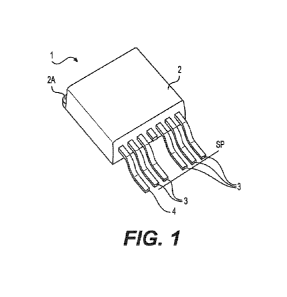
FIG. 1 is a perspective view of a conventional MOSFET having a standard
configuration of the power pins and gate pin. Specifically, the tips of the
power pins and
gate pin are all located is a same plane and along a same axis in the same
plane.
FIG. 2 is a perspective view of a semiconductor device (e.g. MOSFET) according
to the present invention.
FIG. 3 is a side elevational view of the semiconductor device shown in FIG. 2.
FIG. 4 is a side elevational view of the semiconductor device shown in FIGS. 2
and 3 installed onto a printed circuit board of a battery management system
(BMS) for
use in a lithium ion battery.
FIG. 5 is a side elevational view of the semiconductor device shown in FIG. 4
installed onto a printed circuit board of a battery management system (BMS)
for use in a
lithium ion battery showing the connector wire protected.
FIG. 6 is a perspective view of the printed circuit board (PCB) of the battery
management system (BMS) showing multiple semiconductor devices shown in FIGS.
2
and 3 installed onto the printed circuit board (PCB) of a battery management
system
(BMS) for use in a lithium ion battery.
FIG. 7 is a side elevational view of the semiconductor device shown in FIG. 2
installed in an alternative manner onto a printed circuit board of a battery
management
system (BMS) for use in a lithium ion battery.
13
CA 03163239 2022-05-27
WO 2021/108706 PCT/US2020/062417
DETAILED DESCRIPTION
A semiconductor device (e.g. MOSFET 10) according to the present invention is
shown in FIGS. 2 and 3.
The MOSFET 10 comprises a body 12, a metal connector 12A, five (5) power
pins 13, and one (1) gate pin 14. The power pins 13 and gate pin 14 extend
outwardly
from the side of the body 12. The gate pin 14, for example, is a straight gate
pin 14, or a
partially bent gate pin 14 C (FIG. 2), and the power pins 14 are fully bent,
as shown in
FIG. 4).
It is pointed out that the tips of the power pins 13 are located at height H1,
as
shown in FIG. 2. The height of the tip of the partially bent gate pin 14' is
at the height H2
(i.e. half height location), and the height of the tip of the straight gate
pin 14 is at the
height H3 (i.e. full height). Thus, the tip of the partially bent gate pin 14'
and the tip of
the straight gate pin 14 are elevated relative to the tips of the power pins
13 located at
height H1. Thus, after the MOSFET 10 is installed, the tip of the partially
bent gate pin
14' and the tip of the straight gate pin 14 are raised or elevated relative to
the
conductive plate 18 (FIG. 4) to avoid electrically contact therebetween.
As shown in FIGS. 2 and 3, the MOSFET 10 and copper plates 17, 18 are
installed onto the printed circuit board (PCB) 16. Specifically, the copper
plates 17, 18
are spaced apart, and then soldered onto anchors located on the printed
circuit board
(PCB) 16 (e.g. copper plates embedded into the surface or thickness or through
the
printed circuit board (PCB) 16). The MOSFET 10 is then soldered onto the
spaced apart
copper plates 17, 18. Specifically, the metal connector 12A of the MOSFET 10
is
14
CA 03163239 2022-05-27
WO 2021/108706 PCT/US2020/062417
soldered (e.g. via soldered layer 20) onto the copper plate 17, and the tips
of the power
pins 13 of the MOSFET 10 are soldered (e.g. via soldered layer 21) onto the
copper
plate 18. Further, one end of a wire connector 15 is soldered to the gate pin
14, and an
opposite end of the wire connector 15 is soldered (e.g. via soldered layer 19)
onto a
particular trace of the printed circuit board (PCB) 16.
As shown in FIG. 5, a material 22 (e.g. Room Temperature Vulcanizing (RTV)
Silicone) is applied at least between the gate pin 14 and the upper surface of
the printed
circuit board (PCB) 22 to stabilize and support the gate pin 14 and wire
connector 15
against vibration and/or physical shock to prevent breakage of the soldered
connection
between the gate pin 14 and wire connector 15. For example, the material 22 is
applied
by a caulk gun.
Another arrangement for installing one or more MOFETs 112 onto a printed
circuit board (PCB) 116 according to the present invention is shown in FIGS. 6
and 7. A
plurality of MOFETs 112 (e.g. six (6) shown) are installed by soldering onto
the spaced
apart copper plates 118, 117, 118. The tips of the power pins 113 are soldered
onto the
respective copper plates 118. The tips of the gate pins 114 are soldered onto
respective
gate printed circuit boards123 connected to the copper plates 118, 118 (e.g.
by
soldering). Specifically, the gate printed circuit boards 123 are provided
with a plurality
of soldering tabs or soldering areas 124, which are soldered to the respective
tips of the
straight gate pins 114.
The gate printed circuit boards 123 act as insulating spacers located between
the
copper plates 118, 118 and the tips of the gate pins 124. The gate printed
circuit boards
have a conductive trace or a conductive layer that can be connected (e.g.
soldered) to
CA 03163239 2022-05-27
WO 2021/108706 PCT/US2020/062417
other circuits or components of the printed circuit board 116 (e.g. via wire
or conductive
lead(s)).
The gate printed circuit boards 123 occupy the space located between the
copper plates 118 and the tips of the gate pins 114 of the MOSFETs 112, and
insulate
the tips of the gate pins 114 of the MOSFETs 112 from the copper plates 118.
16