Note: Descriptions are shown in the official language in which they were submitted.
WO 2021/146116
PCT/US2021/012759
SILICON-ASSISTED PACKAGING OF HIGH POWER INTEGRATED SOA
ARRAY
CROSS-REFERENCE TO RELATED APPLICATION(S)
[00011 This application claims priority under 35 U.S.C. 119(e)
to U.S. Provisional
Patent Application Serial No. 62/960,688, filed on January 13, 2020, all of
which is
incorporated by reference in its entirely.
TECHNICAL FIELD
[0002] This disclosure relates generally to frequency modulated
continuous wave
(FMCW) light detection and ranging (LiDAR), more particularly, to solid state
FMCW
LiDAR systems
BACKGROUND
[0003] Conventional LiDAR systems use mechanical moving parts
and bulk optical
lens elements (i.e., a refractive lens system) to steer the laser beam. And
for many
applications (e.g., automotive) are too bulky, costly, and unreliable.
SUMMARY
[0004] A photonic integrated circuit (PIC) assembly includes a
semiconductor optical
amplifier (SOA) array and a U-turn chip. The semiconductor optical amplifier
(SOA) array
includes an input SOA and a plurality of SOAs. The input SOA and the plurality
of SOAs are
arranged parallel to one another. The U-turn chip includes an optical splitter
and a waveguide
assembly. The optical splitter is configured to receive amplified input light
propagating in a
first direction from the input SOA, and divide the amplified light into a
plurality of beams.
The waveguide assembly is configured to guide each of the plurality of beams
to a
corresponding SOA of the plurality of SOAs. The waveguide assembly also
adjusts a
direction of propagation of each of the guided beams to be substantially
parallel to a second
direction that is substantially opposite the first direction. Each of the
plurality of SOAs are
configured to amplify their respective beams to generate a plurality of
amplified output
beams. The PIC assembly may be part of, e.g., a frequency modulated continuous
wave
(FMCW) LiDAR system.
1
CA 03163589 2022- 6- 30
WO 2021/146116
PCT/US2021/012759
[0005] In some embodiments, the PIC assembly includes a
semiconductor optical
amplifier (SOA) module. The SOA module includes a SOA array and may also
include a U-
turn chip (in alternate embodiments the U-turn chip may be part of a PIC chip
the SOA
module couples to). The SOA array is on a SOA chip. The SOA array includes an
input SOA
and a plurality of SOAs, and the input SOA and the plurality of SOAs are
arranged parallel to
one another. The U-turn chip is coupled to the SOA chip, and includes an
optical splitter and
a waveguide assembly. The optical splitter is configured to receive amplified
input light
propagating in a first direction from the input SOA, and divide the amplified
light into a
plurality of beams. The waveguide assembly is configured to guide each of the
plurality of
beams to a corresponding SOA of the plurality of SOAs, wherein the waveguide
assembly
adjusts a direction of propagation of each of the guided beams to be
substantially parallel to a
second direction that is substantially opposite the first direction, and
wherein each of the
plurality of SOAs are configured to amplify their respective beams to generate
a plurality of
amplified output beams.
BRIEF DESCRIPTION OF THE DRAWINGS
[0006] Embodiments of the disclosure have other advantages and
features which will be
more readily apparent from the following detailed description and the appended
claims, when
taken in conjunction with the examples in the accompanying drawings, in which:
[0007] Figure 1 shows a top-down view of a photonic integrated
circuit assembly that
includes two SOA array chips and two corresponding U-turn chips that are
coupled to a PIC
chip, according to one or more embodiments.
[0008] Figure 2 depicts the cross section of one embodiment of
an SOA array module,
according to one or more embodiments.
[0009] Figure 3 depicts another embodiment of a cross section of
an SOA array module
coupled to a PIC chip.
[0010] Figures 4A-B describe an example fabrication process,
according to one or more
embodiments.
[0011] Figures 5A-B describes a PIC assembly that includes a
suspended U-turn chip,
according to one or more embodiments.
[0012] Figure 6 describes a PIC assembly that includes a
suspended U-turn chip and a
plurality of comb drives, according to one or more embodiments.
[0013] Figure 7 shows a top-down view of a PIC assembly that
includes an external
cavity laser, according to one or more embodiments.
2
CA 03163589 2022- 6- 30
WO 2021/146116
PCT/US2021/012759
DETAILED DESCRIPTION OF THE PREFERRED EMBODIMENTS
[0014] A SOA module includes a SOA array (on a SOA array chip)
and may include a
U-turn chip (in other embodiments the U-turn chip is part of a PIC circuit to
which the SOA
module couples to), and the SOA module may be coupled to a photonic integrated
circuit
(PIC) chip. The SOA array includes an input SOA and a plurality of SOAs. In
some
embodiments, the input SOA is the same as one or more of the plurality of
SOAs. In
alternate embodiments, the input SOA and the plurality of SOAs may be
different (e.g., have
different levels of amplification). In some embodiments, each of the plurality
of SOAs are
configured to provide a same level of amplification. In other embodiments, at
least one of the
plurality of SOAs provides a different level of amplification than the input
SOA and/or
another SOA of the plurality of SOAs. The input SOA and the plurality of SOAs
may be
arranged parallel to one another. The PIC chip, the U-turn chips, or some
combination thereof
may be made out of silicon, silicon nitride, silicon dioxide, or some
combination thereof,
while the SOA array chip may be made from III-V compound semiconductor
materials
composed of Al, Ga, In, N. P. As and other elements.
[0015] The U-turn chip includes an optical splitter and a
waveguide assembly. The
optical splitter is configured to receive amplified input light propagating in
a first direction
from the input SOA, and divide the amplified light into a plurality of beams.
The waveguide
assembly guides each of the plurality of beams to a corresponding SOA of the
plurality of
SOAs. The waveguide assembly also adjusts a direction of propagation of each
of the guided
beams to be substantially parallel to a second direction that is substantially
opposite the first
direction. In this manner, the light guided by the waveguide assembly performs
a "u-turn"
back toward the SOA array.
[0016] Each of the plurality of SOAs are configured to amplify
their respective beams
to generate a plurality of amplified output beams. As the SOA module may be
part of a
photonic integrated circuit (PIC) assembly, the amplified output beams may be
provided to
the PIC assembly for use in, e.g., a frequency modulated continuous wave
(FMCW) LiDAR
system. A FMCW LiDAR directly measure range and velocity of an object by
directing a
frequency modulated, collimated light beam at the object. The light that is
reflected from the
object is combined with a tapped version of the beam. The frequency of the
resulting beat
tone is proportional to the distance of the object from the LIDAR system once
corrected for
the doppler shift that requires a second measurement. The two measurements,
which may or
may not be performed at the same time, provide both range and velocity
information.
3
CA 03163589 2022- 6- 30
WO 2021/146116
PCT/US2021/012759
[0017] Note that a PIC assembly may include a plurality of SOA
modules, a light
source, and a plurality of waveguides to provide the light from the light
source to the plurality
of SOA modules. The plurality of waveguides may also be arranged to provide a
similar U-
turn functionality. This in combination with the parallel arrangement of the
SOAs and the U-
turn chip facilitate easy integration and packaging of the SOA module with the
PIC chip. In
contrast, typical high-power SOA arrays have optical inputs and outputs on
opposing sides of
the III-V chip. This can make packaging the SOA with other photonics chips
costly and
difficult.
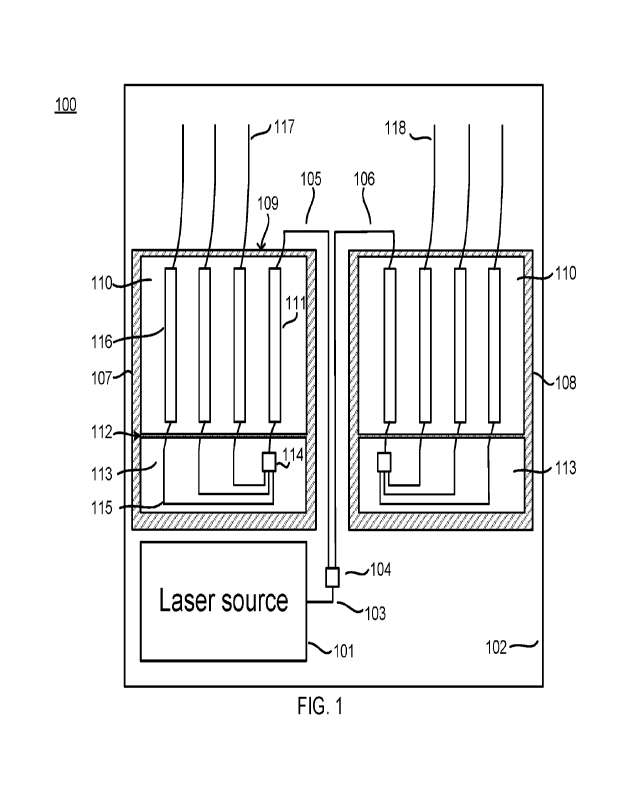
[0018] Figure 1 shows a top-down view of a photonic integrated
circuit (PIC) assembly
100 that includes two SOA array chips 110 (also referred to as an SOA chip)
and two
corresponding U-turn chips 113 coupled to a PIC chip 102, according to one or
more
embodiments. The PIC chip 102, the SOA array chips 110, the U-turn chips 113,
or some
combination thereof may be made out of silicon, silicon nitride, silicon
dioxide, or some
combination thereof
[00191 The output optical power of an integrated laser source
101 sits on top of the PIC
chip 102. The light from this source is coupled into a waveguide 103 which is
patterned on
the PIC chip 102.
[0020] The optical power in the waveguide is split evenly by an
optical divider 104 into
two output waveguides 105 and 106. The optical divider 104 may be, e.g., a
beam splitter.
Although in this example, two SOA modules (i.e., 208 and 208) are
demonstrated, in other
embodiments, a different number of SOA modules may be used. Each of the SOA
modules
107, 108 include a respective SOA array chip 110 (also referred to as a SOA
chip) and the U-
turn chip 113 which are placed in a recessed cavity etched into a top surface
of the PIC 102.
[0021] As shown the output waveguide 105 is configured to
provide the first beam to
the SOA module 107 (and specifically to its corresponding SOA array), and the
output
waveguide 108 is configured to provide the second beam to the SOA module 108
(and
specifically to its corresponding SOA array). Note as shown a direction of
propagation of the
light at entrances of the output waveguide 105 and the output waveguide 106 is
substantially
opposite a direction of propagation at the outputs of the output waveguide 105
and the output
waveguide 106.
[0022] Each SOA array chip includes an SOA array. The SOA array
includes an input
SOA (e.g., input SOA 111) and a plurality of SOAs (e.g., SOA 116). As
illustrated the input
SOAs and the plurality of SOAs are arranged parallel to one another. In other
embodiments,
4
CA 03163589 2022- 6- 30
WO 2021/146116
PCT/US2021/012759
the input SOAs and the plurality of SOAs may have be positioned relative to
one another in a
different manner.
[0023] In the context of the SOA module 107, the output
waveguide 105 is edge-
coupled to the SOA array chip 110 through the front chip facet 109.
[0024] This light passes through the input SOA 111 which acts as
a pre-amplifier to
offset losses associated with chip-to-chip coupling. The light being amplified
is propagating
in a first direction.
[0025] The pre-amplified light is leaving the SOA is edge-
coupled, through the back
facet 112 of the SOA chip 110, to the U-turn chip 113.
[0026] Light in the input waveguide passes through a 1xM
splitter 114 (where M is
equal to one minus the total number of SOAs, including the input SOA, in the
SOA array
110), which equally distributes the pre-amplified optical power between M
waveguides (e.g.,
waveguide 115) of a waveguide assembly. Each waveguide of the waveguide
assembly
incudes a guided beam corresponding to some portion of the pre-amplified
optical power.
[0027] The waveguide assembly adjusts a direction of propagation
of each of the
guided beams to be substantially parallel to a second direction that is
substantially opposite
the first direction. For example, these waveguides are bent around and the
light is coupled
back into the SOA array chip 110 through the back facet 112. Each optical
channel then
passes through a separate SOA 116 on the SOA array chip, amplifying the light
to the desired
output level (i.e., each of the plurality of SOAs are configured to amplify
their respective
beams to generate a plurality of amplified output beams). In some embodiments,
each SOA
116 in an SOA array chip is configured to provide a same level of
amplification. In other
embodiments, at least two of the SOAs 116 have different levels of
amplification. Similarly,
in some embodiments, a plurality of SOA modules on the PIC chip 102 are the
same. And in
other embodiments, at least one SOA module on the PIC chip 102 is different
from another
SOA module on the PIC 102 chip. For example, one SOA module may have a
different
number of SOAs 116 than another SOA module.
[0028] The amplified light is edge-coupled back into the PIC
chip 102 through the front
chip facet 109 and into the waveguide 117. Light from the output waveguide 106
to the SOA
module 108 is amplified in the SOA module 108 in a substantially similar
manner as
described above for the SOA module 107, and is output to waveguide 118.
Waveguides 117
and 118 in the PIC chip 102 carry the light from the packaged SOA arrays to
photonic
circuits contained in the PIC chip 102.
CA 03163589 2022- 6- 30
WO 2021/146116
PCT/US2021/012759
[0029] Figure 2 depicts the cross section of one embodiment of a
SOA array module
200 (also referred to as a SOA module)coupled to a PIC chip 205, according to
one or more
embodiments. A SOA array chip 201 is bonded to a carrier 203 which provides
structural
support and thermal management. Carrier 203 may be made from silicon, other
thermally
conductive ceramics such as AIN or A1203, or some combination thereof The SOA
array
chip 201 may be an embodiment of the SOA array chip 110.
[0030] A U-turn chip 202 is actively coupled to the SOA array
chip 201 with the
assistance of a shim 204 which provides the necessary mechanical offset with
respect to the
carrier 203. Shim 204 may be made from any material although using materials
having
similar coefficient of thermal expansion as that of SOA 201 is advantageous
because
alignment between SOA 201 and U-turn 202 can be better preserved over
temperature
swings. The U-turn chip 202 is an embodiment of the U-turn chip 113. The U-
turn chip 202
is thinned such that the combined module fits in a recess etched into a PIC
chip 205. This
arrangement of bonded SOA array chip 201, carrier 203, shim 204, and U-turn
chip 202 form
the SOA array module 200
[0031] The SOA array module 200 is then placed on the PIC chip
205 which makes use
of the optical power provided by the SOA array chip 201. The PIC chip 205
contains
patterned pedestals 206 which provides mechanical support, precise out-of-
plane alignment,
and a means of fixing the SOA array chip 201 to the PIC chip 205. The SOA
array module is
placed on top of these pedestals 206 and its front facet is brought in close
proximity to a chip
facet 207 and actively aligned to provide efficient optical coupling between
the SOA array
chip 201 and the PIC chip 205. Note that in the illustrated embodiment, the U-
turn chip 202
is on an opposite side of the SOA array chip 201 than the chip facet 207. In
other
embodiments, the location of the chip facet 207 relative to the U-turn chip
202 may vary.
[0032] If needed for additional support, the U-turn chip 202 may
be bonded to the
silicon photonics chip with a low-shrinkage adhesive 208.
[0033] Figure 3 depicts another embodiment of a cross section of
an SOA array module
300 coupled to a PIC chip 304. The SOA array module 300 simplifies the chip
assembling
process, resulting in lower cost for high volume production.
[0034] In this embodiment, the PIC chip 304 and a U-turn chip
302 are fabricated on a
same wafer, so that waveguides 310 in the PIC 304 and waveguides 311 in the U-
turn chip
302 are self-aligned in the vertical direction, i.e., they are at the same
depth below the chip
surface (e.g., are aligned in a same plane). Furthermore, patterned pedestals
(e.g., pedestal
305) in the PIC chip 304 and patterned pedestals (e.g., pedestal 303) in the U-
turn chip 302
6
CA 03163589 2022- 6- 30
WO 2021/146116
PCT/US2021/012759
are formed in such a way that, when the SOA chip 301 is positioned on these
pedestals,
waveguides 309 in the SOA chip 301 align with the waveguides 310 and 311 in
the vertical
direction. Since accurate vertical alignment in the chip assembling process
effects
performance, the mechanical constraints provided by the self-aligned
waveguides 309, 310,
and 311 and the properly formed pedestals significantly improve the yield and
quality of the
final chip assembly, which can lead to higher throughput and lower cost in
manufacturing.
[0035] Figures 4A-B describe an example fabrication process,
according to one or more
embodiments. The process shown in Figures 4A-B may be performed by components
of a
circuit manufacturing system. Other entities may perform some or all of the
steps in Figures
4A-B other embodiments. Embodiments may include different and/or additional
steps, or
perform the steps in different orders.
[0036] As shown in Figure 4A, a PIC 404 and U-turn 402 are
produced on a same
wafer. The wafer may be made out of silicon, silicon nitride, silicon dioxide,
some other
suitable material or some combination thereof Waveguides 410 and 411 are at a
same depth
below the wafer surface. Similarly pedestals 405 and pedestals 403 are formed
such that the
tops of pedestals 405 and the tops of the pedestals 403 are at a same depth
below the wafer
surface. Note that in the illustrated embodiment there are four pedestals 405
and two
pedestals 403. In other embodiments, there may be more or less pedestals 405
and/or more or
less pedestals 403.
[0037] Figure 4B depicts how a SOA module 400 is assembled that
includes a SOA
array chip 401 and a U-turn chip 402. The U-turn chip 402 is cut from the
wafer shown in
Figure 4A, and may be thinned down.
[0038] The SOA array chip 401 is bonded to a carrier 406. The
carrier 406 may be an
embodiment of the carrier 203. Then the U-turn chip 402 is flipped upside
down, aligned, and
bonded to the SOA array chip 401 with the pedestals 403 touching a top surface
of the SOA
array chip 401, thereby providing mechanical constraint in the vertical
direction. Primary
adhesion is supplied by an adhesive (e.g., solder or glue) 408 around the
pedestals 403, while
secondary adhesion may be added using low shrinkage glue 408', along with a
shim 407 if
necessary, between the U-turn chip 402 and the carrier 406 for better
mechanical stability.
Because the height of the pedestals 403 is precisely controlled, this approach
allows for
passive alignment between the SOA array chip 401 and the U-turn chip 402.
[0039] The SOA module 400 is then flipped upside down and bonded
to the PIC chip
404. For example, as shown in Figure 3 the SOA module 400 is then flipped
upside down,
aligned to the waveguide 310 in the PIC 304, and bonded with adhesive 308 in a
recessed
7
CA 03163589 2022- 6- 30
WO 2021/146116
PCT/US2021/012759
cavity that houses the pedestals of the PIC chip 304 (e.g., the pedestal 305)
as mechanical
stop ensuring vertical alignment of the assembly.
[0040] Figures 5A-B describes a PIC assembly 500 that includes a
suspended U-turn
chip 502, according to one or more embodiments. The PIC assembly 500 includes
a PIC chip
505 that is connected to a suspended U-turn chip 502, and a SOA module. The
SOA module
includes a SOA array chip 501 and a carrier 503. Figure 5A is a cross
sectional view of the
PIC assembly 500, and Figure 5B is a top down view of the PIC assembly 500.
The PIC chip
505 and the U-turn chip 502 are fabricated on a same wafer (e.g., similar to
the embodiment
described above with regard to Figures 4A). Instead of cutting it off the
wafer, the U-turn
chip 502 is attached and suspended by flexure 509, when its bottom is hollowed
out with a
cavity or through via 510. The U-turn chip 502 has a little freedom to move in-
plane while
out-of-plane motion is constrained. This ensures vertical direction alignment
between the PIC
505, an SOA array chip 501, and the U-turn chip 502, but allows left/right
movement of the
U-turn chip 502 in order to accommodate variation in the length of the SOA
array chip 501.
During assembly, the pre-assembled SOA 501 on carrier 503 is flipped, aligned,
and bonded
on pedestals (e.g., pedestal 506) of the PIC chip 505. Then the U-turn chip
502 is pushed
toward the SOA array chip 501 and fixed permanently in position with adhesive
508 to form
the PIC assembly 500.
[0041] Figure 6 describes a PIC assembly 600 in which PIC chip
605 includes a
suspended U-turn chip 602 and a plurality of comb drives 611, according to one
or more
embodiments. The comb drives 611 are added to use electro-static force to move
the U-turn
chip 602 in-plane. As illustrated the comb drives 611 are configured control
translation of the
U-turn chip 602 relative to a SOA array chip 601 in two orthogonal directions.
The comb
drives 611 are formed from portions of the U-turn chip 602 and the PIC chip
605, and are
configured to position the U-turn chip 602 relative to the SOA array chip 601.
Once
waveguides in the SOA array chip 601 are aligned with those in the U-turn chip
602, an
adhesive 608 is applied to permanently fix the U-turn chip 602 in position.
While three comb
drives 611 are illustrated, in other embodiments, the PIC chip 605 may include
one or more
comb drives 611.
[0042] Figure 7 shows a top-down view of a PIC assembly 700 that
includes an
external cavity laser, according to one or more embodiments. The PIC assembly
700 includes
one SOA array chip 110 and one gain medium chip 701 packaged to a PIC chip 702
that
includes a resonator 718, with the assistance of the U-turn chip 113. The gain
medium chip
701 and the resonator 718 form the external cavity laser (ECL), which is the
laser source in
8
CA 03163589 2022- 6- 30
WO 2021/146116
PCT/US2021/012759
this embodiment. The resonator 718 and the gain medium chip 701 collectively
select and
amplify a specific band of the emitted light.
[0043] The light from the ECL source is coupled into the SOA
array chip 110 via a
waveguide 705. The SOA array chip 110 operates on the in-coupled light in the
same manner
as described above with regard to Figure 1.
Additional Configuration Information
[0044] The figures and the preceding description relate to
preferred embodiments by
way of illustration only. It should be noted that from the preceding
discussion, alternative
embodiments of the structures and methods disclosed herein will be readily
recognized as
viable alternatives that may be employed without departing from the principles
of what is
claimed.
[0045] Although the detailed description contains many
specifics, these should not be
construed as limiting the scope of the invention but merely as illustrating
different examples.
It should be appreciated that the scope of the disclosure includes other
embodiments not
discussed in detail above. Various other modifications, changes and variations
which will be
apparent to those skilled in the art may be made in the arrangement, operation
and details of
the method and apparatus disclosed herein without departing from the spirit
and scope as
defined in the appended claims. Therefore, the scope of the invention should
be determined
by the appended claims and their legal equivalents.
[0046] Alternate embodiments are implemented in computer
hardware, firmware_
software, and/or combinations thereof Implementations can be implemented in a
computer
program product tangibly embodied in a machine-readable storage device for
execution by a
programmable processor; and method steps can be performed by a programmable
processor
executing a program of instructions to perform functions by operating on input
data and
generating output. Embodiments can be implemented advantageously in one or
more
computer programs that are executable on a programmable system including at
least one
programmable processor coupled to receive data and instructions from, and to
transmit data
and instructions to, a data storage system, at least one input device, and at
least one output
device. Each computer program can be implemented in a high-level procedural or
object-
oriented programming language, or in assembly or machine language if desired;
and in any
case, the language can be a compiled or interpreted language. Suitable
processors include, by
way of example, both general and special purpose microprocessors. Generally, a
processor
will receive instructions and data from a read-only memory and/or a random
access memory.
9
CA 03163589 2022- 6- 30
WO 2021/146116
PCT/US2021/012759
Generally, a computer will include one or more mass storage devices for
storing data files;
such devices include magnetic disks, such as internal hard disks and removable
disks;
magneto-optical disks; and optical disks. Storage devices suitable for
tangibly embodying
computer program instructions and data include all forms of non-volatile
memory, including
by way of example semiconductor memory devices, such as EPROM, EEPROM, and
flash
memory devices; magnetic disks such as internal hard disks and removable
disks; magneto-
optical disks; and CD-ROM disks. Any of the foregoing can be supplemented by,
or
incorporated in, ASICs (application-specific integrated circuits) and other
forms of hardware.
CA 03163589 2022- 6- 30