Note: Descriptions are shown in the official language in which they were submitted.
CA 03163679 2022-06-01
WO 2021/133541
PCT/US2020/063578
TRANSFERABLE LIGHT-TRANSMISSIVE ELECTRODE FILMS FOR
ELECTRO-OPTIC DEVICES
RELATED APPLICATIONS
[Para 1] This application claims priority to U.S. Provisional Patent
Application No.
62/952,600 filed on December 23, 2019, which is incorporated by reference in
its
entirety, along with all other patents and patent applications disclosed
herein.
BACKGROUND OF INVENTION
[Para 2] This invention relates to electro-optic devices and to materials for
use therein.
More specifically, this invention relates to an electro-optic device having
improved
electro-optic performance. The electro-optic device comprises a conductive
film
comprising a first adhesive layer and a first electrode layer, wherein the
first electrode
layer comprises a conductive material selected from the group consisting of
conductive
particles, a metallic material and a conductive polymer. The invention also
relates to a
method of manufacturing of an electro-optic device. The present invention is
especial I y,
though not exclusively, intended for use in displays containing encapsulated
electrophoretic media.
[Para 3] The term "electro-optic", as applied to a material, a display, or a
device, is
used herein in its conventional meaning in the imaging art to refer to a
material having
first and second display states differing in at least one optical property,
the material
being changed from its first to its second display state by application of an
electric field
to the material. Although the optical property is typically color perceptible
to the human
eye, it may be another optical property, such as optical transmission,
reflectance,
luminescence or, in the case of displays intended for machine reading, pseudo-
color in
the sense of a change in reflectance of electromagnetic wavelengths outside
the visible
range.
[Para 4] The term "gray state" is used herein in its conventional meaning in
the
imaging art to refer to a state intermediate two extreme optical states of a
pixel, and
does not necessarily imply a black-white transition between these two extreme
states.
For example, several of the E Ink patents and published applications referred
to below
describe electrophoretic displays in which the extreme states are white and
deep blue,
so that an intermediate "gray state" would actually be pale blue. Indeed, as
already
1
CA 03163679 2022-06-01
WO 2021/133541
PCT/US2020/063578
mentioned, the change in optical state may not be a color change at all. The
terms
"black" and "white" may be used hereinafter to refer to the two extreme
optical states
of a display, and should be understood as normally including extreme optical
states
which are not strictly black and white, for example the aforementioned white
and dark
blue states. The term "monochrome" may be used hereinafter to denote a drive
scheme,
which only drives pixels to their two extreme optical states with no
intervening gray
states.
[Para 5] Some electro-optic materials are solid in the sense that the
materials have
solid external surfaces, although the materials may, and often do, have
internal liquid-
or gas-filled spaces. Such displays using solid electro-optic materials may
hereinafter
for convenience be referred to as "solid electro-optic displays". Thus, the
term "solid
electro-optic displays" includes rotating bichromal member displays,
encapsulated
electrophoretic displays, microcell electrophoretic displays and encapsulated
liquid
crystal displays.
[Para 6] The terms "bistable" and "bistability" are used herein in their
conventional
meaning in the art to refer to displays comprising display elements having
first and
second display states differing in at least one optical property, and such
that after any
given element has been driven, by means of an addressing pulse of finite
duration, to
assume either its first or second display state, after the addressing pulse
has terminated,
that state will persist for at least several times, for example at least four
times, the
minimum duration of the addressing pulse required to change the state of the
display
element. It is shown in U.S. Patent No. 7,170,670 that some particle-based
electrophoretic displays capable of gray scale are stable not only in their
extreme black
and white states but also in their intermediate gray states, and the same is
true of some
other types of electro-optic displays. This type of display is properly called
"multi-
stable" rather than bistable, although for convenience the term "bistable" may
be used
herein to cover both bistable and multi-stable displays.
[Para 7] Several types of electro-optic displays are known. One type of
electro-optic
display is a rotating bichromal member type as described, for example, in U.S.
Patents
Nos. 5,808,783; 5,777,782; 5,760,761; 6,054,071 6,055,091; 6,097,531;
6,128,124;
6,137,467; and 6,147,791 (although this type of display is often referred to
as a "rotating
bichromal ball" display, the term "rotating bichromal member" is preferred as
more
accurate since in some of the patents mentioned above the rotating members are
not
2
CA 03163679 2022-06-01
WO 2021/133541
PCT/US2020/063578
spherical). Such a display uses a large number of small bodies (typically
spherical or
cylindrical) which have two or more sections with differing optical
characteristics, and
an internal dipole. These bodies are suspended within liquid-filled vacuoles
within a
matrix, the vacuoles being filled with liquid so that the bodies are free to
rotate. The
appearance of the display is changed by applying an electric field thereto,
thus rotating
the bodies to various positions and varying which of the sections of the
bodies is seen
through a viewing surface. This type of electro-optic medium is typically
bistable.
[Para 8] Another type of electro-optic display uses an electrochromic medium,
for
example an electrochromic medium in the form of a nanochromic film comprising
an
electrode formed at least in part from a semi-conducting metal oxide and a
plurality of
dye molecules capable of reversible color change attached to the electrode;
see, for
example O'Regan, B., et al., Nature 1991, 353, 737; and Wood, D., Information
Display, 18(3), 24 (March 2002). See also Bach, U., et al., Adv. Mater., 2002,
14(11),
845. Nanochromic films of this type are also described, for example, in U.S.
Patents
Nos. 6,301,038; 6,870,657; and 6,950,220. This type of medium is also
typically
bistable.
[Para 9] Another type of electro-optic display is an electro-wetting display
developed by Philips and described in Hayes, R.A., et al., "Video-Speed
Electronic
Paper Based on Electrowetting", Nature, 425, 383-385 (2003). It is shown in
U.S.
Patent No. 7,420,549 that such electro-wetting displays can be made bistable.
[Para 1 0] One type of electro-optic display, which has been the subject of
intense
research and development for a number of years, is the particle-based
electrophoretic
display, in which a plurality of charged particles move through a fluid under
the
influence of an electric field. Electrophoretic displays can have attributes
of good
brightness and contrast, wide viewing angles, state bistability, and low power
consumption when compared with liquid crystal displays. Nevertheless, problems
with
the long-term image quality of these displays have prevented their widespread
usage.
For example, particles that make up electrophoretic displays tend to settle,
resulting in
inadequate service-life for these displays.
[Para 1 1 ] As noted above, electrophoretic media require the presence of a
fluid. In
most prior art electrophoretic media, this fluid is a liquid, but
electrophoretic media can
be produced using gaseous fluids; see, for example, Kitamura, T., et al.,
"Electrical
toner movement for electronic paper-like display", IDW Japan, 2001, Paper HCS1-
1,
3
CA 03163679 2022-06-01
WO 2021/133541
PCT/US2020/063578
and Yamaguchi, Y., et al., "Toner display using insulative particles charged
triboelectrically", IDW Japan, 2001, Paper AMD4-4). See also U.S. Patents Nos.
7,321,459 and 7,236,291. Such gas-based electrophoretic media appear to be
susceptible to the same types of problems due to particle settling as liquid-
based
electrophoretic media, when the media are used in an orientation which permits
such
settling, for example in a sign where the medium is disposed in a vertical
plane. Indeed,
particle settling appears to be a more serious problem in gas-based
electrophoretic
media than in liquid-based ones, since the lower viscosity of gaseous
suspending fluids
as compared with liquid ones allows more rapid settling of the electrophoretic
particles.
[Para 1 2] Numerous patents and applications assigned to or in the names of
the
Massachusetts Institute of Technology (MIT), E Ink Corporation, E Ink
California,
LLC and related companies describe various technologies used in encapsulated
and
microcell electrophoretic and other electro-optic media. Encapsulated
electrophoretic
media comprise numerous small capsules, each of which itself comprises an
internal
phase containing electrophoretically mobile particles in a fluid medium, and a
capsule
wall surrounding the internal phase. Typically, the capsules are themselves
held within
a polymeric binder to form a coherent layer positioned between two electrodes.
In a
microcell electrophoretic display, the charged particles and the fluid are not
encapsulated within microcapsules but instead are retained within a plurality
of cavities
formed within a carrier medium, typically a polymeric film. The technologies
described
in these patents and applications include:
(a) Electrophoretic particles, fluids and fluid additives; see for example
U.S.
Patents Nos. 7,002,728; 7,679,814;
(b) Capsules, binders and encapsulation processes; see for example U.S.
Patents Nos. 6,922,276; 7,411,719; and U.S. Patent Applications Publication
Nos.
US2017/0251155;
(c) Microcell structures, wall materials, and methods of forming
microcells;
see for example United States Patents Nos. 7,072,095; 9,279,906;
(d) Methods for filling and sealing microcells; see for example United
States Patents Nos. 7,144,942; 7,715,088;
(e) Films and sub-assemblies containing electro-optic materials; see for
example U.S. Patents Nos. 6,982,178; 7,839,564; and 9,835,925;
4
CA 03163679 2022-06-01
WO 2021/133541
PCT/US2020/063578
(f) Backplanes, adhesive layers and other auxiliary layers and methods used
in displays; see for example U.S. Patents Nos 7,116,318; 7,535,624; 7,672,040;
7,173,752; 7,342,068; and International Application Publication No. WO
2007/121104;
(g) Color formation and color adjustment; see for example U.S. Patents
Nos. 7,075,502; 7,839,564;
(h) Methods for driving displays; see for example U.S. Patents Nos.
7,012,600; 7,453,445;
(i) Applications of displays; see for example U.S. Patents Nos. 7,312,784;
8,009,348; and
Non-electrophoretic displays, as described in U.S. Patents Nos.
6,241,921; and U.S. Patent Application Publication No. 2015/0277160; and
applications of encapsulation and microcell technology other than displays;
see for
example United States Patent Application Publications Nos. 2015/0005720 and
2016/0012710.
[Para 1 3] Many of the aforementioned patents and applications recognize that
the
walls surrounding the discrete microcapsules in an encapsulated
electrophoretic
medium could be replaced by a continuous phase, thus producing a so-called
polymer-
dispersed electrophoretic display, in which the electrophoretic medium
comprises a
plurality of discrete droplets of an electrophoretic fluid and a continuous
phase of a
polymeric material, and that the discrete droplets of electrophoretic fluid
within such a
polymer-dispersed electrophoretic display may be regarded as capsules or
microcapsules, even though no discrete capsule membrane is associated with
each
individual droplet; see for example, the aforementioned U.S. Patent No.
6,866,760.
Accordingly, for purposes of the present application, such polymer-dispersed
electrophoretic media are regarded as sub-species of encapsulated
electrophoretic
media.
[Para 1 4] Although electrophoretic media are often opaque (since, for
example, in
many electrophoretic media, the particles substantially block transmission of
visible
light through the display) and operate in a reflective mode, many
electrophoretic
displays can be made to operate in a so-called "shutter mode" in which one
display state
is substantially opaque and one is light-transmissive. See, for example, U.S.
Patents
Nos. 5,872,552; 6,130,774; 6,144,361; 6,172,798; 6,271,823; 6,225,971; and
6,184,856. Dielectrophoretic displays, which are similar to electrophoretic
displays but
CA 03163679 2022-06-01
WO 2021/133541
PCT/US2020/063578
rely upon variations in electric field strength, can operate in a similar
mode; see U.S.
Patent No. 4,418,346. Other types of electro-optic displays may also be
capable of
operating in shutter mode. Electro-optic media operating in shutter mode may
be useful
in multi-layer structures for full color displays; in such structures, at
least one layer
adjacent the viewing surface of the display operates in shutter mode to expose
or
conceal a second layer more distant from the viewing surface.
[Para 1 5] An encapsulated electrophoretic display typically does not suffer
from the
clustering and settling failure mode of traditional electrophoretic devices
and provides
further advantages, such as the ability to print or coat the display on a wide
variety of
flexible and rigid substrates. Use of the word "printing" is intended to
include all forms
of printing and coating, including, but without limitation: pre-metered
coatings such as
patch die coating, slot or extrusion coating, slide or cascade coating,
curtain coating;
roll coating such as knife over roll coating, forward and reverse roll
coating; gravure
coating; dip coating; spray coating; meniscus coating; spin coating; brush
coating; air
knife coating; silk screen printing processes; electrostatic printing
processes; thermal
printing processes; ink jet printing processes; electrophoretic deposition
(See U.S.
Patent No. 7,339,715); and other similar techniques. Thus, the resulting
display can be
flexible. Further, because the display medium can be printed (using a variety
of
methods), the display itself can be made inexpensively.
[Para 1 6] Other types of electro-optic materials may also be used in the
present
invention. Of particular interest, bistable ferroelectric liquid crystal
displays (FLC's)
are known in the art.
[Para 1 7] An electro-optic device may typically comprise a plurality of
functional
layers, including, but not limited to, a front electrode, an electro-optic
material layer,
and a back electrode. For example, in some ei ectrophoreti c dispiays, the
etectro-optie
material laver may include a plurality of capsules that are distributed in a
binder. In
most such devices, both the layers are electrode layers, and one or both of
the electrode
layers are patterned to define the pixels of the display. For example, one
electrode layer
may be patterned into elongate row electrodes and the other into elongate
column
electrodes running at right angles to the row electrodes, the pixels being
defined by the
intersections of the row and column electrodes. Alternatively, and more
commonly, one
electrode layer has the form of a single continuous electrode and the other
electrode
layer is patterned into a matrix of pixel electrodes, each of which defines
one pixel of
6
CA 03163679 2022-06-01
WO 2021/133541
PCT/US2020/063578
the display. In another type of electrophoretic display, which is intended for
use with a
stylus, print head or similar movable electrode separate from the display,
only one of
the layers adjacent the electrophoretic layer comprises an electrode, the
layer on the
opposed side of the electrophoretic layer typically being a protective layer
intended to
prevent the movable electrode damaging the electrophoretic layer.
[Para 1 8] The manufacture of a three-layer electrophoretic display normally
involves
at least one lamination operation. For example, in several of the
aforementioned MIT
and E Ink patents and applications, there is described a process for
manufacturing an
encapsulated electrophoretic display in which an encapsulated electrophoretic
medium
comprising capsules in a binder is coated on to a flexible substrate
comprising indium-
tin-oxide (ITO) or a similar conductive coating (which acts as one electrode
of the final
display) on a plastic film, the capsules/binder coating being dried to form a
coherent
layer of the electrophoretic medium firmly adhered to the substrate.
Separately, a
backplane, containing an array of pixel electrodes and an appropriate
arrangement of
conductors to connect the pixel electrodes to drive circuitry, is prepared. To
form the
final display, the substrate having the capsule/binder layer thereon is
laminated to the
backplane using a lamination adhesive. A very similar process can be used to
prepare
an electrophoretic display usable with a stylus or similar movable electrode
by
replacing the backplane with a simple protective layer, such as a plastic
film, over
which the stylus or other movable electrode can slide. In one preferred form
of such a
process, the backplane is itself flexible and is prepared by printing the
pixel electrodes
and conductors on a plastic film or other flexible substrate. The obvious
lamination
technique for mass production of displays by this process is roll lamination
using a
lamination adhesive.
[Para 1 9] The aforementioned U.S. Patent No. 6,982,178 describes a method of
assembling a solid electro-optic display (including an encapsulated
electrophoretic
display) which is well adapted for mass production. Essentially, this patent
describes a
so-called "front plane laminate" ("FPL") which comprises, in order, a light-
transmissive
electrically conductive layer; a layer of a solid electro-optic medium in
electrical
contact with the electrically conductive layer; an adhesive layer; and a
release sheet.
Typically, the light-transmissive electrically conductive layer will be
carried on a light-
transmissive substrate, which is preferably flexible, in the sense that the
substrate can
be manually wrapped around a drum (say) 10 inches (254 mm) in diameter without
7
CA 03163679 2022-06-01
WO 2021/133541
PCT/US2020/063578
permanent deformation. The term "light-transmissive" is used in this patent
and herein
to mean that the layer thus designated transmits sufficient light to enable an
observer,
looking through that layer, to observe the change in display states of the
electro-optic
medium, which will normally be viewed through the electrically-conductive
layer and
adjacent substrate (if present); in cases where the electro-optic medium
displays a
change in reflectivity at non-visible wavelengths, the term "light-
transmissive" should
of course be interpreted to refer to transmission of the relevant non-visible
wavelengths.
The substrate will typically be a polymeric film, and will normally have a
thickness in
the range of about 1 to about 25 mil (25 to 634 m), preferably about 2 to
about 10 mil
(51 to 254 m). The electrically-conductive layer is conveniently a thin metal
or metal
oxide layer of, for example, aluminum or ITO, or may be a conductive polymer.
Poly(ethylene terephthalate) (PET) films coated with aluminum or ITO are
available
commercially, for example as "aluminized Mylar" ("Mylar" is a Registered Trade
Mark) from E.I. du Pont de Nemours & Company, Wilmington DE, and such
commercial materials may be used with good results in the front plane
laminate.
[Para 20] Assembly of an electro-optic display using such a front plane
laminate may
be effected by removing the release sheet from the front plane laminate and
contacting
the adhesive layer with the backplane under conditions effective to cause the
adhesive
layer to adhere to the backplane, thereby securing the adhesive layer, layer
of electro-
optic medium and electrically-conductive layer to the backplane. This process
is well
adapted to mass production since the front plane laminate may be mass-
produced,
typically using roll-to-roll coating techniques, and then cut into pieces of
any size
needed for use with specific backplanes.
[Para 21] U.S. Patent No. 7,561,324 describes a so-called "double release
sheet"
which is essentially a simplified version of the front plane laminate of the
aforementioned U.S. Patent No. 6,982,178. One form of the double release sheet
comprises a layer of a solid electro-optic medium sandwiched between two
adhesive
layers, one or both of the adhesive layers being covered by a release sheet.
Another
form of the double release sheet comprises a layer of a solid electro-optic
medium
sandwiched between two release sheets. Both forms of the double release film
are
intended for use in a process generally similar to the process for assembling
an electro-
optic display from a front plane laminate already described, but involving two
separate
laminations; typically, in a first lamination the double release sheet is
laminated to a
8
CA 03163679 2022-06-01
WO 2021/133541
PCT/US2020/063578
front electrode to form a front sub-assembly, and then in a second lamination
the front
sub-assembly is laminated to a backplane to form the final display, although
the order
of these two laminations could be reversed if desired.
[Para 22] U. S. Patent No. 7,839,564 describes a so-called "inverted front
plane
laminate", which is a variant of the front plane laminate described in the
aforementioned
U.S. Patent No. 6,982,178. This inverted front plane laminate comprises, in
order, at
least one of a light-transmissive protective layer and a light-transmissive
electrically-
conductive layer; an adhesive layer; a layer of a solid electro-optic medium;
and a
release sheet. This inverted front plane laminate is used to form an electro-
optic display
having a layer of lamination adhesive between the electro-optic layer and the
front
electrode or front substrate; a second, typically thin layer of adhesive may
or may not
be present between the electro-optic layer and a backplane. Such electro-optic
displays
can combine good resolution with good low temperature performance.
[Para 23] The aforementioned 2007/0109219 also describes various methods
designed for high volume manufacture of electro-optic displays using inverted
front
plane laminates; preferred forms of these methods are "multi-up" methods
designed to
allow lamination of components for a plurality of electro-optic displays at
one time.
[Para 24] In the processes described above, the lamination of the substrate
carrying
the electro-optic layer to the backplane may advantageously be carried out by
vacuum
lamination. Vacuum lamination is effective in expelling air from between the
two
materials being laminated, thus avoiding unwanted air bubbles in the final
display; such
air bubbles may introduce undesirable artifacts in the images produced on the
display.
[Para 25] The front electrode of a typical electro-optic devices comprises a
continuous film of Indium Tin Oxide (ITO), which is in electrical contact with
the
electro-optic material layer. In many cases, an adhesive layer is interposed
between the
front and back electrode within the electro-optic device. The interposition of
the
adhesive layer improves the mechanical stability of the device, but it may
also (a)
increase the cost of manufacturing, (b) increase the required voltage and
energy
consumption to drive the device, (c) decrease the operational temperature
range, and
(d) decrease the switching speed. Thus, there is a need for the development of
electro-
optic devices with improved performance. The invention of the present patent
application avoids the above-mentioned drawbacks by eliminating the need for
an
adhesive layer between the front electrode and back electrode of the electro-
optic
9
CA 03163679 2022-06-01
WO 2021/133541
PCT/US2020/063578
device. The invention also enables the construction of flexible electro-optic
devices
having a thin, flexible and light-transmissive front electrode. In addition,
the invention
enables the preservation of good electro-optic performance of an electro-optic
device
even in the case of coating defects or voids in the electro-optic material
layer.
SUMMARY
[Para 26] Accordingly, in one aspect, this invention provides an electro-optic
device
comprising a first substrate layer, a conductive film comprising a first
adhesive layer
and a first electrode layer, an electro-optic material layer, and a second
electrode layer.
The first electrode layer comprises a conductive material and has a first
surface and
second surface. The electro-optic material layer has a first surface and a
second surface.
The first surface of the first electrode layer is in contact with the first
adhesive layer.
The second surface of the first electrode layer is in contact with the first
surface of the
electro-optic material layer. The conductive film may be light-transmissive.
The
conductive film may be flexible. The conductive film does not conform to the
surface
roughness of the first surface of the electro-optic material layer. The first
adhesive layer
of the conductive film may have a storage modulus G' of at least 104 Pa
measured at
frequency of 10-3 Hz and temperature of 70 C. The first substrate layer, the
conductive
film, the electro-optic material layer, and the second electrode layer of the
electro-optic
device may be arranged in this order. The first substrate layer may be a first
release
film. The electro-optic device may also comprise a second substrate layer,
wherein the
second electrode layer is interposed between the electro-optic material layer
and the
second substrate layer. The second substrate layer may be a second release
sheet, which
is attached to the second electrode via a second adhesive layer. The second
electrode
layer may comprise one electrode or a plurality of electrodes. The plurality
of electrodes
is also called pixel electrodes. The electro-optic device may be flexible.
[Para 27] The first electrode layer of the electro-optic device may comprise a
metallic
material, a conductive polymer, conductive particles, or combinations thereof
The
conductive particles may be conductive carbon black, single walled carbon
nanotubes,
multiple walled carbon nanotubes, graphene, conductive metal oxide particles
or
combinations thereof The metallic material may comprise metal particles, metal
nanoparticles, metal wires, metal nanowires, metal fibers, metal nanofibers,
metal
flakes, metal disks or combinations thereof.
CA 03163679 2022-06-01
WO 2021/133541
PCT/US2020/063578
[Para 28] The electro-optic material layer of the electro-optic device may
comprise
an encapsulated electrophoretic medium including an internal phase, comprising
a
nonpolar liquid and a plurality of dispersed charged pigment particles, and a
polymeric
binder. The electrophoretic medium may be encapsulated in a plurality of
capsules
having an average capsule diameter of from about 30 i_tm to about 120 1_1111.
[Para 29] In another aspect, the invention provides a method of manufacturing
of an
electro-optic device comprising the steps of (1) preparing a conductive sheet
comprising a first electrode layer by (a) coating a conductive dispersion
comprising a
conductive material onto a first release sheet, and (b) drying the conductive
dispersion
to produce a first electrode layer on the first release sheet; (2) preparing a
substrate
sheet by (a) coating a first adhesive composition onto a first substrate layer
and (b)
drying or curing the first adhesive composition to form a first adhesive
layer; (3)
preparing a conductive web by transferring the conductive sheet onto the
substrate
sheet, wherein the first electrode layer of the conductive sheet is in contact
with the first
adhesive layer of the substrate sheet, and wherein the first adhesive layer
and the first
electrode layer make up a conductive film; (4) preparing an electro-optic
module
precursor by coating an electro-optic medium onto a second electrode layer to
form an
electro-optic material layer on the second electrode layer; (5) contacting the
first
electrode layer of the conductive web with the electro-optic material layer of
the
electro-optic module precursor, wherein the conductive film of the electro-
optic device
does not conform to the surface roughness of the electro-optic material layer.
The
conductive sheet may be light-transmissive. The % total light transmittance of
the
conductive sheet may be higher than 60%, or higher than 70%, or higher than
80%, or
higher than 90%, or higher than 95%. The conductive sheet may be flexible. The
first
adhesive layer of the conductive film may have a storage modulus G' of at
least 104 Pa
measured at frequency of 10-3 Hz and temperature of 70 C.
[Para 30] In another aspect, the invention provides a method of manufacturing
of an
electro-optic device comprising the steps of (1) preparing a substrate sheet
by (a)
coating a first adhesive composition on a first substrate layer and (b) drying
or curing
the first adhesive composition to form a first adhesive layer on the first
substrate layer;
(2) preparing a conductive tape by (a) coating a conductive dispersion
comprising a
conductive material onto the first adhesive layer, and (b) drying the
conductive
dispersion to form a first electrode layer, wherein the first electrode layer
and the first
11
CA 03163679 2022-06-01
WO 2021/133541
PCT/US2020/063578
adhesive layer make up an adhesive film; (3) preparing an electro-optic module
precursor by coating an electro-optic medium onto a second electrode layer to
form an
electro-optic material layer on the second electrode layer; (4) contacting the
first
electrode layer of the conductive tape with the electro-optic material layer
of the
electro-optic module precursor, wherein the conductive film does not conform
to the
surface roughness of the electro-optic material layer. The conductive tape is
light-
transmissive. The conductive film may be flexible. The % total light
transmittance of
the conductive tape may be higher than 60%, or higher than 70%, or higher than
80%,
or higher than 90%, or higher than 95%. The first adhesive layer of the
conductive film
may have a storage modulus G' of at least 104Pa measured at frequency of 10-3
Hz and
temperature of 70 C.
BRIEF DESCRIPTION OF THE DRAWINGS
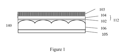
[Para 31] Figure 1 illustrates an embodiment of an electro-optic device
comprising a
first substrate layer, a conductive film comprising first adhesive layer and a
first
electrode layer, an electro-optic material layer, and a second electrode
layer.
[Para 32] Figure 2 is a microphotograph of an embodiment of an electro-optic
device
constructed using the methods of the invention.
[Para 33] Figures 3A and 3B provide an illustration of an example of a process
of
manufacturing of the inventive electro-optic device using a transfer step of
the
conductive film onto the electro-optical material layer.
[Para 34] Figures 4 provides an illustration of an example of a process of
manufacturing of the inventive electro-optic device using a coating step of
the
conductive film on the electro-optical material layer.
DETAILED DESCRIPTION
[Para 35] As used herein, the term "conductive" is synonymous to "electrically-
conductive" and not necessarily to other types of conductivity, such as
thermally
conductive or magnetically conductive, etc., unless otherwise stated.
[Para 36] As used herein, the term "in contact" with respect to two layer
means that
a location of a surface of one of the layers is within a distance of 10 nm of
a location of
the surface of the other layer. The two layers "in contact" may also have a
volume
wherein a material that forms one layer penetrate into the other layer.
12
CA 03163679 2022-06-01
WO 2021/133541
PCT/US2020/063578
[Para 37] As used herein, the term "substantially planar" with respect to a
layer
surface means that all points of the surface fall within the same plane or
within a
distance of less than 10 p.m from a plane.
[Para 38] As used herein, the term "does not conform to the surface roughness"
with
respect to a layer A not conforming to the surface of a layer B means that,
under the
conditions of the manufacturing, storage, and operation of the electro-optic
device,
layer A will only conform to occupy less than 30% of the volume of the
roughness of
the surface of layer B for roughness gaps that have depth of more than 10 m.
Depth is
the dimension from the surface of the layer vertically from the surface.
[Para 39] The term "flexible" is used herein consistently with its normal
meaning in
the display art to refer to a device which is capable of being bent repeatedly
without
macroscopic damage to the display.
[Para 40] The % total light transmittance of a film or a layer or a sheet is
the ratio of
total energy of transmitted light from the film or layer to the energy of the
incident light
x 100. The % total light transmittance is measured with standard method ISO
13468
using D65 illuminant using a spectrophotometer.
[Para 41] As used herein, "molecular weight" refers to weight average
molecular
weight, unless otherwise stated. Molecular weight is measured using industry
standard
size exclusion column chromatography.
[Para 42] The storage modulus values of adhesive layers provided herein are
measured via the Storage Modulus Measurement Method described in the Examples
section.
[Para 43] In one aspect, the present invention provides an electro-optic
device that
comprises a first substrate layer, a conductive film comprising a first
adhesive layer and
a first electrode layer, an electro-optic material layer, and a second
electrode layer.
[Para 44] The first electrode layer comprises a conductive material and has a
first
surface and a second surface. The electro-optic material layer has a first
surface and a
second surface. The electro-optic material layer may comprise a plurality of
microcapsules or a plurality of microcells. The first surface of the first
electrode layer
is in contact with the first adhesive layer; the second surface of the first
electrode layer
is in contact with the electro-optic material layer. The second surface of the
electro-
optic material layer is in contact with a second electrode layer. The electro-
optic device
may also comprise a second substrate layer, wherein the second electrode layer
is
13
CA 03163679 2022-06-01
WO 2021/133541
PCT/US2020/063578
interposed between the electro-optic material layer and the second substrate.
The first
adhesive layer of the conductive film may have a storage modulus G' of at
least 104 Pa
measured at frequency of 10-3 Hz and temperature of 70 C, more preferably
3x10⁴ Pa,
even more preferably 5x10⁴ Pa. This contributes to the fact that the
conductive film
does not conform to the surface roughness of the first surface of the electro-
optic
material layer. As a result, a good electro-optic performance of the electro-
optic device
is preserved even in cases of defects or voids (pinholes) at certain locations
of the
electro-optic material layer. If the conductive film were conforming to the
gaps of the
first surface of the electro-optic material layer, the first electrode layer
could be in
electrical connection with the second electrode layer. In this case, there
would be a short
in the circuit at the location of the gap, leading to a non-optimal electro-
optic
performance.
[Para 45] The first substrate layer may be a first release sheet. The second
substrate
may also be a second release sheet, which may be attached to the second
electrode via
a second adhesive layer. This may be particularly helpful because the release
sheet may
be removed and the device may be attached to any of a variety of substrates or
components.
[Para 46] In one embodiment, the electro-optic device comprises layers that
are
vertically stacked upon each other and the layers have planar surfaces.
Examples of
such devices are two-dimensional devices, such as e readers, computer screens,
mobile
phone screens, etc. In this embodiment, the conductive film is substantially
planar and
it does not conform to the non-planar defects of the electro-optic material
layer.
[Para 47] Another aspect of the present invention involves methods of
manufacturing
of an electro-optic device. In one embodiment, the method of manufacturing
comprises
a transfer step which of a first electrode layer onto a first adhesive layer.
The first
electrode layer and the first adhesive layer make up a conductive film. The
produced
structure, which also comprises a first release sheet, is contacted, after the
removal of
the first release sheet, with an electro-optic module precursor comprising an
electro-
optic material layer and a second electrode layer. This method involves a
lamination
process.
[Para 48] In another embodiment, the method of manufacturing comprises a step
of
coating of a first electrode layer onto a first adhesive layer. The produced
conductive
film is contacted with an electro-optic module precursor comprising an electro-
optic
14
CA 03163679 2022-06-01
WO 2021/133541
PCT/US2020/063578
material layer and a second electrode layer to complete the manufacturing of
the
electro-optic device. This method involves multiple coating steps.
[Para 49] The conductive film may be light-transmissive. The % total light
transmittance of the conductive film may be higher than 60%, or higher than
70%, or
higher than 80%, or higher than 90%, or higher than 95%. The conductive film
may
also be flexible.
[Para 50] An example of an embodiment of the inventive electro-optic device is
provided in Figure 1. The electro-optic device 140 of Figure 1 comprises a
first
substrate layer 103, a conductive film 112 comprising a first adhesive layer
104 and a
first electrode layer 102. The first electrode layer 102 is in contact with an
electro-optic
material layer 106, which is in contact with the second electrode layer 105.
[Para 51] A microphotograph of a vertical cross-section of an electro-optic
device of
the present invention is provided in Figure 2. The electro-optic device 140
comprises a
first substrate layer 103, a conductive film 112, an electro-optic material
layer 106, and
a second electrode layer 105. The darker colored areas of the electro-optic
material
layer 216 (circled) correspond to gaps that are located close to its first
surface. The
electro-optic device was sliced using a razor and a microphotograph of the
vertical cross
section was acquired. The microphotograph shows that the second surface of the
conductive film 112 does not conform to the first surface roughness of the
electro-optic
material layer.
[Para 52] An example of a method of manufacturing of an inventive electro-
optic
device 140 is illustrated in Figures 3A and 3B. More specifically, the method
comprises
a step of a preparation of a conductive sheet 110 by coating a conductive
dispersion
onto a first release sheet 101. The conductive dispersion comprises a
conductive
material and a carrier. After drying of the conductive dispersion, a first
electrode layer
102 is formed on the first release sheet 101, completing the preparation of
the
conductive sheet 110. The method also comprises a step of a preparation of a
substrate
sheet 113 by coating a first adhesive composition on a first substrate layer
103. Drying
or curing of the first adhesive composition completes the preparation of the
substrate
sheet 113, comprising a first adhesive layer 104. Connection of the conductive
sheet
110 with the substrate sheet 113 forms a conductive web 120. This is achieved
by
contacting the first electrode layer 102 of the conductive sheet 110 with the
first
adhesive layer 104 of the substrate sheet. Thus, the conductive web 120
comprises in
CA 03163679 2022-06-01
WO 2021/133541
PCT/US2020/063578
order a first substrate layer 103, a first adhesive layer 104, a first
electrode layer 102,
and a first release sheet 101. The first adhesive layer and the first
electrode layer make
up a conductive film 112. The method of manufacturing also comprises a step of
a
preparation of an electro-optic module precursor 130. This is achieved by
coating an
electro-optic medium onto a second electrode 105. The electro-optic device 140
is
finally formed by removing the first release sheet 101 from the conductive web
120 and
by contacting the exposed surface of the first electrode layer 102 of the
conductive web
120 with the electro-optic material layer 106 of the electro-optic module
precursor 130.
The conductive film 112 does not conform to the surface roughness of the
electro-optic
material layer 106.
[Para 53] Another example of a method of manufacturing of an inventive electro-
optic device 140 is illustrated in Figure 4. More specifically, the method
comprises a
step of a preparation of a substrate sheet 213 by coating a first adhesive
composition
onto a first substrate layer 203. Drying or curing of the first adhesive
composition
completes the preparation of the substrate sheet 213, comprising a first
adhesive layer
204. Coating of a conducting dispersion onto the first adhesive layer 204 of
the substrate
sheet 213 and drying the conductive dispersion forms a first electrode layer
203,
completing the preparation of a conductive tape 210. The conductive tape
comprises
the first substrate layer 203, the first adhesive layer 204 and the first
electrode layer
202. The first adhesive layer 204 and the first electrode layer 202 make up
conductive
film 212. The method of manufacturing also comprises a step of a preparation
of an
electro-optic module precursor 130. This is achieved by coating an electro-
optic
medium onto a second electrode 105. The electro-optic device 220 is finally
formed by
contacting the first electrode layer 203 of the conductive tape 210 with the
electro-optic
material layer 106 of the electro-optic module precursor 130. The conductive
film 212
is in contact with the electro-optic material layer 106. The conductive film
212 does not
conform to the surface roughness of the electro-optic material layer 106.
[Para 54] The fact the conductive film of the does not conform to the surface
roughness of the first surface of the electro-optic material layer means that
the
conductive film does not undergo significant plastic flow at the conditions of
manufacturing, storage and operation of the electro-optic device. The first
adhesive
layer of the conductive film affects this physical property. Significant
plastic flow is
not observed if the first adhesive layer has a storage modulus G' of at least
104 Pa
16
CA 03163679 2022-06-01
WO 2021/133541
PCT/US2020/063578
measured at frequency of iO3 Hz and temperature of 70 C. Preferably, the first
adhesive
layer has a storage modulus G' of at least 3x10⁴ Pa, more preferably the first
adhesive
layer has a storage modulus G' of at least 5x10⁴ Pa. The storage modulus of
adhesive
layers are determined using the Storage Modulus Measurement Method, which is
described in the Examples section.
[Para 55] The first adhesive layer of the electro-optic device may have
thickness of
from about ljim to about 1 cm, preferably from about 2 jim to about 100
1_1111, more
preferably from about 5 jim to about 25 1_1111.
[Para 56] The first electrode layer of the electro-optic device may have
thickness less
than 5 1_1111, preferably less than 2 1_1111, more preferably less than 1 m.
[Para 57] The first electrode layer of the electro-optic material comprises a
conductive material. The conductive material may be a metallic material, a
conductive
polymer, conductive particles, and combinations thereof Non-limited examples
of
metallic materials include metal particles, metal nanoparticles, metal wires,
metal
nanowires, metal fibers, metal nanofibers, metal flakes and metal disks and
combinations thereof The smallest dimension of the metal particles, metal
wires, and
metal fibers may have be from about 1 jim to about 50 1_1111. The smallest
dimension of
the metal nanoparticles, metal nanowires, and metal nanofibers may have be
from about
20 nm to about 1 1_1111. The metal flakes or metal disks may have average
thickness of
from about 1 nm to about 200 nm, and average diameter of from 100 nm to about
50
m. The element of the metallic material may be silver, copper, zinc, gold,
platinum,
cobalt, nickel, iron, manganese, other metals and combinations thereof. Non-
limited
examples of conductive polymers include PEDOT-PSS, polyacetylene,
polyphenylene
sulfide, polyphenylene vinylene, and combinations thereof Conductive particles
may
include conductive carbon particles or conductive metal oxide particles. Non-
limiting
examples of conductive carbon particles include conductive carbon black
particles,
single walled carbon nanotubes, multiple walled carbon nanotubes, and
graphene. Non-
limiting examples of conductive metal oxide particles include ruthenium oxide
particles, iridium oxide particles, platinum oxide particles, strontium
ruthenate
particles, and lanthanum strontium cobalt oxide particles.
[Para 58] The electro-optic material layer, which is in contact with the first
electrode
layer, may also be in contact with the first adhesive layer. This provides
mechanical
integrity of the electro-optic device. The first adhesive composition may
penetrate
17
CA 03163679 2022-06-01
WO 2021/133541
PCT/US2020/063578
through the first electrode layer during the manufacturing process, as the
electrode layer
may be porous. Thus, when the conductive film is contacted with the electro-
optic
material layer, both the first electrode layer and the first adhesive layer of
the
conductive film may come into contact with the electro-optic material layer.
[Para 59] The first adhesive layer of the electro-optic device may have
sufficient
adhesive strength to hind other layers of the electro-optic device. In cases
where the
ei ectro-optic device needs to be flexibie, the first adhesive layer may have
sufficient
flexibility not to introduce defects into the display when the display is
flexed.
[Para 60] The first adhesive layer is formed by an adhesive composition. The
adhesive composition may comprises a polymer such as polyurethane, polyurea,
polycarbonate, polyamide, polyester, polycaprolactone, polivyl alcohol,
polyvinyl
acetate, polyether, polyvinyl fluoride, polyvinylidene fluoride, polyvinyl
butyral,
polyvinylpyrrolidone, poly)2-ethyl-2-oxazoline), acrylate polymer, acrylic
copolymer,
methacrylate polymer, methacrylic copolymer, maleic anhydride copolymer,
vinylether
copolymer, styrene copolymer, diene copolymer, siloxane copolymer, cellulose
derivatives, gum Arabic, alginate, lecithin, polymer derived from aminoacids,
and
combinations thereof The adhesive composition may also comprise an oligomer or
a
monomer or combinations thereof. The oligomer or the monomer may polymerize by
drying or curing, using thermal or light energy.
[Para 61] The first adhesive composition may comprise a polymer in water or
organic
solvent. The first adhesive composition may be a dispersion or a solution of
the polymer
in water or the organic solvent. The composition may also be free of solvent.
[Para 62] The first adhesive composition may comprise a cross-linked or a non-
crosslinked polymer. For example, the first adhesive composition may also
comprise
non-crosslinked or crosslinked polyurethane. A non-crosslinked polyurethane
may
become crosslinked during the drying or curing process of the formation of the
adhesive
layer. For example, a non-crosslinked polyurethane aqueous dispersion may
comprise
a crosslinking agent, such as N,N-diglycidylaniline, which contains an epoxy
functional
group. The crosslinking agent may also comprise a tertiary amine. The
crosslinking
agent may be thermally activated or it may be activated via UV light. Other
useful types
of crosslinking agents include epoxy ethers of alkyl or cycloalkyl polyols.
Specific
useful cross-linking agents include 1,4-cyclohexanedimethanol diglycidyl
ether,
neopentyl glycol diglycidyl ether, 0,0,0-triglycidylglycerol and homopolymers
and
18
CA 03163679 2022-06-01
WO 2021/133541
PCT/US2020/063578
copolymers of glycidyl methacrylate. The concentration of the crosslinking
agent in the
adhesive composition may be higher than 0.005 weight %, more preferably higher
than
0.01 weight % by weight of the adhesive composition. The crosslinking groups
may be
part of the non-crosslinked polymer of the adhesive composition, which may
become
crosslinked during the formation of the first adhesive layer.
[Para 63] The first adhesive composition may also comprise a doping agent to
adjust
the electrical properties, such as volume resistivity of the first adhesive
layer, where
needed. Doping agents may be inorganic salts, organic salts, ionic polymers,
ionic
liquids, etc.
[Para 64] The method of manufacturing of the conductive film is fundamentally
different from the typical methods disclosed in the art. It can be used to
fabricate a
conductive film on a variety of substrates, irrespective of its surface energy
or roughness.
In addition, it can also be used to provide a highly flexible, free-standing,
transparent
conductive film. Unlike the typical methods disclosed in the art, the
inventive conductive
film is not manufactured by premixing a conductive material and a polymer.
Rather, the
first electrode layer is either directly coated or transferred onto the first
adhesive layer. The
first adhesive layer is still part of the device, but the conductive material,
such as a carbon
nanotube, is in contact with the electro-optic material without the need of an
intervening
adhesive layer. Thus, the electro-optic device of the present invention shows
excellent
electro-optic performance. This contributes to a low driving voltage, to
expand the
operational temperature range, and to an increased switching speed. Conductive
films
of the present invention may be used as the electrode layer in both sides of
the electro-
optic material layer of an electro-optic device. The flexibility of the
conductive film
and its capability to be free-standing enables its use in flexible devices and
in devices
that have 3D shapes.
[Para 65] The conductive web, comprising the first release sheet, the first
electrode
layer, the first adhesive layer, and the first substrate layer, can exist as a
free-standing
item.
EXAMPLES
[Para 66] Inventive Example 1: An inventive electro-optic device was
constructed
comprising a substrate layer, a first adhesive layer comprising polyurethane,
a first
electrode layer, an electrophoretic material layer, and a second electrode.
The electro-
optic device was prepared according to the following method.
19
CA 03163679 2022-06-01
WO 2021/133541
PCT/US2020/063578
[Para 67] a. Preparation of the polyurethane: The polyurethane of the adhesive
composition was prepared according to the method disclosed in U.S. Patent No.
7,342,068, using cc,a,a,a ¨tetramethylxylene diisocyanate and poly(propylene
oxide)diol (MW of 2000) reagents, n-methylpyrrolidone solvent, dibutyl tin
laurate
catalyst, dimethylol propionic acid modifier, trimethyl amine neutralizing
agent, and
1,6-hexamethylene diamine chain extender.
[Para 68] b. Preparation of the polyurethane dispersion: The aqueous
polyurethane
polymer dispersion (35% in water) was mixed with diglycidylaniline
crosslinking
agent. The concentration of the crosslinking agent was 0.02 weight % by weight
of the
polyurethane dispersion. This is the adhesive composition. It was used for the
construction of the adhesive layer of the electro-optic device as described
below. The
storage modulus was 8 x 10⁴Pa (at frequency of 10-3 Hz and temperature of 70
C). The
storage modulus of the adhesive film formed by the adhesive composition was
also
determined using the Storage Modulus Measurement Method, which is described
below.
[Para 69] c. Construction of the electro-optic device: A 0.05 weight %
dispersion of
single walled carbon nanotubes in water was coated onto a first release sheet
(Llumalloy) via a Meyer rod #14. The dispersion was dried at a temperature of
60 C
for 30 minutes to form a conductive sheet. The resistance of the film was 3
kOhm/square and its % total light transmittance was 89%, measured with
standard
method ISO 13468, using BYK haze-gard i spectrophotometer equipped with
integrating sphere and D65 illuminant. The adhesive composition prepared in
(b) above
was coated on a PET substrate using a Meyer rod #70. After air drying of the
dispersion,
a substrate sheet was formed comprising a film of polyurethane of 32 grams per
meter
on the PET substrate. The conductive sheet was then contacted with the
substrate sheet
to form a conductive web. The conductive web, comprising the PET substrate,
the first
adhesive layer, the first electrode layer, and the first release sheet is very
flexible and
can be stored as a free-standing item. The conductive web was laminated onto
an
electro-optic module precursor, comprising an electro-optic material layer and
a second
electrode layer. The lamination took place at a rate of 0.5 feet per minute,
60 psi
pressure and at 250 F. The electro-optic material layer comprises encapsulated
internal
phase comprising negatively charged black pigment particles and positively
charged
CA 03163679 2022-06-01
WO 2021/133541 PCT/US2020/063578
white pigments in a hydrocarbon carrier. The electro-optic device was heated
in an oven
at 60 C for 120 hours in order to crosslink the polymer of the adhesive layer.
[Para 70] Comparative Example 2: A control electro-optic device comprising a
first
substrate layer, an ITO first electrode layer, an adhesive layer, a
electrophoretic
material layer as of Example 1, and a second electrode layer.
[Para 71] The resistance between the first electrode layer and the second
electrode of
the electro-optic devices of Example 1 and Example 2 was measured. The
measurement
data are provided in Table 1. The data of Table 1 indicate that the resistance
of Example
1 is higher than that of Example 2. This is likely to be caused by the fact
that the first
electrode layer of the electro-optic device of Example 1 does not conform to
the first
surface of the electro-optic material layer. As a result, the probability of
creating a short
between the first electrode layer and the second electrode layer is much lower
in
Example 1 than in Example 2.
[Para 72] The electro-optic devices of Examples 1 and 2 were also driven to
their
dark state and then to their white state. The reflectance L* value of the
white state was
measured for both devices and provided in Table 1. The measurements were
performed
using a PR-650 SpectraScan colorimeter. The L* value has the usual CIE
definition
L*=116(R/R0)1/3 -16,
wherein R is the reflectance and Ro is a standard reflectance value.
[Para 73] Table 1
Resistance Reflectance of the White State L*
Example 1 5 MOhms 65
Comparative
4.2 kOhms 42
Example 2
[Para 74] The reflectance data of Table 1 indicates that the electro-optic
performance
of the Inventive electro-optic device of Example 1 shows improve electro-optic
performance compared to the Comparative electro-optic device of Example 2.
[Para 75] Storage Modulus Measurement Method: The method of measuring storage
modulus of an adhesive layer includes the preparation of the adhesive layer
and a
dynamic mechanical analysis measurement. More specifically, the first adhesive
composition was coated on a metal foil and dried to produce a 51 mm x 51 mm
square
adhesive film having a thickness of about 17 1.tm. In the cases where
crosslinking is
desired (the composition comprises a crosslinker), the film was heated at 60 C
for 120
21
CA 03163679 2022-06-01
WO 2021/133541
PCT/US2020/063578
hours. Then, the adhesive film was removed from the metal foil and folded to
produce
an adhesive layer of approximately 600 Ilm in thickness. This adhesive layer
was then
subjected to Dynamic Mechanical Analysis (DMA) using a TA Instruments DMA
tester. The sample was subjected to DMA testing at a constant stress of 1000
Pa with
an applied strain of 0.01 % over a frequency range of 10' Hz to 108 Hz) at a
temperature
of 70 C.
22