Note: Descriptions are shown in the official language in which they were submitted.
CA 03163694 2022-06-02
WO 2021/211177
PCT/US2020/067339
SAFETY CIRCUITS FOR WIRELESS POWER TRANSFER
CROSS-REFERENCE TO RELATED APPLICATION
[0001] This patent application claims the benefit of U.S. Provisional
Patent
Application No. 63/010,771, filed April 16,2020, and U.S. Patent Application
No.
16/952,933, filed November 19, 2020, both by John Wolgemuth, and both titled
"Safety Circuits for Wireless Power Transfer," both of which are hereby
incorporated by reference in their entireties.
TECHNICAL FIELD
[00021 This disclosure relates to the transmission of electrical energy
by
means of resonant induction. More specifically, this disclosure relates to
system
design, circuit architecture, and implementation details of safety circuits
that
maximize the safety of a high-power wireless power transfer system.
BACKGROUND
100031 Inductive power transmission has many important applications
spanning many industries and markets. Use of inductive power transmission to
charge electrical storage, such as batteries, is increasingly common in low-
power
portable consumer devices.
[0004] A transfer of power between coils using magnetic resonance is
well
known. An alternating current in the primary (aka transmitter') coil creates a
magnetic field that propagates via an air-gap to cause a corresponding,
opposing
current in the secondary (aka receiver) coil as described by Faraday's law of
induction and Lenz's Law. To charge a battery, the induced alternating current
(AC) is converted to direct current (DC). A rectifier converts the alternating
current (AC), which periodically reverses direction, to direct current (DC),
which flows in only one direction.
[00051 Dependent on the AC frequency, desired DC voltage, or desired
efficiency, either passive (diode-based) or active (MOSFET or switch-based)
rectifiers may be used. Rectifiers typically require additional circuitry for
producing a uniform steady voltage and/or voltage level (DC/DC) conversion
necessary for battery charging.
CA 03163694 2022-06-02
WO 2021/211177
PCT/US2020/067339
[00061 As the desire for faster charging increases, the need to charge
at
higher power leads to the use of higher voltages and higher currents. Due to
the
increased safety hazards of high current and voltage sources, safety circuits
are
desired to decrease the likelihood of an electric shock.
SUMMARY
[00071 Various details for the embodiments of the inventive subject
matter
are provided in the accompanying drawings and in the detailed description text
below.
The systems and methods described herein provide increased safety from
electrical shock during wireless power transfer by providing mechanisms to
shunt the power in the event of a fault. In sample embodiments, a magnetic
inductive resonance charging circuit is provided that includes a resonant
network
comprising an inductive secondary coil that converts a magnetic field received
from an inductive primary coil into an alternating current (AC) signal, and a
synchronous rectifier that rectifies the A.0 signal to generate a direct
current
(DC) signal for application to a load to be charged. The synchronous rectifier
further includes means for shunting the AC waveform in the event of a fault.
In
an example configuration, the secondary coil is mounted on an electric vehicle
and the load is a battety of the electric vehicle.
[00081 In a sample embodiment, the resonant network includes first and
second balanced capacitors connected in series to respective ends of the
secondary coil whereby the AC signal series resonates with the first and
second
capacitors. The synchronous rectifier may comprise a pair of normally open
switches and a pair of normally closed switches where one of the pair of
normally open switches and one of the pair of normally closed switches is
connected to the first balanced capacitor and another of the pair of normally
open switches and another of the pair of normally closed switches is connected
to the second balanced capacitor. The means for shunting comprises the
normally closed switches shunting the secondary coil in the event of a fault.
The
normally open switches are configured to prevent shorting of the load in the
event of a fault. Signal conditioning circuitry may also be provided to
condition
the DC signal into a conditioned DC signal for application to the load.
2
CA 03163694 2022-06-02
WO 2021/211177
PCT/US2020/067339
[00091 In sample embodiments, a first current and voltage sensor may be
provided to monitor the AC signal input into the synchronous rectifier from
the
resonant circuit and a second current and voltage sensor may be provided to
monitor the conditioned DC waveform applied to the load. A rectifier
controller
responsive to values measured by the first current and voltage sensor and the
second current and voltage sensor may phase lock to the AC signal output by
the
resonant network and provide control signals that control the switching of the
pair of normally open. switches and the pair of normally closed switches in
response to the measured values. A temperature sensor may also be provided
that detects an over-temperature fault condition of the synchronous rectifier
and
provides a detection signal to the rectifier controller.
[00101 In other sample embodiments, the charging circuit further
includes a
charging processor that receives input AC signal amplitude, input AC signal
frequency, conditioned DC) waveform. voltage, conditioned DC waveform
current, andlor a temperature of the synchronous rectifier from the rectifier
controller and commands the actions of the rectifier controller to, for
example,
provide protection from detected fault conditions. The charging processor
instructs the rectifier controller to turn the pair of normally open switches
and
the pair of normally closed switches on and off at approximated zero-crossings
of the AC signal from the resonant network when the AC signal frequency is
within an allowed range, an AC signal root mean square is above a threshold,
and no faults have been detected. On the other hand, when a fault condition is
detected, the charging processor may disable the rectifier controller, which
holds
the pair of normally open switches off and the pair of normally closed
switches
on. For example, the rectifier controller may hold the pair of normally open
switches off and the pair of normally closed switches on when an over-voltage,
over-current fault condition is detected by the second current and voltage
sensor
or an over-temperature fault condition is detected by the temperature sensor.
[00111 In further sample embodiments, the resonant network may comprise
an alternating current (AC) current source and the synchronous rectifier may
comprise a first pair of diodes respectively connected to first and second
leads of
the AC current source and a second pair of diodes respectively connected to
the
first and second leads of the AC current source. The shunting means may
comprise a first normally closed switch may be connected in parallel with a
first
3
CA 03163694 2022-06-02
WO 2021/211177
PCT/US2020/067339
diode of the second pair of diodes and a second normally closed switch may be
connected in parallel with a second diode of the second pair of diodes. The
first
and second normally closed switches shunt the AC current source in the event
of
a fault.
[0012] In still further sample embodiments, the resonant network. may
comprise an alternating current (AC) current source and the synchronous
rectifier may comprise a first pair of diodes respectively connected to first
and
second leads of the AC current source and a second pair of diodes respectively
connected to the first and second leads of the AC current source. The shunting
means may comprise a normally closed safety switch that is connected between
the first and second pairs of diodes. The normally closed safety switch shunts
the AC current source in the event of a fault.
10013] In yet further sample embodiments, the resonant network may
comprise an alternating current (AC) current source and the synchronous
rectifier may comprise a first pair of normally open switches respectively
connected to first and second leads of the AC current source and a second pair
of
normally open switches respectively connected to the first and second leads of
the A.0 current source. The shunting means may comprise a normally closed
safety switch connected between the first and second pairs of normally open
switches. The normally closed safety switch shunts the AC current source in
the
event of a fault.
[0014] The resonant network may be balanced or unbalanced in the sample
embodiments, A variety of configurations may be used.
[0015] The resonant network may be a balanced parallel-parallel resonant
network (PPRN) comprising an inductive primary coil, a first resonant
capacitor
in parallel with the primary coil, the secondary coil, and a second resonant
capacitor in parallel with the secondary coil.
[0016] The resonant network may be an unbalanced series-series resonant
network (SSRN) comprising an inductive primary coil, a first resonant
capacitor
in series with the primary coil, the secondary coil, and a second resonant
capacitor in series with the secondary coil.
[0017] The resonant network may be an unbalanced parallel-series
resonant
network (PSRN) comprising an inductive primary coil, a first resonant
capacitor
4
CA 03163694 2022-06-02
WO 2021/211177
PCT/US2020/067339
in parallel with the primary coil, the secondary coil, and a second resonant
capacitor in series with the secondary coil.
[00181 The resonant network may be an unbalanced series-parallel
resonant
network (SPRN) comprising an inductive primary coil, a first resonant
capacitor
in series with the primary coil, the secondary coil, and a second resonant
capacitor in parallel with the secondary coil.
[00191 The resonant network may be a balanced PSRN comprising an
inductive primary coil, a first resonant capacitor in parallel with the
primary coil,
the secondary coil, a second resonant capacitor in series with the secondary
coil
at a first end of the inductive coil and a third resonant capacitor in series
with the
secondary coil at a second end of the secondary coil.
[00:201 The resonant network may be a balanced SPRN comprising an
inductive primary coil, a first resonant capacitor in series with the primary
coil at
a first end of the primary coil, a second resonant capacitor in series with
the
primary coil at a second end of the primary coil, the secondary coil, and a
third
resonant capacitor in parallel with the secondary coil.
[00211 The resonant network may be a balanced SS:RN comprising an
inductive primary coil, a first resonant capacitor in series with the primary
coil at
a first end of the primary coil, a second resonant capacitor in series with
the
primary coil at a second end of the primary coil, the secondary coil, a third
resonant capacitor in series with the secondary coil at a first end of the
secondary
coil, and a fourth resonant capacitor in series with the secondary coil at a
second.
end of the secondary coil.
[00221 In sample embodiments, the resonant network may further comprise
an inductive primary coil comprising a squared coil winding disposed on at
least
one side of an insulative substrate. A resonant capacitor may be connected in
series to a first end of the squared coil winding and a second end of the
squared
coil winding may be connected to ground. As a result, the squared coil winding
may have a common mode voltage relative to ground of one half a voltage
across the resonant capacitor whereby the squared coil winding is a capacitive
electromagnetic interference radiator.
10023] In other sample embodiments, a first resonant capacitor may be
connected in series to a first end of the squared coil winding and a second
resonant capacitor may be connected in series to a second end of the squared
coil
5
CA 03163694 2022-06-02
WO 2021/211177
PCT/US2020/067339
winding. In such a configuration, a midpoint of the squared coil winding
between the first and second ends of the squared coil winding is virtually
ground
whereby the squared coil winding does not capacitively radiate electromagnetic
interference.
[00241 In further sample embodiments, techniques are provided to mitigate
capacitive electromagnetic interference (EMI) that is radiated when the
resonant
network is unbalanced. In accordance with a first technique, the electric
vehicle's tires are provided with conductive vias that ground the EMI during
charging. In accordance with a second technique, the electric vehicle
comprises
a grounding cable that grounds the EMI during charging. In accordance with a
third technique, the electric vehicle comprises a circuit powered by a battery
of
the electric vehicle that cancels out-of-phase voltages during charging.
100251 In accordance with other aspects, a magnetic inductive resonance
charging circuit is provided for charging a battery of an electric vehicle
that
includes a resonant network comprising an inductive secondary coil on the
electric vehicle that converts a magnetic field received from an inductive
primary coil into an alternating current (AC) signal, the resonant network
being
unbalanced so as to radiate capacitive electromagnetic interference (EMI), a
synchronous rectifier that rectifies the AC signal to generate a direct
current
(DC) signal for application to the battery of the electric vehicle, and means
for
grounding the EMI during charging. In sample embodiments, the means for
grounding the EMI during charging may comprise tires of the electric vehicle,
where the tires have conductive vias that ground the EMI during charging.
Alternatively, the means for grounding the EMI during charging may comprise a
grounding cable connected to the electric vehicle so as to ground the EMI
during
charging. In another embodiment, the means for grounding the EMI during
charging may comprise a circuit powered by a battery of the electric vehicle
that
cancels out-of-phase voltages during charging.
100261 This summary section is provided to introduce aspects of the
inventive subject matter in a simplified form, with further explanation of the
inventive subject matter following in the text of the detailed description.
This
summary section is not intended to identify essential or required features of
the
claimed subject matter, and the particular combination and order of elements
listed this summary section is not intended to provide limitation to the
elements
6
CA 03163694 2022-06-02
WO 2021/211177
PCT/US2020/067339
of the claimed subject matter. Rather, it will be understood that the
following
section provides summarized examples of some of the embodiments described in
the Detailed Description below.
DETAILED DESCRIPTION OF THE DRAWINGS
100271 The foregoing and other beneficial features and advantages of the
invention will become apparent from the following detailed description in
connection with the attached figures, of which:
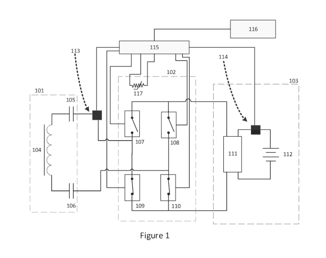
100281 FIG. 1 schematically illustrates a high-level circuit
implementation
of a safety enhanced magnetic resonant induction system.
100291 FIG. 2 schematically illustrates a generic safety circuit for a
voltage
source with reactive load.
100301 FIG. 3 schematically illustrates a generic safety circuit for a
current
source with reactive load.
100311 FIG. 4A schematically illustrates switch-based synchronous
rectification of an alternating voltage source with a complex load impedance.
100321 FIG. 4B schematically illustrates switch-based synchronous
rectification of an alternating current source with a complex load impedance.
100331 FIG. 4C schematically illustrates switch-based synchronous
rectification of an alternating voltage source with a direct voltage load.
100341 FIG. 4D schematically illustrates switch-based synchronous
rectification of an alternating current source with a direct voltage load.
100351 FIG. 5A schematically illustrates passive rectification of an
alternating voltage source with an impedance load.
100361 FIG. SB schematically illustrates passive rectification of an
alternating current source with an impedance load.
[0037] FIG. SC schematically illustrates an alternate embodiment of
passive
rectification of an alternating current source with an impedance load.
100381 FIG. 6 schematically illustrates an alternate embodiment of
switch-
based synchronous rectification of an alternating current source with an
impedance load.
100391 FIG. 7A schematically illustrates a parallel-parallel resonant
induction circuit.
7
CA 03163694 2022-06-02
WO 2021/211177
PCT/US2020/067339
[0040] FIG. 7B schematically illustrates an unbalanced series-series
resonant induction circuit.
[00411 FIG. 7C schematically illustrates a hybrid parallel-unbalanced
series
resonant induction circuit.
[0042] FIG. 71) schematically illustrates a hybrid unbalanced series-
parallel
resonant induction circuit.
[00431 FIG. 7E schematically illustrates a hybrid parallel-balanced
series
resonant induction circuit.
[0044] FIG. 7F schematically illustrates a hybrid balanced series-
parallel
resonant induction circuit.
[0045] FIG. 7G schematically illustrates a balanced series-series
resonant
induction circuit.
[0046] FIG. 8 geometrically illustrates a coil for use in a magnetic
resonance
inductive power system.
[0047] FIG. 9 schematically illustrates an unbalanced circuit equivalent of
a
planar coil for use in a resonance inductive power system.
[00481 FIG. 10 schematically illustrates a balanced circuit equivalent
of a
planar coil for use in a resonance inductive power system.
[0049] FIG. II illustrates the parasitic electric fields for a resonance
inductive power system of an electric vehicle with an unbalanced resonant
network.
8
CA 03163694 2022-06-02
WO 2021/211177
PCT/US2020/067339
DETAILED DESCRIPTION OF ILLUSTRATIVE EMBODIMENTS
[0050] Exemplary embodiments of the invention will be described with
respect to the Figures. The current source safety circuit and associated
method
described herein may be understood more readily by reference to the following
detailed description taken in connection with the accompanying figures and
examples, which form a part of this disclosure. It is to be understood that
this
description is not limited to the specific products, methods, conditions or
parameters described and/or shown herein, and that the terminology used herein
is for the purpose of describing particular embodiments by way of example only
and is not intended to be limiting of any claimed subject matter. Similarly,
any
description as to a possible mechanism or mode of action or reason for
improvement is meant to be illustrative only, and the subject matter described
herein is not to be constrained by the correctness or incorrectness of any
such
suggested mechanism or mode of action or reason for improvement. Throughout
this text, it is recognized that the descriptions refer both to methods and
systems/software for implementing such methods.
[00511 A detailed description of illustrative embodiments will now be
described with reference to FIGS 1.-11, Although this description provides a
detailed example of possible implementations, it should be noted that these
details are intended to be exemplary and in no way delimit the scope of the
inventive subject matter,
[0052] In a wireless power transfer system using an open air-
transformer, the
resonant network (i.e., the primary/transmitter and secondary/receiver) used
for
magnetic/wireless charging produces an alternating current source for
rectification on the vehicle. Having a current source reverses most of the
conventions that are typical of voltage sources in household and industrial
use
scenarios for power supply. The key difference from these scenarios is that in
a.
voltage source short circuits are had. As a result, power conversion
topologies
are built with normally off devices to avoid a short. However, with current
sources the reverse is true: open circuits are had. This means that the
typical
rectification technologies are undesirable. A straight passive (e.g. diode-
based)
rectifier gives no protection. A conventional synchronous rectifier can
provide
protection but only as long as there is a reliable means of energizing the
devices
to turn them on,
9
CA 03163694 2022-06-02
WO 2021/211177
PCT/US2020/067339
[00531 FIG. 1 schematically illustrates a high-level schematic for a
direct
current battery charging circuit using magnetic induction resonance. The
resonant network 101 (aka the receiver or secondary) consists of an inductive
secondary coil 104 with balanced capacitances 105 and 106. The secondary coil
104 converts the magnetic field from the charging transmitter (not shown) into
an alternating current (AC) signal that series resonates with the balanced
capacitances 105 and 106 in the voltage domain. As will be explained below
with respect to FIGS. 7A-7G, the primary side of the resonant network may be
balanced or unbalanced. The AC signal from the resonant network 101 is then
rectified into a direct current (DC) signal at rectification stage 102. The
rectification stage 102 consists of a synchronous rectification circuit using
paired
normally open (NO) switches 107 and 108 and paired normally closed (NC)
switches 109 and 110. As will be explained below, the paired NC switches 109
and 110 function to shunt the secondary coil 104 in the event of a fault. The
DC
signal is passed to the conditioning circuitry 111. The output of the
conditioning
circuitry 111 is a conditioned DC signal used to charge the battery 112.
[00541 The rectifier controller 115 phase locks to the resonant network
current at the first current and voltage sensor 113 as a reference for
controlling
the timing of the rectifier switches 107-110 (e.g., with respect to detected
zero
crossings). The rectifier controller 115 (nominally a Field Programmable Gate
Array (TTGA) or conventional microcontroller) produces estimates of the
amplitude, frequency and instantaneous phase of the input AC waveform from
the secondary coil 104 via the first current and voltage sensor 113 whenever
the
AC waveform is of sufficient amplitude and the switching frequency is within
its
acquisition range. The rectifier controller 115 also monitors amplitude of the
output DC current waveform applied to the battery 112 via the second current
and voltage sensor 114.
10055] The vehicle charging processor 116 (nominally implemented as
software running on a microprocessor) handles communications with internal (to
the wireless power transfer (WPT) system) subsystems and external vehicle
systems via interfaces (e.g. a controller area network (CAN) bus) and can
command the actions of the rectifier controller 115. :For example, when
queried
by the vehicle charging processor 116,, the rectifier controller 115 may
report the
input AC signal amplitude, input AC signal frequency, DC output voltage and
CA 03163694 2022-06-02
WO 2021/211177
PCT/US2020/067339
current and the switching devices' temperature. lithe reported input switching
frequency is within the allowed closed range (e.g., 79 kHz to 90 kHz), the AC
root mean square (RMS) is above a threshold (e.g., 5 Amps), and there are no
detected faults, then the vehicle charging processor 116 may instruct the
rectifier
controller 115 to turn the upper pair of NO switches 107 and 108 and the lower
pair of NC switches 109 and 110 on-and-off at the appropriate zero-crossings
of
the input AC waveform to maximize the efficiency of rectification. The nominal
state is "startup" or "safe" where the upper pair of NO switches 107 and 108
are
open and the lower pair of NC switches 109 and 110 are closed. When the
secondary coil 104 is producing a positive signal, the first set of switches
107
and 109 are opened and the second set of switches 108 and 110 are closed.
When the signal from the secondary coil 104 inverts, the first set of switches
107
and 109 are closed and the second set of switches 108 and [10 are opened. This
sequence repeats, resulting in an output signal which is mathematically the
absolute value of the input AC signal.
[0056] If disabled by the vehicle charging processor 116, the rectifier
controller 115 holds the upper NO switch pair 107 and 108 off and the lower
INC
switch pair 109 and 110 on. Also, if an over-voltage, over-current fault
condition is detected at the current and voltage sensor 114 or an over-
temperature fault condition is detected at temperature sensor 117, the
rectifier
controller 115 holds the upper NO switch pair 107 and 108 Off and lower
switches NC pair 109 and 110 On to shunt the current from the secondary coil
104.
[0057] The rectifier controller 115 monitors the output DC voltage from
the
rectification stage 102 via current and voltage sensor 114. The rectifier
controller 115 also measures output DC current via current and voltage sensor
114 and reports the output DC current to the vehicle charging processor 116 so
that the system may compute the total power delivered to the battery 112. in
addition, the rectifier controller 115 may monitor the temperature sensor or
sensors (e.g. a therraistor or network of thermistors) 117 that measures the
temperature of the mounting plate of the rectifier's switching devices 107-
110.
This mounting-plate temperature represents the case temperature of the
switching devices 107-110, which is related to the power losses through the
switching devices 107-110.
11
CA 03163694 2022-06-02
WO 2021/211177
PCT/US2020/067339
[00581 When paired with a series-series resonant transmitter (not
shown), the
resonant network 101 is an AC current source. Any condition that open circuits
the resonant network 101 results in an unsafe condition, However, the
selection
of NO switches 107 and 108 and NC switches 109 and 110 for the synchronous
rectification stage 102 results in an inherently safe system. In the normal
condition, either incidentally or specifically controlled, the NC switches 109
and
110 may be closed to shunt the secondary coil 104, thus providing means for
shunting the AC current source of the resonant network 101. The NO switches
107 and 108 prevent shorting the output network 103, particularly the battery
112.
[0059] In the event of a fault, the battery 112 is disconnected from the
signal
conditioning circuitry 111, and the current flow out of the conditioning
circuitry
111 is reduced to zero while the current flow into the conditioning circuitry
111
does not change. This will cause the voltage across the conditioning circuitry
-15 111 and rectification stage 102 to increase at a rate proportional to
the rectified
current and impedance of the conditioning circuitry 111.
[00601 The rectifier controller 115 monitors the voltage and/or current
using
current and voltage sensor 114 to detect the disconnection of the battery 112.
In
the event of a fault, the rectifier controller -115 may respond by opening NO
switches 107 and 108 and closing NC switches 109 and 110. This acts to
disconnect the resonant network 101 from the conditioning circuitry 111 and
battery 112. Power transfer will stop immediately as the rectified current
flow
out of the rectification stage 102 to the conditioning circuitry 111 and
battery
112 will be interrupted by NO switches 107 and 108 and current flow out of the
resonant network 101 will be shunted through NC switches 109 and 110.
[00611 in the passive state, where there is no control power to operate
a
controller or to synchronously rectify, the NO switches 107 and 108 open the
output network 103 while the NC switches 109 and 110 shunt the resonant
network 101. This protects the charger, load and service personnel from
spurious energy picked up by the resonant network 101, whether the spurious
energy is accidental or malicious.
[0062] FIG. 2 schematically illustrates a generic safety circuit for a
voltage
source with reactive load. In FIG. 2, a generic voltage source supply
protection
solution is shown where the voltage source 201 and load 202 share a common
12
CA 03163694 2022-06-02
WO 2021/211177
PCT/US2020/067339
ground 203, The voltage source 201 provides a fixed voltage invariant of the
sourced current. The source current is set by the load impedance of load 202.
Current sensor 205 monitors the source current. lithe source current exceeds
an
allowable limit, the current sensor 205 provides a protection function by
triggering the normally open switch 204 to its open state. The normally open
switch 204 remains open until reset. Once the disconnect of normally open
switch. 204 is triggered, the voltage across and current flow thru the load
202 are
driven to zero. The Normally Open (NO) switch 204 and current sensor 205
shown here is merely one implementation option with various relays, circuit
breakers, and fuses in wide use. Virtually all power supply and distribution
networks operate with a voltage source and implement some sort of current
limiting scheme using some form of breaker or fuse as illustrated in FIG. 2.
It
will be appreciated that in a voltage source power system, open circuits are
good
and short circuits are bad.
[00631 The current source supply depicted in FIG. 3 is a much less common
implementation. A constant current supply requires a mirror of all the best
practices in safety protection of the more common voltage source supply. It
will
be appreciated that in a current source power system, unlike a voltage source
power system, open circuits are bad and shunts (intentional short circuits)
are
good practice. Hence, different embodiments of the safety circuit described
herein should be considered based on whether the power supply is a current
source power system or a voltage source power system.
[0064] FIG. 3 schematically illustrates a generic safety circuit for a
current
source with reactive load. The current source 301 supplies the electric
current to
the reactive load 302 independent of the voltage across it. In this example,
all
circuit paths share a common ground 303. The current source 301 provides a
fixed current invariant of the voltage current.
[0065] To provide a current shunt and isolation of the load from the
source
(and vice-versa), a voltage-sensitive disconnect is placed in parallel with
the
reactive load 302, The Normally Closed (NC) switch shunt 304 and voltage
sensor 305 shown in FIG, 3 is merely one implementation option of shunting
means with various switches, relays, circuit breakers, and fuses in wide use.
Once the NC switch shunt 304 is triggered by the voltage sensor 305, the NC
13
CA 03163694 2022-06-02
WO 2021/211177
PCT/US2020/067339
switch shunt 304 is opened to drive the voltage and current flow through the
reactive load 302 to zero.
[00661 FIGS. 4A-4D all illustrate alternative embodiments of the safety
rectification circuit and additional subsystems needed for wireless power
transfer.
[0067] FIG. 4A schematically illustrates switch-based synchronous
rectification of an alternating voltage source with a complex load impedance.
In
particular, FIG. 4A illustrates a conventional alternating current (AC)
voltage
source and a safety-enhanced synchronous rectification circuit to create a
direct
current (DC) voltage source. The AC voltage source 401 is synchronously
rectified by the set of normally open (NO) switches 402, 403, 404, and 405.
The
power conditioning network 406 provides filtering of the rectified DC voltage
into a DC voltage source for the load 407. In the event of a fault, the NO
switches fail open, disconnecting and protecting the load 407 from AC voltage
source 401.
[0068] FIG. 4B schematically illustrates switch-based synchronous
rectification of an alternating current source with a complex load impedance
in a
sample embodiment. In particular, FIG. 413 illustrates an AC current source
and
a safety-enhanced synchronous rectification circuit to create a DC current
source. The AC current source 410 is synchronously rectified by the set of NO
switches 403 and 404 and normally closed (INC) switches 408 and 409, The
power conditioning network 406 provides filtering of the rectified current
into a
DC current source for the load 407. The A.0 current source 410 necessitates
the
set of NC switches 408 and 409 to open to provide means for shunting current
in
the event of a fault. In the faulted condition, the closed switches 408 and
409
isolate the load 407 from the AC current source 410 to prevent any back feed
of
power.
[0069] FIG. 4C schematically illustrates switch-based synchronous
rectification of an alternating voltage source with a direct voltage load. In
particular, FIG. 4C illustrates an. AC voltage source and a safety-enhanced
synchronous rectification circuit to create a DC voltage source for charging a
battery. The AC voltage source 401 is synchronously rectified by the set of NO
switches 402, 403, 404, and 405. The power conditioning network 406 provides
filtering of the rectified voltage into a DC: voltage source for the power
14
CA 03163694 2022-06-02
WO 2021/211177
PCT/US2020/067339
conversion stage 411, The power conversion stage 411 adapts the DC voltage
source to the required voltage for charging the battery 412.
[00701 FIG. 4D schematically illustrates switch-based synchronous
rectification of an alternating current source with a direct voltage load in a
sample embodiment. In particular, FIG. 41) illustrates an AC current source
and
a safety-enhanced synchronous rectification circuit to create a DC voltage
source
for charging a battery. The AC current source 410 is synchronously rectified
by
the set of NO switches 402 and 403 and NC switches 408 and 409. The power
conditioning network 406 provides filtering of the rectified current into a DC
current source for the battery 412. The AC current source 410 necessitates the
set of NC switches 408 and 409 to provide means for shunting current in the
event of a fault. However, as the system is powered by a current source, the
power conversion stage 411 of FIG. 4C is not needed for battery charging.
[00711 FIG. 5A schematically illustrates passive rectification of an
alternating voltage source with an impedance load. In particular, FIG. 5A
shows schematically a conventional passive full-wave rectifier circuit for an
AC
voltage source 501. The diodes 502, 503, 504, and 505 act as one-way gates,
creating a full-wave rectification of the A.0 signal. The power conditioning
stage 506 serves to smooth the rectifier voltage output applied to the load
507,
allowing the load 507 to be charged.
[00721 Like all diode circuits, reverse recovery time and voltage drop
in the
forward bias condition impact the efficiency of the rectification circuit. The
passive rectifier circuit does not need a controller stage. However, in the
event
of a fault, the AC voltage source 501 is still connected to the load 507 via
the
power conditioning stage 506 exposing the load 507 to voltage source faults
(and
vice-versa).
[00731 FIG. 5B schematically illustrates passive rectification of an
alternating current source with an impedance load in a sample embodiment. In
particular, FIG. 5B shows a hybrid embodiment of a safety-enhanced circuit for
rectification of an AC current source 508. The full-bridge passive rectifier
diodes 502, 503, 510, and 512 are supplemented by the normally closed (NC)
switches 509 and 511. The diodes 502, 503, 510, and 512 act as one-way gates,
creating a full-wave rectification. The NC switches 509 and 511 act as means
for
shunting in the case of a failure, preventing overvoltage damage to the AC
CA 03163694 2022-06-02
WO 2021/211177
PCT/US2020/067339
current source 508 and across the diodes 502, 503, 510, and 512. The power
conditioning stage 506 serves to smooth the rectifier voltage output applied
to
the load 507, allowing the load 507 to be charged.
[0074] Like all diode-based rectification circuits, reverse recovery
time and
voltage drop in the forward bias condition impact the efficiency of the
rectification circuit. The passive rectifier circuit does not need a
controller stage,
but a controller (e.g., rectifier controller 115) is needed to command the NC
switches 509 and 511.
10075] FIG. SC schematically illustrates an alternate passive
rectification of
an alternating current source with an impedance load in a sample embodiment.
In particular, FIG. SC shows an alternative, semi-passive embodiment of a full-
wave safety-enhanced rectifier circuit for an AC current source 508. The
diodes
502, 503, 510, and 512 act as one-way gates, creating a full-wave
rectification.
The power conditioning stage 506 serves to smooth the rectifier voltage output
applied to the load 507, allowing the load 507 to be charged. In this
embodiment, a normally closed (NC) shunt switch 513 is placed in the circuit.
In the event of a fault or command option, the shunt switch 513 shunts the
current in the rectifier circuit, preventing damage to the power conditioning
stage 506 and the load 507.
[0076] This embodiment is a cheaper implementation with simpler controls.
However, it is less efficient. Additionally, it places a high dVldt across the
isolated control boundary for shunt switch 513. Like all diode-based
rectification circuits, reverse recovery time and voltage drop in the forward
bias
condition impact the efficiency of the rectification circuit.
[0077] FIG. 6 schematically illustrates an alternate switch-based
synchronous rectification of an alternating current source with an impedance
load in a sample embodiment, In particular, FIG. 6 illustrates an alternative
safety circuit for active rectification of an AC current source 601. The power
conditioning stage 606 serves to smooth the rectifier voltage output applied
to
the load 607 to be charged. The full-wave rectification is accomplished by
alternately switching at zero crossing of the sinusoidal output of the AC
current
source 601. A normally closed (NC) safety switch 608 is installed between the
Normally Open (NO) upper rectification switches 602 and 604 and lower
Normally Open (N-0) rectification switches 603 and 605 that provides, in the
16
CA 03163694 2022-06-02
WO 2021/211177
PCT/US2020/067339
event of a fault or commanded option, a means for shunting the current in the
rectifier circuit, preventing damage to the power conditioning stage 606 and
the
load 607.
[0078] In a fault condition or loss of rectification control, the NO
rectification switches 602, 603, 604, and 605 fail (or are commanded) to the
Open state while the NC safety switch 608 fails to the Closed state. Current
is
thus shunted back to the AC current source 601 while the load is isolated by
the
NC safety switch 608. This embodiment reduces the demand for normally closed
(NC) switches at the expense of an additional switch 608.
[0079] For resonant induction wireless charging, there are four potential
two
pole networks. There is the parallel-parallel resonant network (PPRN) and
series-series resonant network (SSRN). Due to the galvanic isolation, it is
also
possible to create a parallel-series resonant network (PSRN) and a series-
parallel
resonant network (SPRN), The PPRN, PSRN and SPRN all behave as AC
Voltage Controlled Voltage Sources (VCVS) when the load impedance is large
compared to the network impedance and all behave as AC Voltage Controlled
Current Sources (VCCS) when the load impedance is small compared to the
network impedance. On the other hand, the SSRN behaves as a VCCS for all
load impedances. A constant voltage load, e.g. a battery, appears as a
variable
load impedance as the power level is varied. At low powers, a battery will
appear as a high impedance load and at high powers it will appear as low
impedance. At high power, all four resonant networks will behave as a VCCS.
[0080] When operating as a .VCCS, the PPRN has a'fran.sconductance (G)
of k / (w*L) in units of Amperes per Volt, where k is the magnetic coupling
coefficient of the primary and secondary inductors in the range of zero to one
and is unitless, w is the resonant frequency of the network in radians per
second,
and L is the geometric mean of the primary and secondary inductors in Henrys.
When operating as a VCCS, the PSRN. SPRN and SSRN have a G of 1 /
(w*L*k). This means for a fixed G then then the inductor of the PPRN has an
inductor smaller by k2 and the capacitor of the PPRN is larger by 1(2. This is
undesirable as the capacitor is the much more expensive component.
[0081] The resonant network resonates an amount of power S that is
proportional to P/k where P is the power through the network. For typical
values
of k (e.g., 0.05-0.2), S will be 5 to twenty times higher than P. In parallel
17
CA 03163694 2022-06-02
WO 2021/211177
PCT/US2020/067339
resonant branches, the resonant power is seen as current through the
capacitive
and inductive elements. In series resonant branches, the resonant power is
seen
as additional voltage across the capacitive and inductive elements. For
example,
in a 500V and 1.25A system with a k of 0.1, in a parallel resonance there
would
be 125A/0.1 or 1.,250A resonating in the inductor and capacitor, while in a
series
resonance there would be 500V/0.1 or 5,000V resonating across the inductor and
capacitor. The series resonance case is preferred as higher voltages require
additional isolation while higher currents require additional conductors and
so
higher voltages allow for a lighter and more compact product.
[0082] With these considerations in mind, each of the PSRN. SPRN and
SSRN may have both a balanced and unbalanced topology. The PPRN only has
a balanced topology. Each of these topologies is illustrated in FIGS. 7A-7G.
[0083] FIG. 7A schematically illustrates a balanced PPRN circuit in a
sample embodiment. This resonant network comprises a ground inductive coil
701, a ground parallel resonant capacitor 703, a vehicle inductive coil 702,
and a
vehicle parallel resonant capacitor 704.
[008431 FIG 713 schematically illustrates an unbalanced SSRN circuit in a
sample embodiment. This resonant network comprises a ground inductive coil
701, a ground series resonant capacitor 705, a vehicle inductive coil 702, and
a
vehicle series resonant capacitor 706.
[00851 FIG 7C schematically illustrates an unbalanced PSRN circuit in a
sample embodiment. This resonant network comprises a ground inductive coil
701, a ground parallel resonant capacitor 707, a vehicle inductive coil 702,
and a
vehicle series resonant capacitor 708.
[00861 FIG. 7D schematically illustrates an unbalanced SPRN circuit in a
sample embodiment. This resonant network comprises a ground inductive coil
701, a ground series resonant capacitor 709, a vehicle inductive coil 702, and
a
vehicle parallel resonant capacitor 710.
[00871 FIG. 7E schematically illustrates a balanced PSRN circuit in a
sample embodiment. This resonant network comprises a ground inductive coil
701, a ground parallel resonant capacitor 711, a vehicle inductive coil 702,
and a
pair of vehicle series resonant capacitors 712 and 713.
[0088] FIG. 7F schematically illustrates a balanced SPRN circuit in a
sample embodiment. This resonant network coMprises a ground inductive coil
18
CA 03163694 2022-06-02
WO 2021/211177
PCT/US2020/067339
701, a pair of ground series resonant capacitors 714 and 715, a vehicle
inductive
coil 702, and a vehicle parallel resonant capacitor 716.
[00891 FIG. 7G schematically illustrates a balanced SSRN circuit in a
sample embodiment. This resonant network comprises a ground inductive coil
701, a pair of ground series resonant capacitors 717 and 718, a vehicle
inductive
coil 702, and a pair of vehicle series resonant capacitors 719 and 720.
[00901 FIG. 8 geometrically illustrates a planar coil 801 for use as a
primary
coil in a magnetic resonance inductive power system in a sample embodiment.
While shown as a squared coil, other geometries (e.g. classic round coil or
rectangular) are also possible. The coil winding 803 is disposed on an
insulative
substrate 805 and may include discrete conductive ribbons (e.g., a printed
circuit
board), insulated wire strands (e.g., Litz wire), or the like. Vias 802 and
804
permit connectivity with another coil on the opposite side of the insulative
substrate 805.
[009I1 FIG. 9 schematically illustrates an unbalanced circuit equivalent of
planar coil 801 for use in a series resonant network 901 in a sample
embodiment.
The series resonant network 901 is a transmitter. The terminals 906 and 907 of
the network are connected to an inverter. The resonant capacitor 905 has a
high
voltage high frequency voltage across it as the series resonant network 901 is
resonated. This same voltage is seen across the inductor 903. The first
terminal
904 of the inductor 903 is effectively held at ground potential. The second
terminal 902 of the inductor is exposed to the full voltage of the resonant
capacitor 905 relative to ground. In other words, the voltage of the inductor
903
has a common mode voltage relative to ground of one half the voltage across
the
resonant capacitor 905, which makes the inductor 903 a capacitive
electromagnetic interference (EMT) radiator. In this configuration, techniques
are desired for mitigating the EMI radiation, as noted below with respect to
FIG.
11.
[00921 FIG. 10 schematically illustrates a balanced circuit equivalent
of
planar coil 801 for use in a series resonant network 1001 in a sample
embodiment. The series resonant network 1001 is also a transmitter. The
terminals 1007 and 1008 of the network are connected to an inverter. The
capacitors 1005 and 1006 have a high voltage high frequency voltage across
them as the series resonant network 1001 is resonated. The sum of their
voltages
19
CA 03163694 2022-06-02
WO 2021/211177
PCT/US2020/067339
is seen across the inductor 1003, However, as the series resonant network 1001
is balanced, the midpoint of the inductor 1003 between terminals 1002 and 1004
is virtually ground. So, while there is a differential voltage across the
inductor
1003, there is no high frequency common mode voltage to ground. The inductor
1003 does not capacitively radiate EMI, and no mechanism is required for
handling the EMI.
[00931 FIG. 11 illustrates the parasitic electric fields for a resonance
inductive power system of an electric vehicle 1101 with an unbalanced resonant
network leading to EMI radiation in a sample embodiment. Electric vehicles
1101 have marginal conductance between the chassis 1106 and ground 1108
through the tires 1102. The admittance, at high frequencies, between the
chassis
1106 and ground 1108 is dominated by the capacitance between the chassis 1106
and ground 1108. Common mode capacitive EMI generated by the transmitter
1104 or the receiver 1103 must be minimized as the electric field 1105
developed in the gap 1107 between the chassis 1106 and ground 1108 will
energize the capacitance and introduce a voltage on the chassis 1106. At a
minimum, this capacitive coupling can extend an EMI problem and at worst it
can present a shock hazard.
[0094] The chassis voltage may be reduced by the addition of conductive
path(s) to ground that function as means for grounding the EMI while charging
is underway. The already conductive materials (carbon black) of tires may be
enhanced with the addition of lower resistance conductive vias through the
tire
material. Deployment of a grounding cable or wire 'tail' could also be used to
mitigate chassis voltages during charging. Chassis voltage also may be
mitigated by the addition of a circuit powered by the wireless charging system
or
vehicle battery system that cancels out-of-phase voltages during charging.
[0095] It will be appreciated by those skilled in the art that the
embodiments
described herein provide various means for shunting the direct current
waveform
in the event of a fault so as to minimize the possibility of electric shock
while
charging. The techniques may be used for balanced or unbalanced resonant
network topologies. The rectification circuitry may include diodes and/or
switches in configurations designed to shunt the power in the event of a
fault,
which leads to increased safety during the charging process, particularly for
high
power transfer applications such as the charging of electric vehicles.
CA 03163694 2022-06-02
WO 2021/211177
PCT/US2020/067339
[0096] As discussed herein, the logic, commands, or instructions that
implement aspects of the methods described herein may be provided in a
computing system including any number of form factors for the cornputing
system such as desktop or notebook personal computers, mobile devices such as
tablets, netbooks, and smartphones, client terminals and server-hosted machine
instances, and the like. Another embodiment discussed herein includes the
incorporation of the techniques discussed herein into other forms, including
into
other forms of programmed logic, hardware configurations, or specialized
components or modules, including an apparatus with respective means to
perform the functions of such techniques. The respective algorithms used to
implement the functions of such techniques may include a sequence of some or
all of the electronic operations described herein, or other aspects depicted
in the
accompanying drawings and detailed description below. Such systems and
computer-readable media including instructions for implementing the methods
described herein also constitute sample embodiments.
[0097] The monitoring and control functions described herein may be
implemented in software in one embodiment. The software may consist of
computer executable instructions stored on computer readable media or
computer readable storage device such as one or more non-transitory memories
or other type of hardware-based storage devices, either local or networked.
Further, such functions correspond to modules, which may be software,
hardware, firmware, or any combination thereof. Multiple functions may be
performed in one or more modules as desired, and the embodiments described
are merely examples. The software may be executed on a digital signal
processor, ASIC, microprocessor, or other type of processor operating on a
computer system, such as a personal computer, server, or other computer
system,
turning such computer system into a specifically programmed machine.
[0098] Examples, as described herein, may include, or may operate on,
processors, logic, or a number of components, modules, or mechanisms (herein
"modules"). Modules are tangible entities (e.g., hardware) capable of
performing specified operations and may be configured or arranged in a certain
manner. In an example, circuits may be arranged (e.g., internally or with
respect
to external entities such as other circuits) in a specified manner as a
module. In
an example, the whole or part of one or more computer systems (e.g., a
21
CA 03163694 2022-06-02
WO 2021/211177
PCT/US2020/067339
standalone, client or server computer system) or one or more hardware
processors may be configured by firmware or software (e.g., instructions, an
application portion, or an application) as a module that operates to perform
specified operations. In an example, the software may reside on a machine
readable medium. The software, when executed by the underlying hardware of
the module, causes the hardware to perform the specified operations.
100991 Accordingly, the term "module" is understood to encompass a
tangible hardware and/or software entity, be that an entity that is physically
constructed, specifically configured (e.g., hardwired), or temporarily (e.g.,
transitorily) configured (e.g., programmed) to operate in a specified manner
or to
perform part or all of any operation described herein. Considering examples in
which modules are temporarily configured, each of the modules need not be
instantiated at any one moment in time. For example, where the modules
comprise a general-purpose hardware processor configured using software, the
general-purpose hardware processor may be configured as respective different
modules at different times. Software may accordingly configure a hardware
processor, for example, to constitute a particular module at one instance of
time
and to constitute a different module at a different instance of time.
[001001 Those skilled in the art will appreciate that the topology and
circuit
implementation methodology described herein enables effective realization as a
single application specific integrated circuit. Further, while the disclosure
contained herein pertains to the provision of electrical power to vehicles, it
should be understood that this is only one of many possible applications, and
other embodiments including non-vehicular applications are possible. For
example, those skilled in the art will appreciate that there are numerous
applications of providing a current source safety circuit in non-vehicle
inductive
charging applications such as portable consumer electronic device chargers,
such
as those (e.g., PowerMatrm) used to charge toothbrushes, cellular telephones,
and other devices. Accordingly, these and other such applications are included
within the scope of the following claims.
22