Note: Descriptions are shown in the official language in which they were submitted.
CA 03164318 2022-06-10
WO 2021/118971 PCT/US2020/063739
Random Access Sensor
CROSS REFERENCE TO RELATED CASES
[00011 This application claims priority to co-pending Provisional U.S.
Application No.
62/947,579, entitled "Random Access Sensor" filed December 13, 2019, and Non-
Provisional U.S. Application No. 16/952,418, entitled "Random Access Sensor"
filed.
November 19, 2020.
TECHNOLOGICAL FIELD
[0002] Various aspects of the disclosure relate to a randomly addressable
sensor.
BACKGROUND
[0003] CMOS sensors are finding widespread use in image capturing
environments. Pixel
arrays in a 0,40S sensor may be exposed using different techniques including a
global
shutter, in which all pixels are exposed simultaneously for the same exposure
interval,
and a rolling shutter, in which the pixels are exposed sequentially, often
line-by-line, in
photography and some video applications, rolling shutters can unnaturally skew
images
by incorporating movement artifacts. In other applications, the ability to
quickly capture
and read out captured data is of higher importance.
SUMMARY
[0004] The following summary presents a simplified summary of certain
features. The
summary is not an extensive overview and is not intended to identify key or
critical
elements.
[0005] Disclosed is a circuit, e.g., a CMOS sensor, with individually
addressable transfer
transistors and individually addressable reset transistors. Through the
in.dividually
addressable transistors, pixels within different regions of interest, of the
same or
different size and/or the same or different exposure times, can be efficiently
processed.
Different regions of interest may be exposed concurrently and read out
independently.
As such, systems, apparatuses, and methods are described for a random access
CMOS
sensor. The CMOS sensor may include photodiodes, floating diffusion nodes, and
transfer transistors connecting the photodiodes to the floating diffusion
nodes. The
1
SUBSTITUTE SHEET (RULE 26)
CA 03164318 2022-06-10
WO 2021/118971 PCT/US2020/063739
transfer transistors may be selectable by two or more transfer select signals.
The transfer
select signals may be combined by one or more transistors connected to control
the
operation of the transfer transistors. By using two or more transfer select
signals, the
transfer transistors may be individually addressed. The output of the CMOS
sensor may
include a source-follower output. The CMOS sensor may include reset
transistors and/or
selection transistors in which the transistors may be controlled by two or
more select
signals. Using combinations of select signals, the related transistors may be
individually
addressed. The CMOS sensor may include one or more regions of interest (ROIs)
in
which each ROI is handled by one or more sets of control circuitry.
[0006] Accordingly, the present disclosure includes CMOS sensors, pixels,
and/or circuits,
including circuits comprising a first transfer transistor connecting a
photodiode to a
floating diffusion node, wherein the first transfer transistor is individually
selectable by
a combination of: (i) a first transfer select input, and (ii) a second
transfer select input;
an output transistor in a source-follower configuration with a gate connected
to the
floating diffusion node; and, a selection transistor connecting the output of
the output
transistor. In some embodiments, the circuit further comprises a first
transfer selection
transistor having a gate terminal connected to (i) the first transfer select
input, or (ii) the
second transfer select input, the first transfer selection transistor being
connected
between: (1) the gate terminal of the first transfer transistor, and (2) the
other of: (a) the
first transfer select input or (b) the second transfer select input,
[0007] In one or more aspects, the circuit further comprises an
individually addressable first
reset select input; an individually addressable second reset select input; a
reset transistor
connected between one or more potentials and the floating diffusion node; and,
a first
reset selection transistor having a gate terminal connected to: (i) the first
reset select
input, or (ii) the second reset select input, the first reset selection
transistor otherwise
being connected between (I) the gate terminal of the reset transistor, and (2)
the other
of: (a) the first reset select input, or (b) the second reset select input.
The circuit may
also comprise a second transfer selection transistor, wherein the second
transfer
selection transistor includes a gate terminal connected to a complement of (i)
the first
transfer select input or (ii) the second transfer select input, the second
transfer selection
transistor otherwise being connected between: (1) the gate terminal of the
first transfer
SUBSTITUTE SHEET (RULE 26)
CA 03164318 2022-06-10
WO 2021/118971 PCT/US2020/063739
transistor, and (2) one or more potentials.
[0008] in some embodiments, the circuit further comprises a second reset
selection transistor,
wherein the second reset selection transistor has a gate terminal connected to
a
complement of one of (i) the first reset select input, or (ii) the second
reset select input,
the second reset selection transistor otherwise being connected between: (1)
the gate
terminal of the reset transistor, and (2) one or more of the potentials.
[0009] Also disclosed is a circuit that further comprises a transfer
selection transistor having a
gate terminal connected to one of (i) the first transfer select input, or (ii)
the second
transfer select input, the transfer selection transistor otherwise being
connected
between: (1) the gate terminal of the first transfer transistor, and (2) the
other of (a) the
first transfer select input or (b) the second transfer select input.
[0010] The circuits may further comprise an individually addressable first
reset select input; an
individually addressable second reset select input; a reset transistor
connected between
at least one potential and the floating diffusion node; and, a reset selection
transistor
having a gate terminal connected to one of (i) the first reset select input,
or (ii) the second
reset select input, the reset selection transistor being otherwise connected
between: (I)
the gate terminal of the reset transistor, and (2) the other of (a) the first
reset select input,
and (h) the second reset select input. In embodiments, the circuit comprises
at least one
anti-blooming transistor. In one or more embodiments, the circuit comprises at
least one
transfer selection control circuit configured to (i) individually address the
first transfer
select inputs, and (ii) individually address the second transfer select inputs
[0011] The circuits herein may be used in, for example, a spectrometer
system, and thus also
disclosed are spectrometers comprising the circuits described herein.
[0012] Also disclosed are CMOS sensors, the CMOS sensors comprising at
least one source
follower output; at least one transfer selection control circuit configured to
control (i)
individually addressable first transfer select inputs, and (ii) individually
addressable
second transfer select inputs; an array of pixels comprising: (a) photodiodes,
(h) floating
diffusion nodes; (c) transfer transistors connecting the photodiodes to the
floating
diffusion nodes, wherein the transfer transistors are individually selectable
by the
combination of the first transfer select inputs and second transfer select
inputs and (d)
output transistors in a source-follower configuration connecting the floating
diffusion
3
SUBSTITUTE SHEET (RULE 26)
CA 03164318 2022-06-10
WO 2021/118971 PCT/US2020/063739
nodes to output nodes; and, a controller configured to control the at least
one transfer
selection control circuit to expose: (i) a first pixel of the array of pixels
for a first length
of time, and (ii) a second pixel of the array of pixels for a second length of
time, the
second length of time being independent of the first length of time. In some
embodiments, the first length of time is different from the second length of
time; and/or
while in some embodiments, the first length of time and the second length of
time
commence at different times.
[0013] The CMOS sensor may further comprise a multiplexer; and, a plurality
of reading
circuits; wherein: a first reading circuit is connected, during a first
reading time, via the
multiplexer to read a value on a first source-follower output, and, a second
reading
circuit is connected, during a second reading time, via the multiplexer, to
read a value
on a second source-follower output. In embodiments, the second reading time is
independent of the first reading time.
[0014] It can thus be understood that the disclosed CMOS sensor can include
embodiments
wherein a first pixel and a second pixel are in a first row, wherein at least
the first pixel
is exposed for a first exposure time, and wherein at least the second pixel is
exposed for
a second exposure time, the second exposure time being independent of and/or
different
from the first exposure time. In some embodiments, a first pixel and a second
pixel are
in a first column, wherein at least the first pixel is exposed for a first
exposure time, and
wherein at least the second pixel is exposed for a second exposure time, the
second
exposure time being independent of and/or different from the first exposure
time, In
some CMOS sensors, the photodi odes are arranged between the transfer
transistors and
a light source, and in some systems, the light source is a light source of a
spectrometer.
Those of ordinary skill will thus recognize that the disclosed methods and
systems apply
to light sources that emit coherent and non-coherent light, and thus the
sensor(s) may
be monochromatic or chromatic, and the applications for the sensors may
include, but
are not limited to, sensing applications, imaging applications, and others.
[0015] Also disclosed is a CMOS sensor comprising at least one photodiode;
at least one
floating diffusion node; at least one output node; at least one individually
addressable
first transfer select input; at least one individually addressable second
transfer select
input; at least one transfer transistor connecting a first photodiode to a
first floating
4
SUBSTITUTE SHEET (RULE 26)
CA 03164318 2022-06-10
WO 2021/118971 PCT/US2020/063739
diffusion node, wherein a first transfer transistor is individually selectable
by the
combination of: (i) one of the first transfer select inputs, and (ii) one of
the second
transfer select inputs; and, at least one output transistor in a source-
follower
configuration connecting the at least one first floating diffusion node to the
at least one
output node. The CMOS sensor may further comprise at least a first transfer
selection
transistor having a gate terminal connected to: (i) one of the first transfer
select inputs,
or (ii) one of the second transfer select inputs, the first transfer selection
transistor
otherwise being connected between (I) the gate terminal of the at least one
first transfer
transistor, and (2) the other of: (a) the first transfer select input, or (b)
the second transfer
select input. The CMOS sensor may further comprise at least one individually
addressable first reset select input; at least one individually addressable
second reset
select input; at least one reset transistor connected between one or more
potentials and
the floating diffusion nodes; and at least a first reset selection transistor
having a gate
terminal connected to: (i) one of the first reset select inputs, or (ii) one
of the second
reset select inputs, the first reset selection transistor otherwise being
connected between
(1) the gate terminal of one of the reset transistors, and (2) the other of
(a) the first reset
select input, or (b) the second reset select input.
[0016] The disclosed CMOS sensors may further comprise a second transfer
selection
transistor, the second transfer selection transistor having a gate terminal
connected to a
complement of (i) one of the first transfer select inputs or (ii) one of the
second transfer
select inputs, the second transfer selection transistor otherwise being
connected between
(i) the gate terminal of the first transfer transistor, and (ii) one or more
potentials. In
embodiment, the CMOS sensor further comprises a second reset selection
transistor,
wherein the second reset selection transistor has a gate terminal connected to
a
complement of one of: (i) the first reset select input, or (ii) the second
reset select input,
the second reset selection transistor otherwise being connected between (i)
the gate
terminal of the first reset transistor, and (ii) one or more of the
potentials.
[0017] The CMOS sensor can further comprise at least a first transfer
selection transistor
having a gate terminal connected to one of (i) the first transfer select
input, or (ii) the
second transfer select input, the first transfer selection transistor
otherwise being
connected between (i) the gate terminal of a first transfer transistor, and
(ii) the other of
SUBSTITUTE SHEET (RULE 26)
CA 03164318 2022-06-10
WO 2021/118971 PCT/US2020/063739
(a) the first transfer select input or (b) the second transfer select input.
The CMOS
sensor, in embodiments, may further include at least one transfer selection
transistor,
wherein a first transfer selection transistor is connected in a source-
follower
configuration between a first photodiode and a first floating diffusion node.
In some
embodiments, the CMOS sensor further comprises at least one individually
addressable
first reset select input; at least one individually addressable second reset
select input; at
least one reset transistor connected between at least one potential and the
floating
diffusion nodes; and at least one reset selection transistor, a first reset
selection transistor
having a gate terminal connected to one of: (i) the first reset select input,
or (ii) the
second reset select input, the first reset selection transistors being
otherwise connected
between (I) the gate terminal of one of the reset transistors, and (2) the
other of (a) the
first reset select input, and (b) the second reset select input,
[0018] In some embodiments, the CMOS sensor further comprises at least one
transfer
selection control circuit configured to (i) individually address the first
transfer select
inputs, and (ii) individually address the second transfer select inputs.
[0019] In one or more embodiments, the CMOS sensor includes at least one
anti-blooming
transistor, The CMOS sensor can be utilized in a spectrometer system, and thus
the
present disclosure includes spectrometer systems that utilize a CMOS sensor as
disclosed,
[0020] Also disclosed is a CMOS sensor comprising at least one output; at
least one transfer
selection control circuit configured to control (i) individually addressable
first transfer
select inputs, and (ii) individually addressable second transfer select
inputs; an array of
pixels comprising: (a) photodiodes; (b) floating diffusion nodes; (c) transfer
transistors
connecting the photodiodes to the floating diffusion nodes; wherein the
transfer
transistors are individually selectable by the combination of the first
transfer select input
and second transfer select inputs; and, (d) output transistors in a source-
follower
configuration connecting the floating diffusion nodes to the at least one
output; and a
controller configured to control the at least one transfer selection control
circuit to
expose:(1) a first pixel of the array of pixels for a first length of time,
and, (2) a second
pixel of the array of pixels for a second length of time, the second length of
time being
independent of the first length of time. In some embodiments, the first length
of time is
6
SUBSTITUTE SHEET (RULE 26)
CA 03164318 2022-06-10
WO 2021/118971 PCT/US2020/063739
different from the second length of time, and/or the first length of time and
the second
length of time commence at different times.
[0021] In one or more embodiments, the CMOS sensor further comprises a
multiplexer; and a
plurality of reading circuits (e.g., plurality of single analog-to-digital
converter
channels), wherein: a first reading circuit is connected, during a first
reading time, via
the multiplexer to read a value on a first source-follower output, and a
second reading
circuit is connected, during a second reading time, via the multiplexer to
read a value
on a second source-follower output. The second reading time can be independent
of the
first reading time.
[0022] In some embodiments, a first pixel and a second pixel are in a first
row, wherein at least
the first pixel is exposed for a first exposure time, and wherein at least the
second pixel
is exposed for a second exposure time, the second exposure time being
independent of
the first exposure time. The first pixel and/or the second pixel can be in a
first column,
wherein at least the first pixel is exposed for a first exposure time, and at
least the second
pixel is exposed for a second exposure time, the second exposure time being
independent of the first exposure time. in embodiments, the photodiodes are
arranged
between the transfer transistors and a light source, where in some
embodiments, light
from the light source is modified by the optical components of a spectrometer.
These
and other features and advantages are described in greater detail below.
BRIEF DESCRIPTION OF HIE SEVERAL VIEWS OF THE DRAWINGS
[0023] Some features are shown by way of example, and not by limitation, in
the accompanying
drawings, In the drawings, like numerals reference similar elements.
[0024] Figure 1 shows a circuit/pixel of a CMOS sensor with three
transistors.
[0025] Figure 2 shows a circuit/pixel of a CMOS sensor with four
transistors.
[0026] Figure 3 shows a circuit/pixel of a CMOS sensor with an anti-
blooming transistor.
[0027] Figure 4 shows a circuit/pixel of a CMOS sensor with two transfer
select signals and an
optional anti-blooming transistor.
[0028] Figure 5 shows one example timing diagram of a CMOS sensor with two
transfer select
signals.
[0029] Figure 6 shows an example logic table of the operation of a transfer
transistor using two
transfer select signals.
SUBSTITUTE SHEET (RULE 26)
CA 03164318 2022-06-10
WO 2021/118971 PCT/US2020/063739
[0030] Figure 7 shows a circuit/pixel of a CMOS sensor with two transfer
select signals and
two reset select signals and an optional anti-blooming transistor.
[0031] Figure 8 shows an example timing diagram of a CMOS sensor with two
transfer select
signals and two reset select signals.
[0032] Figure 9A shows an example logic table for the operation of a reset
transistor using two
reset select signals. Figure 9B shows an example logic table for the operation
of a
transfer transistor using two transfer select signals.
[0033] Figure 10A shows a circuit/pixel of a CMOS sensor with separate
transistors controlling
the operation of a transfer transistor and a reset transistor. Figure 10B
shows an
alternative view of the circuit/pixel of Figure 10A with additional
annotations.
[0031] Figure 11 shows one example timing diagram of the CMOS sensor of
Figure 10B.
[0035] Figure 12A shows an example logic table for the operation of the
reset transistor of
Figure 10B, Figure 12B shows an example logic table for the operation of the
transfer
transistor of Figure 10B,
[0036] Figure 13A shows a circuit/pixel with a transfer transistor
controlled by two transistors.
Figure 1313 shows an alternative view of the circuit/pixel of Figure 13A with
additional
annotations.
[0037] Figure 14 shows an example timing diagram. for the pixel of Figure
13B.
[0038] Figure 15A shows an example logic table for the reset transistor of
Figure 13B. Figure
15B shows an example logic table for the transfer transistor of Figure 13B.
[0039] Figure 16A shows a circuit/pixel with two transfer transistors.
Figure 16B shows an
alternative view of the circuit/pixel. of Figure 1.6A with additional
annotations.
[0040] Figure 17 shows one example timing diagram for the pixel of Figure
16B.
[0041] Figure 18A shows an example logic table for the reset transistor of
Figure 16B. Figure
18B shows a logic table for the transfer transistor of Figure 16B.
[0042] Figure 19 shows an illustrative timing diagram for reset and
transfer transistors with
multiple reset and transfer select signals.
[0043] Figure 20 shows an example timing diagram for two ROls with
different exposure times.
[0014] Figure 21 shows a block diagram of control circuitry and a CMOS
pixel array having
multiple RM.
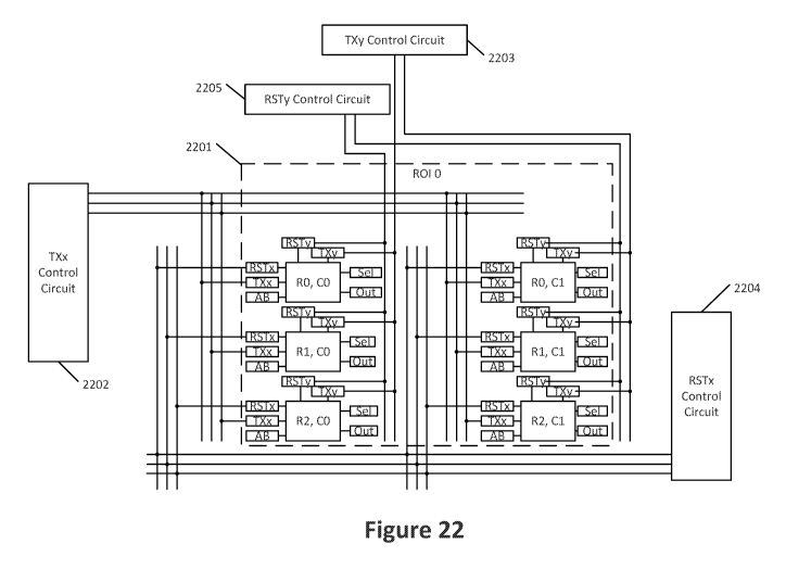
[0045] Figure 22 shows a circuit diagram with six pixels in an ROI.
8
SUBSTITUTE SHEET (RULE 26)
CA 03164318 2022-06-10
WO 2021/118971 PCT/US2020/063739
[0046] Figure 23 shows a block diagram of control circuitry and a CMOS
array with ROls
managed by different control circuitry.
[0047] Figure 24 shows a block diagram of control circuitry and a CMOS
array with
responsibility for ROls shared among different control circuitry.
[0048] Figure 25 shows a circuit diagram with six pixels in an ROI
controlled by different sets
of control circuitry.
[0049] Figure 26 shows a pixel with multiple transfer select signals,
multiple reset select
signals, and multiple output selection transistors.
[0050] Figure 27 shows a process for scheduling when ROls are to be
activated.
[00511 Figure 28 shows a block diagram of a hardware computing device.
[0052] It will be recognized by the skilled person in the art, given the
benefit of this disclosure,
that the exact arrangement, sizes and positioning of the components in the
figures is not
necessarily to scale or required. The particular sizes and angles of one
component
relative to another component may vary to provide a desired response or output
from
the component or the optical spectrometer system. comprising the component.
DETAILED DESCRIPTION
[0053] The accompanying drawings, which form a part hereof, show examples
of the
disclosure. It is to be understood that the examples shown in the drawings
and/or
discussed herein are non-exclusive and that there are other examples of how
the
disclosure may be practiced
[0054] Optical sensors are used in various applications and across
industries. Charge coupled
devices (CCDs) have been used since the 1970s. Recently, CMOS sensors have
become
more prevalent based on CMOS sensors being faster and generally less expensive
than
CCD sensors.
[0055] A random access CMOS sensor may be used in a variety of environments
including
those environments in which high speed sensing of regions of interest (ROI) is
required.
For example, a random access CMOS sensor may be used in diagnostic or testing
equipment including, but not limited to, spectrometers, high-speed cameras,
and remote
sensors. With respect to spectrometers, the random access CMOS sensor may be
used
to capture light at multiple wavelengths. Because the locations of the light
output from
a spectrometer may be known ahead of time (e.g., based on the configuration of
the
9
SUBSTITUTE SHEET (RULE 26)
CA 03164318 2022-06-10
WO 2021/118971 PCT/US2020/063739
spectrometer), the ROIs may be limited to those specific areas where the light
is
expected to be received across the pixel array.
[0056] CMOS pixels, like other light sensing devices, may be used as light
intensity measuring
devices when the pixels are properly exposed. Overexposing or underexposing a
pixel
may prevent light from being accurately measured by the pixel. A random access
CMOS
pixel, using the techniques shown in the figures and described in the
accompanying text,
permits one or more of variable exposure times and/or use of different ROIs in
a high-
speed environment. For purposes of explanation, the term "pixel" is used to
describe
picture elements in a sensor array in which each pixel includes a photodiode
or other
photosensitive device. The term "circuit" is used to describe a combination of
components. For example, the term "circuit" may be used to describe an
addressable
collection of devices in a sensor array, in which the collection of devices
may or may
not include a photodiode or other photosensitive device,
[0057] Figure 1 includes a photodiode "101 connected between a potential
(e.g., ground) and an
output transistor in a source-follower configuration. The gate of the output
transistor
108 (in this disclosure, it can be understood that all references to an
"output transistor"
may refer to a transistor in a source-follower configuration) connects to a
terminal of
the photodiode 101 and to a drain of a reset transistor 105, where the reset
transistor 105
is controlled by a reset signal 106 connected to its gate. The source of the
reset transistor
105 is connected to a potential shown as VRsT 102. In Figure 1, a floating
diffusion node
104 is located at the gate of output transistor 108. A selection transistor
109 connects a
terminal (source/drain) of output transistor 108 to one or more output lines
(one or more
output nodes) leading to a reading circuit (not shown). It shall be understood
herein that
a reading circuit corresponds to a single analog-to-digital converter ("ADC")
channel.
The selection transistor 109 may be controlled by a select signal 110
connected to the
gate of the selection transistor 109. In Figure 1 and the remaining figures of
the
disclosure, the transistors may be of similar or disparate types (including p-
type, n-type,
or combination thereof). For purposes herein, the term "gate" when used with
respect to
a terminal of a transistor is intended to refer to the gate terminal of the
transistor. Also,
the term "output nodes" may be used to describe the output of selection
transistors (e.g.,
selection transistor 109 or other selection transistors described herein). It
can thus be
SUBSTITUTE SHEET (RULE 26)
CA 03164318 2022-06-10
WO 2021/118971 PCT/US2020/063739
understood that the select signal 110 can be a signal that is associated with
e.g., a row
selection in an array of pixels, while the reading circuit signal can be a
signal that can
be associated with e.g., a column of an array of pixels, or vice-versa.
[00581 The 0,40S pixel of Figure 1 may be described as having various
operational states
including: a reset state (B) in which charges on the output of the photodiode
101 and/or
floating diffusion node 104 are reset; an exposure state (Exp) during which
the
photodiode 101 is permitted to charge a terminal of the output transistor 108;
and a read-
out state (RO) during which the output transistor 108 transfers the potential
difference
between VDD 107 and the photodiode 101 to a terminal (e.g., source/drain) of
selection
transistor 109. The selection transistor 109 may be operated to permit the
reading circuit
to read the potential selectively supplied to selection transistor 109 by
output transistor
108 (based on the accumulated charges on the gate of output transistor 108).
[0059] The Figures of the disclosed methods and systems include the use of
one or more
potentials, and it can be understood that such potentials may be different;
however, in
some embodiments, they may be the same,
[0060] Figure 2 shows a circuit similar to that of Figure 1 but including
an additional transfer
transistor 202 positioned between a floating diffusion node 204 and a
photodiode 201,
which is in turn connected to a potential (e.g., ground). The transfer
transistor 202 may
be controlled by a transfer signal 203 connected to the gate of the transfer
transistor 202.
The transfer transistor 202 connects the photodiode 201 to a floating
diffusion node 204.
A reset transistor 205 may connect the floating diffusion node 204 with a
constant
potential, represented in Figure 2 as Vat) 207. The reset transistor 205 may
be controlled
by a reset signal 206 connected to the gate of the reset transistor 205. A
gate of an output
transistor 208 may be connected to the floating diffusion node 204 and a
terminal (e.g.,
source/drain) of the output transistor 208 may be connected to a terminal of a
selection
transistor 209. The other terminal of the output transistor 208 may be
connected to a
constant potential (here, VDD 207). The selection transistor 209 connects the
terminal of
the output transistor 208 to one or more output lines leading to a reading
circuit (not
shown). The selection transistor 209 may be controlled by a select signal 210
connected
to the gate of the selection transistor 209. The output transistor 208 (as
also shown in
Figure 1, 108) provides a high impedance to the floating diffusion node 204,
thereby
11
SUBSTITUTE SHEET (RULE 26)
CA 03164318 2022-06-10
WO 2021/118971 PCT/US2020/063739
permitting a more consistent read operation across an array of pixels. The
addition of
transfer transistor 202 permits inclusion of another reset state (e.g., reset
state (F) in
which the floating diffusion node 204 is reset (e.g., to remove dark current,
parasitic
sensitivity, etc.). Thus, four states may be identified with Figure 2: a reset
state (B)
(during which charges on the output of photodiode 201 and/or floating
diffusion node
204 are reset), an exposure state (Exp) (during which the photodiode 201 is
permitted.
to accumulate charge), a reset state (F) (during which the floating diffusion
node is
reset), and a read-out state (RO) (during which charge accumulated by the
photodiode
201 is transferred to the floating diffusion node).
[0061] -Figure 3 shows a pixel according to Figure 1, but with an anti-
blooming connection. An
anti-blooming transistor 310 may be connected between the photodiode 301 and a
constant voltage potential (here, VDD 307). An anti-bloomin.g signal 311 may
be
connected to the gate of the anti-bloomin.g transistor 310,
[0062] In some applications, the entire pixel array may be operated to
obtain an image
illuminating the array. In other applications, only specific regions of
interest (ROIs) may
be desired to be monitored. By reducing the number of pixels to be activated
during
operation of the CMOS sensor and the corresponding state control of each pixel
(e.g.,
reset, exposed, reset, and read out), the effective speed of the CMOS sensor
may be
increased. For example, in some applications, an entire row may be selected
for
exposure. The row may be exposed as part of a global shutter or a rolling
shutter. An
issue with e.g., exposing an entire row, is the inability to subsequently
expose other
pixels on the same row for a different period of time. Similar issues exist
when e.g.,
attempting to read pixels that share a common column, as attempting to read
two pixels
in the same column at the same time creates a "collision" between the reading
states of
the pixels (i.e., charges from the two pixels are fed to a common column at
the same
time, thereby preventing a reading circuit from distinguishing between the
charges of
the two pixels). A similar issue may exist for collisions occurring when
attempting to
read data from pixels in the same row.
[0063] As described in relation to Figure 4 and subsequent figures, the
disclosed systems and.
methods include a CMOS sensor array that allows for individualized pixel
control. As
shown in Figure 4, such systems, methods, and/or circuits may achieve this
through the
12
SUBSTITUTE SHEET (RULE 26)
CA 03164318 2022-06-10
WO 2021/118971 PCT/US2020/063739
use of a rolling shutter that exposes selected portions of the CMOS sensor
array at a
time where a transfer transistor and/or reset transistor may be controlled by
more than
one transfer select signal, or more than one reset select signal. As such,
rolling shutters
for individual pixels may have overlapping exposure times or non-overlapping
exposure
times. Depending on the control circuitry, readout intervals may be
concatenated or
permitted to overlap each other. For example, for a given ROI, similar
waveforms may
be used to control the various transfer, reset, and select transistors. Those
similar
waveforms may or may not be shifted in time from each other.
[0064] Figure 4 shows a pixel with a gate of a transfer transistor
controlled by two transfer
select signals, TXx 411 and TXy 412. Figure 4 includes a photodiode 401
connected
between a potential (e.g., ground) and a transfer transistor 402. The transfer
transistor
402 may be controlled by a transfer signal connected to the gate of the
transfer transistor
402. As shown, two or more transfer select signals (TXx 411 and TXy 412)
driving the
gate of the transfer transistor 402 are thus used in combination to control
the transfer
transistor 402 and hence the functionality of the pixel, independent of the
other pixels,
including those that may be in the same row and/or column. As shown in Figure
4,
functionally, the two or more transfer select signals, TXx 411 and TXy 412,
can be
understood to be inputs to the equivalent of an AND logic gate 403, although
it can be
understood that this functionality can be achieved in many different ways, and
the
Figure 4 AND gate 403 is merely a representation of such functionality. The
transfer
transistor 402 connects the photodiode 401 to a floating diffusion node 404.
An optional
anti-blooming transistor 413 can connect the photodiode 401 to a potential
(e.g., VDD
407), and the gate of the anti-blooming transistor 413 can be driven by an
anti-blooming
select signal 414. A reset transistor 405 may connect the floating diffusion
node 404
with a constant potential, represented in Figure 4 as Von 407. The reset
transistor 405
may be controlled by a reset signal 406 connected to the gate of the reset
transistor 405.
A gate of an output transistor 408 may be connected to the floating diffusion
node 404
and a terminal (e.g., source/drain) of the output transistor 408 may be
connected to a
terminal of a selection transistor 409. The other terminal of the output
transistor 408
may be connected to a constant potential (here, VDD 407). The selection
transistor 409
connects a terminal of the output transistor 408 to one or more output lines
leading to a
13
SUBSTITUTE SHEET (RULE 26)
CA 03164318 2022-06-10
WO 2021/118971 PCT/US2020/063739
reading circuit (not shown). The selection transistor 409 may be controlled by
a select
signal 410 connected to the gate of the selection transistor 409.
[0065] Benefits of having multiple transfer select lines includes one or
more of the following:
individual control of pixels, allowing each pixel to be individually
addressed; increasing
the flexibility of when specific ROIs are enabled to be reset, exposed; reset,
and read
out; controlling collisions during these operations by permitting ordering of
the states
per ROI across a CMOS sensor; increasing the flexibility of ROIs on the CMOS
sensor
by permitting ROIs to have different sizes, locations, and exposure times;
increasing the
flexibility of the readout times per ROI, and increasing the flexibility of
the number of
states available per ROI.
[0066] Figure 5 shows one example timing diagram for a CMOS sensor according
to Figure 4.
Figure 5 includes reset signal 406, a first transfer select signal TXx 411,
and a second
transfer select signal TXy 412. Figure 5 also shows the operation of the reset
transistor
405 in response to the reset signal 406. When the reset signal 406 changes
from a first
level to a second level. (shown in Figure 5 as transitioning from a low-
voltage state to a
high-voltage state), the reset transistor is turned on,
[0067] Figure 5 further shows the operation of transfer transistor 402 in
response to the
combination of the first and second transfer select signals TXx 411 and TXy
412. When
both the first and second transfer select signals TXx 411 and TXy 412 are in
the high-
voltage state, the transfer transistor turns on. However, when one or both of
the transfer
select signals TXx 411 and TXy 412 are in the low-voltage state, the transfer
transistor
is of
[0068] The transistors shown in the figures and described in the
specification may be edge-
triggered, level-triggered or combination of bath. Accordingly, for example,
with
respect to Figure 5, the reset transistor and/or the transfer transistor may
only turn on
with the respective triggering method.
[0069] Figure 6 shows an example of a logic table of the operation of the
transfer transistor of
Figure 4 using the two transfer select signals. Two possible values {0,1} for
the first
TXx transfer select signal are shown as row identifiers in the table of Figure
6 and two
possible values 10,11 for the second TXy transfer select signal are shown as
column
identifiers in the table of Figure 6. When at least one of the transfer select
signals is {0},
14
SUBSTITUTE SHEET (RULE 26)
CA 03164318 2022-06-10
WO 2021/118971 PCT/US2020/063739
the transfer transistor is off. When both of the transfer select signals is
{1}, the transfer
transistor is on.
[0070] Figure 7 shows a circuit that can be, e.g., a pixel of a CMOS
sensor, with a gate of a
transfer transistor 702 controlled by two transfer select signals and a gate
of a reset
transistor 705 controlled by two reset select signals, thereby allowing for
individualized
transfer and reset of the pixel relative to other pixels in the array. Figure
7 includes a
photodiode 701 connected between a potential (e.g., ground) and a transfer
transistor
702. Optionally, the photodiode 701 can be additionally connected to an anti-
blooming
transistor 715 that can be driven by an anti-blooming select signal 716. The
transfer
transistor 702 may be controlled by a transfer signal (represented
functionally in Figure
7 as an ANT) logic gate 703) connected to the gate of the transfer transistor
702. The
transfer transistor 702 connects the photodiode 701 to a floating diffusion
node 704. A
reset transistor 705 may connect the floating diffusion node 704 with a
constant
potential, represented in Figure 7 as VDD 707. The reset transistor 705 may be
controlled
by a reset signal (represented functionally in Figure 7 as an AND logic gate
706)
connected to the gate of the reset transistor 705. A. gate of an output
transistor 708 may
be connected to the floating diffusion node 701 and a terminal (e.g.,
source/drain) of the
output transistor 708 may be connected to a terminal of a selection transistor
709. The
other terminal of the output transistor 708 may be connected to a constant
potential
(here. VDD 707). The selection transistor 709 connects the terminal of the
output
transistor 708 to one or more output lines leading to a reading circuit (not
shown). The
selection transistor 709 may be controlled by a select signal 710 connected to
the gate
of the selection transistor 709. The AND logic gate 703 may receive as inputs
two or
more transfer select signals, represented by first and second transfer select
signals TXx
711 and TXy 712. By using two or more transfer select signals for a given
transfer
transistor, the transfer transistor may be individually addressed as compared
to
addressing solely an entire row (or column) of transfer transistors. The
Figure 7 reset
select AND logic gate 706 may receive as inputs two or more reset select
signals,
represented by first and second reset select signals RSTx 713 and RSTy 714. By
using
two or more reset select signals for a given reset transistor, the reset
transistor may be
individually addressed as compared to addressing solely an entire row (or
column) of
SUBSTITUTE SHEET (RULE 26)
CA 03164318 2022-06-10
WO 2021/118971 PCT/US2020/063739
reset transistors.
[0071] Figure 8 shows one example timing diagram in accordance with a
circuit, e.g., pixel of
a CMOS sensor, according to Figure 7, with two transfer select signals and two
reset
select signals. With reference to the Figure 7 circuit, Figure 8 includes a
first reset select
signal RSTx 713, a second reset select signal RSTy 714 being a different width
(or in a
"high" state for a different (e.g., longer or shorter) period of time) than
the first reset
signal RSTx 713, a first transfer select signal TXx 711, and a second transfer
select
signal TXy 712 being a different width (or in a "high" state for a different
period of
time) as the first transfer select signal TXx 711, although it can be
understood that the
first and second reset select signals RSTx and RSTy, as well as the first and
second
transfer select signals TXx and TXy, may be the same width/duration (or "high"
for the
same amount of time), or a different (e.g., relatively "longer" or "shorter")
widthlduration. (e.g., the RST transistors relative to the TX transistors or
the RSTx/TXx
transistors relative to the RSTy./TXy transistors). Accordingly, as with the
various
example timing diagrams provided herein, it may be found that other variations
of the
timing diagrams may be more suitable to a particular application, and the
present
disclosure shall not be limited by such timing diagram examples.
[0072] Figure 8 shows the operation of the reset transistor 705 in response
to the shown first
and second reset signals RSTx 713 and RSTy 714. As illustrated, when both the
reset
select signals RSTx 713 and RSTy 714 are in the high-voltage state, the reset
transistor
is on. However, when one or both of the reset select signals RSTx 713 and RSTy
714
are in the low-voltage state, the reset transistor is off. In some embodiments
such as the
example embodiment of Figure 7 and 8, it may be determined that TXx is higher
for a
longer period of time than TXy, and similarly, RSTx is higher for a longer
period of
time than RSTy.
[0073] Figure 8 further shows the operation of transfer transistor '702 in
response to the
combination of transfer select signals TXx 711 and TXy 712. When both the
transfer
select signals TXx 711 and TXy 712 are in the high-voltage state, the transfer
transistor
is on. However, when one or both of the transfer select signals 'Da 711 and
TXy 712
are in the low-voltage state, the transfer transistor is off
[0074] Figure 9A shows an example logic table for the operation of the
reset transistor in
16
SUBSTITUTE SHEET (RULE 26)
CA 03164318 2022-06-10
WO 2021/118971 PCT/US2020/063739
response to the first and second reset select signals 713, 714. Two values
{0,1) for the
RSTx reset select signal are shown as row identifiers in the table of Figure
9A and two
values {0,1} for the RSTy reset select signal are shown as column identifiers
in the table
of Figure 9A. When at least one of the reset select signals is (0), the reset
transistor is
off. When both of the reset select signals is 11 ) the reset transistor is on.
[0075] Figure 9B shows an example logic table for the operation of the
transfer transistor in
response to the transfer select signals. Two values {0,11 for the TXx transfer
select
signal are shown as row identifiers in the table of Figure '_:.)13 and two
values 10,1} for
the TXy transfer select signal are shown as column identifiers in the table of
Figure 9B.
When at least one of the transfer select signals is {0}, the transfer
transistor is off. When
both of the transfer select signals is (1 , the transfer transistor is on.
[0076] Figure 10A shows a circuit, e.g., a pixel of a CMOS sensor, in
accordance with the
circuit of Figure 7, however, with the functionality of the ANT) gates
replaced with
transistors. In the Figure 10A embodiment, separate transistors control the
operation of
a transfer transistor 1002 and a reset transistor 1005. A.s will be described
herein, in the
Figure 10A embodiment, the transfer transistor 1002 and reset transistor 1005
are
"floating," Figure 1.0A includes a photodiode 1001 connected between a
potential (e.g.,
VSS) and the transfer transistor 1002. The transfer transistor 1002 is
connected between
the photodiode 1001 and a -floating diffusion node 1004. The gate of the
transfer
transistor 1002 is connected to the output of a transfer selection transistor
1003. A gate
of the transfer selection transistor 1003 receives a first transfer select
signal TX*. The
transfer selection transistor 1003 is connected between the gate of transfer
transistor
1002 and a second transfer select signal TXy. Similarly, the reset transistor
1005 is
connected between the 'floating diffusion node 1004 and a potential (e.g.,
'VDDrst). A
gate of a reset selection transistor 1006 receives a first reset select signal
RSTx. The
reset selection transistor 1006 is connected between a gate of the reset
transistor 1005
and a second reset select signal RSTy. An output transistor 1008 is connected
between
a potential (e.g., 'VDDpix) and a selection transistor 1009. The gate of the
output
transistor 1008 is connected to the floating diffusion node 1004. The
selection transistor
1009 is connected between the output transistor 1008 and reading circuitry
(not shown).
The gate of the selection transistor 1009 receives a select signal SEL. An
optional anti-
17
SUBSTITUTE SHEET (RULE 26)
CA 03164318 2022-06-10
WO 2021/118971 PCT/US2020/063739
blooming transistor 1016 is connected between the photodiode 1001 and a
potential
(e.g., VDDpix). A gate of the anti-blooming transistor 1016 receives an anti-
blooming
select signal AB.
[00771 Figure 10B shows an alternative view of the pixel of Figure 10A with
additional
annotations. Figure 10B includes a photodiode 1001 connected between a
potential
(e.g., ground) and a transfer transistor 1002. The transfer transistor 1002
may be
controlled by the output of a transfer selection transistor 1003 connected to
the gate of
the transfer transistor 1002. The transfer transistor 1002 connects the
photodiode 1001
to a floating diffusion node 1004. A reset transistor 1005 may connect the
floating
diffusion node 1004 with a constant potential, represented in Figure 10B as -
VDDrst
1007. The reset transistor 1005 may be controlled by a reset selection
transistor 1006
connected to the gate of the reset transistor 1005. A gate of an output
transistor 1008
may be connected to the floating diffusion node 1004 and a terminal (e.g.,
source/drain)
of the output transistor 1008 may be connected to a terminal of a selection
transistor
1009. The other terminal of the output transistor 1008 may be connected to a
constant
potential (here, VDDsf 1015). The constant potentials VDDrst 1007 and VDDsf
1015
may be the same or different. The selection transistor 1009 connects the
terminal of the
Output transistor 1008 to one or more output lines leading to a reading
circuit (not
shown). The selection transistor 1009 may he controlled by a select signal
1010
connected to the gate of the selection transistor 1009. The transfer selection
transistor
1003 may receive as inputs two or more transfer select signals, represented by
transfer
select signals TXx 1011 and TXy 1012. For example, a gate of the transfer
selection
transistor 1003 may receive the transfer select signal TXx 1.011 and have its
remaining
terminal (e.g., the other of the source/drain not connected to the gate of the
transfer
transistor 1002) connected to the transfer select signal TXy 1012. By using
two or more
transfer select signals for a given transfer selection transistor 1003, the
transfer transistor
1002 may be individually addressed as compared to addressing solely an entire
row of
transfer transistors. The reset selection transistor 1006 may receive as
inputs two or
more reset select sianals, represented by reset select signals RSTx 1013 and
RSTy 1014.
For example, a gate of the reset selection transistor 1006 may receive the
reset select
signal RSTx 1013 and have its remaining terminal (e.g., the other of the
source/drain
18
SUBSTITUTE SHEET (RULE 26)
CA 03164318 2022-06-10
WO 2021/118971 PCT/US2020/063739
not connected to the gate of the reset transistor 1005) connected to the reset
select signal
RSTy 1014. By using two or more reset select signals for a given reset
transistor, the
reset transistor 1005 may be individually addressed as compared to addressing
solely an
entire row of reset transistors. Figure 10B also includes an optional anti-
blooming
transistor 1016 connected to the photodiode 1001. The other end of anti-
blooming
transistor 1016 may be connected to a constant potential (e.g., VIMsf 1015). A
gate of
the anti-blooming transistor 1016 may receive an anti-blooming signal AB 1017.
[0078] Figure 11 shows an example timing diagram in accordance with the
Figure 10 circuit,
e.g., CMOS sensor, with first and second transfer select signals 1011, 1012
and first and
second reset select signals 1013, 1014. Figure 11 includes a reset select
signal RSTx
1013, a reset select signal RSTy 1014, a transfer select signal 1Xx 1011, and
transfer
select signal TXy 1012. Figure 11 shows the operation of the reset transistor
1005 in
response to the reset signal (the output of the reset selection transistor
1006). When both
the reset select signals RSTx 1013 and RSTy 1014 are in a high-voltage state,
the reset
transistor is on. However, when one or both of the reset select signals RSTx
1013 and
RSTy 1014 are in a low-voltage state, the reset transistor is off.
[0079] Figure 11 further shows the operation of transfer transistor 1002 in
response to the
combination of transfer select signals TXx 1011 and TXy 1012. When both the
transfer
select signals TXx 1011 and TXy 1012 are in a high-voltage state, the transfer
transistor
is on. However, when one or both of the transfer select signals TXx 1011 and
TXy 1012
are in a low-voltage state, the transfer transistor is off.
[0080] For circuits, e.g., pixels, according to Figures 10A and 10B, it can
be understood that
the example RSTx is shown with the same width (e.g., in a high state for the
same
amount of time) as TXx, and RSTy is shown with the same width as TXy, although
such
an embodiment is only illustrative, and other relationships between the
various TX and
RST signals may be used as determined by the use of the circuit. Additionally,
for the
example embodiment, as shown in Figure 11, RSTx, connected to the gate of the
reset
selection transistor 1006, may be longer (e.g., in a high state for a longer
period of time)
than the signal RSTy connected to the source of the reset selection transistor
1006,
although such example embodiment is only illustrative. Similarly, as also
shown in
Figure 11, TXx, connected to the gate of the transfer selection transistor
1003, may be
19
SUBSTITUTE SHEET (RULE 26)
CA 03164318 2022-06-10
WO 2021/118971 PCT/US2020/063739
longer (e.g., in a high state for a longer period of time) than the signal TXy
connected
to the source of the transfer selection transistor 1003.
[0081] Figure 12A shows an example logic table for the operation of the
reset selection
transistor, and hence reset transistor, using the first and second reset
select signals. Two
values {0,11 for the RSTx reset select signal are shown e.g., as row
identifiers in the
table of Figure 12A and two values {0,11 for the RS'Ty reset select signal are
shown
e.g., as column identifiers in the table of Figure 12A. When the RSTx signal
is {0}, the
reset selection transistor is floating. When the RSTx signal is {1} and the
RSTy signal
is {0}, the reset selection transistor is off (represented by a {0}). When
both of the reset
select signals is {1}, the reset selection transistor, and hence the reset
transistor, is on
(represented by a {1}).
[0082] Figure 1_2B shows an example logic table for the operation of the
transfer selection
transistor using first and second transfer select signals. Figure 12B shows an
example
of a logic table of the operation of the transfer selection transistor of
Figure 10B using
the first and second transfer select signals. Two values {OM for the TXx
transfer select
signal are shown as e.g., row identifiers in the table of Figure 12B and two
values {0,1}
for the TXy transfer select signal are shown as e.g., column identifiers in
the table of
Figure 12B, When the TXx signal is {01, the transfer selection transistor is
floating.
When the TXx signal is {1} and the TXy signal is {0}, the transfer selection
transistor
is off (represented by a {0}). When bath of the transfer select signals are
{1} , the transfer
selection transistor, and hence the transfer transistor, is on (represented by
a (1)).
[0083] Figure 13A shows an embodiment of a circuit, e.g., a pixel of a CMOS
sensor, similar
to Figure 10A, except that the transfer and reset transistors are not
floating, but biased.
As shown in Figure 13A, there is a transfer transistor 1302 controlled by two
transfer
selection transistors 1303a, 1303b and a reset transistor 1305 controlled by
two reset
selection transistors 1306a, 1306b. Figure 13A includes a photodiode 1301
connected
between a potential (e.g., VSS) and the transfer transistor 1302. The transfer
transistor
1302 is connected between the photodiode 1301 and the 'floating diffusion node
1304.
The gate of the transfer transistor 1302 is connected to the output of a first
transfer
selection transistor 1303a. A gate of the first transfer selection transistor
1303a receives
a first transfer select signal T.Xx. The first transfer selection transistor
1303a is
SUBSTITUTE SHEET (RULE 26)
CA 03164318 2022-06-10
WO 2021/118971 PCT/US2020/063739
connected between the gate of transfer transistor 1302 and a second transfer
select signal
TXy. A second transfer selection transistor 1303b is connected between the
gate of the
transfer transistor 1302 and a potential (e.g., VSS). The second transfer
selection
transistor 1303b is connected to a complement of the first transfer select
signal (e.g.,
TXx_n). Also shown is a reset transistor 1305 connected between the floating
diffusion
node 1304 and a potential (e.g., VDDrst). A gate of a first reset selection
transistor
1306a receives a first reset select signal RSTx. The first reset selection
transistor 1306a
is connected between a gate of the reset transistor 1305 and a second reset
select signal
RSTy. A second reset selection transistor 1306b is connected between the gate
of the
reset transistor 1305 and a potential (e.g., VSS). The second reset selection
transistor
1306b is connected to a complement of the first reset select signal (e.g.,
R.STx_n.), An
output transistor 1308 is connected between a potential (e.g., VDDpix) and a
selection
transistor 1309. The gate of the output transistor 1308 is connected to the
floating
diffusion node 1304. The selection transistor 1309 is connected between the
output
transistor 1308 and reading circuitry (not shown.), The gate of the selection
transistor
1309 receives a select signal SIT. An optional anti-blooming transistor 1316
is
connected between the photodiode 1301 and a potential (e.g., NiT)Dpix.). .A
gate of the
anti-blooming transistor 1316 receives an anti-blooming select signal AB.
[0084] Figure 13B shows an alternative view of the circuit (e.g., pixel) of
Figure 13A with
additional annotations. Figure 13B includes a photodiode 1301 connected
between a
potential (e.g., ground) and a transfer transistor 1302, The transfer
transistor 1302 may
be controlled by the output of a transfer selection transistor I 303a
connected to the gate
of the transfer transistor 1302. The transfer transistor 1302 connects the
photodiode
1301 to a floating diffusion node 1304. A reset transistor 1305 may connect
the floating
diffusion node 1304 with a constant potential, represented in Figure 13B as
VDDrst
1307. The reset transistor 1305 may be controlled by a reset selection
transistor 1306a
connected to the gate of the reset transistor 1305. A gate of an output
transistor 1308
may be connected to the floating diffusion node 1304 and a terminal (e.g.,
source/drain)
of the output transistor 1308 may be connected to a terminal of a selection
transistor
1309. The other terminal of the output transistor 1308 may be connected to a
constant
potential (here, VDDsf 1315). The constant potentials VDDrst 1307 and VDDsf
1315
21
SUBSTITUTE SHEET (RULE 26)
CA 03164318 2022-06-10
WO 2021/118971 PCT/US2020/063739
may be the same or different. The selection transistor 1309 connects the
terminal of the
output transistor 1308 to one Or more output tines leading to a reading
circuit (not
shown). The selection transistor 1309 may be controlled by a select signal
1310
connected to the gate of the selection transistor 1309. The transfer selection
transistor
1303a may receive as inputs two or more transfer select signals, represented
by transfer
select signals TXx 1311a and TXy 1312. For example, a gate of the transfer
selection
transistor 1303a may be connected to the transfer select signal TXx 1311a. and
have its
remaining terminal (e.g., the other of the source/drain not connected to the
gate of the
transfer transistor 1302) connected to the transfer select signal TXy 1312.
Figure 13B
includes another transfer selection transistor 1303b connected between the
gate of
transfer transistor 1302 and a constant potential (e.g., ground). The gate of
the transfer
selection transistor 1303b may be connected to a complement of transfer select
signal
TXx 1311.a (namely, a transfer select signal /TXx 131 lb). By using two or
more transfer
select signals for a given transfer transistor, the transfer transistor may be
individually
addressed as compared to addressing solely an entire row (or column) of
transfer
transistors.
[0085] The transfer selection transistors 1303a and 1303b may be the same
type of transistor
(p-type or n-type). Additionally or alternatively, the transfer selection
transistors 1303a
and 1303b may be different types of transistors (one p-type and one n-type).
By the
transfer selection transistors 1303a and 1303b being different types of
transistors, the
sam.e transfer select signal TXx 1311a may be applied to the gates of the two
transfer
selection transistors. With a high gate voltage, one turns on and the other
turns off.
Similarly, with a low gate voltage, one turns off and the other turns on. This
approach
reduces adding a separate inverter to create the complementary /TXx 1311b
signal.
[00861 The reset selection transistor 1306a may be connected to two or more
reset select
signals, represented by reset select signals RSTx 1313a and RSTy 1314. For
example,
a gate of the reset selection transistor 1306a may be connected to the reset
select signal
RSTx 1313a and have its remaining terminal (e.g., the other of the
source/drain not
connected to the gate of the reset transistor 1305) connected to the reset
select signal
RSTy 1314. Figure 13B includes another reset selection transistor 1306b
connected
between the gate of reset transistor 1305 and a constant potential (e.g.,
ground). The
22
SUBSTITUTE SHEET (RULE 26)
CA 03164318 2022-06-10
WO 2021/118971 PC T/US2020/063739
gate of the reset selection transistor 1306b may be connected to a complement
of reset
select signal RSTx 1313a (namely, a reset select signal /RSTx 1313b). By using
two or
more reset select signals for a given reset transistor, the reset transistor
may be
individually addressed as compared to addressing solely an entire row (or
column) of
reset transistors.
[0087] The reset selection transistors 1306a and 1306b may be the same type
of transistor (p-
type or n-type). Additionally or alternatively, the reset selection
transistors 1306a and
1306b may be different types of transistors (one p-type and one n-type). By
the reset
selection transistors 1306a and 1306b being different types of transistors,
the same reset
select signal RSTx 1313a may be applied to the gates of the two reset
selection
transistors. With a high gate voltage, one turns on and the other turns off,
Similarly,
with a low gate voltage, one turns off and the other turns on. This approach
reduces
adding a separate inverter to create the complementary /RSTx 1313b signal.
[0088] Figure 13B also includes an optional anti-blooming transistor 1316
connected to
photodiode 1301. The other end of anti-blooming transistor 1316 may be
connected to
a constant potential (e.g., NIDDsf 1315). .A gate of the anti-blooming
transistor 1316
may receive an anti-blooming signal AB 1317.
[0089] Figure 14 shows one timing diagram of a circuit. e.g., CMOS sensor,
with two transfer
select signals and two reset select signals according to Figure 13B. Figure 14
includes
a reset select signal represented by RSTx and its complement /RSTx, a reset
select signal
RSTy, a transfer select signal represented by TXx and its complement /TXx, and
transfer select signal TXy. Figure 14 shows the operation of the reset
transistor 1305 in
response to the reset signal (the output of the reset selection transistor
1306a and the
reset selection transistor 1306b). When the reset select signals RSTx 1313a
and RSTy
1314 are in the high-voltage state and the reset select signal /RSTx 1313b is
in the low-
voltage state, the reset transistor is on. However, when reset select signal
RSTx is in the
low-voltage state and the reset select signal /RSTx is in the high-voltage
state, the reset
transistor 1305 is off. Similarly, when the reset select signal RSTy is in the
low-voltage
state, the reset transistor 1.305 is off.
[0090] Figure 14 further shows the operation of transfer transistor 1302 in
response to the
transfer signal (the output of the transfer selection transistor 1303a and the
transfer
23
SUBSTITUTE SHEET (RULE 26)
CA 03164318 2022-06-10
WO 2021/118971 PCT/US2020/063739
selection transistor 1303b). When the transfer select signals TXx 1311a and
TXy 1312
are in the high-voltage state and the transfer select signal /DCx 1311b is in
the low-
voltage state, the transfer transistor is on. However, when transfer select
signal TXx is
in the low-voltage state and the transfer select signal frXx is in the high-
voltage state,
the transfer transistor 1302 is off. Similarly, when the transfer select
signal TXy is in
the low-voltage state, the transfer transistor is off. It can be understood
that although
Figure 14 shows transfer select signals TXx and 'DCA/ having the same
length/duration
in a high-voltage/potential state, such equivalence of duration is not
required and may
be different between the two signals.
[0091] Figure 15A shows an example logic table for the operation of the
reset transistor using
the reset select signals, For purposes of explanation, a full logic table is
shown for the
reset select signals RSTx 1313a, /RSTx 1313b, and RSTy 1.314, each having
values
{0,1}. When the RSTx signal is {0} and the IRSTx signal is Ill, the reset
transistor is
off (represented by {0}). When the RSTx signal is {11, the /RSTx signal is
{0}, and the
RSTy signal is {0}, the reset transistor is off (represented by a (01). When
the RSTx
and RSTy signals are {1} and the /RSTx signal is {0}, the reset transistor is
on
(represented by a {1}). Rows in which RSTx and ,'RSTx have the same value
include
single asterisks "*" following the values of each to identify that the signals
being
supplied to the gates of reset selection transistors 1306a and 1306b are not
always
complementary (namely, they may be the same, e.g., when derived from different
sources). In these rows, the reset transistor is identified as floating.
Further, in rows with
double asterisks "**", the reset selection transistors 1306a and 1306b are
bath on and
may result in a high current draw.
[0092] Figure 15B shows an example logic table for the operation of the
transfer transistor
using the transfer select signals. For purposes of explanation, a full logic
table is shown
for the transfer select signals TXx 1311a, /TXx 1311b, and TXy 1312, each
having
values [0,11. When the TXx signal is 101 and the frXx signal is 111, the
transfer
transistor is off (represented by (01). When the TXx signal is {1}, the frXx
signal is
{0}, and the TXy signal is {O}, the transfer transistor is off (represented by
a {0}). When
the TXx and TXy signals are {1} and the IOU signal is {0}, the transfer
transistor is
on (represented by a {1}). Rows in which TXx and /TXx have the same value
include
24
SUBSTITUTE SHEET (RULE 26)
CA 03164318 2022-06-10
WO 2021/118971 PCT/US2020/063739
single asterisks "*" following the values of each to identify that the signals
being
supplied to the gates of transfer selection transistors 1303a and 1303b are
not always
complementary (namely, they may be the same, e.g., when derived from different
sources). In these rows, the transfer transistor is identified as floating.
Further, in rows
with double asterisks "**", the transfer selection transistors 1303a and 1303b
are both
on and may result in a high current draw.
[0093] Figure 16A shows another embodiment of a circuit, e.g., a pixel,
similar to that shown
in Figure 13A, except the transfer transistor is shown by a first transfer
circuit 1602
whose functionality is shown for explanatory purposes with two transfer
transistors
1603a, 1603b. It can be understood that in embodiments, the transfer circuit
1602 can
be implemented using a single transistor with two gate pins. Figure 16A
includes a
photodiode 1601 connected between a potential (e.g., VSS) and transfer circuit
1602.
The transfer circuit 1602 is connected between the photodiode 1601 and a
floating
diffusion node 1604. The transfer circuit 1602 may be one or more transfer
transistors,
each controlled by a transfer select signal. For example, the transfer circuit
1602 (shown
in Figure 16A as an area defined by a dashed line) may include a series
connection of a
first transfer circuit selection transistor 1603a and a second transfer
circuit selection
transistor 1603b. The first transfer circuit selection transistor 1603a may
receive, at its
gate, a transfer select signal TXx. The second transfer circuit selection
transistor 1603b
may receive, at its gate, a transfer select signal TXY. A reset transistor
1605 is connected
between the floating diffusion node 1604 and a potential (e.g., VDDrst). A
gate of a
reset selection transistor 1606 receives a first reset select signal RSTx. The
reset
selection transistor 1606 is connected between a gate of the reset transistor
1605 and a
second reset select signal RSTy. An output transistor 1608 is connected
between a
potential (e.g., VDDpix) and a selection transistor 1609. The gate of the
output transistor
1608 is connected to the floating diffusion node 1604. The selection
transistor 1609 is
connected between the output transistor 1608 and reading circuitry (not
shown). The
gate of the selection transistor 1609 receives a select signal SEL. An
optional anti-
blooming transistor 1616 is connected between the photodiode 1601 and a
potential
(e.g., VDDpix). A gate of the anti-blooming transistor 1616 receives an anti-
blooming
select signal AB.
SUBSTITUTE SHEET (RULE 26)
CA 03164318 2022-06-10
WO 2021/118971 PCT/US2020/063739
[0094] Figure 16B is an alternative view of the circuit, e.g., pixel of
Figure 16A with additional
annotations. Figure 16B includes a photodiode 1601 connected between a
potential
(e.g., ground) and a transfer circuit 1602. The transfer circuit 1602.
connects the
photodiode 1601 to a floating diffusion node 1604. A reset transistor 1605 may
connect
the floating diffusion node 1604 with a constant potential, represented in
Figure 16B as
-VDDrst 1607. The reset transistor 1605 may be controlled by a reset selection
transistor
1606 connected to the gate of the reset transistor 1605. A gate of an output
transistor
1608 may be connected to the floating diffusion node 1604 and a terminal
(e.g.,
source/drain) of the output transistor 1608 may be connected to a terminal of
a selection
transistor 1609. The other terminal of the output transistor 1608 may be
connected to a
constant potential (here, NIDDsf 1615). The constant potentials VDDrst 1607
and
NIDDsf 1615 may be the same or different. The selection transistor 1609
connects the
terminal of the output transistor 1608 to one or more output lines leading to
a reading
circuit (not shown). The selection transistor 1609 may be controlled by a
select signal
1610 connected to the gate of the selection transistor 1609.
[0095] The second transfer circuit selection transistor 1603b may receive,
at its gate, a transfer
select signal TXx 1611, and as described previously, the first transfer
circuit selection
transistor 1603a may receive, at its gate, a transfer select signal TXy 1612.
By using
two or more transfer select signals for a given transfer transistor, the
transfer transistor
may be individually addressed as compared to addressing solely an entire row
(or
column) of transfer transistors.
[0096] The reset selection transistor 1606 may receive as inputs two or
more reset select
signals, represented by reset select signals RSTx 1613 and RSTy 1614. For
example, a
gate of the reset selection transistor 1606 may receive the reset select
signal RSTx 1613
and have its remaining terminal (e.g., the other of the source/drain not
connected to the
gate of the reset transistor 1605) connected to the reset select signal RSTy
1614.
Alternatively, the reset transistor 1605 may be a reset circuit comprising two
reset
transistors in a configuration similar to the transfer circuit 1602. By using
two or more
reset select signals for a given reset transistor, the reset transistor may be
individually
addressed as compared to addressing solely- an entire row (or column) of reset
transistors.
26
SUBSTITUTE SHEET (RULE 26)
CA 03164318 2022-06-10
WO 2021/118971 PCT/US2020/063739
[0097] Figure 16B also includes an optional anti-blooming transistor 1616
connected to
photodiode 1601. The other end of anti-blooming transistor 1616 may be
connected to
a constant potential (e.g., VDDsf 1615). A gate of the anti-blooming
transistor 1616
may receive an anti-blooming signal AB 1617.
[0098] Additionally or alternatively, the reset transistor 1605 may be a
reset circuit (similar to
that of transfer circuit 1602) in which a dual gate reset selection transistor
may be
connected in series between floating diffusion node 1604 and the potential
VDDrst
1607, in which one of the reset selection transistor gates is controlled by
RSTx 1613
and the other controlled by RSTy 1614.
[0099] Figure 17 shows an example timing diagram for a circuit, e.g., a
CMOS sensor, with
two transfer select signals and two reset select signals according to Figure
16B. Figure
17 includes a reset select signal RSTx, a reset select signal RSTy, a transfer
select signal
TXx, and transfer select signal TXy. Figure 17 shows the operation of a reset
transistor
in response to a reset signal, which is a combination of the reset select
signal RSTx and
the reset select signal RSTy. When both the reset select signals RSTx and RSTy
are in
the high-voltage state, the reset transistor is on. However, when one or both
of the reset
select signals RSTx and RSTy are in the low-voltage state, the reset
transistor is off.
[0100] Figure 17 further shows the operation of the transfer transistor in
response to the
combination of transfer select signals TXx and TXy. When bath the transfer
select
signals TXx and TXy are in the high-voltage state, the transfer transistor is
on. However,
when one or both of the transfer select signals DU. and TXy are in the low-
voltage state,
the transfer transistor is off.
[0101] Figure 18A shows an example logic table for the operation of the
reset transistor using
two reset select signals as shown in Figure 16B. Two values {0,1} for the RSTx
reset
select signal are shown as row identifiers in the table of Figure 18A and two
values
{0,1} for the RSTy reset select signal are shown as column identifiers in the
table of
Figure 18A. When the RSTx signal is {0), the reset transistor is floating.
When the
RSTx signal is {1} and the RSTy signal is f0}, the reset transistor is off
(represented by
a {0}). When both of the reset select signals is {1}, the reset transistor is
on (represented
by a {1}).
[0102] Figure 18B shows an example logic table for the operation of the
transfer transistor
27
SUBSTITUTE SHEET (RULE 26)
CA 03164318 2022-06-10
WO 2021/118971 PCT/US2020/063739
using two transfer select signals as shown in Figure 16B. Two values {0,i for
the
transfer select signal TXx are shown as row identifiers in the table of Figure
18B and
two values {0,1} for the transfer select signal TXy are shown as column
identifiers in
the table of Figure 18B. When the TXx signal is [01, the transfer transistor
is off
(represented by a {O}). When the TXx signal is {1} and the TXy signal is {O},
the reset
transistor is off. When both of the transfer select signals are {1}, the
transfer transistor
is on (represented by a Ill).
[01031 Figure 19 shows an exemplary timing diagram for reset and transfer
transistors with
multiple reset and transfer select signals. Figure 19 shows an ROI with four
pixels in
four rows and in a common column. ROI 1 includes pixels in each of row j, row
.1+1,
row J+2, and row J 3. The pixels are exposed using a rolling shutter. Figure
19 timing
diagram is for the reset select signals and the transfer select signals for
each of the four
pixels. The first pixel (in row J) enters the B reset state when the RSTx<J>,
T.Xx<J>,
RSTy<cols> and TXy<cols> signals are high. The second pixel (in row J+1)
enters the
B reset state when the RSTx<J+1>, T.Xx<J+1 , RSTy<cols> and TXy<cols> signals
are high. The third pixel (in row J+2) enters the B reset state when the
R.STx<J+2>,
TXx<J+2>, RSTy<cols> and TXy<cols> signals are high. The fourth pixel (in row
J+3)
enters the B reset state when the RSTx<J+3>, TXx<j+3>, RSTy<cols> and
TXy<cols>
signals are high. The B reset states of the different rows of pixels start at
different times.
[0104] To enter the Exp (exposure) state, the row-related select signals
are lowered to a low
voltage level, The first pixel (in row J) enters the Exp state when the -
RSTx<I> and
TXx<J> signals are low. The second pixel (in row .1-1-1) enters the -Exp state
when the
RSTx<J+1> and TXx<J+1> signals are low. The third pixel (in row J+2) enters
the Exp
state when the R.STx<J+2> and TXx<J+2> signals are low. The fourth pixel (in
row
.1+3) enters the .Exp state when the RSTx<J+3> and TXx<j+3> signals are low
The
pixels enter the Exp exposure state irrespective of the RSTy<cols> and
TXy<cols>
signal levels. Accordingly, the RSTy<cols> and TXy<cols> signals are used to
reset the
remaining pixels before the RSTy<cols> and TXy<cols> are set to the low
voltage level.
The Exp states of the different rows of pixels start at different times.
[0105] To enter the F reset state, the reset select signals are raised to
the high level while the
row-related transfer select signals remain low. The first pixel (in row j)
enters the
28
SUBSTITUTE SHEET (RULE 26)
CA 03164318 2022-06-10
WO 2021/118971 PCT/US2020/063739
reset state when the RSTx<J> signal is high and the RSTy<cols> signal is high.
The
second pixel (in row :1+0 enters the F reset state when the RSTx<j+1> signal
is high
and the RSTy<cols> is high. The third pixel (in row J+2) enters the F reset
state when
the RSTx<J+2> signal is high and the RSTy<cols> is high. The fourth pixel (in
row
P-3) enters the F reset state when the RSTx<J+3> signal is high and the
RSTy<cols> is
high. The F reset states of the different rows of pixels start at different
times.
[0106] To enter the RO (readout) state, the row-related reset select signal
is dropped to the low
level and the row-related transfer select signal is raised to the high level.
The first pixel
(in row -.1) enters the RO state when the RSTx<J> signal is low, the TXx<J>
signal is
high, and the TXy<cols> signal is high. The second pixel (in row J+1) enters
the RO
state when the RSTx<J+1> signal is low, the TXx<J+1> signal is high, and the
TXy<cols> signal is high. The third pixel (in row J+2) enters the RO state
when the
RSTx<J+2> signal is low, the TXx<J+2> signal is high, and the TXy<cols> signal
is
high. The fourth pixel (in row J+3) enters the RO state when RSTx<J+3> signal
is low,
the TXx<J+3> signal is high, and the TXy<cols> signal is high, The RO states
of the
different rows of pixels start at different times.
[0107] Figure 20 shows an exemplary timing diagram for two ROIs with
different exposure
lengths. A first ROI 0 includes pixels in two rows: row k and row k+1..A
second -ROI 1
includes pixels in four rows: row m, row row
m+2, and row m+3. The exposure
times for the pixels in ROI 0 are longer than the exposure times for the
pixels in ROT 1.
The other states (including reset B, reset F, and readout RO) are also shorter
in ROI 1
compared to the corresponding states in ROT 0, Additionally or alternatively,
the other
states (reset B, reset F, and readout RO) may be the same length or longer in
ROI 1
compared to the corresponding states in ROI 0. The Exp states of the
individual pixels
in ROI 0 and ROI 1 may start at different times or two or more may start at
the same
time. The lengths of the exposure times between ROI 0 and ROI 1 may be the
same or
different.
[0108] Figure 21 shows an example of one block diagram of control circuitry
and a CMOS
array having multiple Rals. The Figure 21 CMOS pixel array 2101 includes eight
ROL
(shown as ROI 0 through ROI 7) with some ROL (e.g., ROI 0, ROI 2, ROI 4, and
ROI
6) appearing on a left side of the CMOS pixel array 2101 and other ROIs (e.g.,
ROI 1,
29
SUBSTITUTE SHEET (RULE 26)
CA 03164318 2022-06-10
WO 2021/118971 PCT/US2020/063739
ROI 3, ROI 5, and ROI 7) appearing on the right side of the CMOS pixel array
2101.
The ROls may be arranged to comport with areas of the CMOS pixel array to be
monitored, and as such, as shown in Figure 21, some ROls may share a same row
and/or
column with other RON. Figure 21 includes control circuitry that may include
control
circuitry for TXx 2102, control circuitry for 'TXy 2103, control circuitry for
RSTx 2104,
and control circuitry for RSTy 2105. Through operation of the control
circuits, the ROIs
0-8 may be reset, exposed, reset, and read out at various timings including
where two
or more of the ROIs have different exposure times. Though represented in
Figure 21 as
separate functional blocks, one or more of the control circuits 2102, 2103,
2104, and/or
2105 may be combined into a combination control circuit or circuits as
desired.
[0109] Figure 21 also includes a multiplexer 2106 and a quantity of analog-
to-digital converters
(ADCs) 2107. The multiplexer 2106 permits routing of one pixel of a column in
an ROT
to be routed to a specific ADC and read, For example, the multiplexer 2106 may
direct
all columns of ROI 0 to be read by a first set of ADCs while directing less
than all
columns of ROI 1 to be read by a second set of ADCs while the remaining
columns are
read by a third set of ADCs. The ability of multiplexer 2106 to selectively
assign one or
more columns of an ROI permits improved interleaving of the control of the
states of
pixels in each ROE. The ADCs alone or in combination with other circuitry
including
one or more multiplexers may be understood as one example of a reading
circuit.
[0110] Figure 22 shows an example circuit diagram with six pixels in an
'ROI for an
embodiment according to Figure 21, although the present disclosure is not
limited to
such implementations. ROI 0 2201 is part of a larger CMOS pixel array where
pixels
outside of ROI 0 2201 are not shown. ROI 0 2201 includes six pixels in two
columns
(column 0 and column 1) by three rows (row 0, row 1, and row 2). Each pixel in
Figure
22 includes two transfer select inputs (TXx and TXy), two reset select inputs
(RSTx and
RSTy), an anti-blooming input (AB), a pixel select input (Se), and an output
terminal
(Out). Figure 22 includes a first transfer control circuit 2202 with multiple
transfer select
lines corresponding to the number of rows in the pixel array. Figure 22 also
includes a
second transfer control circuit 2203 with multiple transfer select lines
corresponding to
the number of columns in the pixel array. For simplicity, the first transfer
control circuit
2202 and the second transfer control circuit 2203 are shown with three select
lines and
SUBSTITUTE SHEET (RULE 26)
CA 03164318 2022-06-10
WO 2021/118971 PCT/US2020/063739
two select lines, respectively, corresponding to the number of rows and the
number of
columns related to P.M 0 2201. Figure 22 also includes a first reset select
control circuit
RSTx 2204 and a second reset select control circuit RSTy 2205.
[0111] Figure 22 shows the various control lines connected to sub-control
lines to permit the
pixels to receive the relevant select signals. The arrangements of the control
lines in
Figure 22 are merely examples and other arrangements may be readily used. For
simplicity, connections to the anti-blooming inputs, the selection inputs, and
the output
terminals of each pixel are not shown.
[0112] Figure 23 shows a block diagram of example control circuitry and a
CMOS array with
ROIs managed by different control circuitry. A CMOS array 2301 includes four
ROIs
(e.g., .ROI 10, ROI 11, ROI 12, and ROI 13). In contrast to the CMOS array of
Figure
21, the ROIs are handled by different combinations of control circuitry. A
first transfer
select control circuit TXx 0 2302 supports a first set of rows while a second
transfer
select control circuit TXx 1 2303 supports a second set of rows. A first
transfer selection
control circuit TXy 0 2304 supports a first set of columns while a second
transfer select
control circuit TXy 1 2305 supports a second set of columns. A first reset
select control
circuit RSTx 0 2306 supports a first set of rows while a second reset select
control circuit
RSTx 1 2307 supports a second set of rows. A first reset selection control
circuit RSTy
0 2308 supports a first set of columns while a second reset select control
circuit RSTy
1 2309 supports a second set of columns. A multiplexer 2310 may enable all of
the
pixels in CMOS array 2301 to be read by any of ADCs 2311 or may restrict
columns of
the CMOS array 2301 to be read by only a set of ADCs 2311.
[0113] For example, ROI 10 receives select inputs from transfer select
control circuit TXx 0
2302, transfer select control circuit TXy 0 2304, reset select control circuit
RSTx 0
2306, and reset select control circuit RSTy 0 2308. ROI 11 receives select
inputs from
transfer select control circuit TXx 0 2302, transfer select control circuit
TXy 1 2305,
reset select control circuit RSTx 0 2306, and reset select control circuit
RSTy 1 2309.
ROI 12 receives select inputs from transfer select control circuit 'DCx 1
2303, transfer
select control circuit TXy 0 2304, reset select control circuit RSTx 1 2307,
and reset
select control circuit RSTy 0 2308. ROI 13 receives select inputs from
transfer select
control circuit TXx 1 2303, transfer select control circuit TXy 1 2305, reset
select
31
SUBSTITUTE SHEET (RULE 26)
CA 03164318 2022-06-10
WO 2021/118971 PCT/US2020/063739
control circuit RSTx 1 2307, and reset select control circuit RSTy 1 2309.
[01141 The approach shown in Figure 23 may be further expanded as 2N where
N is the total
number of separate blocks in the CMOS array.
[01151 Figure 24 shows a block diagram of one embodiment of control
circuity and a CMOS
array with responsibility for each ROI being shared among different control
circuitry.
A CMOS array 2401 includes three ROIs (e.g., ROI 20, ROI 21, and ROI 22). Each
ROI is handled by different combinations of control circuitry. A first
transfer select
control circuit TXx 0 2402 supports a first set of rows while a second
transfer select
control circuit 'TXx 1 2403 supports a second set of rows. A first transfer
selection
control circuit TXy 0 2404 supports a first set of columns while a second
transfer select
control circuit TXy 1 2405 supports a second set of co]umns. A first reset
select control
circuit RSTx 0 2406 supports a first set of rows while a second reset select
control circuit
RSTx 1 2407 supports a second set of rows. A first reset selection control
circuit RSTy
0 2408 supports a first set of columns while a second reset select control
circuit RSTy
1 2409 supports a second set of columns. A multiplexer 2410 may enable all of
the
pixels in CMOS array 2401 to be read by any of ADCs 2411 or may restrict
columns of
the CMOS array 2401 to be read by only a set of ADCs 2411,
[0116] For example, a first portion of ROI 20 receives select inputs from
transfer select control
circuit TXx 0 2402, transfer select control circuit TXy 02404, reset select
control circuit
RSTx 0 2406, and reset select control circuit RSTy 0 2408. A second portion of
ROI 20
receives select inputs from transfer select control circuit TXx 1 2403,
transfer select
control circuit TXy 0 2404, reset select control circuit -RSTx 1 2407, and
reset select
control circuit RSTy 0 2408.
[0117] A first portion of ROI 21 receives select inputs from transfer
select control circuit TXx
0 2402, transfer select control circuit TXy 1 2405, reset select control
circuit RSTx 0
2406, and reset select control circuit RSTy 1 2409. A second portion of P.M 21
receives
select inputs from transfer select control circuit TXx 1 2403, transfer select
control
circuit TXy 1 2405, reset select control circuit RSTx 1 2407, and reset select
control
circuit RSTy 1 2409.
[0118] ROI 22 receives four different combinations of select signals. A
first portion receives
select inputs from transfer select control circuit TXx 0 2402, transfer select
control
32
SUBSTITUTE SHEET (RULE 26)
CA 03164318 2022-06-10
WO 2021/118971 PCT/US2020/063739
circuit TXy 0 2404, reset select control circuit RSTx 0 2406, and reset select
control
circuit RSTy 0 2408. A second portion of P.M 22 receives select inputs from
transfer
select control circuit TXx 1 2403, transfer select control circuit TXy 0 2404,
reset select
control circuit RSTx 1 2407, and reset select control circuit RSTy 0 2408. A
third
portion of ROI 22 select inputs from transfer select control circuit TXx 0
2402, transfer
select control circuit TXy 1 2405, reset select control circuit RSTx 0 2406,
and reset
select control circuit RSTy 1 2409. A fourth portion of ROI 22 receives select
inputs
from transfer select control circuit TXx 1 2403, transfer select control
circuit TXy 1
2405, reset select control circuit RSTx 1 2407, and reset select control
circuit RSTy 1
2409.
[0119] While possibly increasing noise, the approach of Figure 24 may
permit a ROI to be
handled twice as fast as an ROI supported solely by one set of circuitry.
[0120] Figure 25 shows an example circuit diagram with six pixels in an ROI
controlled by
different sets of control circuitry. Figure 25 shows a circuit diagram with
six pixels in
an ROI. ROI 0 2501 is part of a larger CMOS pixel array where pixels outside
of ROI
0 2501 are not shown. ROI 0 2501 includes six pixels in two columns (column 0
and
column 1) by three rows (row 0, row 1, and row 2). Each pixel in Figure 25
includes
two transfer select inputs (TXx and TXy), two reset select inputs (RSTx and
RSTy), and
anti-blooming input (AB), a pixel select input (Se!), and an output terminal
(Out), Figure
25 includes a first transfer select control circuit TXx A 2502 with multiple
transfer select
lines corresponding to a first portion of rows in the pixel array. Figure 25
also includes
a second transfer select control circuit TXx B 2503 with multiple transfer
select lines
corresponding to a second portion of rows in the pixel array. Figure 25
includes a third
transfer select control circuit TXy 0 2504 with multiple transfer select lines
corresponding to a first portion of columns in the pixel array. Figure 25 also
includes a
fourth transfer select control circuit TXy 1 2505 with multiple transfer
select lines
corresponding to a second portion of columns in the pixel array.
[0121] Figure 25 includes a first reset select control circuit RSTx A 2506
with multiple reset
select lines corresponding to a first portion of rows in the pixel array.
Figure 25 also
includes a second reset select control circuit RSTx B 2507 with multiple reset
select
lines corresponding to a second portion of rows in the pixel array. Figure 25
includes a
33
SUBSTITUTE SHEET (RULE 26)
CA 03164318 2022-06-10
WO 2021/118971 PCT/US2020/063739
third reset select control circuit RSTy 0 2508 with multiple reset select
lines
corresponding to a first portion of columns in the pixel array. Figure 25 also
includes a
fourth reset select control circuit RSTy 1 2509 with multiple reset select
lines
corresponding to a second portion of columns in the pixel array.
[0122] The rows and columns may be controlled by corresponding select
circuitry or may vary
based on the architecture. For example, the number of row transfer select
circuits may
be different or the same from the number of column select circuits.
[0123] Figure 25 shows the various control lines connected to sub-control
lines to permit the
pixels to receive the relevant select signals. The arrangements of the control
lines in
Figure 25 are merely examples and other arrangements may be readily used. For
simplicity, connections to the anti-blooming inputs, the selection inputs, and
the output
terminals of each pixel are not shown.
[0124] Figure 26 shows an example pixel with multiple transfer select
signals, multiple reset
select signals and multiple output selection transistors. Figure 26 includes a
photodiode
2601 connected between a potential (e.g., ground) and a transfer transistor
2602. The
transfer transistor 2602 may be controlled by a transfer signal (represented
functionally
in Figure 26 as an AND logic gate 2603, but those of ordinary skill will
understand that
such functionality can be achieved in multiple manners) connected to the gate
of the
transfer transistor 2602. The transfer transistor 2602 connects the photodiode
2601 to a
floating diffusion node 2604. A reset transistor 2605 may connect the floating
diffusion
node 2604 with a constant potential, represented in Figure 26 as VDD 2607, The
reset
transistor 2605 may be controlled by a reset signal (represented functionally
in Figure
26 as an AND logic gate 2606, but those of ordinary skill will understand that
such
functionality can be achieved in multiple manners) connected to the gate of
the reset
transistor 2605. The AND logic gate 2603 may receive as inputs two or more
transfer
select signals, represented by TXx 2611 and 'IXy 2612. The AND logic gate 2606
may
receive as inputs two or more reset select signals, represented by RSTx 2613
and RSTy
2614. A gate of an output transistor 2608 may be connected to the floating
diffusion
node 2604 and a terminal (e.g., source/drain) of the output transistor 2608
may be
connected to a terminal of a first selection transistor 2609 and to a terminal
of a second
selection transistor 2615. The other terminal of the output transistor 2608
may be
34
SUBSTITUTE SHEET (RULE 26)
CA 03164318 2022-06-10
WO 2021/118971 PCT/US2020/063739
connected to a constant potential (here, VDD 2607). The first selection
transistor 2609
connects the terminal of the output transistor 2608 to one or more output
lines leading
to a reading circuit 0 (not shown) and the second selection transistor 2615
connects the
terminal of the output transistor 2608 to one or more output lines leading to
the same or
different reading circuit 1 (not shown). The first selection transistor 2609
may be
controlled by a select signal 2610 connected to the gate of the first
selection transistor
2609. The second selection transistor 2615 may be controlled by a select
signal 2616
connected to the gate of the second selection transistor 2615. The combination
of two
or more selection transistors per cell permits interleaving control of rows
and/or
columns of ROIs with the outputs sent to different sets of reading circuits
(e.g., reading
circuit 0 and reading circuit 1). Figure 26 also includes an optional anti-
blooming
transistor 2617 connected between the photodiode 2601 and a potential shown as
NTDD.
An anti-blooming select signal 2618, AB, is connected to the gate of the anti-
blooming
transistor 2617,
[0125] Figure 27 shows an example of one possible depiction for scheduling
when ROIs are to
be reset, exposed, reset, and read out. Those of ordinary skill will
understand that Figure
27 is not a linear flow-diagram, but rather, as stated herein, a depiction of
scheduling.
The process thus relates to ROIs being defined by the number of rows, the
number of
columns, the read out mode, and an exposure time) 2701. Here, the number of
ROIs is
designated as M. Also, a number of frames N are budgeted per ROI. Additionally
or
alternatively, a stop time Tstop may also be included. At 2702, a process for
sorting
when the RON is activated. At 2703, a beginning of a loop is shown for ROIs
ranging
from 1 to M ROIs. At 2704, a beginning of a loop is shown for frames 1 to N.
At 2705,
a time for reset B, reset F, and readout RO is computed. At 2706, a frame for
controlling
the operation of a specific P.M is placed in the next available time slot. At
2707, the
Figure 27 scheduling determines whether the time to complete a frame for an
ROI is
available (e.g., has the desired total time been exceeded). If insufficient
time is available,
then the process returns to 2703 to handle the next ROI. If enough time is
available to
handle all states of a pixel of an ROI, then the process proceeds to 2708. At
2708, the
process determines whether the desired number of frames has been collected for
an ROI.
If enough frames have been collected for an ROI, the process returns to 2703
to handle
SUBSTITUTE SHEET (RULE 26)
CA 03164318 2022-06-10
WO 2021/118971 PCT/US2020/063739
the next ROI. If another frame needs to be added, then the process determines
whether
a collision exists between the transfer select signals, the reset select
signals, and the
outputs onto columns for the newly added frame. If there is no collision, then
the process
returns to 2704. If there is a collision, then the frame is delayed by a time
Tro as shown
at 2710 and returns to 2705. Time Tro may be defined as the time to read out
information
from a photodiode through the reading circuitry. Because the readout
operations may
be stacked for n rows or columns, the time 'Tro may include the readouts from
n rows
or columns. Calculating the total time of reading out all rows or columns from
all ROIs
may be the total time of the rows or columns read out separately and lin of
the rows or
columns read out together. Accordingly, in some instances Tro may be equal to
Trowin
where Trow is the readout time of a row,
[0126] Figure 28 shows hardware elements of a computing device 2800 that
may be used to
determine the order of the handling of ROIs and additionally, or
alternatively, control
the related circuitry of the CMOS sensor. The computing device 2800 may
comprise
one or more processors 2801, which may execute instructions of a computer
program to
perform any of the functions described herein. The instructions may be stored
in a read-
only memory (ROM) 2802, a random access memory (RAM) 2803, a removable media
2804 (e.g., a USB drive, a compact disk (CD), a digital versatile disk
(D413)), and/or in
any other type of computer-readable medium or memory. Instructions may also be
stored in an attached (or internal) fixed drive 2805 or other types of storage
media. The
computing device 2800 may comprise one or more output devices, such as a
display
device 2806 (e.g., an external display screen and/or other external or
internal display
device) and a speaker 2811, and may comprise one or more output device
controllers
2807, such as a video processor. One or more user input devices 2808 may
comprise a
remote control, a keyboard, a mouse, a touch screen (which may be integrated
with the
display device 2806), microphone, etc. The computing device 2800 may also
comprise
one or more network interfaces, such as a network inputioutput (I/O) interface
2810
(e.g., a network card) to communicate with an external network 2809. The
network 110
interface 2810 may be a wired interface (e.g., electrical, RF (via coax),
optical (via
fiber)), a wireless interface, or a combination of the two. The network I/O
interface 2810
may comprise a modem configured to communicate via the external network 2809.
36
SUBSTITUTE SHEET (RULE 26)
CA 03164318 2022-06-10
WO 2021/118971 PCT/US2020/063739
[0127] The computing device may include an interface 2812 to control and/or
program the
transfer select, reset select, and other circuitry associated with the CMOS
sensor. The
processor 2801 may comprise a single processor or multiple processors where
each of
the multiple processors may perform fewer operations. For example, one
processor may
be resident in a housing containing CMS sensor. Another processor may be
resident
in an external device that interacts with the CMOS sensor.
[0128] Although Figure 28 shows an example hardware configuration, one or
more of the
elements of the computing device 2800 may be implemented as software or a
combination of hardware and software. Modifications may be made to add,
remove,
combine, divide, etc. components of the computing device 2800. Additionally,
the
elements shown in Figure 28 may be implemented using basic computing devices
and
components that have been configured to perform operations such as are
described
herein. For example, a memory of the computing device 2800 may store computer-
executable instructions that, when executed by the processor 2801 and/or one
or more
other processors of the computing device 2800, cause the computing device 2800
to
perform one, some, or all of the operations described herein. Such memory and
processor(s) may also or alternatively be implemented through one or more
Integrated
Circuits (ICs). An IC may be, for example, a microprocessor that accesses
programming
instructions or other data stored in a ROM and/or hardwired into the IC, For
example,
an IC may comprise an Application Specific Integrated Circuit (ASIC) having
gates
and/or other logic dedicated to the calculations and other operations
described herein.
An IC may perform some operations based on execution of programming
instructions
read from ROM or RAM, with other operations hardwired into gates or other
logic.
Further, an IC may be configured to output image data to a display buffer.
[01291 in the example of a spectrometer system in which the CMOS sensor may be
used, the
light at a given wavelength may be concentrated at a specific portion of a
light sensor.
By limiting thel?,Ois to the specific locations where the light will be
concentrated, the
CMOS sensor may be operated more efficiently than scanning the entire array.
In a
spectrometer, the light being measured by a light sensor may cover multiple
orders of
magnitude. Exposing all Rals for a given length of time limits the detectable
light as
some ROls will be properly exposed while others may be either underexposed or
37
SUBSTITUTE SHEET (RULE 26)
CA 03164318 2022-06-10
WO 2021/118971 PCT/US2020/063739
overexposed. For example, in inductively coupled plasma optical emission
spectroscopy
(ICP-OES), a sample may be injected into a plasma and the resulting excitation
of the
sample in the plasma generates charged ions. As various molecules in the
sample break
up into their respective atoms, which then lose electrons and recombine
repeatedly in
the plasma, they emit radiation at a characteristic wavelength of the elements
involved.
A spectrometer may receive light from a light source (e.g., ICP-OES plasma or
other
light source including but not limited to a telescope, microscope, or other
light-
generating or light-conveying system).
[0130] Various techniques may be applied to the CMOS sensor array to
accommodate for the
orders of magnitude of light. A sample may be injected into the plasma and its
light
received on the CMOS sensor, The pixels in one or more ROIs may be analyzed to
determine whether the pixels were overexposed, underexposed, or properly
exposed.
The exposure lengths of the ROIs may be adjusted and the operation of the CMOS
sensor adjusted to accommodate the modified exposure lengths and any
additional reset
B, reset F, and/or read out RO times, The sample may then be passed again
through the
plasma and, if needed, the exposure times adjusted for pixels in desired ROIs
to be
properly exposed (e.g., lengthening the exposure time of underexposed pixels
and/or
shortening the exposure time for overexposed pixels),
[0131] For analyzing the light measured by the CMOS sensor, the intensity
for each ROT or for
each individual pixel may be used to determine the actual concentration of
sample
illuminating that ROI of the CMOS sensor,
[0132] Although examples are described above, features and/or steps of
those examples may
be combined, divided, omitted, rearranged, revised, and/or augmented in any
desired
manner. Various alterations, modifications, and improvements will readily
occur to
those skilled in the art. Such alterations, modifications, and improvements
are intended
to be part of this description, though not expressly stated herein, and are
intended to be
within the spirit and scope of the disclosure. Accordingly, the foregoing
description is
by way of example only, and is not limiting.
38
SUBSTITUTE SHEET (RULE 26)