Note: Descriptions are shown in the official language in which they were submitted.
PIPELINE CLOCK DRIVING CIRCUIT, COMPUTING CHIP, HASHBOARD AND COMPUTING DEVICE
CROSS-REFERENCE TO RELATED APPLICATION
[0001] The present application is based on and claims priority to the CN
application No.
202111174118.2, the filling date of which is October 9, 2021, wherein the
entire disclosure of the CN
application is incorporated herein by reference.
TECHNICAL FIELD
[0002] This disclosure relates to a circuit for performing a hash algorithm.
More particularly, it relates to
a pipeline clock driving circuit, and a computing chip, a hashboard and a
computing device comprising the
pipeline clock driving circuit.
BACKGROUND
[0003] A mining machine type chip for generating cryptocurrency generally
employs a pipeline
structure comprising a plurality of operation stages. According to an
algorithm used, operation logic is
divided into several operation stages, each having a similar function design
and operation structure. In
particular, when latches are used as timing devices in each operation stage of
the pipeline, a working clock
(i.e., pulse clock) is required in the latches in each operation stage.
Therefore, for each operation stage, a pulse
clock is input thereto through a corresponding stage of clock driving circuit.
Generally, the working clock for
each operation stage is derived from the same clock source, and the clock
signal generated by the clock
source is transferred stage by stage through the pipeline clock driving
circuit.
[0004] A basic principle of generating, for each operation stage, the working
clock used for the latches is
to input both an input clock signal of the present stage of clock driving
circuit and a delayed input clock signal
into a gate circuit (such as a NOR gate, a NAND gate, etc.) to generate the
pulse clock, wherein the delayed
input clock signal is generated after the input clock signal passes through a
delay module. A width of the
pulse clock is basically decided by a delay time of the delay module.
1
CA 03165378 2022- 7- 19
[0005] It should be noted that the width of the pulse clock needs to meet
requirements for a minimum
pulse width of the pipeline. That is, when the pulse clock is valid, it is
needed that a state (high level or low
level) of the input clock signal of that stage of clock driving circuit
remains unchanged, so as to maintain a
state of the generated pulse clock for a time equal to or longer than the
minimum pulse width. Therefore, a
duty cycle of the input clock signal of each stage of clock driving circuit
needs to meet certain requirements.
2
CA 03165378 2022- 7- 19
SUMMARY
[0006] It is one of objectives of the present disclosure to provide an
improved pipeline clock driving
circuit.
[0007] According to an aspect of the present disclosure, there is provided a
pipeline clock driving circuit
configured to provide a pulse clock signal to a pipeline comprising a
plurality of operation stages, the pipeline
clock driving circuit comprising: a plurality of stages of clock driving
circuits, each of which is configured to
provide the pulse clock signal to one corresponding operation stage in the
plurality of operation stages of the
pipeline; and a clock source coupled to an input of a first stage of clock
driving circuit and configured to
provide a basic clock signal, wherein inputs of other stages of clock driving
circuits in the plurality of stages of
clock driving circuits than the first stage of clock driving circuit are
coupled to outputs of previous stages of
clock driving circuits, and wherein each stage of clock driving circuit
comprises: a trigger coupled to an input
of a present stage of clock driving circuit; a delay module coupled to an
output of the trigger, and configured
to delay a pulse signal output by the trigger, feed the delayed pulse signal
back to the trigger, and output the
delayed pulse signal to a next stage of clock driving circuit; and a
combinational logic module coupled to
outputs of the trigger and the delay module, and configured to perform a
combinational logic operation on
the pulse signal output by the trigger and the delayed pulse signal output by
the delay module to generate
the pulse clock signal to be provided to one corresponding operation stage of
the pipeline.
[0008] According to another aspect of the present disclosure, there is
provided a computing chip,
comprising one or more pipeline clock driving circuits as described above.
[ 0009] According to yet another aspect of the disclosure, there is provided a
hashboard, comprising one
or more computing chips as described above.
[ 0010] According to yet another aspect of the present disclosure, there is
provided a computing device,
comprising one or more hashboards as described above.
3
CA 03165378 2022- 7- 19
[ 0011 ] Other characteristic features and advantages of the present
disclosure will become clear from the
following description with reference to the accompanying drawings.
4
CA 03165378 2022- 7- 19
BRIEF DESCRIPTION OF THE DRAWINGS
[0012] The accompanying drawings included are for illustrative purposes and
are only used for
providing examples of possible structures and arrangements of the inventive
apparatus disclosed herein and
methods of applying it to a computing device. These drawings in no way limit
any change in form and detail
that can be made to the embodiments by one skilled in the art without
departing from the spirit and scope of
the embodiments. The embodiments will be more readily understood through the
following specific
description in conjunction with the accompanying drawings, in which similar
reference numerals designate
similar structural elements.
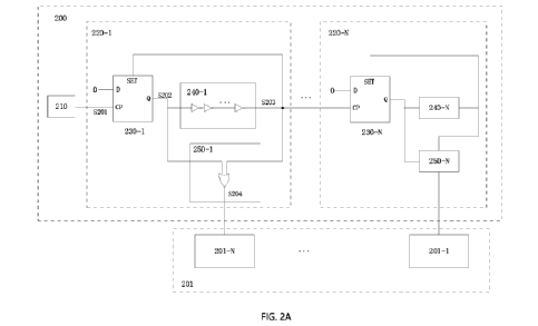
[ 0013] Fig. 1 shows a schematic diagram of a pipeline clock driving circuit
of the related art.
[0014] Fig. 2A shows a schematic diagram of a pipeline clock driving circuit
according to some
embodiments of the disclosure.
[0015] Fig. 2B shows a timing diagram of a pulse clock signal generated by a
pipeline clock driving
circuit according to some embodiments of the present disclosure.
[0016] Fig. 3A shows a schematic diagram of a pipeline clock driving circuit
according to other
embodiments of the disclosure.
[0017] Fig. 3B shows a timing diagram of a pulse clock signal generated by a
pipeline clock driving
circuit according to other embodiments of the disclosure.
[0018] Fig. 4 shows a schematic diagram of a pipeline clock driving circuit
according to further
embodiments of the disclosure.
[0019] Note that in the embodiments described below, one same reference
numeral is sometimes
shared between different drawings to denote a same portion or portions having
a same function, and a
repetitive description thereof will be omitted. In this specification, similar
reference numerals and letters are
used to designate similar items, and therefore, once a certain item is defined
in one drawing, further
5
CA 03165378 2022- 7- 19
discussion thereof is not required in subsequent drawings.
[0020] For ease of understanding, positions, sizes, ranges, and the like of
structures shown in the
drawings and the like do not necessarily indicate actual positions, sizes,
ranges, and the like. Therefore, the
disclosed invention is not limited to the positions, sizes, ranges, and the
like disclosed in the drawings and the
like. Furthermore, the drawings are not necessarily to scale, some features
may be enlarged to show details of
specific components.
6
CA 03165378 2022- 7- 19
DETAILED DESCRIPTION
[ 0021] Various exemplary embodiments of the present disclosure will now be
described in detail with
reference to the accompanying drawings. It should be noted that relative
arrangements of components and
steps, numerical expressions, and numerical values set forth in these
embodiments do not limit the scope of
the present disclosure unless specifically stated otherwise.
[0022] The following description of at least one exemplary embodiment is
merely illustrative in nature
and in no way serves as any limitation on this disclosure and its application
or use. That is, a hash engine
herein is shown illustratively to explain different embodiments of a circuit
in the present disclosure and is not
intended to be limiting. Those skilled in the art will appreciate that they
are merely illustrative of exemplary
ways in which the present disclosure can be implemented, rather than
exhaustive ways.
[0023] Techniques, methods, and devices known to one of ordinary skill in the
related art may not be
discussed in detail but should be regarded as part of the granted
specification where appropriate.
[0024] Fig. 1 shows a schematic diagram of a pipeline clock driving circuit
100 of the related art. The
pipeline clock driving circuit 100 is configured to provide a pulse clock
signal to a pipeline 101 comprising a
plurality of operation stages 101-1, ..., 101-(N-1), 101-N.
[0025] As shown in Fig. 1, the pipeline clock driving circuit 100 comprises a
clock source 110 and a
plurality of stages of clock driving circuits 120-1, 120-2, ..., 120-N. The
clock source 110 is coupled to an input
of a first stage of clock driving circuit 120-1 and is configured to provide a
basic clock signal. Each of the
plurality of stages of clock driving circuits 120-1, 120-2, ..., 120-N is
configured to provide the pulse clock
signal to one corresponding operation stage in the plurality of operation
stages 101-N, 101- (N-1), ..., 101-1
of the pipeline 101.
[0026] Each stage of clock driving circuit 120-1, 120-2, ..., 120-N comprises
a delay module 130-1,
130-2, ..., 130-N and a combinational logic module 140-1, 140-2, ..., 140-N
(e.g., NOR gate, NAND gate, etc.).
7
CA 03165378 2022- 7- 19
The delay module 130-1, 130-2, ..., 130-N is configured to delay an input
clock signal of that stage of clock
driving circuit 120-1, 120-2,..., 120-N. The combinational logic module 140-1,
140-2,..., 140-N is configured
to perform a logic operation (such as NOR, NAND, etc.) on the input clock
signal of that stage of clock driving
circuit 120-1, 120-2, ..., 120-N and the input clock signal delayed by the
delay module 130-1, 130-2,.,.,
130-N, and output the operation result thereof as the output pulse clock
signal of that stage of clock driving
circuit 120-1, 120-2, ..., 120-N, to be provided to one corresponding
operation stage 101-N, 101- (N-1), ...,
101-1 of the pipeline 101.
[ 0027] Typically, a duty cycle of the basic clock signal generated by the
clock source is 0.5. However, the
duty cycle will be increasingly poor in a process of the stage-by-stage
transfer of the clock signal through the
pipeline clock driving circuit. A main reason for the poor duty cycle of the
clock signal is accumulation of
manufacturing errors of combinational logic devices. In the process of the
stage-by-stage transfer of the clock
signal through the pipeline clock driving circuit, the clock signal will pass
through many combinational logic
devices such as buffers, inverters and the like. Due to a manufacturing
process, there are errors in
performance parameters of these combinational logic devices, and such errors
cause deviations in the clock
duty cycle. Moreover, with the stage-by-stage transfer of the clock signal,
influences caused by the parameter
errors of the combinational logic devices in the stages of clock driving
circuits accumulate continuously, and
therefore such deviations of the clock duty cycle gradually increase.
Therefore, the farther the clock driving
circuit is from the clock source, the poorer the duty cycle of the input clock
signal thereof, and
correspondingly, the poorer the pulse clock generated by it. In this way, the
requirements for the minimum
pulse width of the corresponding operation stage may not be met.
[0028] That is, deviations of duty cycles of the clock signals will occur due
to manufacturing errors of the
combinational logic devices (e.g., buffers, inverters, etc.) in the delay
modules 130-1, 130-2, ..., 130-N. In a
process of transferring the basic clock signal output from the clock source
110 through the stages of the clock
8
CA 03165378 2022- 7- 19
driving circuits 120-1, 120-2, ..., 120-N, such deviations of the duty cycle
will gradually accumulate, which
makes the clock pulse width of the operation stage (101-1) that is farther
from the clock source 110 poorer, so
that the requirement of that operation stage for the pulse width of the
working clock cannot be met.
[ 0029] To solve this problem, the present disclosure provides an improved
pipeline clock driving circuit,
in which a pulse width of a pulse clock signal generated by each stage of
clock driving circuit is independent
of its input clock signal.
[0030] Fig. 2A shows a schematic diagram of a pipeline clock driving circuit
200 according to some
embodiments of the present disclosure. Fig. 2B shows a timing diagram of a
pulse clock signal generated by a
pipeline clock driving circuit 200 according to some embodiments of the
present disclosure.
[0031] The pipeline clock driving circuit 200 is configured to provide a pulse
clock signal to a pipeline
201 comprising a plurality of operation stages 201-1, ..., 201-N.
[0032] As shown in Fig. 2A, the pipeline clock driving circuit 200 comprises a
clock source 210 and a
plurality of stages of clock driving circuits 220-1, ..., 220-N.
[ 0 033] The clock source 210 is coupled to an input of a first stage of clock
driving circuit 220-1 and is
configured to provide a basic clock signal. A duty cycle of the basic clock
signal provided by the clock source
210 can be 0.5, and a frequency thereof can be several hundred megahertz, e.g.
400-700MHz.
[0034] Inputs of other stages of clock driving circuits in the plurality of
stages of clock driving circuits
220-1, ..., 220-N than the first stage of clock driving circuit 220-1 are
coupled to output of previous stages of
clock driving circuits, wherein each stage of clock driving circuit 220-1,
..., 220-N is configured to provide the
pulse clock signal to one corresponding operation stage in the plurality of
operation stages 201-N, ..., 201-1
of the pipeline 201.
[ 0035] Each stage of clock driving circuit 220-1, ..., 220-N comprises a
trigger 230-1, ..., 230-N, a delay
module 240-1, ..., 240-N, and a combinational logic module 250-1, ..., 250-N.
9
CA 03165378 2022- 7- 19
[ 0 036] The trigger 230-1, ..., 230-N is coupled to an input of a present
stage of clock driving circuit. That
is, the trigger 230-1 in the first stage of clock driving circuit 220-1 is
coupled to an output of the clock source
210, and triggers in other stages of clock driving circuits are coupled to
outputs of previous stages of clock
driving circuits. The trigger 230-1, ..., 230-N can be an edge trigger. A type
and connection mode of the
trigger 230-1, ..., 230-N can be configured as needed.
[ 0 037] In Fig. 2A, an embodiment of the trigger 230-1, ..., 230-N as a
rising edge D trigger is shown. In
the embodiment shown in Fig. 2A, a SET end of the trigger 230-1, ..., 230-N is
coupled to an output of the
delay module 240-1, ..., 240-N, a D end is fixed to a low level (i.e., logic
'0"), a CP end is coupled to an output
of a previous stage of clock driving circuit, and an output end Q is coupled
to the delay module 240-1.....
240-N as an input thereof. Under the condition that the SET end signal of the
rising edge D trigger is a high
level, the output end Q is always the high level. When the SET end signal is a
low level, the output end Q
becomes a signal value of the D end every time a rising edge of the CP end
signal arrives. In other
embodiments, the trigger 230-1, ..., 230-N can be, for example, a falling edge
trigger, and its connection
mode can be adjusted accordingly (which will be described in detail below in
an embodiment shown in Fig.
3A).
[ 0038] The input of the delay module 240-1, ..., 240-N is coupled to the
output of the trigger 230-1, ...,
230-N. The delay module 240-1, ..., 240-N is configured to delay the pulse
signal output by the trigger 230-1,
..., 230-N, feed the delayed pulse signal back to the trigger 230-1, ..., 230-
N and output the delayed pulse
signal to a next stage of clock driving circuit. In a preferred embodiment,
the delay module 240-1, ..., 240-N
also inverts the pulse signal output by the trigger 230-1, ..., 230-N. The
delay module 240-1, ..., 240-N can be
implemented by several buffers and/or inverters. In a preferred embodiment,
the delay module 240-1.....
240-N can be composed of an odd number of inverters, as shown in Fig. 2A. In
other embodiments, the delay
module 240-1, ..., 240-N can be composed of several buffers and an odd number
of inverters.
CA 03165378 2022- 7- 19
[0039] The combinational logic module 250-1, ..., 250-N is coupled to outputs
of the trigger 230-1, ...,
230-N and the delay module 240-1,..., 240-N. The combinational logic module
250-1,..., 250-N performs a
combinational logic operation on the pulse signal output by the trigger 230-1,
..., 230-N and the delayed
pulse signal output by the delay module 240-1, ..., 240-N to generate the
pulse clock signal to be provided to
one corresponding operation stage 201-N, ..., 201-1 of the pipeline 201. The
combinational logic module
250-1, ..., 250-N can be designed according to the type of the trigger 230-1,
..., 230-N. In the embodiment
shown in Fig. 2A, under the condition that the trigger 230-1, ..., 230-N is a
rising edge D trigger, the
combinational logic module 250-1, ..., 250-N can be composed of OR gates or
NOR gates. In other
embodiments, the combinational logic module 250-1, ..., 250-N can be composed
of AND gates or NAND
gates (which will be described in detail below in the embodiment shown in Fig.
3A).
[0040] In a preferred embodiment, as shown in Fig. 2A, a direction in which
the pulse signal is
transferred in the plurality of stages of clock driving circuits 220-1, ...,
220-N is opposite to a direction in
which a data signal is transferred in the plurality of operation stages 201-1,
..., 201-N of the pipeline. That is,
the first stage of clock driving circuit 220-1 is configured to provide the
pulse clock signal to the last operation
stage 201-N, and the last stage of clock driving circuit 220-N is configured
to provide the pulse clock signal to
the first operation stage 201-1, and so on. Such an arrangement can more
easily meet the requirements of
operation timing of the operation stages 201-1, ..., 201-N.
[ 0 0 41] Referring to Fig. 2B, taking the first stage of clock driving
circuit 220-1 as an example, timing of
generating the pulse clock signal thereof will be described below.
[ 0042] The CP end of the trigger 230-1 receives the basic clock signal S201
as an input signal from the
clock source 210 (accordingly, CP ends of next stages of triggers receive
output signals S203 as input signals
from the outputs of the delay modules in previous stages of clock driving
circuits, respectively), and provides
a pulse signal S202 at the output end Q to the delay module 240-1 and one
input end of the combinational
11
CA 03165378 2022- 7- 19
logic module 250-1 (which is a NOR gate in this embodiment). The delay module
240-1 inverts and delays the
pulse signal S202 to obtain an output signal S203, and provides the output
signal S203 to the SET end of the
trigger 230-1 and the other input end of the combinational logic module 250-1,
respectively, and provides the
output signal S203 as an input signal of a next stage of clock driving
circuit.
[ 0043] After the entire system is powered on, when the clock source 210 has
not output the basic clock
signal S201, the pulse signal S202 at the output end Q of the trigger 230-1
will stabilize at the high level.
Accordingly, the output signal S203 of the delay module 240-1 stabilizes at
the low level, i.e., the SET end of
the trigger 230-1 is the low level, and the input signal of the next stage of
clock driving circuit is also the low
level (corresponding to the input signal S201 of the first stage of clock
driving circuit 220-1). Therefore, the
input signals of the combinational logic module 250-1 (NOR gate) are the high
level (S202) and the low level
(S203),respectively, and the output pulse clock signal S204 thereof is the low
level.
[0044] At time t1, the clock source 210 starts outputting the basic clock
signal S201. The basic clock
signal S201 has a period of T.
[ 0045] As shown in Fig. 2B, when the signal S201 changes from the low level
to the high level, the signal
rising edge of the CP end of the trigger 230-1 arrives, and the SET end signal
(S203) is still the low level, so
that the signal S202 of the output end Q of the trigger 230-1 becomes the
signal value of the D end, i.e., the
low level. Accordingly, the input signals of the combinational logic module
250-1 (NOR gate) are the low level
(S202) and the low level (S203), respectively, and the output pulse clock
signal S204 thereof becomes the high
level.
[ 0 046] After to, at time t2, the output signal S203 of the delay module 240-
1 becomes the high level, to is
a delay time between the signals S203 and S202, which is determined by
configuration of the delay module
240-1. In the embodiment shown in Fig. 2A, to is a sum of delay times of the
plurality of inverters in the delay
module 240-1.
12
CA 03165378 2022- 7- 19
[0047] Accordingly, as shown in Fig. 2B, on the one hand, the SET end of the
trigger 230-1 becomes the
high level, so that the signal S202 at the output end Q of the trigger 230-1
becomes the high level. On the
other hand, the input signals of the combinational logic module 250-1 (NOR
gate) are the high level (S202)
and the high level (S203), respectively, and the output pulse clock signal
S204 thereof becomes the low level.
[0048] After to again, at time t3, the output signal S203 of the delay module
240-1 becomes the low
level.
[ 0049] Accordingly, as shown in Fig. 2B, on the one hand, the SET end of the
trigger 230-1 becomes the
low level, but a signal rising edge has not arrived at the CP end, so that the
signal S202 of the output end Q of
the trigger 230-1 still remains the high level. On the other hand, the input
signals of the combinational logic
module 250-1 (NOR gate) are the high level (S202) and the low level (S203),
respectively, and the output pulse
clock signal S204 thereof is still the low level.
[0050] Thereafter, the values of the signals S202, S203, S204 remain
unchanged. Until time t4, a next
period of the basic clock signal S201 starts. One period T of the basic clock
signal S201 passes from the time
t1 to the time t4.
[ 0 051] At time t4, the signal S201 becomes the high level.
[ 0052] As shown in Fig. 2B, when the signal S201 changes from the low level
to the high level, the signal
rising edge arrives at the CP end of the trigger 230-1, and the SET end signal
(S203) is still the low level, so
that the signal S202 of the output end Q of the trigger 230-1 becomes the low
level. Accordingly, the pulse
clock signal S204 at the output end of the combinational logic module 250-1
(NOR gate) becomes the high
level.
[ 0053] After to, at time t5, the output signal S203 of the delay module 240-1
becomes the high level.
[ 0054] Accordingly, as shown in Fig. 2B, on the one hand, the SET end of the
trigger 230-1 becomes the
13
CA 03165378 2022- 7- 19
high level, so that the signal S202 of the output end Q of the trigger 230-1
becomes the high level. On the
other hand, the pulse clock signal S204 at the output end of the combinational
logic module 250-1 becomes
the low level.
[0055] After to again, at time t6, the output signal S203 of the delay module
240-1 becomes the low
level.
[0056] Accordingly, as shown in Fig. 2B, the signal S202 of the output end Q
of the trigger 230-1 still
remains the high level, and the pulse clock signal S204 at the output end of
the combinational logic module
250-1 is still the low level.
[ 0057] In this way, the pulse clock signal S204 with a period of T and a
pulse width of to is generated at
the output end of the combinational logic module 250-1. The pulse clock signal
S204 is provided to the
corresponding operation stage 201-N as the working clock.
[0058] In addition, the output signal S203 is generated at the output end of
the delay module 240-1,
and the output signal S203 is simultaneously used as the input signal of the
next stage of clock driving circuit
(equivalent to the input signal S201 of the first stage of clock driving
circuit 220-1). The rising edge of the
output signal S203 is used for triggering the trigger of the next stage of
clock driving circuit. As shown in Fig.
2B, the rising edge of the output signal S203 is delayed to as compared to the
rising edge of the input signal
S201. Similarly, the rising edge of the output signal generated by each stage
of clock driving circuit is delayed
to as compared to the rising edge of the input signal of that stage of clock
driving circuit, which meets the
working requirements of the operation stages of the pipeline.
[0059] In this way, the pulse clock signal generated by each stage of clock
driving circuit has a pulse
width of to, which is decided only by the configuration of that stage of clock
driving circuit and is independent
of the input signal of that stage of clock driving circuit. Although
manufacturing errors of the combinational
logic devices in each stage of clock driving circuits may still cause the
deviations in the pulse widths of the
14
CA 03165378 2022- 7- 19
stages of input signals and output signals, the pulse width of the pulse clock
signal generated by each stage
of clock driving circuit is independent of the pulse width of the input signal
thereof. Thus, such deviations of
the pulse widths will not accumulate continuously as the signals are
transferred in the stages of clock driving
circuits. That is, the possible deviation of the pulse width of the pulse
clock signal generated by each stage of
clock driving circuit is independent of possible manufacturing errors of
combinational logic devices in
previous stages of clock driving circuits, and is only related to the possible
manufacturing errors of the
combinational logic devices in that stage of clock driving circuit. Such a
manufacturing error is typically small,
so that the resultant pulse width deviation is acceptable.
[0060] Fig. 3A shows a schematic diagram of a pipeline clock driving circuit
300 according to other
embodiments of the present disclosure. Fig. 3B shows a timing diagram of a
pulse clock signal generated by a
pipeline clock driving circuit 300 according to other embodiments of the
present disclosure.
[ 0 0 61] The pipeline clock driving circuit 300 is configured to provide a
pulse clock signal to a pipeline
301 that comprises a plurality of operation stages 301-1,..., 301-N. As shown
in Fig. 3A, the pipeline clock
driving circuit 300 comprises a clock source 310 and a plurality of stages of
clock driving circuits 320-1,...,
320-N.
[ 0 0 62] The clock source 310 is coupled to an input of a first stage of
clock driving circuit 320-1 and is
configured to provide a basic clock signal. Inputs of other stages of clock
driving circuits in the plurality of
stages of clock driving circuits 320-1, ..., 320-N than the first stage of
clock driving circuit 320-1 are coupled
to outputs of previous stages of clock driving circuits, wherein each stage of
clock driving circuit 320-1, ...,
320-N is configured to provide the pulse clock signal to one corresponding
operation stage in the plurality of
operation stages 320-1, ..., 320-N of the pipeline 301.
[ 0063] Each stage of clock driving circuit 320-1, ..., 320-N comprises a
trigger 330-1, ..., 330-N, a delay
module 340-1, ..., 340-N, and a combinational logic module 350-1, ..., 350-N.
CA 03165378 2022- 7- 19
[0064] The trigger 330-1, ..., 330-N is coupled to an input of a present stage
of clock driving circuit. That
is, the trigger 330-1 in the first stage of clock driving circuit 320-1 is
coupled to an output of the clock source
310, and triggers in other stages of clock driving circuits are coupled to
outputs of previous stages of clock
driving circuits.
[0065] In Fig. 3A, an embodiment in which the trigger 330-1, ..., 330-N is a
falling edge D trigger is
shown. In the embodiment shown in Fig. 3A, a RESET end of the trigger 330-1,
..., 330-N is coupled to an
output of the delay module 340-1, ..., 340-N, a D end is fixed to a high level
(i.e., logic "1"), a CPN end is
coupled to an output of a previous stage of clock driving circuit, and an
output end Q is coupled to the delay
module 340-1, ..., 340-N as an input thereof. Under the condition that the
RESET end signal of the falling
edge D trigger is a low level, the output end Q is always the low level. Under
the condition that the RESET end
signal is the high level, the output end Q becomes a signal value of the D end
every time a falling edge of the
CPN end signal arrives.
[ 0066] The input of the delay module 340-1, ..., 340-N is coupled to the
output of the trigger 330-1,...,
330-N. The delay module 340-1, ..., 340-N is configured to delay the pulse
signal output by the trigger 330-1,
..., 330-N, feed the delayed pulse signal back to the trigger 330-1, ..., 330-
N, and output the delayed pulse
signal to a next stage of clock driving circuit. In a preferred embodiment,
the delay module 340-1, ..., 340-N
also inverts the pulse signal output by the trigger 330-1, ..., 330-N. In the
embodiment shown in Fig. 3A, the
delay module 340-1, ..., 340-N can be composed of an odd number of inverters.
[ 0 0 67] The combinational logic module 350-1, ..., 350-N is coupled to
outputs of the trigger 330-1, ...,
330-N and the delay module 340-1, ..., 340-N. The combinational logic module
350-1, ..., 350-N performs a
combinational logic operation on the pulse signal output by the trigger 330-1,
..., 330-N and the delayed
pulse signal output by the delay module 340-1, ..., 340-N to generate the
pulse clock signal to be provided to
one corresponding operation stage 301-N, ..., 301-1 of the pipeline 301. In
the embodiment shown in Fig. 3A,
16
CA 03165378 2022- 7- 19
under the condition that the trigger 330-1, ..., 330-N is the falling edge D
trigger, the combinational logic
module 350-1,..., 350-N can be composed of a NAND gate.
[ 0 0 68] Referring to Fig. 3B, taking the first stage of clock driving
circuit 320-1 as an example, timing of
generating the pulse clock signal thereof will be described below.
[ 0069] The CPN end of the trigger 330-1 receives the basic clock signal S301
as an input signal from the
clock source 310 (accordingly, CPN ends of next stages of triggers receive
output signals S303 as input signals
from the outputs of the delay modules in previous stages of the clock driving
circuits, respectively), and
provides a pulse signal S302 at the output end Q to the delay module 340-1 and
one input end of the
combinational logic module 350-1 (which is a NAND gate in this embodiment).
The delay module 340-1
inverts and delays the pulse signal S302 to obtain an output signal S303, and
provides the output signal S303
to the RESET end of the trigger 330-1 and the other input end of the
combinational logic module 350-1,
respectively, and provides the output signal S303 as an input signal of a next
stage of clock driving circuit.
[ 0070] After the entire system is powered on, when the clock source 310 has
not output the basic clock
signal S301, the pulse signal S302 at the output end Q of the trigger 330-1
will stabilize at the low level.
Accordingly, the output signal S303 of the delay module 340-1 stabilizes at
the high level, i.e., the RESET end
of the trigger 330-1 is the high level, and the input signal of the next stage
of clock driving circuit is also the
high level (corresponding to the input signal S301 of the first stage of clock
driving circuit 320-1). Therefore,
the input signals of the combinational logic module 350-1 (NAND gate) are the
low level (S302) and the high
level (S303), respectively, and the output pulse clock signal S304 thereof is
the high level.
[0071] At time t1, the clock source 310 starts outputting the basic clock
signal S301. The basic clock
signal S301 has a period of T.
[ 0 072] As shown in Fig. 3B, when the signal S301 changes from the high level
to the low level, a signal
falling edge arrives at the CPN end of the trigger 330-1, and the RESET end
signal (S303) is still the high level,
17
CA 03165378 2022- 7- 19
so that the signal S302 of the output end Q of the trigger 330-1 becomes the
signal value of the D end, i.e.,
the high level. Accordingly, the input signals of the combinational logic
module 350-1 (NAND gate) are the
high level (S302) and the high level (S303),respectively, and the output pulse
clock signal S304 thereof
becomes the low level.
[ 0073] After to, at time t2, the output signal S303 of the delay module 340-1
becomes the low level, to is
a delay time between the signals S303 and S302, which is decided by the
configuration of the delay module
340-1. In the embodiment shown in Fig. 3A, to is a sum of delay times of a
plurality of inverters in the delay
module 340-1.
[ 0074] Accordingly, as shown in Fig. 3B, on the one hand, the RESET end of
the trigger 330-1 becomes
the low level, so that the signal S302 at the output end Q of the trigger 330-
1 becomes the low level. On the
other hand, the input signals of the combinational logic module 350-1 (NAND
gate) are the low level (S302)
and the low level (S303), respectively, and the output pulse clock signal S304
thereof becomes the high level.
[0075] After to again, at time t3, the output signal S303 of the delay module
340-1 becomes the high
level.
[ 0076] Accordingly, as shown in Fig. 3B, on the one hand, the RESET end of
the trigger 330-1 becomes
the high level, but the signal rising edge has not arrived at the CPN end, so
that the signal S302 at the output
end Q of the trigger 330-1 still remains the low level. On the other hand, the
input signals of the
combinational logic module 350-1 (NAND gate) are the low level (S302) and the
high level (S303),
respectively, and the output pulse clock signal S304 thereof is still the high
level.
[0077] Thereafter, the values of the signals S302, S303, S304 remain
unchanged. Until time t4, a next
period of the basic clock signal S301 starts. One period T of the basic clock
signal S301 passes from the time
t1 to the time t4.
[ 0078] At time t4, the signal S301 becomes the low level.
18
CA 03165378 2022- 7- 19
[0079] As shown in Fig. 3B, when the signal S301 changes from the high level
to the low level, the signal
falling edge arrives at the CPN end of the trigger 330-1, so that the signal
S302 of the output end Q of the
trigger 330-1 becomes the high level. Accordingly, the pulse clock signal S304
at the output end of the
combinational logic module 350-1 (NAND gate) becomes the low level.
[ 0080] After to, at time t5, the output signal S303 of the delay module 340-1
becomes the low level.
[ 0081] Accordingly, as shown in Fig. 3B, on the one hand, the RESET end of
the trigger 330-1 becomes
the low level, so that the signal S302 of the output end Q of the trigger 330-
1 becomes the low level. On the
other hand, the pulse clock signal S304 at the output end of the combinational
logic module 350-1 becomes
the high level.
[0082] After to again, at time t6, the output signal S303 of the delay module
340-1 becomes the high
level.
[0083] Accordingly, as shown in Fig. 3B, the signal S302 at the output end Q
of the trigger 330-1 still
remains the low level, and the pulse clock signal S304 at the output end of
the combinational logic module
350-1 is still high level.
[ 0084] In this way, the pulse clock signal S304 with a period of T and a
pulse width of to is generated at
the output end of the combinational logic module 350-1. The pulse clock signal
S304 is provided to the
corresponding operation stage 301-N as a working clock.
[0085] In addition, the output signal S303 is generated at the output end of
the delay module 340-1,
and the output signal S303 is simultaneously used as the input signal of the
next stage of clock driving circuit
(equivalent to the input signal S301 of the first stage of clock driving
circuit 320-1). The falling edge of the
output signal S303 is used for triggering a trigger of the next stage of clock
driving circuit. As shown in Fig. 3B,
the falling edge of the output signal S303 is delayed to as compared to the
falling edge of the input signal
S301. Similarly, the falling edge of the output signal generated by each stage
of clock driving circuit is delayed
19
CA 03165378 2022- 7- 19
to as compared to the falling edge of the input signal of that stage of clock
driving circuit, which meets the
working requirements of the operation stages of the pipeline.
[0086] As described above, the pulse width of the pulse clock generated by the
pipeline clock driving
circuit according to the present disclosure is decided by the time to delayed
by the delay module. In a
preferred embodiment, the delay module is composed of inverters. The greater
the number of inverters is, the
greater the pulse width of the generated pulse clock signal will be, and the
lower the working frequency of the
pipeline will be. In engineering practices, it is generally expected to make
the working frequency of the
pipeline as high as possible under the condition that the pulse width of the
pulse clock can meet the
requirements. To this end, the present disclosure provides a further improved
pipeline clock driving circuit, in
which the number of inverters constituting the delay module can be flexibly
adjusted.
[0087] Fig. 4 shows a schematic diagram of a pipeline clock driving circuit
400 according to further
embodiments of the present disclosure.
[ 0088] The pipeline clock driving circuit 400 is configured to provide a
pulse clock signal for a pipeline.
As shown in Fig. 4, the pipeline clock driving circuit 400 comprises a clock
source 410 and a plurality of stages
of clock driving circuits.
[ 0089] Taking a first stage of clock driving circuit 420-1 as an example, it
is configured to provide a pulse
clock signal for the last operation stage 401-N of the pipeline. The first
stage of clock driving circuit 420-1
comprises a trigger 430-1, a delay module 440-1, and a combinational logic
module 450-1. Configurations of
the trigger 430-1, the delay module 440-1 and the combinational logic module
450-1 are similar to those of
the embodiment shown in Fig. 2A, and the timing of the generated pulse clock
signal thereof is similar to that
shown in Fig. 2B, which are not repeated here.
[0090] Unlike the embodiment shown in Fig. 2A, the delay module 440-1 is
composed of a plurality of
inverters and one or more data selectors. The data selector is configured such
that the plurality of inverters
CA 03165378 2022- 7- 19
form a plurality of signal paths, and the number of inverters in each signal
path is odd. In the embodiment
shown in Fig. 4, the delay module 440-1 is composed of seven inverters and
three data selectors, which form
four signal paths including one, three, five, and seven inverters,
respectively. Therefore, in the embodiment
shown in Fig. 4, by switching states of the three data selectors, the
generated clock pulse signal can be made
to have four different pulse widths (i.e., corresponding to a sum of the delay
times of one, three, five, and
seven inverters, respectively).
[ 0 0 91] Therefore, the state of the data selector can be flexibly and
conveniently changed according to
the actual pulse width requirements, to make the working frequency of the
pipeline as high as possible, so
that working efficiency of the chip is improved.
[ 0092] The configuration of the delay module 440-1 shown in Fig. 4 is taken
as an example only. In other
embodiments, the delay module 440-1 can be composed of any suitable number of
inverters and data
selectors in any suitable configuration to form a plurality of signal paths,
such that a suitable number of
inverters are included in each signal path. In a preferred embodiment, the
number of inverters in each signal
path is different.
[ 0 093] The operation circuit according to the present disclosure can be
implemented in various suitable
manners such as software, hardware, a combination of software and hardware,
and the like. In one
implementation, a computing chip can comprise one or more of the pipeline
clock driving circuits described
above. In one implementation, a hashboard can comprise one or more computing
chips. In one
implementation, a computing device can comprise one or more hashboards. A
plurality of hashboards can
perform computing tasks in parallel.
[0094] In all examples shown and discussed herein, any specific value should
be construed as exemplary
only and not as a limitation. Therefore, other examples of the exemplary
embodiment can have different
values.
21
CA 03165378 2022- 7- 19
[0095] It should be further understood that terms "include/comprise", when
used herein, specify the
presence of stated features, entirety, steps, operations, units, and/or
components, but do not preclude the
presence or addition of one or more other features, entirety, steps,
operations, units and/or components,
and/or combinations thereof.
[ 0096] While some specific embodiments of the present disclosure have been
shown in detail by way of
examples, it should be understood by those skilled in the art that the
foregoing examples are intended to be
illustrative only and do not limit the scope of the present disclosure. It
should be appreciated by those skilled
in the art that the above embodiments can be modified without departing from
the scope and spirit of the
present disclosure. The scope of the disclosure is defined by the attached
claims.
22
CA 03165378 2022- 7- 19